US6275117B1 - Circuit and method for controlling an output of a ring oscillator - Google Patents
Circuit and method for controlling an output of a ring oscillatorDownload PDFInfo
- Publication number
- US6275117B1 US6275117B1US09/216,460US21646098AUS6275117B1US 6275117 B1US6275117 B1US 6275117B1US 21646098 AUS21646098 AUS 21646098AUS 6275117 B1US6275117 B1US 6275117B1
- Authority
- US
- United States
- Prior art keywords
- transistor
- bias
- signal
- variable impedance
- output signal
- Prior art date
- Legal status (The legal status is an assumption and is not a legal conclusion. Google has not performed a legal analysis and makes no representation as to the accuracy of the status listed.)
- Expired - Lifetime
Links
- 238000000034methodMethods0.000titleclaimsabstractdescription14
- 230000010355oscillationEffects0.000claimsdescription11
- 229920006395saturated elastomerPolymers0.000claimsdescription6
- 238000010586diagramMethods0.000description8
- 230000002411adverseEffects0.000description1
- 230000007423decreaseEffects0.000description1
Images


Classifications
- H—ELECTRICITY
- H03—ELECTRONIC CIRCUITRY
- H03K—PULSE TECHNIQUE
- H03K3/00—Circuits for generating electric pulses; Monostable, bistable or multistable circuits
- H03K3/02—Generators characterised by the type of circuit or by the means used for producing pulses
- H03K3/027—Generators characterised by the type of circuit or by the means used for producing pulses by the use of logic circuits, with internal or external positive feedback
- H03K3/03—Astable circuits
- H03K3/0315—Ring oscillators
- H—ELECTRICITY
- H03—ELECTRONIC CIRCUITRY
- H03L—AUTOMATIC CONTROL, STARTING, SYNCHRONISATION OR STABILISATION OF GENERATORS OF ELECTRONIC OSCILLATIONS OR PULSES
- H03L7/00—Automatic control of frequency or phase; Synchronisation
- H03L7/06—Automatic control of frequency or phase; Synchronisation using a reference signal applied to a frequency- or phase-locked loop
- H03L7/08—Details of the phase-locked loop
- H03L7/085—Details of the phase-locked loop concerning mainly the frequency- or phase-detection arrangement including the filtering or amplification of its output signal
- H03L7/089—Details of the phase-locked loop concerning mainly the frequency- or phase-detection arrangement including the filtering or amplification of its output signal the phase or frequency detector generating up-down pulses
- H03L7/0891—Details of the phase-locked loop concerning mainly the frequency- or phase-detection arrangement including the filtering or amplification of its output signal the phase or frequency detector generating up-down pulses the up-down pulses controlling source and sink current generators, e.g. a charge pump
- H—ELECTRICITY
- H03—ELECTRONIC CIRCUITRY
- H03L—AUTOMATIC CONTROL, STARTING, SYNCHRONISATION OR STABILISATION OF GENERATORS OF ELECTRONIC OSCILLATIONS OR PULSES
- H03L7/00—Automatic control of frequency or phase; Synchronisation
- H03L7/06—Automatic control of frequency or phase; Synchronisation using a reference signal applied to a frequency- or phase-locked loop
- H03L7/08—Details of the phase-locked loop
- H03L7/099—Details of the phase-locked loop concerning mainly the controlled oscillator of the loop
- H03L7/0995—Details of the phase-locked loop concerning mainly the controlled oscillator of the loop the oscillator comprising a ring oscillator
Definitions
- the present inventionrelates to voltage controlled oscillators (VCOs) generally and, more particularly, to a circuit and method for improving the analog swing of a ring oscillator.
- VCOsvoltage controlled oscillators
- a VCOIn a VCO, there is a ring oscillator that generates two differential analog signals that are presented to a comparator.
- the comparatorconverts the differential analog signals to CMOS levels.
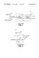
- FIG. 1a diagram of a circuit 10 is shown illustrating such a conventional VCO.
- the circuit 10comprises a pump-up circuit 12 , a pump-down circuit 14 and a VCO circuit 16 .
- the VCO circuit 16comprises a ring oscillator 18 and an analog-to-digital CMOS converter circuit 20 .
- the signals A and Abare converted to clock signals CLK and CLKb by the circuit 20 .
- the ring oscillator stage 18comprises a transistor 21 , a transistor 22 , a transistor 24 , a voltage controlled resistor (VCR) 26 and a VCR 28 .
- the delay in the ring oscillator stage 18is proportional to the capacitance and the impedance on nodes B and Bb.
- the ring oscillator 18can have a number of stages (e.g., the number of stages can be N, 2N, 2N+1, etc.).
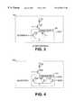
- the leg 29comprises a current source 30 , a transistor 32 , and a VCR 26 (or 28 ).
- the VCRcomprises a transistor 34 and a transistor 36 .
- a control voltagei.e., Vcontrol
- the transistor 34may be in a saturation mode.
- the impedance at the drain node Dwill be very high, which can hinder proper and stable oscillation of the oscillator.
- the voltage controlled resistor 26controls the delay in each ring oscillator stage which, in turn, determines the frequency of oscillation of the output signal OUT.
- FIG. 3illustrates a conventional approach where the VCR 26 consists of two transistors (i.e., transistor 34 and 36 ). As the control voltage Vcontrol increases, the impedance of the transistor 34 decreases, which reduces the delay in the particular stage and increases the frequency of oscillation of the VCO. The transistor 36 helps the oscillation at low control voltages when the transistor 34 is cut-off or at high control voltages when the transistor 34 is in saturation.
- the drain node DWhen the transistor 34 is in saturation and the transistor 36 is cut-off, the drain node D will see a high impedance. This may adversely affect oscillation and reduce the oscillation swing of the ring oscillator 18 . Also, when the transistor 34 is cut-off, the node D will not properly oscillate, because it needs to be greater than the threshold voltage (i.e., VTNMOS) to turn on the transistor 36 .
- the threshold voltagei.e., VTNMOS
- the present inventionconcerns a circuit and method configured to generate a variable impedance.
- the circuitmay comprise a voltage controlled resistor configured to generate the variable impedance in response to (i) a first transistor configured to receive a first control signal and (ii) a bias transistor configured to receive a bias signal.
- the variable impedancemay be generated in further response to a clamp transistor.
- the objects, features and advantages of the present inventioninclude providing a circuit a method for controlling an output of a ring oscillator stage that (i) improves the analog swing on the VCO, (ii) provides stable oscillation and (iii) reduces VCO gain variation.
- FIG. 1is a block diagram of a conventional VCO
- FIG. 2is a diagram of a conventional ring oscillator stage that may be used with the circuit of FIG. 1;
- FIG. 3is a circuit diagram of a conventional leg of a ring oscillator stage
- FIG. 4is a circuit diagram of a ring oscillator stage in accordance with a preferred embodiment of the present invention.
- FIG. 5is a general plot illustrating the drain voltage versus the drain current of the voltage controlled resistor of FIG. 4 compared to the voltage controlled resistor of FIG. 2;
- FIG. 6is a more detailed plot of the voltage response of the circuit of FIG. 4 as compared to the circuit of FIG. 2;
- FIG. 7is a plot of a resistor versus a no resistor comparison.
- FIG. 8is a plot of the analog swing versus voltage.
- the circuit 100generally comprises a VCR 101 , a current source 102 and a transistor 104 .
- the VCR 101generally comprises a transistor 106 , a transistor 108 and a transistor 110 .
- the gate of the transistor 110generally receives a control signal (e.g., BIAS).
- BIASmay cause the transistor 110 to generally remain in a linear region.
- the transistor 110may help to improve the overall impedance of the VCR when the transistor 106 is saturated and the transistor 108 is cut-off. Also, when the transistor 106 is cut-off, the transistor 110 will generally provide a low enough impedance for the drain node D to provide proper oscillation of the ring oscillator when the transistor 108 is cut-off. While the transistors 106 , 108 and 110 are shown implemented using NMOS transistors, PMOS transistors may be substituted to meet the design criteria of a particular implementation.
- the transistor 110is generally a weak transistor compared to the transistors 106 and 108 .
- the transistors 106is sized as 8/2 and the transistor 108 is sized as 8/2 or 6/2 (i.e., having a channel width of 8 (or 6) ⁇ m (i.e., 10 ⁇ 6 m) and a channel length of 2 ⁇ m)
- the transistor 110may have, in one example, a channel width of 2 ⁇ m and a channel length of 20 ⁇ m.
- the transistor 110may be 1% to 30% as strong as the transistor 106 and the transistor 108 may be 10%-150% as strong as the transistor 106 .
- the bias provided by the transistor 110may be such as it compensates for temperature and process variations.
- One example of a circuit that may generate the signal BIASmay be found in co-pending application U.S. Ser. No. 08/824,369, which is hereby incorporated by reference in its entirety.
- other circuits that generate bias signals that compensate for temperature and process variationsmay also be used.
- the transistor 108may be a clamp transistor that may control the voltage swing of the output of the ring oscillator (e.g., the ring oscillator 18 ).
- the transistor 108may control, or limit, the high end of the voltage of the ring oscillator.
- FIG. 5a plot of the drain voltage versus the drain current of the voltage controlled resistor of FIG. 4 (i.e., 26 ) compared to the voltage controlled resistor of FIG. 3 (i.e., 101 ) is shown.
- the plot circuit 101is labeled as “NEW” and the plot of the circuit 26 is labeled as “OLD”.
- FIG. 6a more detailed plot illustrating a DC sweep of the node D for the circuit 101 versus the circuit 26 is shown.
- the signal Vcontrolis presented at 0.8 volts to generate the signal NEW and the signal OLD.
- the signal Vcontrolis generated at 1.2 volts to generate the plot of the signal NEW′ and the signal OLD′.
- the signal Vcontrolis generated as 1.6 volts to generate the signal NEW′′ and the signal OLD′′.
- Each of the plotsi.e., NEW, NEW′ and NEW′′
- a plot of the frequency versus voltage of the circuit 18is shown implemented with the old VCRs (i.e., 26 ) and new VCRs (i.e., 101 ).
- the plot using the new VCR(s) 101is shown as the plot NEW and the plot using the old VCR(s) 26 is shown as the plot OLD.
- the plot NEWdoes not exhibit the “dip” 200 as shown by the plot OLD.
- FIG. 8a diagram illustrating the swing of the circuit 18 implemented with the old VCRs (i.e., 26 ) and new VCRs (i.e., 101 ).
- the plot using the new VCR(s) 101is shown as the plot NEW and the plot of the old VCR(s) 26 is shown as the plot OLD. While the plot NEW exhibits a slight “bump” 202 , the bump 202 is not as drastic as the bump in the plot OLD. Additionally, the plot NEW shows an improved swing compared to the plot OLD.
Landscapes
- Inductance-Capacitance Distribution Constants And Capacitance-Resistance Oscillators (AREA)
Abstract
Description
Claims (20)
Priority Applications (1)
| Application Number | Priority Date | Filing Date | Title |
|---|---|---|---|
| US09/216,460US6275117B1 (en) | 1998-12-18 | 1998-12-18 | Circuit and method for controlling an output of a ring oscillator |
Applications Claiming Priority (1)
| Application Number | Priority Date | Filing Date | Title |
|---|---|---|---|
| US09/216,460US6275117B1 (en) | 1998-12-18 | 1998-12-18 | Circuit and method for controlling an output of a ring oscillator |
Publications (1)
| Publication Number | Publication Date |
|---|---|
| US6275117B1true US6275117B1 (en) | 2001-08-14 |
Family
ID=22807158
Family Applications (1)
| Application Number | Title | Priority Date | Filing Date |
|---|---|---|---|
| US09/216,460Expired - LifetimeUS6275117B1 (en) | 1998-12-18 | 1998-12-18 | Circuit and method for controlling an output of a ring oscillator |
Country Status (1)
| Country | Link |
|---|---|
| US (1) | US6275117B1 (en) |
Cited By (43)
| Publication number | Priority date | Publication date | Assignee | Title |
|---|---|---|---|---|
| US6911871B1 (en)* | 2003-03-11 | 2005-06-28 | Applied Micro Circuits Corporation | Circuit with voltage clamping for bias transistor to allow power supply over-voltage |
| US20060267701A1 (en)* | 2005-05-27 | 2006-11-30 | Robert Eilers | Method and system for dynamically calculating values for tuning of voltage-controlled crystal oscillators |
| US7173501B1 (en) | 2003-06-27 | 2007-02-06 | Cypress Semiconductor Corporation | Dual slope temperature dependent oscillator |
| US7187245B1 (en) | 2003-09-25 | 2007-03-06 | Cypress Semiconductor Corporation | Amplitude control for crystal oscillator |
| US7332976B1 (en) | 2005-02-04 | 2008-02-19 | Cypress Semiconductor Corporation | Poly-phase frequency synthesis oscillator |
| US7400183B1 (en) | 2005-05-05 | 2008-07-15 | Cypress Semiconductor Corporation | Voltage controlled oscillator delay cell and method |
| US20100085127A1 (en)* | 2008-10-03 | 2010-04-08 | Kanan Saurabh | Circuit for voltage controlled oscillator |
| US7737724B2 (en) | 2007-04-17 | 2010-06-15 | Cypress Semiconductor Corporation | Universal digital block interconnection and channel routing |
| US7761845B1 (en) | 2002-09-09 | 2010-07-20 | Cypress Semiconductor Corporation | Method for parameterizing a user module |
| US7765095B1 (en) | 2000-10-26 | 2010-07-27 | Cypress Semiconductor Corporation | Conditional branching in an in-circuit emulation system |
| US7770113B1 (en) | 2001-11-19 | 2010-08-03 | Cypress Semiconductor Corporation | System and method for dynamically generating a configuration datasheet |
| US7774190B1 (en) | 2001-11-19 | 2010-08-10 | Cypress Semiconductor Corporation | Sleep and stall in an in-circuit emulation system |
| US7825688B1 (en) | 2000-10-26 | 2010-11-02 | Cypress Semiconductor Corporation | Programmable microcontroller architecture(mixed analog/digital) |
| US7844437B1 (en) | 2001-11-19 | 2010-11-30 | Cypress Semiconductor Corporation | System and method for performing next placements and pruning of disallowed placements for programming an integrated circuit |
| US7893724B2 (en) | 2004-03-25 | 2011-02-22 | Cypress Semiconductor Corporation | Method and circuit for rapid alignment of signals |
| US8026739B2 (en) | 2007-04-17 | 2011-09-27 | Cypress Semiconductor Corporation | System level interconnect with programmable switching |
| US8035455B1 (en) | 2005-12-21 | 2011-10-11 | Cypress Semiconductor Corporation | Oscillator amplitude control network |
| US8040266B2 (en) | 2007-04-17 | 2011-10-18 | Cypress Semiconductor Corporation | Programmable sigma-delta analog-to-digital converter |
| US8049569B1 (en) | 2007-09-05 | 2011-11-01 | Cypress Semiconductor Corporation | Circuit and method for improving the accuracy of a crystal-less oscillator having dual-frequency modes |
| US8069436B2 (en) | 2004-08-13 | 2011-11-29 | Cypress Semiconductor Corporation | Providing hardware independence to automate code generation of processing device firmware |
| US8067948B2 (en) | 2006-03-27 | 2011-11-29 | Cypress Semiconductor Corporation | Input/output multiplexer bus |
| US8069428B1 (en) | 2001-10-24 | 2011-11-29 | Cypress Semiconductor Corporation | Techniques for generating microcontroller configuration information |
| US8069405B1 (en) | 2001-11-19 | 2011-11-29 | Cypress Semiconductor Corporation | User interface for efficiently browsing an electronic document using data-driven tabs |
| US8078894B1 (en) | 2007-04-25 | 2011-12-13 | Cypress Semiconductor Corporation | Power management architecture, method and configuration system |
| US8078970B1 (en) | 2001-11-09 | 2011-12-13 | Cypress Semiconductor Corporation | Graphical user interface with user-selectable list-box |
| US8085067B1 (en) | 2005-12-21 | 2011-12-27 | Cypress Semiconductor Corporation | Differential-to-single ended signal converter circuit and method |
| US8089461B2 (en) | 2005-06-23 | 2012-01-03 | Cypress Semiconductor Corporation | Touch wake for electronic devices |
| US8092083B2 (en) | 2007-04-17 | 2012-01-10 | Cypress Semiconductor Corporation | Temperature sensor with digital bandgap |
| US8103496B1 (en) | 2000-10-26 | 2012-01-24 | Cypress Semicondutor Corporation | Breakpoint control in an in-circuit emulation system |
| US8103497B1 (en) | 2002-03-28 | 2012-01-24 | Cypress Semiconductor Corporation | External interface for event architecture |
| US8130025B2 (en) | 2007-04-17 | 2012-03-06 | Cypress Semiconductor Corporation | Numerical band gap |
| US8149048B1 (en) | 2000-10-26 | 2012-04-03 | Cypress Semiconductor Corporation | Apparatus and method for programmable power management in a programmable analog circuit block |
| US8160864B1 (en) | 2000-10-26 | 2012-04-17 | Cypress Semiconductor Corporation | In-circuit emulator and pod synchronized boot |
| US8176296B2 (en) | 2000-10-26 | 2012-05-08 | Cypress Semiconductor Corporation | Programmable microcontroller architecture |
| US8286125B2 (en) | 2004-08-13 | 2012-10-09 | Cypress Semiconductor Corporation | Model for a hardware device-independent method of defining embedded firmware for programmable systems |
| US8402313B1 (en) | 2002-05-01 | 2013-03-19 | Cypress Semiconductor Corporation | Reconfigurable testing system and method |
| US8499270B1 (en) | 2007-04-25 | 2013-07-30 | Cypress Semiconductor Corporation | Configuration of programmable IC design elements |
| US8516025B2 (en) | 2007-04-17 | 2013-08-20 | Cypress Semiconductor Corporation | Clock driven dynamic datapath chaining |
| US8533677B1 (en) | 2001-11-19 | 2013-09-10 | Cypress Semiconductor Corporation | Graphical user interface for dynamically reconfiguring a programmable device |
| US9448964B2 (en) | 2009-05-04 | 2016-09-20 | Cypress Semiconductor Corporation | Autonomous control in a programmable system |
| US9564902B2 (en) | 2007-04-17 | 2017-02-07 | Cypress Semiconductor Corporation | Dynamically configurable and re-configurable data path |
| US9720805B1 (en) | 2007-04-25 | 2017-08-01 | Cypress Semiconductor Corporation | System and method for controlling a target device |
| US10698662B2 (en) | 2001-11-15 | 2020-06-30 | Cypress Semiconductor Corporation | System providing automatic source code generation for personalization and parameterization of user modules |
Citations (3)
| Publication number | Priority date | Publication date | Assignee | Title |
|---|---|---|---|---|
| US5446417A (en)* | 1992-04-15 | 1995-08-29 | Nokia Mobile Phones Ltd. | Controlled oscillator |
| US5495207A (en)* | 1994-08-31 | 1996-02-27 | International Business Machines Corporation | Differential current controlled oscillator with variable load |
| US5563553A (en)* | 1995-08-15 | 1996-10-08 | Sigmatel Inc. | Method and apparatus for a controlled oscillation that may be used in a phase locked loop |
- 1998
- 1998-12-18USUS09/216,460patent/US6275117B1/ennot_activeExpired - Lifetime
Patent Citations (3)
| Publication number | Priority date | Publication date | Assignee | Title |
|---|---|---|---|---|
| US5446417A (en)* | 1992-04-15 | 1995-08-29 | Nokia Mobile Phones Ltd. | Controlled oscillator |
| US5495207A (en)* | 1994-08-31 | 1996-02-27 | International Business Machines Corporation | Differential current controlled oscillator with variable load |
| US5563553A (en)* | 1995-08-15 | 1996-10-08 | Sigmatel Inc. | Method and apparatus for a controlled oscillation that may be used in a phase locked loop |
Cited By (61)
| Publication number | Priority date | Publication date | Assignee | Title |
|---|---|---|---|---|
| US7825688B1 (en) | 2000-10-26 | 2010-11-02 | Cypress Semiconductor Corporation | Programmable microcontroller architecture(mixed analog/digital) |
| US8358150B1 (en) | 2000-10-26 | 2013-01-22 | Cypress Semiconductor Corporation | Programmable microcontroller architecture(mixed analog/digital) |
| US8149048B1 (en) | 2000-10-26 | 2012-04-03 | Cypress Semiconductor Corporation | Apparatus and method for programmable power management in a programmable analog circuit block |
| US8160864B1 (en) | 2000-10-26 | 2012-04-17 | Cypress Semiconductor Corporation | In-circuit emulator and pod synchronized boot |
| US10261932B2 (en) | 2000-10-26 | 2019-04-16 | Cypress Semiconductor Corporation | Microcontroller programmable system on a chip |
| US10248604B2 (en) | 2000-10-26 | 2019-04-02 | Cypress Semiconductor Corporation | Microcontroller programmable system on a chip |
| US10020810B2 (en) | 2000-10-26 | 2018-07-10 | Cypress Semiconductor Corporation | PSoC architecture |
| US9843327B1 (en) | 2000-10-26 | 2017-12-12 | Cypress Semiconductor Corporation | PSOC architecture |
| US9766650B2 (en) | 2000-10-26 | 2017-09-19 | Cypress Semiconductor Corporation | Microcontroller programmable system on a chip with programmable interconnect |
| US7765095B1 (en) | 2000-10-26 | 2010-07-27 | Cypress Semiconductor Corporation | Conditional branching in an in-circuit emulation system |
| US8176296B2 (en) | 2000-10-26 | 2012-05-08 | Cypress Semiconductor Corporation | Programmable microcontroller architecture |
| US8103496B1 (en) | 2000-10-26 | 2012-01-24 | Cypress Semicondutor Corporation | Breakpoint control in an in-circuit emulation system |
| US10725954B2 (en) | 2000-10-26 | 2020-07-28 | Monterey Research, Llc | Microcontroller programmable system on a chip |
| US8555032B2 (en) | 2000-10-26 | 2013-10-08 | Cypress Semiconductor Corporation | Microcontroller programmable system on a chip with programmable interconnect |
| US8736303B2 (en) | 2000-10-26 | 2014-05-27 | Cypress Semiconductor Corporation | PSOC architecture |
| US8069428B1 (en) | 2001-10-24 | 2011-11-29 | Cypress Semiconductor Corporation | Techniques for generating microcontroller configuration information |
| US10466980B2 (en) | 2001-10-24 | 2019-11-05 | Cypress Semiconductor Corporation | Techniques for generating microcontroller configuration information |
| US8793635B1 (en) | 2001-10-24 | 2014-07-29 | Cypress Semiconductor Corporation | Techniques for generating microcontroller configuration information |
| US8078970B1 (en) | 2001-11-09 | 2011-12-13 | Cypress Semiconductor Corporation | Graphical user interface with user-selectable list-box |
| US10698662B2 (en) | 2001-11-15 | 2020-06-30 | Cypress Semiconductor Corporation | System providing automatic source code generation for personalization and parameterization of user modules |
| US8370791B2 (en) | 2001-11-19 | 2013-02-05 | Cypress Semiconductor Corporation | System and method for performing next placements and pruning of disallowed placements for programming an integrated circuit |
| US8533677B1 (en) | 2001-11-19 | 2013-09-10 | Cypress Semiconductor Corporation | Graphical user interface for dynamically reconfiguring a programmable device |
| US7844437B1 (en) | 2001-11-19 | 2010-11-30 | Cypress Semiconductor Corporation | System and method for performing next placements and pruning of disallowed placements for programming an integrated circuit |
| US7774190B1 (en) | 2001-11-19 | 2010-08-10 | Cypress Semiconductor Corporation | Sleep and stall in an in-circuit emulation system |
| US7770113B1 (en) | 2001-11-19 | 2010-08-03 | Cypress Semiconductor Corporation | System and method for dynamically generating a configuration datasheet |
| US8069405B1 (en) | 2001-11-19 | 2011-11-29 | Cypress Semiconductor Corporation | User interface for efficiently browsing an electronic document using data-driven tabs |
| US8103497B1 (en) | 2002-03-28 | 2012-01-24 | Cypress Semiconductor Corporation | External interface for event architecture |
| US8402313B1 (en) | 2002-05-01 | 2013-03-19 | Cypress Semiconductor Corporation | Reconfigurable testing system and method |
| US7761845B1 (en) | 2002-09-09 | 2010-07-20 | Cypress Semiconductor Corporation | Method for parameterizing a user module |
| US6911871B1 (en)* | 2003-03-11 | 2005-06-28 | Applied Micro Circuits Corporation | Circuit with voltage clamping for bias transistor to allow power supply over-voltage |
| US7173501B1 (en) | 2003-06-27 | 2007-02-06 | Cypress Semiconductor Corporation | Dual slope temperature dependent oscillator |
| US7187245B1 (en) | 2003-09-25 | 2007-03-06 | Cypress Semiconductor Corporation | Amplitude control for crystal oscillator |
| US7893724B2 (en) | 2004-03-25 | 2011-02-22 | Cypress Semiconductor Corporation | Method and circuit for rapid alignment of signals |
| US8286125B2 (en) | 2004-08-13 | 2012-10-09 | Cypress Semiconductor Corporation | Model for a hardware device-independent method of defining embedded firmware for programmable systems |
| US8069436B2 (en) | 2004-08-13 | 2011-11-29 | Cypress Semiconductor Corporation | Providing hardware independence to automate code generation of processing device firmware |
| US8085100B2 (en) | 2005-02-04 | 2011-12-27 | Cypress Semiconductor Corporation | Poly-phase frequency synthesis oscillator |
| US7332976B1 (en) | 2005-02-04 | 2008-02-19 | Cypress Semiconductor Corporation | Poly-phase frequency synthesis oscillator |
| US7400183B1 (en) | 2005-05-05 | 2008-07-15 | Cypress Semiconductor Corporation | Voltage controlled oscillator delay cell and method |
| US8120408B1 (en) | 2005-05-05 | 2012-02-21 | Cypress Semiconductor Corporation | Voltage controlled oscillator delay cell and method |
| US20060267701A1 (en)* | 2005-05-27 | 2006-11-30 | Robert Eilers | Method and system for dynamically calculating values for tuning of voltage-controlled crystal oscillators |
| US8089461B2 (en) | 2005-06-23 | 2012-01-03 | Cypress Semiconductor Corporation | Touch wake for electronic devices |
| US8085067B1 (en) | 2005-12-21 | 2011-12-27 | Cypress Semiconductor Corporation | Differential-to-single ended signal converter circuit and method |
| US8035455B1 (en) | 2005-12-21 | 2011-10-11 | Cypress Semiconductor Corporation | Oscillator amplitude control network |
| US8067948B2 (en) | 2006-03-27 | 2011-11-29 | Cypress Semiconductor Corporation | Input/output multiplexer bus |
| US8717042B1 (en) | 2006-03-27 | 2014-05-06 | Cypress Semiconductor Corporation | Input/output multiplexer bus |
| US8516025B2 (en) | 2007-04-17 | 2013-08-20 | Cypress Semiconductor Corporation | Clock driven dynamic datapath chaining |
| US8476928B1 (en) | 2007-04-17 | 2013-07-02 | Cypress Semiconductor Corporation | System level interconnect with programmable switching |
| US8092083B2 (en) | 2007-04-17 | 2012-01-10 | Cypress Semiconductor Corporation | Temperature sensor with digital bandgap |
| US8130025B2 (en) | 2007-04-17 | 2012-03-06 | Cypress Semiconductor Corporation | Numerical band gap |
| US8040266B2 (en) | 2007-04-17 | 2011-10-18 | Cypress Semiconductor Corporation | Programmable sigma-delta analog-to-digital converter |
| US7737724B2 (en) | 2007-04-17 | 2010-06-15 | Cypress Semiconductor Corporation | Universal digital block interconnection and channel routing |
| US9564902B2 (en) | 2007-04-17 | 2017-02-07 | Cypress Semiconductor Corporation | Dynamically configurable and re-configurable data path |
| US8026739B2 (en) | 2007-04-17 | 2011-09-27 | Cypress Semiconductor Corporation | System level interconnect with programmable switching |
| US9720805B1 (en) | 2007-04-25 | 2017-08-01 | Cypress Semiconductor Corporation | System and method for controlling a target device |
| US8909960B1 (en) | 2007-04-25 | 2014-12-09 | Cypress Semiconductor Corporation | Power management architecture, method and configuration system |
| US8078894B1 (en) | 2007-04-25 | 2011-12-13 | Cypress Semiconductor Corporation | Power management architecture, method and configuration system |
| US8499270B1 (en) | 2007-04-25 | 2013-07-30 | Cypress Semiconductor Corporation | Configuration of programmable IC design elements |
| US8049569B1 (en) | 2007-09-05 | 2011-11-01 | Cypress Semiconductor Corporation | Circuit and method for improving the accuracy of a crystal-less oscillator having dual-frequency modes |
| US20100085127A1 (en)* | 2008-10-03 | 2010-04-08 | Kanan Saurabh | Circuit for voltage controlled oscillator |
| US7834709B2 (en)* | 2008-10-03 | 2010-11-16 | Plx Technology, Inc. | Circuit for voltage controlled oscillator |
| US9448964B2 (en) | 2009-05-04 | 2016-09-20 | Cypress Semiconductor Corporation | Autonomous control in a programmable system |
Similar Documents
| Publication | Publication Date | Title |
|---|---|---|
| US6275117B1 (en) | Circuit and method for controlling an output of a ring oscillator | |
| USRE37124E1 (en) | Ring oscillator using current mirror inverter stages | |
| KR940005331B1 (en) | Compensated Phase-locked Loop Circuit | |
| US6798301B1 (en) | Method and apparatus for controlling oscillation amplitude and oscillation frequency of crystal oscillator | |
| US5767748A (en) | Voltage controlled oscillator and voltage controlled delay circuit | |
| US5298870A (en) | Voltage controlled ring oscillator having differential amplifier stages | |
| US5334951A (en) | Phase lock loops and methods for their operation | |
| US5714912A (en) | VCO supply voltage regulator | |
| US5523723A (en) | Low noise low voltage phase lock loop | |
| EP0771491B1 (en) | Very low noise, wide frequency range phase lock loop | |
| US5880579A (en) | VCO supply voltage regulator for PLL | |
| JPH08288801A (en) | Low Jitter Wide Frequency Range Voltage Controlled Oscillator | |
| US6720836B2 (en) | CMOS relaxation oscillator circuit with improved speed and reduced process/temperature variations | |
| US5783953A (en) | CMOS current controlled delay element using cascoded complementary differential amplifiers with replicated bias clamp | |
| KR100396880B1 (en) | Low noise frequency modulator having variable carrier frequency | |
| KR100365486B1 (en) | Phase comparating circuit, pll circuit, television broadcasting receiver and phase comparating method | |
| US7642867B2 (en) | Simple technique for reduction of gain in a voltage controlled oscillator | |
| US7030669B2 (en) | Circuit to linearize gain of a voltage controlled oscillator over wide frequency range | |
| JP3092630B2 (en) | Control circuit and integrated circuit controlled by the control circuit | |
| US4887053A (en) | High frequency VLSI oscillator | |
| JPH08162911A (en) | Voltage controlled oscillator | |
| JPH01170203A (en) | Electronic oscillator | |
| US6650196B2 (en) | Multi-frequency band controlled oscillator | |
| GB2136651A (en) | Improvements in or relating to oscillators | |
| US6177827B1 (en) | Current mirror circuit and charge pump circuit |
Legal Events
| Date | Code | Title | Description |
|---|---|---|---|
| AS | Assignment | Owner name:CYPRESS SEMICONDUCTOR CORPORATION, CALIFORNIA Free format text:ASSIGNMENT OF ASSIGNORS INTEREST;ASSIGNORS:ABUGHARBIEH, KHALDOON;MIN, SUNG-KI;REEL/FRAME:009683/0009 Effective date:19981218 | |
| STCF | Information on status: patent grant | Free format text:PATENTED CASE | |
| FPAY | Fee payment | Year of fee payment:4 | |
| REMI | Maintenance fee reminder mailed | ||
| FPAY | Fee payment | Year of fee payment:8 | |
| SULP | Surcharge for late payment | Year of fee payment:7 | |
| FPAY | Fee payment | Year of fee payment:12 | |
| AS | Assignment | Owner name:MORGAN STANLEY SENIOR FUNDING, INC., NEW YORK Free format text:SECURITY INTEREST;ASSIGNORS:CYPRESS SEMICONDUCTOR CORPORATION;SPANSION LLC;REEL/FRAME:035240/0429 Effective date:20150312 | |
| AS | Assignment | Owner name:CYPRESS SEMICONDUCTOR CORPORATION, CALIFORNIA Free format text:PARTIAL RELEASE OF SECURITY INTEREST IN PATENTS;ASSIGNOR:MORGAN STANLEY SENIOR FUNDING, INC., AS COLLATERAL AGENT;REEL/FRAME:039708/0001 Effective date:20160811 Owner name:SPANSION LLC, CALIFORNIA Free format text:PARTIAL RELEASE OF SECURITY INTEREST IN PATENTS;ASSIGNOR:MORGAN STANLEY SENIOR FUNDING, INC., AS COLLATERAL AGENT;REEL/FRAME:039708/0001 Effective date:20160811 | |
| AS | Assignment | Owner name:MONTEREY RESEARCH, LLC, CALIFORNIA Free format text:ASSIGNMENT OF ASSIGNORS INTEREST;ASSIGNOR:CYPRESS SEMICONDUCTOR CORPORATION;REEL/FRAME:040911/0238 Effective date:20160811 | |
| AS | Assignment | Owner name:MORGAN STANLEY SENIOR FUNDING, INC., NEW YORK Free format text:CORRECTIVE ASSIGNMENT TO CORRECT THE 8647899 PREVIOUSLY RECORDED ON REEL 035240 FRAME 0429. ASSIGNOR(S) HEREBY CONFIRMS THE SECURITY INTERST;ASSIGNORS:CYPRESS SEMICONDUCTOR CORPORATION;SPANSION LLC;REEL/FRAME:058002/0470 Effective date:20150312 |