US6275052B1 - Probe card and testing method for semiconductor wafers - Google Patents
Probe card and testing method for semiconductor wafersDownload PDFInfo
- Publication number
- US6275052B1 US6275052B1US09/303,367US30336799AUS6275052B1US 6275052 B1US6275052 B1US 6275052B1US 30336799 AUS30336799 AUS 30336799AUS 6275052 B1US6275052 B1US 6275052B1
- Authority
- US
- United States
- Prior art keywords
- contact
- substrate
- probe card
- wafer
- membrane
- Prior art date
- Legal status (The legal status is an assumption and is not a legal conclusion. Google has not performed a legal analysis and makes no representation as to the accuracy of the status listed.)
- Expired - Lifetime
Links
Images


Classifications
- G—PHYSICS
- G01—MEASURING; TESTING
- G01R—MEASURING ELECTRIC VARIABLES; MEASURING MAGNETIC VARIABLES
- G01R1/00—Details of instruments or arrangements of the types included in groups G01R5/00 - G01R13/00 and G01R31/00
- G01R1/02—General constructional details
- G01R1/06—Measuring leads; Measuring probes
- G01R1/067—Measuring probes
- G01R1/073—Multiple probes
- G—PHYSICS
- G01—MEASURING; TESTING
- G01R—MEASURING ELECTRIC VARIABLES; MEASURING MAGNETIC VARIABLES
- G01R31/00—Arrangements for testing electric properties; Arrangements for locating electric faults; Arrangements for electrical testing characterised by what is being tested not provided for elsewhere
- G01R31/28—Testing of electronic circuits, e.g. by signal tracer
- G01R31/2851—Testing of integrated circuits [IC]
- G01R31/2886—Features relating to contacting the IC under test, e.g. probe heads; chucks
Definitions
- This inventionrelates generally to semiconductor manufacture and specifically to a probe card for establishing temporary electrical communication with a substrate, such as a semiconductor wafer. This invention also relates to a method for fabricating the probe card, to a method for testing substrates using the probe card, and to a system for testing substrates that includes the probe card.
- semiconductor diceare formed on a wafer.
- the waferincludes a semiconducting substrate, such as silicon or gallium arsenide, on which integrated circuits are formed.
- the wafermust be tested to evaluate the electrical characteristics of the integrated circuits. For example, standard wafer probe is performed to test the gross functionality of each die contained on the wafer. Speed probe is performed to test the speed performance of the dice. Other tests such as full functionality testing, burn-in testing and dynamic burn-in testing are typically performed after the dice have been singulated from the wafer.
- probe cardincludes needle probes for making temporary electrical connections between contact locations on the dice (e.g., bond pads, fuse pads, test pads) and external test circuitry.
- the probe cardtypically includes an insulating substrate, such as a glass filled plastic.
- the substratecan include electrical traces in electrical communication with the needle probes.
- the needle probescan be configured to contact a specific die on the wafer.
- the wafer or the probe cardis stepped so that the dice on the wafer are tested one at a time in sequence.
- probe cardsconfigured to test multiple dice on the wafer (e.g., 8 or 16).
- the contact locations on the waferare typically coated with a metal oxide layer.
- a metal oxide layerFor example, aluminum test pads can be covered with aluminum oxide that forms by oxidation of the underlying metal.
- This metal oxideis electrically non-conductive and provides a high degree of electrical resistance to the needle probes.
- the needle probesIn order to ensure accurate test results, the needle probes must penetrate this oxide layer to the underlying metal film. This requires “overdrive” and “scrub” forces which can damage the contact locations and wafer.
- the probe card and waferare brought together until the needle probes contact the contact location.
- the probe cardis then “overdriven” a distance (e.g., 3 mils) which deflects the needle probes and causes them to bend.
- the ends of the needle probesmove horizontally across the contact location causing the ends to scrape over the metal. This causes the ends to break through the native oxide layer and contact the underlying metal.
- the scrubbing actionalso displaces some of the metal on the contact location causing a groove and a corresponding ridge.
- needle probe cardsrequire the contact locations on the dice to be oversized.
- the contact locations on the dicemust made large enough to accommodate alignment variations between the needle probes. This requires that the contact locations be made larger by default, which in turn makes the dice larger.
- Membrane probe cardsare manufactured by Packard Hughes Interconnect of Los Angeles, Calif., and others.
- Membrane probe cardstypically include a membrane formed of a thin and flexible dielectric material such as polyimide.
- Contact bumpsare formed on the membrane in electrical communication with conductive traces, typically formed of copper. The conductive traces electrically connect to external test circuitry.
- membrane probesare able to compensate for vertical misalignment between the contact locations on the wafer.
- the membrane probecan include a force applying mechanism that allows the contact bumps to penetrate the oxide layer of the die contact locations.
- Membrane probesusually don't have the “scrubbing” action of needle probes. Rather membrane probes rely on penetration contact bumps to break through the oxide and contact the underlying metal.
- membrane probesOne disadvantage of membrane probes is that vertical “overdrive” forces are required to penetrate the oxide and make a reliable electrical connection between the contact bumps on the probe and the contact locations on the wafer. These forces can damage the contact locations and the wafer. In addition, the contact bumps and membranes can be repeatedly stressed by the forces. These forces can also cause the membrane to lose its resiliency.
- membrane probe cardAnother disadvantage of membrane probe card is the CTE (coefficient of thermal expansion) mismatch between the probe card and wafer.
- CTEcoefficient of thermal expansion
- the copper traces on the probe cardwill move as a result of temperature fluctuations causing the contact bumps to scrub across the contact locations. This can damage the contact locations or an associated passivation layer.
- the masks required to make the membranesare difficult to make with high volume processes. This makes membrane probe cards very expensive.
- probe cardsYet another disadvantage of probe cards is that dynamic burn-in and full functionality testing are typically performed at the die level rather than at the wafer level.
- One reason that these test procedures are not performed at the wafer levelis that these tests require a large number of connections with the wafer.
- a large number of input/output paths between the wafer and test circuitryare required.
- a wafercan include several hundred dice each having twenty or more bond pads. The total number of bond pads on the wafer can be in the thousands.
- an input/output pathmust be provided to each bond pad.
- conventionally formed probe cardsusually do not include enough probes or contact bumps to test groups of dice having a large number of contact locations.
- an improved probe card for testing substratessuch as semiconductor wafers
- a method for fabricating the probe carda method for testing using the probe card
- a system for testing that includes the probe cardare provided.
- the probe cardincludes an interconnect substrate having patterns of contact members for electrically contacting corresponding patterns of contact locations (e.g., bond pads, fuse pads, test pads) on one or more dice on a wafer under test.
- the probe cardalso includes a membrane for physically and electrically connecting the interconnect substrate to a testing apparatus (e.g., wafer probe handler).
- the membranecomprises a thin elastomeric tape having metal conductors formed thereon.
- the membranecan be similar to multi layered TAB tape comprising an elastomeric tape, such as polyimide, laminated with patterns of metal foil conductors.
- the probe cardcan also include a compressible member mounted to a surface (e.g., backside) of the interconnect substrate.
- the compressible membercushions the forces applied by the testing apparatus to the wafers, and allows the interconnect substrate to self planarize to the contact locations on the wafers.
- the compressible membercan be formed of an elastomeric material, as a gas filled bladder, or as a sealed space for retaining compressed air.
- the compressible membercan also be formed of a metal elastomer to provide heat conduction from the interconnect substrate and wafer.
- the contact memberscomprise raised members having penetrating projections covered with conductive layers.
- the penetrating projectionscan be configured to penetrate the contact locations on the wafer to a self limiting penetration depth.
- the conductive layerscan include a barrier layer, or can be formed of a non-reactive material, to prevent material transfer between the contact members and contact locations during a test procedure.
- the contact memberscan be formed in dense patterns to accommodate testing of dense arrays of dice having dense patterns of contact locations.
- the contact memberscan be sized and shaped to minimally damage the contact locations on the wafer yet provide a reliable electrical connection.
- Still another aspect of the contact membersis that less contact force is required so that multiple dice, up to all of the dice on a semiconductor wafer, can be contacted at the same time. With all of the dice on the wafer contacted at the same time, test signals can be electronically applied and switched as required, to selected dice on the wafer.
- the interconnect substrateincludes patterns of conductors formed in electrical communication with the conductive layers for the contact members.
- the patterns of conductorscan be configured to establish electrical communication with corresponding patterns of conductive traces on the membrane.
- the patterns of conductorscan also include bonding pads formed on a stepped edge, or grooved portion of the interconnect substrate. The stepped edge or grooved portion provides a recess for bonding of the membrane to the interconnect substrate without interfering with the operation of the contact members. Bonding between the conductors and membrane can be effected by wire bonding, ribbon bonding, microbump bonding or conductive adhesives.
- An alternate embodiment probe cardincludes indentation contact members, configured to establish electrical communication with bumped contact locations (e.g., solder bumps) on a bumped wafer.
- Another alternate embodiment probe cardincludes compliant contact members comprising contact pins formed with a spring segment.
- Another alternate embodiment probe cardincludes a rigid mounting plate to which the interconnect substrate can be bonded. The mounting plate can also include terminal contacts arranged in a dense array (e.g., pin grid array) for electrically mounting the interconnect substrate to a corresponding socket on the testing apparatus.
- the probe cardcan also include a leveling mechanism for planarizing a location of the contact members with respect to the contact locations on the wafer.
- the leveling mechanismcan include leveling screws that are adjustable to change the planar orientation of the interconnect substrate.
- a method for testing a semiconductor wafer in accordance with the inventioncomprises the steps of: providing a testing apparatus comprising test circuitry and a probe card fixture; providing an interconnect substrate comprising contact members configured to establish temporary electrical communication with contact locations on the wafer; connecting a membrane to the interconnect substrate configured to physically mount the interconnect substrate to the probe card fixture and to provide an electrical path between the contact members and test circuitry; biasing the interconnect substrate against the wafer to form an electrical connection therebetween; and then applying test signals through the membrane and contact members to contact locations on the wafer.
- a system for testing a semiconductor wafer in accordance with the inventioncomprises: a testing apparatus including test circuitry and a probe card fixture; an interconnect substrate flexibly mounted to the probe card fixture, configured to establish temporary electrical communication with contact locations on the wafer; and a membrane for mounting the interconnect substrate to the probe card fixture, and for establishing an electrical connection between the contact members and the test circuitry.
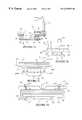
- FIG. 1is a schematic cross sectional view of a probe card constructed in accordance with the invention, mounted to a probe card fixture and illustrated during testing of a semiconductor wafer;
- FIG. 2is a bottom view, with the wafer partially cut away, of the probe card shown in FIG. 1;
- FIG. 3is an enlarged portion of FIG. 2 illustrating an interconnect substrate with patterns of contact members thereon, and a membrane for mounting the interconnect substrate to the probe card fixture;
- FIG. 3Ais an enlarged perspective view taken along section line 3 A— 3 A of FIG. 3, illustrating a single contact member with penetrating projections on the interconnect substrate;
- FIG. 3Bis an enlarged perspective view equivalent to FIG. 3A but illustrating an alternate embodiment contact member formed without penetrating projections;
- FIG. 3Cis a schematic plan view of an alternate embodiment interconnect substrate having sixteen patterns of contact members arranged in a single row;
- FIG. 4is an enlarged schematic cross sectional view taken along section line 4 — 4 of FIG. 1, illustrating a contact member for the interconnect in temporary electrical communication with a contact location on the semiconductor wafer;
- FIG. 4Ais an enlarged cross sectional view equivalent to FIG. 4, illustrating an alternate embodiment contact member adapted to test a “bumped” semiconductor wafer;
- FIG. 4Bis an enlarged cross sectional view equivalent to FIG. 4A, illustrating the alternate embodiment contact member for bumped wafers having a penetrating projection;
- FIG. 4Cis an enlarged cross sectional view equivalent to FIG. 4, illustrating another alternate embodiment contact member comprising a compliant spring segment;
- FIG. 4Dis an enlarged cross sectional view equivalent to FIG. 4, illustrating another alternate embodiment compliant contact member formed on an interconnect substrate;
- FIG. 5is a schematic cross sectional view illustrating the connection between the interconnect substrate, the membrane and the probe card fixture
- FIG. 5Ais a schematic cross sectional view equivalent to FIG. 5 but illustrating an alternate embodiment connection using a rigid mounting plate
- FIGS. 6A-6Care schematic cross sectional views illustrating an edge of the interconnect substrate and different electrical connections to conductors on the interconnect substrate;
- FIG. 7Ais a schematic cross sectional view illustrating the electrical path from the interconnect substrate to test circuitry for the probe card shown in FIG. 1;
- FIG. 7Bis a schematic cross sectional view illustrating an alternate mounting arrangement and electrical path to test circuitry for the interconnect substrate
- FIG. 7Cis a schematic cross sectional view illustrating another alternate embodiment mounting arrangement for the interconnect substrate, including a socket mounted to the probe card fixture and a mounting plate with terminal contacts;
- FIG. 7Dis a schematic cross sectional view illustrating another alternate embodiment mounting arrangement for the interconnect substrate including a leveling mechanism
- FIG. 7Eis a schematic cross sectional view illustrating another alternate embodiment mounting arrangement for the interconnect substrate including a leveling mechanism
- FIG. 7Fis a schematic cross sectional view taken along section line 7 F— 7 F of FIG. 7E;
- FIG. 8is a schematic block diagram illustrating a test system having a probe card constructed in accordance with the invention.
- FIGS. 9A-9Care enlarged schematic cross sectional views illustrating a fabrication process for the interconnect substrate shown in FIG. 1 .
- a probe card 10 constructed in accordance with the inventionis shown during testing of a semiconductor wafer 12 .
- the wafer 12includes a plurality of semiconductor dice 14 (FIG. 2) each having a plurality of contact locations 15 (FIG. 4 ).
- the contact locations 15are in electrical communication with the integrated circuits and semiconductor devices formed on the dice 14 and provide electrical access for testing.
- the wafer 12is supported circuit side up for contact with the probe card 10 .
- the wafer 12can be an entire semiconductor wafer 12 or portion of a wafer or other semiconducting substrate.
- a conventional testing apparatussuch as a wafer probe handler (not shown) can be used to support and bias the probe card 10 and wafer 12 together during the testing procedure.
- the wafer probe handlercan include a chuck (not shown) for supporting the wafer 12 . Suitable wafer probe handlers are manufactured by Electroglass and others.
- the probe card 10comprises an interconnect substrate 16 and a membrane 18 .
- the interconnect substrate 16includes patterns of contact members 20 configured to electrically contact the contact locations 15 (FIG. 4) on the semiconductor dice 14 .
- the membrane 18physically and electrically attaches the interconnect substrate 16 to a probe card fixture 22 mounted to the testing apparatus.
- a membrane mounting plate 24secures the membrane 18 to the probe card fixture 22 .
- the membrane mounting plate 24can be a rigid annular member that can be attached to the probe card fixture 22 using threaded fasteners 26 or other fastening mechanism.
- the membrane 18can be attached to the membrane mounting plate 24 using an adhesive (not shown) or threaded fasteners (not shown).
- the membrane mounting plate 24 and probe card fixture 22can be components of the wafer probe handler and are merely illustrative.
- a force applying mechanism 32 and spring loaded force applying member 34can be associated with the probe card fixture 22 .
- the interconnect substrate 16 and membrane 18can be mounted to other types of probe card fixtures.
- one type of other suitable probe card fixtureincludes a nest wherein the interconnect substrate 16 can be mounted.
- the probe card 10can also include a compressible member 28 in contact with a surface (e.g., backside) of the interconnect substrate 16 , and a pressure plate 30 in contact with the compressible member 28 .
- the compressible member 28 and pressure plate 30are configured to transfer pressure exerted by the force applying member 34 of the testing apparatus (e.g., wafer probe handler) to the interconnect substrate 16 .
- Thisprovides a contact force for forming the electrical connection between the contact members 20 and contact locations 15 (FIG. 4 ).
- the force applying member 34can be operated with less force.
- the interconnect substrate 16can be configured to test large groups of dice at the same time (e.g., 16, 32, 64, 128 etc.) up to all of the dice 14 on the wafer 12 .
- the pressure plate 30can be formed of metal or another rigid material in order to distribute the pressure across the full surface of the compressible member 28 .
- the compressible member 28can be formed of an elastomeric material to provide a cushioning effect.
- a metal filled elastomeric materialcan be used to provide heat conduction for cooling.
- the compressible member 28allows the contact members 20 to self planarize to the z-direction location of the contact locations 15 (FIG. 4) on the wafer 12 .
- the compressible member 28can be formed of an elastomeric material such as silicone, butyl rubber, or fluorosilicone; in foam, gel, solid or molded configurations. Suitable elastomeric materials include “PORON” available from Rogers or “BISCO” available from a Dow Chemical subsidiary.
- the compressible member 28 and pressure plate 30can have peripheral outlines that correspond to a peripheral outline of the interconnect substrate 16 .
- a representative thickness for the compressible member 28can be from 0.5 mm to 4 mm.
- the compressible member 28can be secured to the interconnect substrate 16 and pressure plate 30 using an adhesive such as silicone.
- One suitable adhesiveis “ZYMET” silicone elastomer manufactured by Zymet, Inc., East Hanover, N.J.
- the compressible member 28can be formed as a compressible gas filled bladder. This type of bladder is available from Paratech of Frankfort, Ill. under the trademark “MAXI FORCE AIR BAG”.
- the compressible member 28can also be formed as a heat conductive material such as a metal filled elastomer to conduct heat from the wafer.
- each contact member 20 on the interconnect substrate 16can be in electrical communication with a conductor 36 formed on the interconnect substrate 16 .
- the conductors 36 on the interconnect substrate 16can be physically and electrically bonded to corresponding conductors 38 formed on the membrane 18 .
- the conductors 38 on the membrane 18can be in electrical communication with contact plugs 40 (FIG. 1) formed on the probe card fixture 22 .
- the contact plugs 40 on the probe card fixture 22can be adapted for electrical contact by pogo pins 42 (FIG. 1) or other electrical connectors in electrical communication with test circuitry 44 (FIG. 1 ).
- the contact members 20 on the interconnect substrate 16are formed in patterns 46 that match the patterns of the contact locations 15 (FIG. 4) on the semiconductor dice 14 (FIG. 2 ).
- the wafer probe handlercan be used to step the wafer 12 , or the interconnect substrate 16 , so that the remaining dice 14 can be tested in groups of twelve (or less) until all of the dice 14 on the wafer 12 have been tested.
- FIG. 3Cillustrates an alternate embodiment interconnect substrate 16 C having sixteen patterns 46 of contact members 20 .
- the patterns 46are formed in a single row.
- patterns 46 of contact members 20are also possible.
- the patterns 46 of contact members 20 (FIG. 3) on the interconnect substrate 16must exactly match the patterns of contact locations 15 on the dice 14 .
- the stepping distancei.e., x-y repeat and pattern spacing
- the software that controls the stepping processmust be able to pick valid test sites. For example, when testing at the edges of a round wafer with a probe card that includes rectangular or square patterns of contact members 46 , some patterns of contact members 46 will not have an associated die under test. It is also desirable to not have contact members 46 contacting the passivation layer on the dice 14 as this can damage the contact members 20 .
- the interconnect substrate 16can be formed with enough patterns 46 of contact members 20 to simultaneously contact every contact location 15 for all of the dice 14 on the wafer 12 . Test signals can then be selectively applied and electronically switched as required, to selected dice 14 on the wafer 12 .
- the interconnect substrate 16can be formed with any desired number of patterns 46 of contact members 20 .
- the interconnect substrate 16can be configured to test a complete semiconductor wafer 12 or to test a partial wafer or other substrate that has been segmented into arrays of dice 14 .
- the contact members 20can be formed as raised members that project from a surface of the interconnect substrate 16 .
- the raised contact members 20help to provide a separation distance between the interconnect substrate 16 and the wafer 12 to clear any particulate contaminants that may be present on the opposing surfaces.
- the contact members 20can include penetrating projections 48 adapted to penetrate the contact locations 15 (FIG. 4) on the wafer 12 to a limited penetration depth.
- the penetrating projections 48have a height that is less than a thickness of the contact locations 15 (FIG. 4 ). For thin film aluminum contact locations 15 (FIG. 4) this thickness will typically be less than 2.0 ⁇ m.
- FIG. 4For thin film aluminum contact locations 15 (FIG. 4) this thickness will typically be less than 2.0 ⁇ m.
- an upper surface 50 of the contact member 20provides a stop plane for limiting penetration of the contact members 20 into the contact locations 15 (FIG. 4 ).
- This stop planealong with the dimensions of the penetrating projections 48 insures that the contact members 20 minimally damage the bond pads 16 during a test procedure.
- an alternate embodiment contact member 20 Ccan be formed without penetrating projections. In this case surfaces 50 C of the contact members 20 C contact but do not penetrate into the contact locations 15 (FIG. 4 ).
- the contact members 20 and penetrating projections 48can be formed integrally on the interconnect substrate 16 using a semiconductor fabrication process such as bulk micromachining. Such a process permits the contact members 20 and penetrating projections 48 to be formed accurately in a dense array.
- the interconnect substrate 16can be formed of silicon such that the CTE of the interconnect substrate 16 and wafer 12 can be the same.
- Each contact member 20includes a conductive layer 52 formed thereon.
- the interconnect substrate 16includes an insulating layer 54 formed over its entire surface.
- the insulating layer 54electrically insulates the conductive layers 52 for the contact members 20 and the conductors 36 from the interconnect substrate 16 .
- the insulating layer 54can be a grown or deposited oxide such as SiO 2 .
- the interconnect substrate 16can also be formed of doped silicon such that the bulk substrate functions as a ground plane (Vss). Such a ground plane can provide lower capacitance and impedance matching for high speed testing with less noise.
- the conductive layers 52 for all of the contact members 20can be formed of a metal layer deposited and patterned to cover the contact members 20 , or other selected areas of the interconnect substrate 18 .
- the conductive layers 52 for the contact members 20can be formed of aluminum, copper, titanium, tungsten, tantalum, platinum, molybdenum, cobalt, nickel, gold, iridium or alloys of these metals. Some of these materials such as gold and platinum are non-reactive so that material transfer between the contact members 20 and contact locations 15 can be minimized.
- the conductive layers 52can also be a metal silicide or a conductive material such as polysilicon.
- the conductive layers 52can be formed as a bi-metal stack comprising a base layer and a non-reactive and oxidation resistant outer layer such as gold or platinum.
- the conductive layers 52can be formed using a metallization process comprising deposition (e.g., CVD), followed by photo patterning and etching.
- the conductive layer 52 for each contact member 20is in electrical communication with a corresponding conductor 36 formed on the interconnect substrate 18 .
- the conductive layers 52 and conductors 36can be formed at the same time using the same metallization process. Alternately, the conductive layers 52 can be formed of a different metal than the conductors 36 using separate metallization process.
- the conductors 36can include bonding pads 56 formed at a terminal end thereof such as along a peripheral edge 57 of the interconnect substrate 16 .
- the peripheral edge 57can include a step (or groove) for recessing the bonding pads 56 to provide clearance for bonding to the membrane 18 .
- the bonding pads 56can be formed of a same metal as the conductors 36 or can be one or more different layers having a metallurgy suitable for soldering or otherwise forming an electrical interconnection to the conductors 38 on the membrane 18 . Further details of the electrical interconnection between the interconnect substrate 16 and the membrane 18 will become more apparent as the description proceeds.
- an alternate embodiment interconnect substrate 16 Bincludes indentation contact members 20 B for making electrical connections to a wafer with bumped contact locations 15 B.
- the bumped contact locations 15 Bwill typically be solder bumps bonded to a thin film bond pad.
- Conventionally formed solder bumps on a bumped die 14 Bhave a diameter of from 1 mils to 60 mils. Accordingly, the indentation contact members 46 A can be formed with an inside diameter of from 0.25 to 20 mils.
- the interconnect substrate 16 Bcan be formed of either silicon or ceramic. With a silicon substrate an insulating layer 54 B as previously described is required.
- the indentation contact members 20 Bcan be formed by etching or laser ablating concave depressions in the interconnect substrate 16 B, and then forming conductive layers 38 B on the depressions substantially as previously described for conductive layers 38 .
- the conductive layers 38 B for the indentation contact members 20 Bcan be formed in electrical communication with corresponding conductors 52 B as previously described.
- the indentation contact member 20 Bcan also include a penetrating projection 48 B for penetrating the bumped contact location 15 B to a limited penetration depth.
- the indentationcan be omitted and the penetrating projection 48 B can be formed directly on the surface of the interconnect substrate 16 B
- an alternate embodiment interconnect substrate 16 Sincludes compliant contact member 20 S for making electrical connections to the contact locations 15 (FIG. 4) previously described.
- the compliant contact member 20 Scan comprise a spring segment 74 and a ball contact 76 .
- the spring segment 74permits the compliant contact member 20 S to flex to accommodate variations in the locations of the contact locations 15 .
- the compliant contact members 20 Scan be attached to conductors 36 S formed on the interconnect substrate 16 S as previously described for conductor 36 (FIG. 4 ).
- the complaint contact member 20 Scan be formed by wire bonding or welding a metal wire to the conductor 36 S. During the wire bonding or welding process, the wires can be shaped to form the spring segments 74 and ball contacts 76 .
- the spring contact members 20 Srather than including spring segments can also be elongated pins that are angled with respect to the substrate 16 S to provide flexure or compliancy.
- an indentation contact member 20 Dcan also comprise a conductive layer 20 D plated directly on an interconnect substrate 16 D.
- the interconnect substrate 16 Dcan be formed of ceramic or other insulating material.
- depressionscan be formed in the interconnect substrate 16 D by etching or laser machining.
- the membrane 18functions to physically attach the interconnect substrate 16 to the membrane mounting plate 24 and probe card fixture 22 .
- the membrane 18functions to provide electrical paths between the contact members 20 and the test circuitry 44 (FIG. 1 ).
- the membrane 18can be formed of thin flexible materials to allow movement of the interconnect substrate 16 in z-directions. Additionally, the membrane 18 can be formed of materials to provide electrical insulation for the electrical paths.
- the membrane 18can be formed of a flexible multi layered material similar to TAB tape.
- TAB tapeis commercially available from manufacturers such as 3M, Shinko and Packard Hughes.
- the membrane 18comprises a layer of polymer tape 60 (FIG. 7A) formed of polyimide or other elastomeric material.
- the conductors 38 (FIG. 7A) on the membrane 18comprise a metal foil, such as copper, patterned as required and laminated to the polymer tape 60 (FIG. 7 A).
- the membrane 18is bonded directly to the interconnect 16 .
- the membrane 18can be attached to the membrane mounting plate 24 , which can be attached to the probe card fixture 22 .
- the membrane 18can be attached or laminated to the membrane mounting plate 24 using an adhesive.
- the membrane mounting plate 24can be formed as an annular shaped member, out of a rigid, electrically insulating, material such as a glass filled plastic (e.g., FR-4).
- the membrane 18overhangs from an edge 62 of the membrane mounting plate 24 .
- FIG. 5Aan alternate embodiment mounting arrangement for the interconnect substrate 16 is illustrated.
- the membrane 18is bonded to a mounting plate 80 and the interconnect substrate 16 is attached to the mounting plate 80 .
- the mounting plate 80can be formed of an electrically insulating material such as ceramic, or FR-4.
- the mounting plate 80can include patterns of conductors (not shown) for electrically connecting to the membrane 18 .
- wires 86can be wire bonded to conductors on the mounting plate 80 and to the bonding pads 56 (FIG. 4) on the interconnect 16 to form electrical paths therebetween.
- the conductors 38 on the membrane 18can include metal microbumps 58 formed in vias through the polymer tape 60 and arranged in a desired pattern.
- the metal microbumps 58can be formed of a heat bondable metal such as solder. This permits the metal microbumps 58 to be bonded, using heat or ultrasound, to the bonding pads 56 on the conductors 36 for the interconnect substrate 16 to form an electrical connection therebetween.
- the edge 57 of the interconnect substrate 16is stepped or grooved so that the contact members 20 can contact the contact locations 15 (FIG. 4) without interference from the metal microbumps 58 .
- the membrane 18can have a thickness of several mils or more the stepped edge 57 must recess the membrane from the contact members 20 by at least the same amount.
- the stepped edge 57can be formed by etching the substrate.
- the conductors 36 for the interconnect substrate 16can be formed over the stepped edge 57 .
- the electrical connection between the interconnect substrate 16 and membrane 18can be formed by a conductive adhesive 59 such as a z-axis anisotropic adhesive.
- the conductive adhesive 59can be deposited and cured to provide electrical communication between the bonding pads 56 on the interconnect substrate 16 and the conductors 38 on the membrane 18 .
- the electrical connection between the interconnect substrate 16 and membrane 18can be formed by a metal bump 61 bonded to the bonding pads 56 and the conductors 38 .
- a metal bump 61is gold.
- the membrane mounting plate 24can include electrically conductive contact plugs 72 (or vias) in electrical communication with the conductors 38 on the membrane 18 .
- the contact plugs 72 on the membrane mounting plate 24can be placed in electrical communication with metal microbumps 64 on the probe card fixture 22 .
- the metal microbumps 64can be formed on conductors 68 of TAB tape 66 attached to the probe card fixture 22 .
- the conductors 68 on the TAB tape 66can be in electrical connection with the contact plugs 40 on the probe card fixture 22 .
- the contact plugs 40 on the probe card fixture 22can be configured for electrical contact with pogo pins 42 or other electrical connectors in electrical communication with the test circuitry 44 .
- the probe card fixture 22can include an annular recess 70 (FIG. 4) to allow flexure of the TAB tape 66 relative to the probe card fixture 22 .
- the electrical path to and from the contact locations 15 (FIG. 4) on the dice 14 to the test circuitry 44 (FIG. 7A)is through the conductive layer 52 (FIG. 6A) on the contact members 20 , through the conductors 36 (FIG. 6A) on the interconnect substrate 16 (FIG. 6 A), through the metal microbumps 58 (FIG. 7A) on the membrane 18 , through the conductors 38 (FIG. 7A) on the membrane 18 , through the contact plugs 72 (FIG. 7A) on the membrane mounting plate 24 , through the microbump 64 (FIG. 7A) on the TAB tape 66 (FIG. 7 A), through the conductors 68 (FIG.
- the test circuitry 44is configured to apply test signals to test the operability of the integrated circuits on the dice 14 .
- FIG. 7Billustrates another mounting arrangement and exemplary electrical path to test circuitry 44 .
- the interconnect substrate 16is mounted to a mounting plate 80 LP and compressible member 28 substantially as previously described for mounting plate 80 .
- a membrane 18 Aphysically mounts the mounting plate 80 LP to the probe card fixture 22 (FIG. 1 ).
- the mounting plate 80 LPcan include land pads 40 LP arranged in a land grid array (LGA).
- the land pads 40 LPcan also include ball contacts (not shown) attached thereto to form a ball grid array (BGA).
- the land pads 40 LPare in electrical communication with internal conductors 90 formed within the mounting plate 80 LP.
- the mounting plate 80 LPcan be formed of laminated ceramic layers and the internal conductors 90 can be embedded in the ceramic layers.
- the conductors 90can include bonding pads (not shown) for wire bonding to the bond wires 86 .
- Pogo pins 42 in electrical communication with the test circuitry 44are adapted to contact the land pads 40 LP to form an electrical path for testing.
- the compressible member 28can be eliminated and the interconnect substrate 16 mounted directly to the mounting plate 80 LP.
- FIG. 7Cillustrates a mounting plate 80 PG having external contacts comprising pin contacts 40 PG arranged in a pin grid array (PGA).
- the mounting plate 80 PGis adapted to plug into a socket 92 mounted to the probe card fixture 22 (FIG. 1) or other component of the testing apparatus (e.g., wafer probe handler).
- the socket 92can be bonded to a membrane 18 B in electrical communication with the test circuitry 44 substantially as previously described.
- the socket 92can include a lever 94 for latching the pin contacts 40 PG with mating members on the socket 92 using latching mechanisms constructed using techniques that are known in the art.
- the compressible member 28can be mounted between the socket 92 and the probe card fixture 22 (FIG. 1 ).
- the mounting plate 80 PGcan be formed in other standard semiconductor packaging arrangements such as dual in line package (DIP), zig-zag in line package (ZIP), land grid array (LGA) or ball grid array (BGA).
- DIPdual in line package
- ZIPzig-zag in line package
- LGAland grid array
- BGAball grid array
- FIG. 7Dillustrates a mounting plate 80 A for the interconnect substrate 16 that is mounted to an air cushion fixture 96 .
- the air cushion fixture 96includes a sealed space 100 in flow communication with a gas supply 102 (e.g., compressed air).
- the air cushion fixture 96can include a gas conduit or can be formed of a porous material such as ceramic diffusion stone to permit gas flow to the sealed space 100 .
- the interconnect substrate 16is slidably mounted to the air cushion fixture 96 such that gas pressure in the sealed space 100 provides a desired force for biasing the interconnect substrate 16 against the wafer 12 (FIG. 1 ).
- the gas pressure within the sealed space 100can be controlled to exert a desired biasing force against the interconnect substrate 16 .
- the gascan be heated or cooled as required to provide a desired temperature for a testing procedure.
- a stop member 98can be formed on the air cushion fixture 96 to limit axial movement of the interconnect substrate 16 .
- the electrical connection to the test circuitry 44can be through a membrane 18 C bonded to the mounting plate 80 A and test circuitry 44 substantially as previously described.
- a leveling mechanism 104can be mounted to the probe card fixture 22 (FIG. 1) for leveling the air cushion fixture 96 with respect to the wafer 12 (FIG. 1) The leveling mechanism 104 attaches to the probe card fixture 22 substantially as previously described for force applying mechanism 32 .
- the leveling mechanism 104can include three or more leveling screws 106 and optionally leveling springs 108 for leveling the air cushion fixture 96 .
- the leveling mechanism 104can also include leveling shims (not shown).
- FIGS. 7E and 7Fillustrate another leveling mechanism 104 A.
- the leveling mechanism 104 Acan attaches to probe card fixture 22 substantially as previously described for force applying mechanism 32 (FIG. 1 ).
- a membrane 18 Dphysically and electrically connects the interconnect substrate 16 to test circuitry 44 substantially as previously described.
- the leveling mechanism 104 Aincludes a leveling plate 110 and leveling screws 106 A.
- three leveling screws 106 Aare arranged in a triangular pattern and threadably engage mating threaded openings in the leveling mechanism 104 A.
- the leveling screws 106 Apermit the planarity of the contact members 20 to be adjusted with respect to a plane of the wafer 12 (FIG. 1 ).
- the interconnect substrate 16can be easily installed or replaced as required, without requiring the probe handler chuck to be replanarized.
- the leveling screws 106 Acan be pivotably mounted to the leveling mechanism 104 A using ball joints (not shown) or similar members.
- the system 82includes a testing apparatus 78 in the form of a conventional wafer probe handler or similar apparatus.
- a testing apparatus 78is in electrical communication with or includes the test circuitry 44 .
- the test circuitry 44is adapted to send and receive test signals 84 for testing the integrated circuits on the wafer 12 .
- the testing apparatus 78can also include an optical or mechanical alignment system for aligning the contact locations 15 (FIG. 4) on the wafer 12 to the contact members 20 on the interconnect substrate 16 .
- testing apparatus 78can include the pogo pins 42 in the conductive path from the test circuitry 44 .
- the testing apparatus 78can also include the probe card fixture 22 .
- the testing apparatus 78can include the force applying mechanism 32 for applying pressure to bias the interconnect substrate 16 against the wafer 12 .
- the probe card 10includes the membrane 18 and the interconnect substrate 16 .
- the membrane 18can be attached to the probe card fixture 22 as previously described.
- the interconnect substrate 16can be attached to the membrane 18 also as previously described.
- the contact members 20 on the interconnect substrateare configured to penetrate the contact locations 15 , on the wafer 12 to a limited penetration depth.
- the interconnect substrate 16comprises silicon or other etchable semiconductor material.
- the penetrating projections 48can be formed by forming a mask (not shown) on the substrate 16 and then etching exposed portion of the substrate 16 through the mask.
- a hard maskcan be formed on the substrate 16 by depositing a layer of silicon nitride (Si 3 N 4 ) and then patterning the silicon nitride layer using hot phosphoric acid.
- a wet or dry, isotropic or anisotropic, etch processcan then be used to etch through openings in the hard mask to form the projections 48 .
- an anisotropic etchcan be performed on a substrate 16 formed of silicon using a solution of KOH and H 2 O. This type of semiconductor fabrication process is sometimes referred to as “bulk micromachining”.
- the projections 48can be elongated blades or sharp points formed in locations that match the placement of the contact locations 15 (FIG. 4) on the dice 14 .
- a greater or lesser number of projections 48can be formed.
- the projections 48 for each contact member 20are formed in a pattern having an outline contained within the perimeter of the contact locations 15 (FIG. 4) on the dice 14 .
- a representative height for the projections 48 measured from the base to the tipcan be from 0.1 to 1 ⁇ m.
- a representative length for the projections 48 measured from end to endcan be from 3 to 10 ⁇ m.
- the size of the projections 48(e.g., 100-10,000 ⁇ ) insures that the projections do not penetrate through the contact locations 15 (FIG. 4 ), which are typically about 2000 to 15,000 ⁇ thick.
- surface 50 (FIG. 9C) on the contact members 16provide a stop plane to limit the penetration depth.
- the hard maskcan be stripped and another mask (not shown) can be formed for etching the substrate 16 to form the contact members 20 .
- the contact members 20can be formed as topographically elevated pillars generally conical in shape.
- a representative height of the contact members 20 from base to tipcan be from 10-100 ⁇ m.
- the contact members 20thus have a height that is from 10 to 1000 times greater than the height of the penetrating projections 48 .
- a representative width of each side of the contact members 20can be from 40-80 ⁇ m.
- the contact members 20separate the interconnect substrate 16 from the wafer 12 with a clearance distance equal to the height of the contact members 20 (e.g., 10-100 ⁇ m). This separation distance functions to clear particulate contaminants on the opposing surfaces that could cause shorting. The separation distance also functions to diminish cross talk between the wafer 12 and the interconnect substrate 16 during the test procedure. Following formation of the contact members 20 , the etch mask can be stripped.
- Suitable etch processes for forming the contact members 20 and projections 16 substantially as shown in FIG. 9Aare also disclosed in U.S. Pat. Nos. 5,326,428; 5,419,807 and 5,483,741 which are incorporated herein by reference.
- the peripheral edges of the interconnect substrate 16can be etched to form the stepped edge 57 .
- the stepped edge 57forms a shelf wherein the bonding pads 56 will be formed. The shelf helps to provide a clearance space for bonding the membrane 18 to the interconnect substrate 16 .
- the insulating layer 54can be formed over the entire interconnect substrate 16 including over the contact members 20 and projections 48 .
- the insulating layer 54can be a grown or deposited material such as SiO 2 or Si 3 N 4 .
- a representative thickness for the insulating layer 54can be from 500 ⁇ to 1 ⁇ m.
- the conductive layers 52 for the contact members 20can be formed on the insulating layer 54 .
- the conductive layers 52 for all of the contact members 20can be a same layer of material that has been patterned to cover just the contact members 20 and selected portions of the substrate 16 .
- a highly conductive metalcan be blanket deposited on the substrate 16 by sputtering or other deposition process. Exemplary metals include aluminum, platinum, palladium, copper, gold and silver or alloys of these metals.
- a representative thickness for the conductive layers 52can be from 500 ⁇ to 2 ⁇ m.
- the conductive layers 52can also comprise a bi-metal stack comprising a base layer and a non-reactive outer layer.
- a resist maskcan be formed and used for etching the conductive metal such that at least a portion of the contact members 20 remain covered with the conductive layers 52 .
- the resist maskcan be deposited using a standard photoresist deposition and exposure process. This can include spin deposition, followed by hardening, exposure and development.
- U.S. patent application Ser. No. 08/520,871 now, U.S. Pat. No. 5,607,818 incorporated herein by referencedescribes a method for patterning a conductive layer using an electrophoretically deposited layer of resist.
- the conductive layers 52can be formed as a metal silicide using a process as disclosed in U.S. Pat. No. 5,483,741 incorporated herein by reference.
- the conductors 36 and bonding pads 56can also be formed in electrical communication with the conductive layers 52 using the same material and metallization process used to form the conductive layers 52 .
- the conductors 36can follow the contour of the stepped edge 57 .
- the conductors 36 and bonding pads 56can also be formed using different materials and different metallization processes.
- the conductors 36 and bonding pads 56can be formed using a process such as plating, thin film deposition or screen printing.
- the conductors 36can be insulated with a layer of material such as polyimide (not shown).
- the inventionprovides an improved probe card for testing semiconductors wafers, a method for testing semiconductor wafers using the probe card, and a system for testing using the probe card.
- the probe cardcan include contact members formed on a silicon interconnect such that a CTE with the wafer is matched.
- contact memberscan be formed on the interconnect in dense arrays to accommodate testing of dense arrays of dice having dense contact locations. Another advantage is that the contact members can be used to repeatedly test wafers without requiring adjustment for damage or wear as with conventional probe cards. Still further, because the contact members can be made very small, the size of the contact locations on the wafer can also be made very small. This can allow the size of the dice on the wafer to be smaller.
Landscapes
- Physics & Mathematics (AREA)
- General Physics & Mathematics (AREA)
- Engineering & Computer Science (AREA)
- Computer Hardware Design (AREA)
- Microelectronics & Electronic Packaging (AREA)
- General Engineering & Computer Science (AREA)
- Testing Or Measuring Of Semiconductors Or The Like (AREA)
- Measuring Leads Or Probes (AREA)
- Testing Of Individual Semiconductor Devices (AREA)
- Mechanical Treatment Of Semiconductor (AREA)
Abstract
Description
Claims (25)
Priority Applications (4)
| Application Number | Priority Date | Filing Date | Title |
|---|---|---|---|
| US09/303,367US6275052B1 (en) | 1997-02-11 | 1999-04-30 | Probe card and testing method for semiconductor wafers |
| US09/929,388US6359456B1 (en) | 1997-02-11 | 2001-08-14 | Probe card and test system for semiconductor wafers |
| US10/072,734US6798224B1 (en) | 1997-02-11 | 2002-02-05 | Method for testing semiconductor wafers |
| US10/742,729US7250780B2 (en) | 1997-02-11 | 2003-12-19 | Probe card for semiconductor wafers having mounting plate and socket |
Applications Claiming Priority (2)
| Application Number | Priority Date | Filing Date | Title |
|---|---|---|---|
| US08/797,719US6060891A (en) | 1997-02-11 | 1997-02-11 | Probe card for semiconductor wafers and method and system for testing wafers |
| US09/303,367US6275052B1 (en) | 1997-02-11 | 1999-04-30 | Probe card and testing method for semiconductor wafers |
Related Parent Applications (1)
| Application Number | Title | Priority Date | Filing Date |
|---|---|---|---|
| US08/797,719DivisionUS6060891A (en) | 1997-02-11 | 1997-02-11 | Probe card for semiconductor wafers and method and system for testing wafers |
Related Child Applications (1)
| Application Number | Title | Priority Date | Filing Date |
|---|---|---|---|
| US09/929,388DivisionUS6359456B1 (en) | 1997-02-11 | 2001-08-14 | Probe card and test system for semiconductor wafers |
Publications (1)
| Publication Number | Publication Date |
|---|---|
| US6275052B1true US6275052B1 (en) | 2001-08-14 |
Family
ID=25171622
Family Applications (3)
| Application Number | Title | Priority Date | Filing Date |
|---|---|---|---|
| US08/797,719Expired - LifetimeUS6060891A (en) | 1997-02-11 | 1997-02-11 | Probe card for semiconductor wafers and method and system for testing wafers |
| US09/303,367Expired - LifetimeUS6275052B1 (en) | 1997-02-11 | 1999-04-30 | Probe card and testing method for semiconductor wafers |
| US09/929,388Expired - Fee RelatedUS6359456B1 (en) | 1997-02-11 | 2001-08-14 | Probe card and test system for semiconductor wafers |
Family Applications Before (1)
| Application Number | Title | Priority Date | Filing Date |
|---|---|---|---|
| US08/797,719Expired - LifetimeUS6060891A (en) | 1997-02-11 | 1997-02-11 | Probe card for semiconductor wafers and method and system for testing wafers |
Family Applications After (1)
| Application Number | Title | Priority Date | Filing Date |
|---|---|---|---|
| US09/929,388Expired - Fee RelatedUS6359456B1 (en) | 1997-02-11 | 2001-08-14 | Probe card and test system for semiconductor wafers |
Country Status (6)
| Country | Link |
|---|---|
| US (3) | US6060891A (en) |
| EP (3) | EP1018023B1 (en) |
| AT (1) | ATE294396T1 (en) |
| AU (1) | AU6662998A (en) |
| DE (1) | DE69829986T2 (en) |
| WO (1) | WO1998035238A1 (en) |
Cited By (39)
| Publication number | Priority date | Publication date | Assignee | Title |
|---|---|---|---|---|
| US20020025603A1 (en)* | 1998-12-04 | 2002-02-28 | Douglas S. Ondricek | Method for mounting an electronic component |
| US6356098B1 (en) | 1998-02-23 | 2002-03-12 | Micron Technology, Inc. | Probe card, test method and test system for semiconductor wafers |
| US6380555B1 (en) | 1999-12-24 | 2002-04-30 | Micron Technology, Inc. | Bumped semiconductor component having test pads, and method and system for testing bumped semiconductor components |
| US6419844B1 (en) | 1998-05-26 | 2002-07-16 | Micron Technology, Inc. | Method for fabricating calibration target for calibrating semiconductor wafer test systems |
| US6433574B1 (en) | 1998-05-11 | 2002-08-13 | Micron Technology, Inc. | Interconnect and system for testing bumped semiconductor components with on-board multiplex circuitry for expanding tester resources |
| US6469537B1 (en) | 1997-02-24 | 2002-10-22 | Micron Technology, Inc. | System for testing semiconductor wafers having interconnect with pressure sensing mechanism |
| US6498503B2 (en) | 1996-04-01 | 2002-12-24 | Micron Technology, Inc. | Semiconductor test interconnect with variable flexure contacts |
| US20020197895A1 (en)* | 1999-08-17 | 2002-12-26 | Formfactor, Inc. | Electrical contractor, especially wafer level contactor, using fluid pressure |
| US6522018B1 (en) | 2000-05-16 | 2003-02-18 | Micron Technology, Inc. | Ball grid array chip packages having improved testing and stacking characteristics |
| US6545493B1 (en)* | 1999-09-29 | 2003-04-08 | Tokyo Electron Limited | High-speed probing apparatus |
| US6563215B1 (en) | 2000-01-10 | 2003-05-13 | Micron Technology, Inc. | Silicon carbide interconnect for semiconductor components and method of fabrication |
| US20030117162A1 (en)* | 2001-12-21 | 2003-06-26 | Watts Stephen M. | Parallel integrated circuit test apparatus and test method |
| US6600334B1 (en) | 1997-12-31 | 2003-07-29 | Micron Technology, Inc. | Force applying probe card and test system for semiconductor wafers |
| FR2836721A1 (en)* | 2002-03-04 | 2003-09-05 | Probest | Multiple connection device for testing of microelectronic circuits, such as chips used in microcomputers and photosensitive cells, said device operating over a wide temperature range with varied electronic circuits |
| US20030221152A1 (en)* | 2002-05-24 | 2003-11-27 | Volkerink Erik H. | System and method for testing circuitry on a wafer |
| US6670818B1 (en) | 1997-11-24 | 2003-12-30 | Micron Technology, Inc. | Method for aligning and connecting semiconductor components to substrates |
| US6677776B2 (en) | 1998-05-11 | 2004-01-13 | Micron Technology, Inc. | Method and system having switching network for testing semiconductor components on a substrate |
| US6696850B1 (en) | 2002-10-02 | 2004-02-24 | Interconnect Devices, Inc. | Contact probe with off-centered back-drilled aperture |
| US20040100778A1 (en)* | 2002-11-25 | 2004-05-27 | Patrizio Vinciarelli | Power converter package and thermal management |
| US20040132222A1 (en)* | 1997-02-11 | 2004-07-08 | Hembree David R. | Probe card for semiconductor wafers and method and system for testing wafers |
| US20040174176A1 (en)* | 2003-03-06 | 2004-09-09 | Kirby Kyle K. | Semiconductor interconnect having semiconductor spring contacts, test systems incorporating the interconnect and test methods using the interconnect |
| US20050012221A1 (en)* | 2003-07-14 | 2005-01-20 | Kirby Kyle K. | Semiconductor interconnect having conductive spring contacts, method of fabrication, and test systems incorporating the interconnect |
| US6897670B2 (en) | 2001-12-21 | 2005-05-24 | Texas Instruments Incorporated | Parallel integrated circuit test apparatus and test method |
| US20050258845A1 (en)* | 2004-05-20 | 2005-11-24 | Wan-Chuan Chou | Pad type wafer test apparatus |
| US6975030B1 (en) | 2000-01-10 | 2005-12-13 | Micron Technology, Inc. | Silicon carbide contact for semiconductor components |
| US20060046345A1 (en)* | 2000-01-10 | 2006-03-02 | Salman Akram | Method for fabricating a silicon carbide interconnect for semiconductor components using heating and oxidizing |
| US20060084292A1 (en)* | 2004-10-20 | 2006-04-20 | Matsushita Electric Industrial Co., Ltd. | Switch and manufacturing method thereof |
| US7049840B1 (en) | 1997-03-21 | 2006-05-23 | Micron Technology, Inc. | Hybrid interconnect and system for testing semiconductor dice |
| US7064564B2 (en)* | 2001-02-01 | 2006-06-20 | Antares Contech, Inc. | Bundled probe apparatus for multiple terminal contacting |
| US7148713B1 (en) | 2005-10-28 | 2006-12-12 | Interconnect Devices, Inc. | Algoristic spring as probe |
| US20070268031A1 (en)* | 2006-05-18 | 2007-11-22 | Centipede Systems, Inc. | Wafer Probe Interconnect System |
| US7355423B2 (en) | 2006-05-24 | 2008-04-08 | Micron Technology, Inc. | Method for optimizing probe card design |
| US7396236B2 (en) | 2001-03-16 | 2008-07-08 | Formfactor, Inc. | Wafer level interposer |
| US20080196474A1 (en)* | 2007-02-20 | 2008-08-21 | Centipede Systems, Inc. | Method and apparatus for aligning and/or leveling a test head |
| US20090068858A1 (en)* | 2007-08-17 | 2009-03-12 | Centipede Systems, Inc. | Miniature electrical ball and tube socket assembly with self-capturing multiple-contact-point coupling |
| US20130093453A1 (en)* | 2010-08-17 | 2013-04-18 | Advantest Corporation | Connecting device, semiconductor wafer test apparatus comprising same, and connecting method |
| WO2016195766A1 (en)* | 2015-05-29 | 2016-12-08 | R&D Circuits, Inc. | Improved power supply transient performance (power integrity) for a probe card assembly in an integrated circuit test environment |
| US11322473B2 (en) | 2019-09-12 | 2022-05-03 | International Business Machines Corporation | Interconnect and tuning thereof |
| US11561243B2 (en) | 2019-09-12 | 2023-01-24 | International Business Machines Corporation | Compliant organic substrate assembly for rigid probes |
Families Citing this family (107)
| Publication number | Priority date | Publication date | Assignee | Title |
|---|---|---|---|---|
| US6380751B2 (en) | 1992-06-11 | 2002-04-30 | Cascade Microtech, Inc. | Wafer probe station having environment control enclosure |
| US5345170A (en) | 1992-06-11 | 1994-09-06 | Cascade Microtech, Inc. | Wafer probe station having integrated guarding, Kelvin connection and shielding systems |
| IT1272653B (en)* | 1993-09-20 | 1997-06-26 | Alcatel Italia | NOISE REDUCTION METHOD, IN PARTICULAR FOR AUTOMATIC SPEECH RECOGNITION, AND FILTER SUITABLE TO IMPLEMENT THE SAME |
| US7064566B2 (en)* | 1993-11-16 | 2006-06-20 | Formfactor, Inc. | Probe card assembly and kit |
| US5561377A (en) | 1995-04-14 | 1996-10-01 | Cascade Microtech, Inc. | System for evaluating probing networks |
| US6232789B1 (en) | 1997-05-28 | 2001-05-15 | Cascade Microtech, Inc. | Probe holder for low current measurements |
| US20020004320A1 (en)* | 1995-05-26 | 2002-01-10 | David V. Pedersen | Attaratus for socketably receiving interconnection elements of an electronic component |
| US5914613A (en) | 1996-08-08 | 1999-06-22 | Cascade Microtech, Inc. | Membrane probing system with local contact scrub |
| US5952840A (en) | 1996-12-31 | 1999-09-14 | Micron Technology, Inc. | Apparatus for testing semiconductor wafers |
| US6060891A (en) | 1997-02-11 | 2000-05-09 | Micron Technology, Inc. | Probe card for semiconductor wafers and method and system for testing wafers |
| US6025730A (en) | 1997-03-17 | 2000-02-15 | Micron Technology, Inc. | Direct connect interconnect for testing semiconductor dice and wafers |
| US5962921A (en) | 1997-03-31 | 1999-10-05 | Micron Technology, Inc. | Interconnect having recessed contact members with penetrating blades for testing semiconductor dice and packages with contact bumps |
| US6002263A (en) | 1997-06-06 | 1999-12-14 | Cascade Microtech, Inc. | Probe station having inner and outer shielding |
| US6130148A (en) | 1997-12-12 | 2000-10-10 | Farnworth; Warren M. | Interconnect for semiconductor components and method of fabrication |
| US6181144B1 (en) | 1998-02-25 | 2001-01-30 | Micron Technology, Inc. | Semiconductor probe card having resistance measuring circuitry and method fabrication |
| US5933713A (en)* | 1998-04-06 | 1999-08-03 | Micron Technology, Inc. | Method of forming overmolded chip scale package and resulting product |
| US6246250B1 (en) | 1998-05-11 | 2001-06-12 | Micron Technology, Inc. | Probe card having on-board multiplex circuitry for expanding tester resources |
| US6256882B1 (en) | 1998-07-14 | 2001-07-10 | Cascade Microtech, Inc. | Membrane probing system |
| US6441315B1 (en)* | 1998-11-10 | 2002-08-27 | Formfactor, Inc. | Contact structures with blades having a wiping motion |
| JP3730428B2 (en)* | 1998-12-22 | 2006-01-05 | 富士通株式会社 | Manufacturing method of contactor for semiconductor device test |
| US6263566B1 (en) | 1999-05-03 | 2001-07-24 | Micron Technology, Inc. | Flexible semiconductor interconnect fabricated by backslide thinning |
| US6414500B1 (en)* | 1999-05-14 | 2002-07-02 | Mitsubishi Denki Kabushiki Kaisha | Test socket for an electronic circuit device having improved contact pins and manufacturing method thereof |
| US7247035B2 (en) | 2000-06-20 | 2007-07-24 | Nanonexus, Inc. | Enhanced stress metal spring contactor |
| US7382142B2 (en)* | 2000-05-23 | 2008-06-03 | Nanonexus, Inc. | High density interconnect system having rapid fabrication cycle |
| US6917525B2 (en)* | 2001-11-27 | 2005-07-12 | Nanonexus, Inc. | Construction structures and manufacturing processes for probe card assemblies and packages having wafer level springs |
| US6812718B1 (en) | 1999-05-27 | 2004-11-02 | Nanonexus, Inc. | Massively parallel interface for electronic circuits |
| US7349223B2 (en)* | 2000-05-23 | 2008-03-25 | Nanonexus, Inc. | Enhanced compliant probe card systems having improved planarity |
| US6578264B1 (en) | 1999-06-04 | 2003-06-17 | Cascade Microtech, Inc. | Method for constructing a membrane probe using a depression |
| US6445202B1 (en) | 1999-06-30 | 2002-09-03 | Cascade Microtech, Inc. | Probe station thermal chuck with shielding for capacitive current |
| US6657446B1 (en)* | 1999-09-30 | 2003-12-02 | Advanced Micro Devices, Inc. | Picosecond imaging circuit analysis probe and system |
| TW460697B (en)* | 2000-01-24 | 2001-10-21 | Urex Prec Inc | Probe card of thin film type |
| US6838890B2 (en) | 2000-02-25 | 2005-01-04 | Cascade Microtech, Inc. | Membrane probing system |
| TW494517B (en)* | 2000-03-17 | 2002-07-11 | Matsushita Electric Industrial Co Ltd | Method and apparatus for evaluating insulation film |
| US7579848B2 (en) | 2000-05-23 | 2009-08-25 | Nanonexus, Inc. | High density interconnect system for IC packages and interconnect assemblies |
| US7952373B2 (en) | 2000-05-23 | 2011-05-31 | Verigy (Singapore) Pte. Ltd. | Construction structures and manufacturing processes for integrated circuit wafer probe card assemblies |
| US6441629B1 (en)* | 2000-05-31 | 2002-08-27 | Advantest Corp | Probe contact system having planarity adjustment mechanism |
| FR2811084B1 (en)* | 2000-06-29 | 2002-10-25 | Bioalliance Pharma | METHOD FOR IDENTIFYING A FUNCTIONAL BIOLOGICAL CHARACTERISTIC OF A LIVING MATERIAL |
| US6965226B2 (en) | 2000-09-05 | 2005-11-15 | Cascade Microtech, Inc. | Chuck for holding a device under test |
| US6914423B2 (en) | 2000-09-05 | 2005-07-05 | Cascade Microtech, Inc. | Probe station |
| DE20114544U1 (en) | 2000-12-04 | 2002-02-21 | Cascade Microtech, Inc., Beaverton, Oreg. | wafer probe |
| US6553661B2 (en)* | 2001-01-04 | 2003-04-29 | Texas Instruments Incorporated | Semiconductor test structure having a laser defined current carrying structure |
| KR100428782B1 (en)* | 2001-04-11 | 2004-04-27 | 삼성전자주식회사 | Apparatus for measuring tension of pogo pin |
| US6912778B2 (en) | 2001-07-19 | 2005-07-05 | Micron Technology, Inc. | Methods of fabricating full-wafer silicon probe cards for burn-in and testing of semiconductor devices |
| US7355420B2 (en) | 2001-08-21 | 2008-04-08 | Cascade Microtech, Inc. | Membrane probing system |
| WO2003020467A1 (en) | 2001-08-31 | 2003-03-13 | Cascade Microtech, Inc. | Optical testing device |
| US6777964B2 (en) | 2002-01-25 | 2004-08-17 | Cascade Microtech, Inc. | Probe station |
| US7352258B2 (en)* | 2002-03-28 | 2008-04-01 | Cascade Microtech, Inc. | Waveguide adapter for probe assembly having a detachable bias tee |
| US6965244B2 (en) | 2002-05-08 | 2005-11-15 | Formfactor, Inc. | High performance probe system |
| KR100864916B1 (en) | 2002-05-23 | 2008-10-22 | 캐스케이드 마이크로테크 인코포레이티드 | Probes for Testing Devices Under Test |
| US6621710B1 (en)* | 2002-07-19 | 2003-09-16 | Chipmos Technologies (Bermuda) Ltd. | Modular probe card assembly |
| US6841991B2 (en)* | 2002-08-29 | 2005-01-11 | Micron Technology, Inc. | Planarity diagnostic system, E.G., for microelectronic component test systems |
| US6880350B2 (en)* | 2002-09-13 | 2005-04-19 | Isothermal Systems Research, Inc. | Dynamic spray system |
| US6857283B2 (en) | 2002-09-13 | 2005-02-22 | Isothermal Systems Research, Inc. | Semiconductor burn-in thermal management system |
| US6847219B1 (en) | 2002-11-08 | 2005-01-25 | Cascade Microtech, Inc. | Probe station with low noise characteristics |
| US6724205B1 (en) | 2002-11-13 | 2004-04-20 | Cascade Microtech, Inc. | Probe for combined signals |
| US7250779B2 (en) | 2002-11-25 | 2007-07-31 | Cascade Microtech, Inc. | Probe station with low inductance path |
| US6861856B2 (en) | 2002-12-13 | 2005-03-01 | Cascade Microtech, Inc. | Guarded tub enclosure |
| US6841883B1 (en)* | 2003-03-31 | 2005-01-11 | Micron Technology, Inc. | Multi-dice chip scale semiconductor components and wafer level methods of fabrication |
| US6984996B2 (en)* | 2003-05-01 | 2006-01-10 | Celerity Research, Inc. | Wafer probing that conditions devices for flip-chip bonding |
| US7221172B2 (en) | 2003-05-06 | 2007-05-22 | Cascade Microtech, Inc. | Switched suspended conductor and connection |
| US6781392B1 (en) | 2003-05-12 | 2004-08-24 | Chipmos Technologies Ltd. | Modularized probe card with compressible electrical connection device |
| US7057404B2 (en) | 2003-05-23 | 2006-06-06 | Sharp Laboratories Of America, Inc. | Shielded probe for testing a device under test |
| US7492172B2 (en) | 2003-05-23 | 2009-02-17 | Cascade Microtech, Inc. | Chuck for holding a device under test |
| DE20310622U1 (en)* | 2003-07-10 | 2003-11-06 | Seda S.P.A., Arzano | container |
| TWI351524B (en)* | 2003-07-28 | 2011-11-01 | Nextest Systems Corp | Apparatus for planarizing a probe card and method |
| JP2005055330A (en)* | 2003-08-06 | 2005-03-03 | Elpida Memory Inc | Pressure device for semiconductor device |
| US6924655B2 (en)* | 2003-09-03 | 2005-08-02 | Micron Technology, Inc. | Probe card for use with microelectronic components, and methods for making same |
| US6946860B2 (en)* | 2003-10-08 | 2005-09-20 | Chipmos Technologies (Bermuda) Ltd. | Modularized probe head |
| US7250626B2 (en) | 2003-10-22 | 2007-07-31 | Cascade Microtech, Inc. | Probe testing structure |
| WO2005065258A2 (en) | 2003-12-24 | 2005-07-21 | Cascade Microtech, Inc. | Active wafer probe |
| US7187188B2 (en) | 2003-12-24 | 2007-03-06 | Cascade Microtech, Inc. | Chuck with integrated wafer support |
| JP2005233858A (en)* | 2004-02-23 | 2005-09-02 | Japan Electronic Materials Corp | Probe card |
| JP2005241275A (en)* | 2004-02-24 | 2005-09-08 | Japan Electronic Materials Corp | Probe card |
| US7332921B2 (en)* | 2004-03-26 | 2008-02-19 | Cypress Semiconductor Corporation | Probe card and method for constructing same |
| WO2005121824A2 (en) | 2004-06-07 | 2005-12-22 | Cascade Microtech, Inc. | Thermal optical chuck |
| US7330041B2 (en) | 2004-06-14 | 2008-02-12 | Cascade Microtech, Inc. | Localizing a temperature of a device for testing |
| KR101157449B1 (en) | 2004-07-07 | 2012-06-22 | 캐스케이드 마이크로테크 인코포레이티드 | Probe head having a membrane suspended probe |
| US6979240B1 (en) | 2004-08-09 | 2005-12-27 | Kurt Barton | Adjustable foot pedestal for a trolling motor controller |
| EP1789812A2 (en) | 2004-09-13 | 2007-05-30 | Cascade Microtech, Inc. | Double sided probing structures |
| US7507099B2 (en)* | 2004-10-01 | 2009-03-24 | Teradyne, Inc. | Floating interface linkage |
| US7180318B1 (en)* | 2004-10-15 | 2007-02-20 | Xilinx, Inc. | Multi-pitch test probe assembly for testing semiconductor dies having contact pads |
| US7656172B2 (en) | 2005-01-31 | 2010-02-02 | Cascade Microtech, Inc. | System for testing semiconductors |
| US7535247B2 (en) | 2005-01-31 | 2009-05-19 | Cascade Microtech, Inc. | Interface for testing semiconductors |
| US7449899B2 (en) | 2005-06-08 | 2008-11-11 | Cascade Microtech, Inc. | Probe for high frequency signals |
| JP5080459B2 (en) | 2005-06-13 | 2012-11-21 | カスケード マイクロテック インコーポレイテッド | Wideband active / passive differential signal probe |
| US7609077B2 (en) | 2006-06-09 | 2009-10-27 | Cascade Microtech, Inc. | Differential signal probe with integral balun |
| US7532022B2 (en) | 2006-06-09 | 2009-05-12 | Advanced Inquiry Systems, Inc. | Apparatus for fixed-form multi-planar extension of electrical conductors beyond the margins of a substrate |
| US7403028B2 (en) | 2006-06-12 | 2008-07-22 | Cascade Microtech, Inc. | Test structure and probe for differential signals |
| US7443186B2 (en) | 2006-06-12 | 2008-10-28 | Cascade Microtech, Inc. | On-wafer test structures for differential signals |
| US7723999B2 (en) | 2006-06-12 | 2010-05-25 | Cascade Microtech, Inc. | Calibration structures for differential signal probing |
| US7764072B2 (en) | 2006-06-12 | 2010-07-27 | Cascade Microtech, Inc. | Differential signal probing system |
| DE102006035644A1 (en)* | 2006-07-31 | 2008-02-14 | Advanced Micro Devices, Inc., Sunnyvale | A method of reducing contamination by providing a polymeric protective layer to be removed during processing of microstructures |
| JP5049694B2 (en)* | 2007-08-07 | 2012-10-17 | ルネサスエレクトロニクス株式会社 | Probe card, semiconductor inspection apparatus, and semiconductor device manufacturing method |
| US7876114B2 (en) | 2007-08-08 | 2011-01-25 | Cascade Microtech, Inc. | Differential waveguide probe |
| JP5553480B2 (en)* | 2008-02-26 | 2014-07-16 | 株式会社日本マイクロニクス | Electrical connection device |
| US7888957B2 (en) | 2008-10-06 | 2011-02-15 | Cascade Microtech, Inc. | Probing apparatus with impedance optimized interface |
| US8410806B2 (en) | 2008-11-21 | 2013-04-02 | Cascade Microtech, Inc. | Replaceable coupon for a probing apparatus |
| US8319503B2 (en) | 2008-11-24 | 2012-11-27 | Cascade Microtech, Inc. | Test apparatus for measuring a characteristic of a device under test |
| US8251755B2 (en)* | 2010-06-14 | 2012-08-28 | Tyco Electronics Corporation | Connector with a laterally moving contact |
| TWI534432B (en) | 2010-09-07 | 2016-05-21 | 瓊斯科技國際公司 | Electrical conduction pins for microcircuit testers |
| US8797057B2 (en) | 2011-02-11 | 2014-08-05 | Taiwan Semiconductor Manufacturing Company, Ltd. | Testing of semiconductor chips with microbumps |
| WO2017210088A1 (en)* | 2016-05-31 | 2017-12-07 | Intercomp Company | Strip scale technology |
| KR102660264B1 (en)* | 2021-11-26 | 2024-04-25 | (주)티에스이 | Handling apparatus for thin film semiconductor device and semiconductor testing apparatus comprising the same |
| CN114200280B (en)* | 2021-11-29 | 2022-11-15 | 强一半导体(苏州)有限公司 | Film probe card and probe head thereof |
| CN116780224A (en)* | 2022-03-11 | 2023-09-19 | 星科金朋私人有限公司 | Test socket and apparatus for testing semiconductor packages |
| TWI868842B (en)* | 2023-08-04 | 2025-01-01 | 漢民測試系統股份有限公司 | Adjustable supporting device |
| KR102698565B1 (en)* | 2024-02-19 | 2024-08-23 | 서기복 | Probe head and substrate inspection device including the same |
Citations (37)
| Publication number | Priority date | Publication date | Assignee | Title |
|---|---|---|---|---|
| US3866119A (en) | 1973-09-10 | 1975-02-11 | Probe Rite Inc | Probe head-probing machine coupling adaptor |
| US4597617A (en)* | 1984-03-19 | 1986-07-01 | Tektronix, Inc. | Pressure interconnect package for integrated circuits |
| US4795977A (en) | 1987-03-19 | 1989-01-03 | Pacific Western Systems, Inc. | Interface system for interfacing a device tester to a device under test |
| US4891585A (en) | 1986-09-05 | 1990-01-02 | Tektronix, Inc. | Multiple lead probe for integrated circuits in wafer form |
| US4906920A (en) | 1988-10-11 | 1990-03-06 | Hewlett-Packard Company | Self-leveling membrane probe |
| US4918383A (en) | 1987-01-20 | 1990-04-17 | Huff Richard E | Membrane probe with automatic contact scrub action |
| US4952272A (en) | 1988-05-30 | 1990-08-28 | Hitachi, Ltd. | Method of manufacturing probing head for testing equipment of semi-conductor large scale integrated circuits |
| JPH0369131A (en) | 1989-08-08 | 1991-03-25 | Fujitsu Ltd | Probe for semiconductor integrated circuit test use; manufacture of semiconductor device including test process using same probe |
| US5020219A (en) | 1988-05-16 | 1991-06-04 | Leedy Glenn J | Method of making a flexible tester surface for testing integrated circuits |
| US5034685A (en) | 1988-05-16 | 1991-07-23 | Leedy Glenn J | Test device for testing integrated circuits |
| US5049813A (en) | 1987-04-17 | 1991-09-17 | Everett/Charles Contact Products, Inc. | Testing of integrated circuit devices on loaded printed circuit boards |
| US5123850A (en)* | 1990-04-06 | 1992-06-23 | Texas Instruments Incorporated | Non-destructive burn-in test socket for integrated circuit die |
| US5124639A (en) | 1990-11-20 | 1992-06-23 | Motorola, Inc. | Probe card apparatus having a heating element and process for using the same |
| US5166602A (en)* | 1991-11-07 | 1992-11-24 | Compaq Computer Corporation | Elastomeric probe apparatus and associated methods |
| US5172050A (en) | 1991-02-15 | 1992-12-15 | Motorola, Inc. | Micromachined semiconductor probe card |
| US5177439A (en) | 1991-08-30 | 1993-01-05 | U.S. Philips Corporation | Probe card for testing unencapsulated semiconductor devices |
| US5180977A (en) | 1991-12-02 | 1993-01-19 | Hoya Corporation Usa | Membrane probe contact bump compliancy system |
| US5264787A (en) | 1991-08-30 | 1993-11-23 | Hughes Aircraft Company | Rigid-flex circuits with raised features as IC test probes |
| US5326428A (en)* | 1993-09-03 | 1994-07-05 | Micron Semiconductor, Inc. | Method for testing semiconductor circuitry for operability and method of forming apparatus for testing semiconductor circuitry for operability |
| US5408190A (en) | 1991-06-04 | 1995-04-18 | Micron Technology, Inc. | Testing apparatus having substrate interconnect for discrete die burn-in for nonpackaged die |
| US5412329A (en) | 1991-11-18 | 1995-05-02 | Tokyo Electron Yamanashi Limited | Probe card |
| US5419807A (en) | 1993-09-03 | 1995-05-30 | Micron Technology, Inc. | Method of providing electrical interconnect between two layers within a silicon substrate, semiconductor apparatus, and method of forming apparatus for testing semiconductor circuitry for operability |
| US5483741A (en) | 1993-09-03 | 1996-01-16 | Micron Technology, Inc. | Method for fabricating a self limiting silicon based interconnect for testing bare semiconductor dice |
| US5495667A (en) | 1994-11-07 | 1996-03-05 | Micron Technology, Inc. | Method for forming contact pins for semiconductor dice and interconnects |
| US5517126A (en) | 1993-03-18 | 1996-05-14 | Tokyo Electron Limited | Probe apparatus |
| US5521522A (en) | 1992-11-13 | 1996-05-28 | Tokyo Electron Limited | Probe apparatus for testing multiple integrated circuit dies |
| US5578526A (en) | 1992-03-06 | 1996-11-26 | Micron Technology, Inc. | Method for forming a multi chip module (MCM) |
| US5606267A (en) | 1986-09-19 | 1997-02-25 | Actel Corporation | Programmable logic module and architecture for field programmable gate array device |
| US5607818A (en) | 1991-06-04 | 1997-03-04 | Micron Technology, Inc. | Method for making interconnects and semiconductor structures using electrophoretic photoresist deposition |
| US5686317A (en) | 1991-06-04 | 1997-11-11 | Micron Technology, Inc. | Method for forming an interconnect having a penetration limited contact structure for establishing a temporary electrical connection with a semiconductor die |
| US5703494A (en) | 1994-11-09 | 1997-12-30 | Tokyo Electron Limited | Probing test apparatus |
| US5716218A (en) | 1991-06-04 | 1998-02-10 | Micron Technology, Inc. | Process for manufacturing an interconnect for testing a semiconductor die |
| US5825192A (en) | 1995-07-14 | 1998-10-20 | Tokyo Electron Limited | Probe card device used in probing apparatus |
| US5869974A (en) | 1996-04-01 | 1999-02-09 | Micron Technology, Inc. | Micromachined probe card having compliant contact members for testing semiconductor wafers |
| US5894161A (en) | 1997-02-24 | 1999-04-13 | Micron Technology, Inc. | Interconnect with pressure sensing mechanism for testing semiconductor wafers |
| US5952843A (en) | 1998-03-24 | 1999-09-14 | Vinh; Nguyen T. | Variable contact pressure probe |
| US6060891A (en) | 1997-02-11 | 2000-05-09 | Micron Technology, Inc. | Probe card for semiconductor wafers and method and system for testing wafers |
Family Cites Families (13)
| Publication number | Priority date | Publication date | Assignee | Title |
|---|---|---|---|---|
| US5225771A (en)* | 1988-05-16 | 1993-07-06 | Dri Technology Corp. | Making and testing an integrated circuit using high density probe points |
| DE68917231T2 (en)* | 1988-05-18 | 1994-12-15 | Canon Kk | Probe card, method for measuring a part to be measured with the same and electrical circuit part. |
| US5070297A (en)* | 1990-06-04 | 1991-12-03 | Texas Instruments Incorporated | Full wafer integrated circuit testing device |
| FR2677772B1 (en)* | 1991-06-11 | 1993-10-08 | Sgs Thomson Microelectronics Sa | POINTED CARD FOR INTEGRATED CIRCUIT CHIP TESTER. |
| US5461326A (en)* | 1993-02-25 | 1995-10-24 | Hughes Aircraft Company | Self leveling and self tensioning membrane test probe |
| US5592736A (en)* | 1993-09-03 | 1997-01-14 | Micron Technology, Inc. | Fabricating an interconnect for testing unpackaged semiconductor dice having raised bond pads |
| JPH07159485A (en)* | 1993-12-06 | 1995-06-23 | Hitachi Ltd | Semiconductor device test board |
| KR0140034B1 (en)* | 1993-12-16 | 1998-07-15 | 모리시다 요이치 | Semiconductor wafer storage device, connection method between integrated circuit terminal and probe terminal for inspection of semiconductor wafer and apparatus therefor, inspection method for semiconductor integrated circuit, probe card and manufacturing method thereof |
| JP2925964B2 (en)* | 1994-04-21 | 1999-07-28 | 松下電器産業株式会社 | Semiconductor wafer container and method of inspecting semiconductor integrated circuit |
| JP3502874B2 (en)* | 1994-06-03 | 2004-03-02 | 株式会社ルネサステクノロジ | CONNECTION DEVICE AND ITS MANUFACTURING METHOD |
| US6577148B1 (en)* | 1994-08-31 | 2003-06-10 | Motorola, Inc. | Apparatus, method, and wafer used for testing integrated circuits formed on a product wafer |
| WO1996007924A1 (en)* | 1994-09-09 | 1996-03-14 | Micromodule Systems | Membrane probing of circuits |
| JPH0883825A (en)* | 1994-09-09 | 1996-03-26 | Tokyo Electron Ltd | Probe equipment |
- 1997
- 1997-02-11USUS08/797,719patent/US6060891A/ennot_activeExpired - Lifetime
- 1998
- 1998-02-11WOPCT/US1998/003432patent/WO1998035238A1/enactiveIP Right Grant
- 1998-02-11ATAT98908647Tpatent/ATE294396T1/ennot_activeIP Right Cessation
- 1998-02-11DEDE69829986Tpatent/DE69829986T2/ennot_activeExpired - Lifetime
- 1998-02-11EPEP98908647Apatent/EP1018023B1/ennot_activeExpired - Lifetime
- 1998-02-11EPEP20030029860patent/EP1411359A1/ennot_activeWithdrawn
- 1998-02-11EPEP03029861Apatent/EP1411360A3/ennot_activeWithdrawn
- 1998-02-11AUAU66629/98Apatent/AU6662998A/ennot_activeAbandoned
- 1999
- 1999-04-30USUS09/303,367patent/US6275052B1/ennot_activeExpired - Lifetime
- 2001
- 2001-08-14USUS09/929,388patent/US6359456B1/ennot_activeExpired - Fee Related
Patent Citations (39)
| Publication number | Priority date | Publication date | Assignee | Title |
|---|---|---|---|---|
| US3866119A (en) | 1973-09-10 | 1975-02-11 | Probe Rite Inc | Probe head-probing machine coupling adaptor |
| US4597617A (en)* | 1984-03-19 | 1986-07-01 | Tektronix, Inc. | Pressure interconnect package for integrated circuits |
| US4891585A (en) | 1986-09-05 | 1990-01-02 | Tektronix, Inc. | Multiple lead probe for integrated circuits in wafer form |
| US5606267A (en) | 1986-09-19 | 1997-02-25 | Actel Corporation | Programmable logic module and architecture for field programmable gate array device |
| US4918383A (en) | 1987-01-20 | 1990-04-17 | Huff Richard E | Membrane probe with automatic contact scrub action |
| US4795977A (en) | 1987-03-19 | 1989-01-03 | Pacific Western Systems, Inc. | Interface system for interfacing a device tester to a device under test |
| US5049813A (en) | 1987-04-17 | 1991-09-17 | Everett/Charles Contact Products, Inc. | Testing of integrated circuit devices on loaded printed circuit boards |
| US5034685A (en) | 1988-05-16 | 1991-07-23 | Leedy Glenn J | Test device for testing integrated circuits |
| US5020219A (en) | 1988-05-16 | 1991-06-04 | Leedy Glenn J | Method of making a flexible tester surface for testing integrated circuits |
| US4952272A (en) | 1988-05-30 | 1990-08-28 | Hitachi, Ltd. | Method of manufacturing probing head for testing equipment of semi-conductor large scale integrated circuits |
| US4906920A (en) | 1988-10-11 | 1990-03-06 | Hewlett-Packard Company | Self-leveling membrane probe |
| JPH0369131A (en) | 1989-08-08 | 1991-03-25 | Fujitsu Ltd | Probe for semiconductor integrated circuit test use; manufacture of semiconductor device including test process using same probe |
| US5123850A (en)* | 1990-04-06 | 1992-06-23 | Texas Instruments Incorporated | Non-destructive burn-in test socket for integrated circuit die |
| US5124639A (en) | 1990-11-20 | 1992-06-23 | Motorola, Inc. | Probe card apparatus having a heating element and process for using the same |
| US5172050A (en) | 1991-02-15 | 1992-12-15 | Motorola, Inc. | Micromachined semiconductor probe card |
| US6068669A (en) | 1991-06-04 | 2000-05-30 | Micron Technology, Inc. | Compliant interconnect for testing a semiconductor die |
| US5716218A (en) | 1991-06-04 | 1998-02-10 | Micron Technology, Inc. | Process for manufacturing an interconnect for testing a semiconductor die |
| US5686317A (en) | 1991-06-04 | 1997-11-11 | Micron Technology, Inc. | Method for forming an interconnect having a penetration limited contact structure for establishing a temporary electrical connection with a semiconductor die |
| US5607818A (en) | 1991-06-04 | 1997-03-04 | Micron Technology, Inc. | Method for making interconnects and semiconductor structures using electrophoretic photoresist deposition |
| US5408190A (en) | 1991-06-04 | 1995-04-18 | Micron Technology, Inc. | Testing apparatus having substrate interconnect for discrete die burn-in for nonpackaged die |
| US5177439A (en) | 1991-08-30 | 1993-01-05 | U.S. Philips Corporation | Probe card for testing unencapsulated semiconductor devices |
| US5264787A (en) | 1991-08-30 | 1993-11-23 | Hughes Aircraft Company | Rigid-flex circuits with raised features as IC test probes |
| US5166602A (en)* | 1991-11-07 | 1992-11-24 | Compaq Computer Corporation | Elastomeric probe apparatus and associated methods |
| US5412329A (en) | 1991-11-18 | 1995-05-02 | Tokyo Electron Yamanashi Limited | Probe card |
| US5180977A (en) | 1991-12-02 | 1993-01-19 | Hoya Corporation Usa | Membrane probe contact bump compliancy system |
| US5578526A (en) | 1992-03-06 | 1996-11-26 | Micron Technology, Inc. | Method for forming a multi chip module (MCM) |
| US5521522A (en) | 1992-11-13 | 1996-05-28 | Tokyo Electron Limited | Probe apparatus for testing multiple integrated circuit dies |
| US5517126A (en) | 1993-03-18 | 1996-05-14 | Tokyo Electron Limited | Probe apparatus |
| US5419807A (en) | 1993-09-03 | 1995-05-30 | Micron Technology, Inc. | Method of providing electrical interconnect between two layers within a silicon substrate, semiconductor apparatus, and method of forming apparatus for testing semiconductor circuitry for operability |
| US5326428A (en)* | 1993-09-03 | 1994-07-05 | Micron Semiconductor, Inc. | Method for testing semiconductor circuitry for operability and method of forming apparatus for testing semiconductor circuitry for operability |
| US5483741A (en) | 1993-09-03 | 1996-01-16 | Micron Technology, Inc. | Method for fabricating a self limiting silicon based interconnect for testing bare semiconductor dice |
| US5495667A (en) | 1994-11-07 | 1996-03-05 | Micron Technology, Inc. | Method for forming contact pins for semiconductor dice and interconnects |
| US5703494A (en) | 1994-11-09 | 1997-12-30 | Tokyo Electron Limited | Probing test apparatus |
| US5825192A (en) | 1995-07-14 | 1998-10-20 | Tokyo Electron Limited | Probe card device used in probing apparatus |
| US5869974A (en) | 1996-04-01 | 1999-02-09 | Micron Technology, Inc. | Micromachined probe card having compliant contact members for testing semiconductor wafers |
| US6072321A (en) | 1996-04-01 | 2000-06-06 | Micron Technology, Inc. | Micromachined silicon probe card for semiconductor dice and method of fabrication |
| US6060891A (en) | 1997-02-11 | 2000-05-09 | Micron Technology, Inc. | Probe card for semiconductor wafers and method and system for testing wafers |
| US5894161A (en) | 1997-02-24 | 1999-04-13 | Micron Technology, Inc. | Interconnect with pressure sensing mechanism for testing semiconductor wafers |
| US5952843A (en) | 1998-03-24 | 1999-09-14 | Vinh; Nguyen T. | Variable contact pressure probe |
Non-Patent Citations (3)
| Title |
|---|
| "Cobra(TM) technology makes Wentworth Labs the world's most advanced probe card manufacturer.", Wentworth Laboratories advertising brochure, (month available) 1996. |
| "Cobra™ technology makes Wentworth Labs the world's most advanced probe card manufacturer.", Wentworth Laboratories advertising brochure, (month available) 1996. |
| "Science Overt Art. Our new IC Membrane Test Probe", Packard Hughes Interconnect, advertising brochure, (month unavailable) 1993. |
Cited By (118)
| Publication number | Priority date | Publication date | Assignee | Title |
|---|---|---|---|---|
| US6498503B2 (en) | 1996-04-01 | 2002-12-24 | Micron Technology, Inc. | Semiconductor test interconnect with variable flexure contacts |
| US20030090282A1 (en)* | 1996-04-01 | 2003-05-15 | Salman Akram | Semiconductor test interconnect with variable flexure contacts |
| US6982564B2 (en) | 1996-04-01 | 2006-01-03 | Micron Technology, Inc. | Semiconductor test interconnect with variable flexure contacts |
| US7259578B2 (en) | 1996-04-01 | 2007-08-21 | Micron Technology, Inc. | System for testing semiconductor components having interconnect with variable flexure contacts |
| US20060181294A1 (en)* | 1996-04-01 | 2006-08-17 | Salman Akram | System for testing semiconductor components having interconnect with variable flexure contacts |
| US20060001439A1 (en)* | 1996-04-01 | 2006-01-05 | Salman Akram | Semiconductor test interconnect with variable flexure contacts having polymer material |
| US7129725B2 (en) | 1996-04-01 | 2006-10-31 | Micron Technology, Inc. | Semiconductor test interconnect with variable flexure contacts having polymer material |
| US7250780B2 (en) | 1997-02-11 | 2007-07-31 | Micron Technology, Inc. | Probe card for semiconductor wafers having mounting plate and socket |
| US6798224B1 (en) | 1997-02-11 | 2004-09-28 | Micron Technology, Inc. | Method for testing semiconductor wafers |
| US20040132222A1 (en)* | 1997-02-11 | 2004-07-08 | Hembree David R. | Probe card for semiconductor wafers and method and system for testing wafers |
| US6469537B1 (en) | 1997-02-24 | 2002-10-22 | Micron Technology, Inc. | System for testing semiconductor wafers having interconnect with pressure sensing mechanism |
| US7049840B1 (en) | 1997-03-21 | 2006-05-23 | Micron Technology, Inc. | Hybrid interconnect and system for testing semiconductor dice |
| US6670818B1 (en) | 1997-11-24 | 2003-12-30 | Micron Technology, Inc. | Method for aligning and connecting semiconductor components to substrates |
| US6774651B1 (en) | 1997-11-24 | 2004-08-10 | Micron Technology, Inc. | Method for aligning and connecting semiconductor components to substrates |
| US6600334B1 (en) | 1997-12-31 | 2003-07-29 | Micron Technology, Inc. | Force applying probe card and test system for semiconductor wafers |
| US6356098B1 (en) | 1998-02-23 | 2002-03-12 | Micron Technology, Inc. | Probe card, test method and test system for semiconductor wafers |
| US6433574B1 (en) | 1998-05-11 | 2002-08-13 | Micron Technology, Inc. | Interconnect and system for testing bumped semiconductor components with on-board multiplex circuitry for expanding tester resources |
| US6853211B2 (en) | 1998-05-11 | 2005-02-08 | Micron Technology, Inc. | Method and system having switching network for testing semiconductor components on a substrate |
| US6466047B1 (en) | 1998-05-11 | 2002-10-15 | Micron Technology, Inc. | System for testing bumped semiconductor components with on-board multiplex circuit for expanding tester resources |
| US20040021480A1 (en)* | 1998-05-11 | 2004-02-05 | Doherty C. Patrick | Method and system having switching network for testing semiconductor components on a substrate |
| US6677776B2 (en) | 1998-05-11 | 2004-01-13 | Micron Technology, Inc. | Method and system having switching network for testing semiconductor components on a substrate |
| US6420892B1 (en) | 1998-05-26 | 2002-07-16 | Micron Technology, Inc. | Calibration target for calibrating semiconductor wafer test systems |
| US6419844B1 (en) | 1998-05-26 | 2002-07-16 | Micron Technology, Inc. | Method for fabricating calibration target for calibrating semiconductor wafer test systems |
| US20070269909A1 (en)* | 1998-12-04 | 2007-11-22 | Formfactor, Inc. | Method for processing an integrated circuit |
| US7217580B2 (en) | 1998-12-04 | 2007-05-15 | Formfactor Inc. | Method for processing an integrated circuit |
| US20050164416A1 (en)* | 1998-12-04 | 2005-07-28 | Formfactor, Inc. | Method for processing an integrated circuit |
| US6644982B1 (en)* | 1998-12-04 | 2003-11-11 | Formfactor, Inc. | Method and apparatus for the transport and tracking of an electronic component |
| US6627483B2 (en) | 1998-12-04 | 2003-09-30 | Formfactor, Inc. | Method for mounting an electronic component |
| US6887723B1 (en) | 1998-12-04 | 2005-05-03 | Formfactor, Inc. | Method for processing an integrated circuit including placing dice into a carrier and testing |
| US20020025603A1 (en)* | 1998-12-04 | 2002-02-28 | Douglas S. Ondricek | Method for mounting an electronic component |
| US7455540B2 (en) | 1999-08-17 | 2008-11-25 | Formfactor, Inc. | Electrical contactor, especially wafer level contactor, using fluid pressure |
| US20020197895A1 (en)* | 1999-08-17 | 2002-12-26 | Formfactor, Inc. | Electrical contractor, especially wafer level contactor, using fluid pressure |
| US20070287304A1 (en)* | 1999-08-17 | 2007-12-13 | Formfactor, Inc. | Electrical Contactor, Espcecially Wafer Level Contactor, Using Fluid Pressure |
| US7195503B2 (en)* | 1999-08-17 | 2007-03-27 | Formfactor, Inc. | Electrical contactor, especially wafer level contactor, using fluid pressure |
| US7967621B2 (en) | 1999-08-17 | 2011-06-28 | Formfactor, Inc. | Electrical contactor, especially wafer level contactor, using fluid pressure |
| US20100297863A1 (en)* | 1999-08-17 | 2010-11-25 | Formfactor, Inc. | Electrical contactor, especially wafer level contactor, using fluid pressure |
| US7722371B2 (en) | 1999-08-17 | 2010-05-25 | Formfactor, Inc. | Electrical contactor, especially wafer level contactor, using fluid pressure |
| US20090072848A1 (en)* | 1999-08-17 | 2009-03-19 | Formfactor, Inc. | Electrical Contactor, Especially Wafer Level Contactor, Using Fluid Pressure |
| US6545493B1 (en)* | 1999-09-29 | 2003-04-08 | Tokyo Electron Limited | High-speed probing apparatus |
| US6380555B1 (en) | 1999-12-24 | 2002-04-30 | Micron Technology, Inc. | Bumped semiconductor component having test pads, and method and system for testing bumped semiconductor components |
| US20040089954A1 (en)* | 1999-12-24 | 2004-05-13 | Hembree David R. | Semiconductor component having redistribution conductors and bumped contacts on selected portions thereof |
| US6620633B2 (en) | 1999-12-24 | 2003-09-16 | Micron Technology, Inc. | Method for testing bumped semiconductor components |
| US20040048401A1 (en)* | 1999-12-24 | 2004-03-11 | Hembree David R. | Semiconductor component having test contacts |
| US6954000B2 (en) | 1999-12-24 | 2005-10-11 | Micron Technology, Inc. | Semiconductor component with redistribution circuit having conductors and test contacts |
| US6933524B2 (en) | 1999-12-24 | 2005-08-23 | Micron Technology, Inc. | Semiconductor component having test contacts |
| US6563215B1 (en) | 2000-01-10 | 2003-05-13 | Micron Technology, Inc. | Silicon carbide interconnect for semiconductor components and method of fabrication |
| US7129156B2 (en) | 2000-01-10 | 2006-10-31 | Micron Technology, Inc. | Method for fabricating a silicon carbide interconnect for semiconductor components using heating |
| US7033920B1 (en) | 2000-01-10 | 2006-04-25 | Micron Technology, Inc. | Method for fabricating a silicon carbide interconnect for semiconductor components |
| US20060046345A1 (en)* | 2000-01-10 | 2006-03-02 | Salman Akram | Method for fabricating a silicon carbide interconnect for semiconductor components using heating and oxidizing |
| US6670634B2 (en) | 2000-01-10 | 2003-12-30 | Micron Technology, Inc. | Silicon carbide interconnect for semiconductor components |
| US6975030B1 (en) | 2000-01-10 | 2005-12-13 | Micron Technology, Inc. | Silicon carbide contact for semiconductor components |
| US20040021477A1 (en)* | 2000-05-16 | 2004-02-05 | Tay Wuu Yean | Method for ball grid array chip packages having improved testing and stacking characteristics |
| US6600335B2 (en)* | 2000-05-16 | 2003-07-29 | Micron Technology, Inc. | Method for ball grid array chip packages having improved testing and stacking characteristics |
| US20050127531A1 (en)* | 2000-05-16 | 2005-06-16 | Tay Wuu Y. | Method for ball grid array chip packages having improved testing and stacking characteristics |
| US6674175B2 (en) | 2000-05-16 | 2004-01-06 | Micron Technology, Inc. | Ball grid array chip packages having improved testing and stacking characteristics |
| US6522018B1 (en) | 2000-05-16 | 2003-02-18 | Micron Technology, Inc. | Ball grid array chip packages having improved testing and stacking characteristics |
| US6693363B2 (en) | 2000-05-16 | 2004-02-17 | Micron Technology, Inc. | Ball grid array chip packages having improved testing and stacking characteristics |
| US6522019B2 (en) | 2000-05-16 | 2003-02-18 | Micron Technology, Inc. | Ball grid array chip packages having improved testing and stacking characteristics |
| US6740984B2 (en) | 2000-05-16 | 2004-05-25 | Micron Technology, Inc. | Ball grid array chip packages having improved testing and stacking characteristics |
| US6740983B2 (en) | 2000-05-16 | 2004-05-25 | Micron Technology, Inc. | Method for ball grind array chip packages having improved testing and stacking characteristics |
| US6847220B2 (en) | 2000-05-16 | 2005-01-25 | Micron Technology, Inc. | Method for ball grid array chip packages having improved testing and stacking characteristics |
| US7116122B2 (en) | 2000-05-16 | 2006-10-03 | Micron Technology, Inc. | Method for ball grid array chip packages having improved testing and stacking characteristics |
| US7064564B2 (en)* | 2001-02-01 | 2006-06-20 | Antares Contech, Inc. | Bundled probe apparatus for multiple terminal contacting |
| US7649368B2 (en) | 2001-03-16 | 2010-01-19 | Formfactor, Inc. | Wafer level interposer |
| US7396236B2 (en) | 2001-03-16 | 2008-07-08 | Formfactor, Inc. | Wafer level interposer |
| US6897670B2 (en) | 2001-12-21 | 2005-05-24 | Texas Instruments Incorporated | Parallel integrated circuit test apparatus and test method |
| US20030117162A1 (en)* | 2001-12-21 | 2003-06-26 | Watts Stephen M. | Parallel integrated circuit test apparatus and test method |
| US6731127B2 (en) | 2001-12-21 | 2004-05-04 | Texas Instruments Incorporated | Parallel integrated circuit test apparatus and test method |
| EP1343015A1 (en)* | 2002-03-04 | 2003-09-10 | Probest | Support member assembly for electroconductive contact members |
| FR2836721A1 (en)* | 2002-03-04 | 2003-09-05 | Probest | Multiple connection device for testing of microelectronic circuits, such as chips used in microcomputers and photosensitive cells, said device operating over a wide temperature range with varied electronic circuits |
| US20030221152A1 (en)* | 2002-05-24 | 2003-11-27 | Volkerink Erik H. | System and method for testing circuitry on a wafer |
| US7412639B2 (en) | 2002-05-24 | 2008-08-12 | Verigy (Singapore) Pte. Ltd. | System and method for testing circuitry on a wafer |
| US6696850B1 (en) | 2002-10-02 | 2004-02-24 | Interconnect Devices, Inc. | Contact probe with off-centered back-drilled aperture |
| US7361844B2 (en)* | 2002-11-25 | 2008-04-22 | Vlt, Inc. | Power converter package and thermal management |
| US7799615B2 (en) | 2002-11-25 | 2010-09-21 | Vlt, Inc. | Power converter package and thermal management |
| US20040100778A1 (en)* | 2002-11-25 | 2004-05-27 | Patrizio Vinciarelli | Power converter package and thermal management |
| US20080112139A1 (en)* | 2002-11-25 | 2008-05-15 | Vlt, Inc. | Power converter package and thermal management |
| US6982565B2 (en) | 2003-03-06 | 2006-01-03 | Micron Technology, Inc. | Test system and test method with interconnect having semiconductor spring contacts |
| US7409762B2 (en) | 2003-03-06 | 2008-08-12 | Micron Technology, Inc. | Method for fabricating an interconnect for semiconductor components |
| US20060181295A1 (en)* | 2003-03-06 | 2006-08-17 | Kirby Kyle K | Method for fabricating an interconnect for semiconductor components |
| US20050127928A1 (en)* | 2003-03-06 | 2005-06-16 | Kirby Kyle K. | Semiconductor interconnect having semiconductor spring contacts |
| US20050225344A1 (en)* | 2003-03-06 | 2005-10-13 | Kirby Kyle K | Interconnect having spring contacts |
| US7078922B2 (en) | 2003-03-06 | 2006-07-18 | Micron Technology Inc | Semiconductor interconnect having semiconductor spring contacts |
| US7053641B2 (en) | 2003-03-06 | 2006-05-30 | Micron Technology, Inc. | Interconnect having spring contacts |
| US20040174176A1 (en)* | 2003-03-06 | 2004-09-09 | Kirby Kyle K. | Semiconductor interconnect having semiconductor spring contacts, test systems incorporating the interconnect and test methods using the interconnect |
| US20060125106A1 (en)* | 2003-07-14 | 2006-06-15 | Kirby Kyle K | Method for fabricating semiconductor components with conductive spring contacts |
| US7449910B2 (en) | 2003-07-14 | 2008-11-11 | Micron Technology, Inc. | Test system for semiconductor components having conductive spring contacts |
| US20050116351A1 (en)* | 2003-07-14 | 2005-06-02 | Kirby Kyle K. | Semiconductor interconnect having conductive spring contacts |
| US7314821B2 (en) | 2003-07-14 | 2008-01-01 | Micron Technology, Inc. | Method for fabricating a semiconductor interconnect having conductive spring contacts |
| US20050012221A1 (en)* | 2003-07-14 | 2005-01-20 | Kirby Kyle K. | Semiconductor interconnect having conductive spring contacts, method of fabrication, and test systems incorporating the interconnect |
| US7391117B2 (en) | 2003-07-14 | 2008-06-24 | Micron Technology, Inc. | Method for fabricating semiconductor components with conductive spring contacts |
| US7042080B2 (en) | 2003-07-14 | 2006-05-09 | Micron Technology, Inc. | Semiconductor interconnect having compliant conductive contacts |
| US20060125107A1 (en)* | 2003-07-14 | 2006-06-15 | Kirby Kyle K | Test system for semiconductor components having conductive spring contacts |
| US7411304B2 (en) | 2003-07-14 | 2008-08-12 | Micron Technology, Inc. | Semiconductor interconnect having conductive spring contacts |
| US20060145353A1 (en)* | 2003-07-14 | 2006-07-06 | Kirby Kyle K | Semiconductor interconnect having dome shaped conductive spring contacts |
| US20050146047A1 (en)* | 2003-07-14 | 2005-07-07 | Kirby Kyle K. | Method for fabricating a semiconductor interconnect having conductive spring contacts |
| US20050258845A1 (en)* | 2004-05-20 | 2005-11-24 | Wan-Chuan Chou | Pad type wafer test apparatus |
| US7365280B2 (en)* | 2004-10-20 | 2008-04-29 | Matsushita Electric Industrial Co., Ltd. | Switch and manufacturing method thereof |
| US20060084292A1 (en)* | 2004-10-20 | 2006-04-20 | Matsushita Electric Industrial Co., Ltd. | Switch and manufacturing method thereof |
| US7148713B1 (en) | 2005-10-28 | 2006-12-12 | Interconnect Devices, Inc. | Algoristic spring as probe |
| US20070268031A1 (en)* | 2006-05-18 | 2007-11-22 | Centipede Systems, Inc. | Wafer Probe Interconnect System |
| US7382143B2 (en) | 2006-05-18 | 2008-06-03 | Centipede Systems, Inc. | Wafer probe interconnect system |
| US7355423B2 (en) | 2006-05-24 | 2008-04-08 | Micron Technology, Inc. | Method for optimizing probe card design |
| US20100243071A1 (en)* | 2007-02-20 | 2010-09-30 | Centipede Systems, Inc. | Method and Apparatus for Aligning and/or Leveling a Test Head |
| US8348252B2 (en) | 2007-02-20 | 2013-01-08 | Centipede Systems, Inc. | Method and apparatus for aligning and/or leveling a test head |
| US20080196474A1 (en)* | 2007-02-20 | 2008-08-21 | Centipede Systems, Inc. | Method and apparatus for aligning and/or leveling a test head |
| US7764076B2 (en) | 2007-02-20 | 2010-07-27 | Centipede Systems, Inc. | Method and apparatus for aligning and/or leveling a test head |
| US7674113B2 (en) | 2007-08-17 | 2010-03-09 | Centipede Systems, Inc. | Miniature electrical ball and tube socket assembly with self-capturing multiple-contact-point coupling |
| US7837476B2 (en) | 2007-08-17 | 2010-11-23 | Centipede Systems, Inc. | Miniature electrical ball and tube socket assembly with self-capturing multiple-contact-point coupling |
| US20100105220A1 (en)* | 2007-08-17 | 2010-04-29 | Centipede Systems, Inc. | Miniature electrical ball and tube socket assembly with self-capturing multiple-contact-point coupling |
| US20090305523A1 (en)* | 2007-08-17 | 2009-12-10 | Centipede Systems, Inc. | Miniature electrical ball and tube socket assembly with self-capturing multiple-contact-point coupling |
| US7980862B2 (en) | 2007-08-17 | 2011-07-19 | Centipede Systems, Inc. | Miniature electrical socket assembly with self-capturing multiple-contact-point coupling |
| US7985077B2 (en) | 2007-08-17 | 2011-07-26 | Centipede Systems, Inc. | Miniature electrical ball and tube socket assembly with self-capturing multiple-contact-point coupling |
| US20090068858A1 (en)* | 2007-08-17 | 2009-03-12 | Centipede Systems, Inc. | Miniature electrical ball and tube socket assembly with self-capturing multiple-contact-point coupling |
| US20130093453A1 (en)* | 2010-08-17 | 2013-04-18 | Advantest Corporation | Connecting device, semiconductor wafer test apparatus comprising same, and connecting method |
| WO2016195766A1 (en)* | 2015-05-29 | 2016-12-08 | R&D Circuits, Inc. | Improved power supply transient performance (power integrity) for a probe card assembly in an integrated circuit test environment |
| US11322473B2 (en) | 2019-09-12 | 2022-05-03 | International Business Machines Corporation | Interconnect and tuning thereof |
| US11561243B2 (en) | 2019-09-12 | 2023-01-24 | International Business Machines Corporation | Compliant organic substrate assembly for rigid probes |
Also Published As
| Publication number | Publication date |
|---|---|
| DE69829986T2 (en) | 2006-02-23 |
| WO1998035238A1 (en) | 1998-08-13 |
| AU6662998A (en) | 1998-08-26 |
| ATE294396T1 (en) | 2005-05-15 |
| US6060891A (en) | 2000-05-09 |
| DE69829986D1 (en) | 2005-06-02 |
| EP1411360A3 (en) | 2004-04-28 |
| EP1411360A2 (en) | 2004-04-21 |
| EP1018023B1 (en) | 2005-04-27 |
| EP1411359A1 (en) | 2004-04-21 |
| US6359456B1 (en) | 2002-03-19 |
| EP1018023A4 (en) | 2003-07-23 |
| EP1018023A1 (en) | 2000-07-12 |
Similar Documents
| Publication | Publication Date | Title |
|---|---|---|
| US6275052B1 (en) | Probe card and testing method for semiconductor wafers | |
| US6798224B1 (en) | Method for testing semiconductor wafers | |
| US6600334B1 (en) | Force applying probe card and test system for semiconductor wafers | |
| US6204678B1 (en) | Direct connect interconnect for testing semiconductor dice and wafers | |
| US6246250B1 (en) | Probe card having on-board multiplex circuitry for expanding tester resources | |
| US6498503B2 (en) | Semiconductor test interconnect with variable flexure contacts | |
| US6337577B1 (en) | Interconnect and system for testing bumped semiconductor components with on-board multiplex circuitry for expanding tester resources | |
| US6300782B1 (en) | System for testing semiconductor components having flexible interconnect | |
| US6218848B1 (en) | Semiconductor probe card having resistance measuring circuitry and method of fabrication | |
| US6016060A (en) | Method, apparatus and system for testing bumped semiconductor components | |
| US6222280B1 (en) | Test interconnect for semiconductor components having bumped and planar contacts | |
| US6620633B2 (en) | Method for testing bumped semiconductor components | |
| US6313651B1 (en) | Carrier and system for testing bumped semiconductor components | |
| US6232243B1 (en) | Interconnect having recessed contact members with penetrating blades for testing semiconductor dice and packages with contact bumps | |
| US6791171B2 (en) | Systems for testing and packaging integrated circuits | |
| US6496026B1 (en) | Method of manufacturing and testing an electronic device using a contact device having fingers and a mechanical ground | |
| US6297653B1 (en) | Interconnect and carrier with resistivity measuring contacts for testing semiconductor components |
Legal Events
| Date | Code | Title | Description |
|---|---|---|---|
| FEPP | Fee payment procedure | Free format text:PAYOR NUMBER ASSIGNED (ORIGINAL EVENT CODE: ASPN); ENTITY STATUS OF PATENT OWNER: LARGE ENTITY | |
| STCF | Information on status: patent grant | Free format text:PATENTED CASE | |
| FPAY | Fee payment | Year of fee payment:4 | |
| FPAY | Fee payment | Year of fee payment:8 | |
| FPAY | Fee payment | Year of fee payment:12 | |
| AS | Assignment | Owner name:U.S. BANK NATIONAL ASSOCIATION, AS COLLATERAL AGENT, CALIFORNIA Free format text:SECURITY INTEREST;ASSIGNOR:MICRON TECHNOLOGY, INC.;REEL/FRAME:038669/0001 Effective date:20160426 Owner name:U.S. BANK NATIONAL ASSOCIATION, AS COLLATERAL AGEN Free format text:SECURITY INTEREST;ASSIGNOR:MICRON TECHNOLOGY, INC.;REEL/FRAME:038669/0001 Effective date:20160426 | |
| AS | Assignment | Owner name:MORGAN STANLEY SENIOR FUNDING, INC., AS COLLATERAL AGENT, MARYLAND Free format text:PATENT SECURITY AGREEMENT;ASSIGNOR:MICRON TECHNOLOGY, INC.;REEL/FRAME:038954/0001 Effective date:20160426 Owner name:MORGAN STANLEY SENIOR FUNDING, INC., AS COLLATERAL Free format text:PATENT SECURITY AGREEMENT;ASSIGNOR:MICRON TECHNOLOGY, INC.;REEL/FRAME:038954/0001 Effective date:20160426 | |
| AS | Assignment | Owner name:U.S. BANK NATIONAL ASSOCIATION, AS COLLATERAL AGENT, CALIFORNIA Free format text:CORRECTIVE ASSIGNMENT TO CORRECT THE REPLACE ERRONEOUSLY FILED PATENT #7358718 WITH THE CORRECT PATENT #7358178 PREVIOUSLY RECORDED ON REEL 038669 FRAME 0001. ASSIGNOR(S) HEREBY CONFIRMS THE SECURITY INTEREST;ASSIGNOR:MICRON TECHNOLOGY, INC.;REEL/FRAME:043079/0001 Effective date:20160426 Owner name:U.S. BANK NATIONAL ASSOCIATION, AS COLLATERAL AGEN Free format text:CORRECTIVE ASSIGNMENT TO CORRECT THE REPLACE ERRONEOUSLY FILED PATENT #7358718 WITH THE CORRECT PATENT #7358178 PREVIOUSLY RECORDED ON REEL 038669 FRAME 0001. ASSIGNOR(S) HEREBY CONFIRMS THE SECURITY INTEREST;ASSIGNOR:MICRON TECHNOLOGY, INC.;REEL/FRAME:043079/0001 Effective date:20160426 | |
| AS | Assignment | Owner name:MICRON TECHNOLOGY, INC., IDAHO Free format text:RELEASE BY SECURED PARTY;ASSIGNOR:U.S. BANK NATIONAL ASSOCIATION, AS COLLATERAL AGENT;REEL/FRAME:047243/0001 Effective date:20180629 | |
| AS | Assignment | Owner name:MICRON TECHNOLOGY, INC., IDAHO Free format text:RELEASE BY SECURED PARTY;ASSIGNOR:MORGAN STANLEY SENIOR FUNDING, INC., AS COLLATERAL AGENT;REEL/FRAME:050937/0001 Effective date:20190731 |