US6274444B1 - Method for forming mosfet - Google Patents
Method for forming mosfetDownload PDFInfo
- Publication number
- US6274444B1 US6274444B1US09/372,430US37243099AUS6274444B1US 6274444 B1US6274444 B1US 6274444B1US 37243099 AUS37243099 AUS 37243099AUS 6274444 B1US6274444 B1US 6274444B1
- Authority
- US
- United States
- Prior art keywords
- layer
- forming
- epitaxial silicon
- substrate
- oxide layer
- Prior art date
- Legal status (The legal status is an assumption and is not a legal conclusion. Google has not performed a legal analysis and makes no representation as to the accuracy of the status listed.)
- Expired - Fee Related
Links
- 238000000034methodMethods0.000titleclaimsabstractdescription31
- XUIMIQQOPSSXEZ-UHFFFAOYSA-NSiliconChemical compound[Si]XUIMIQQOPSSXEZ-UHFFFAOYSA-N0.000claimsabstractdescription41
- 229910052710siliconInorganic materials0.000claimsabstractdescription41
- 239000010703siliconSubstances0.000claimsabstractdescription41
- 238000002955isolationMethods0.000claimsabstractdescription38
- 239000000758substrateSubstances0.000claimsabstractdescription31
- 229910052581Si3N4Inorganic materials0.000claimsdescription7
- HQVNEWCFYHHQES-UHFFFAOYSA-Nsilicon nitrideChemical compoundN12[Si]34N5[Si]62N3[Si]51N64HQVNEWCFYHHQES-UHFFFAOYSA-N0.000claimsdescription7
- 238000005530etchingMethods0.000claimsdescription6
- 238000005498polishingMethods0.000claimsdescription2
- 239000000126substanceSubstances0.000claimsdescription2
- 239000004065semiconductorSubstances0.000description5
- 241000293849CordylanthusSpecies0.000description2
- 238000005229chemical vapour depositionMethods0.000description2
- 230000005669field effectEffects0.000description2
- 238000012986modificationMethods0.000description2
- 230000004048modificationEffects0.000description2
- 230000003647oxidationEffects0.000description2
- 238000007254oxidation reactionMethods0.000description2
- 239000000969carrierSubstances0.000description1
- 238000007796conventional methodMethods0.000description1
- 238000004519manufacturing processMethods0.000description1
- 229910044991metal oxideInorganic materials0.000description1
- 150000004706metal oxidesChemical class0.000description1
- 229920002120photoresistant polymerPolymers0.000description1
Images

Classifications
- H—ELECTRICITY
- H10—SEMICONDUCTOR DEVICES; ELECTRIC SOLID-STATE DEVICES NOT OTHERWISE PROVIDED FOR
- H10D—INORGANIC ELECTRIC SEMICONDUCTOR DEVICES
- H10D30/00—Field-effect transistors [FET]
- H10D30/01—Manufacture or treatment
- H10D30/021—Manufacture or treatment of FETs having insulated gates [IGFET]
- H10D30/027—Manufacture or treatment of FETs having insulated gates [IGFET] of lateral single-gate IGFETs
- H10D30/0278—Manufacture or treatment of FETs having insulated gates [IGFET] of lateral single-gate IGFETs forming single crystalline channels on wafers after forming insulating device isolations
- H—ELECTRICITY
- H10—SEMICONDUCTOR DEVICES; ELECTRIC SOLID-STATE DEVICES NOT OTHERWISE PROVIDED FOR
- H10D—INORGANIC ELECTRIC SEMICONDUCTOR DEVICES
- H10D84/00—Integrated devices formed in or on semiconductor substrates that comprise only semiconducting layers, e.g. on Si wafers or on GaAs-on-Si wafers
- H10D84/01—Manufacture or treatment
- H10D84/0123—Integrating together multiple components covered by H10D12/00 or H10D30/00, e.g. integrating multiple IGBTs
- H10D84/0126—Integrating together multiple components covered by H10D12/00 or H10D30/00, e.g. integrating multiple IGBTs the components including insulated gates, e.g. IGFETs
- H10D84/0151—Manufacturing their isolation regions
- H—ELECTRICITY
- H10—SEMICONDUCTOR DEVICES; ELECTRIC SOLID-STATE DEVICES NOT OTHERWISE PROVIDED FOR
- H10D—INORGANIC ELECTRIC SEMICONDUCTOR DEVICES
- H10D84/00—Integrated devices formed in or on semiconductor substrates that comprise only semiconducting layers, e.g. on Si wafers or on GaAs-on-Si wafers
- H10D84/01—Manufacture or treatment
- H10D84/0123—Integrating together multiple components covered by H10D12/00 or H10D30/00, e.g. integrating multiple IGBTs
- H10D84/0126—Integrating together multiple components covered by H10D12/00 or H10D30/00, e.g. integrating multiple IGBTs the components including insulated gates, e.g. IGFETs
- H10D84/0156—Manufacturing their doped wells
- H—ELECTRICITY
- H10—SEMICONDUCTOR DEVICES; ELECTRIC SOLID-STATE DEVICES NOT OTHERWISE PROVIDED FOR
- H10D—INORGANIC ELECTRIC SEMICONDUCTOR DEVICES
- H10D84/00—Integrated devices formed in or on semiconductor substrates that comprise only semiconducting layers, e.g. on Si wafers or on GaAs-on-Si wafers
- H10D84/01—Manufacture or treatment
- H10D84/02—Manufacture or treatment characterised by using material-based technologies
- H10D84/03—Manufacture or treatment characterised by using material-based technologies using Group IV technology, e.g. silicon technology or silicon-carbide [SiC] technology
- H10D84/038—Manufacture or treatment characterised by using material-based technologies using Group IV technology, e.g. silicon technology or silicon-carbide [SiC] technology using silicon technology, e.g. SiGe
Definitions
- the present inventionrelates to a method for forming a semiconductor device. More particularly, the present invention relates to a method for forming a MOS field effect transistor (MOSFET).
- MOSFETMOS field effect transistor
- An integrated circuitis composed of many devices and isolation structures that isolate the devices.
- the isolation structuressuch as STI structure or field oxide isolation structure, are used to prevent carriers from moving between devices.
- the isolation structuresare formed within a concentrated semiconductor circuit, for example, between adjacent field effect transistors (FET) in a dynamic random access memory (DRAM), to reduce a leakage current produced by the FET.
- FETfield effect transistors
- DRAMdynamic random access memory
- An isolation regionis formed in an integrated circuit for preventing a short circuit from occurring between adjacent device regions on a substrate.
- LOCOSlocal oxidation of silicon
- the shallow trench isolation (STI) techniquehas been developed to improve the bird's beak encroachment of the LOCOS so as to achieve an effective isolation structure.
- the STI processcomprises the steps of using a mask to define and pattern a shallow trench in a substrate by an anisotropic etching process, and then filling the shallow trench with oxide for use as a device isolation structure. Since the shallow trench isolation structure has a good isolation effect and its size is scaleable, it is often employed as a device isolation structure.
- the shallow trench isolationis the preferred isolation technique, especially for the fabrication of a metal oxide semiconductor transistor.
- the sidewalls of the shallow trench isolation structureare usually perpendicular to the substrate surface; that is, the corner of the shallow trench isolation structure is a right angle.
- high stressoccurs at the corner of the shallow trench isolation structure.
- the stressleads to damage of the silicon lattices in the substrate surface; thus dislocation is generated.
- a gate oxide layer formed on the substrateis not able to form a predetermined thickness because the silicon lattices of the substrate surface are damaged. Therefore, a leakage current occurs at the corner of the shallow trench isolation structure.
- the present inventionprovides a method for forming a MOSFET to avoid leakage current while forming a device isolation structure in the process of forming the MOSFET.
- the inventionprovides a method for forming a MOSFET.
- a pad oxide layer and a mask layerare formed on a substrate in sequence, and then the pad oxide layer and the mask layer are patterned to form an opening exposes the substrate.
- the openingis filled with an epitaxial silicon layer.
- a surface level of the epitaxial silicon layeris substantially the same as that of the mask layer.
- the mask layeris removed to expose the pad oxide layer.
- An oxide layeris formed over the substrate.
- a portion of the oxide layeris removed to expose the epitaxial silicon layer.
- a gateis formed on the epitaxial silicon layer by the conventional method, and source/drain regions are formed in the epitaxial silicon layer.
- the feature of this inventionis that an epitaxial silicon layer with device isolation structures is formed over the substrate, wherein each device isolation structure is made of oxide.
- the inventionneed not etch the substrate for forming a device isolation structure. As a result, the invention not only prevents stress and dislocation generation and avoids leakage current, but also provides an easily method for forming a device isolation structure.
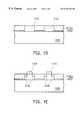
- FIGS. 1A through 1Eare schematic, cross-sectional views showing the processing steps for forming a MOSFET according to the preferred embodiment of this invention.
- FIGS. 1A through 1Eare schematic, cross-sectional views showing the processing steps for forming a MOSFET according to the preferred embodiment of this invention.
- a pad oxide layer 102 and a mask layer 104are formed on a substrate 100 in sequence.
- a patterned photoresist layer(not shown) is formed on the mask layer 104 to pattern the pad oxide layer 102 and the mask layer 104 , and then an opening 106 is formed in the pad oxide layer 102 and the mask layer 104 to expose the substrate 100 .
- the pad oxide layer 102is formed, for example, by thermal oxidation.
- the mask layer 104is, for example, a silicon nitride layer formed by, for example, chemical vapor deposition (CVD). The sum of the thickness of the pad oxide layer 102 and the thickness of the mask layer 104 is about 3000-4000 ⁇ .
- the opening 106is filled with an epitaxial silicon layer 110 .
- the method of forming the epitaxial silicon layer 110is described as follows. First, an epitaxial silicon layer (not shown) is deposited on the mask layer 104 and fills the opening 106 . Then, while the mask layer 104 serves as a stop layer, a portion of the epitaxial silicon layer is removed by etching back to form the epitaxial silicon layer 110 .
- a surface level of the epitaxial silicon layer 110is substantially the same as that of the mask layer 104 . Namely, the thickness of the epitaxial silicon layer 110 is about 3000-4000 ⁇ .
- the mask layer 104is removed to expose the pad oxide layer 102 , and then an oxide layer 112 is formed over the substrate 100 .
- the oxide layer 112 over the epitaxial silicon layer 110is removed by, for example, etching back or chemical mechanical polishing (CMP) to form an oxide layer 112 a .
- a surface level of the oxide layer 112 ais substantially the same as that of the epitaxial silicon layer 110 .
- the combination of the oxide layer 112 a next to the epitaxial silicon layer 110 and the pad oxide layer 102serves as a device isolation structure in the invention instead of the conventional device isolation structure.
- a gate 114is formed on the epitaxial silicon layer 110 by conventional technology, and then source/drain regions 116 are formed in the epitaxial silicon layer 110 .
- the inventionprovides a method for forming a device isolation structure without etching the substrate, so that stress and dislocation generation while etching the substrate can be avoided. As a result, leakage current is avoided.
- the feature of this inventionis that an epitaxial silicon layer with device isolation structures is formed over the substrate, wherein each device isolation structure is made of oxide.
- the inventionneed not etch the substrate to form a device isolation structure.
- the inventionnot only prevents stress and dislocation and avoids leakage current, but also provides an easiy method for forming a device isolation structure.
Landscapes
- Insulated Gate Type Field-Effect Transistor (AREA)
- Element Separation (AREA)
Abstract
Description
Claims (14)
Priority Applications (2)
| Application Number | Priority Date | Filing Date | Title |
|---|---|---|---|
| TW088112975ATW426940B (en) | 1999-07-30 | 1999-07-30 | Manufacturing method of MOS field effect transistor |
| US09/372,430US6274444B1 (en) | 1999-07-30 | 1999-08-10 | Method for forming mosfet |
Applications Claiming Priority (2)
| Application Number | Priority Date | Filing Date | Title |
|---|---|---|---|
| TW088112975ATW426940B (en) | 1999-07-30 | 1999-07-30 | Manufacturing method of MOS field effect transistor |
| US09/372,430US6274444B1 (en) | 1999-07-30 | 1999-08-10 | Method for forming mosfet |
Publications (1)
| Publication Number | Publication Date |
|---|---|
| US6274444B1true US6274444B1 (en) | 2001-08-14 |
Family
ID=26666721
Family Applications (1)
| Application Number | Title | Priority Date | Filing Date |
|---|---|---|---|
| US09/372,430Expired - Fee RelatedUS6274444B1 (en) | 1999-07-30 | 1999-08-10 | Method for forming mosfet |
Country Status (2)
| Country | Link |
|---|---|
| US (1) | US6274444B1 (en) |
| TW (1) | TW426940B (en) |
Cited By (74)
| Publication number | Priority date | Publication date | Assignee | Title |
|---|---|---|---|---|
| US20040238914A1 (en)* | 2003-05-30 | 2004-12-02 | International Business Machines Corporation | STI stress modification by nitrogen plasma treatment for improving performance in small width devices |
| US20040256700A1 (en)* | 2003-06-17 | 2004-12-23 | International Business Machines Corporation | High-performance CMOS devices on hybrid crystal oriented substrates |
| US20040262784A1 (en)* | 2003-06-30 | 2004-12-30 | International Business Machines Corporation | High performance cmos device structures and method of manufacture |
| US20050054148A1 (en)* | 2003-09-10 | 2005-03-10 | International Business Machines Corporation | METHOD AND STRUCTURE FOR IMPROVED MOSFETs USING POLY/SILICIDE GATE HEIGHT CONTROL |
| US20050054145A1 (en)* | 2003-09-09 | 2005-03-10 | International Business Machines Corporation | Method for reduced n+ diffusion in strained si on sige substrate |
| US20050059214A1 (en)* | 2003-09-16 | 2005-03-17 | International Business Machines Corporation | Method and structure of vertical strained silicon devices |
| US6869866B1 (en) | 2003-09-22 | 2005-03-22 | International Business Machines Corporation | Silicide proximity structures for CMOS device performance improvements |
| US20050064646A1 (en)* | 2003-09-23 | 2005-03-24 | Dureseti Chidambarrao | NFETs using gate induced stress modulation |
| US20050064686A1 (en)* | 2003-09-23 | 2005-03-24 | Dureseti Chidambarrao | Strained silicon on relaxed sige film with uniform misfit dislocation density |
| US20050085022A1 (en)* | 2003-10-20 | 2005-04-21 | Dureseti Chidambarrao | Strained dislocation-free channels for CMOS and method of manufacture |
| US20050082616A1 (en)* | 2003-10-20 | 2005-04-21 | Huajie Chen | High performance stress-enhanced MOSFETs using Si:C and SiGe epitaxial source/drain and method of manufacture |
| US6887751B2 (en) | 2003-09-12 | 2005-05-03 | International Business Machines Corporation | MOSFET performance improvement using deformation in SOI structure |
| US20050093076A1 (en)* | 2003-11-05 | 2005-05-05 | International Business Machines Corporation | METHOD AND STRUCTURE FOR FORMING STRAINED Si FOR CMOS DEVICES |
| US20050098829A1 (en)* | 2003-11-06 | 2005-05-12 | Doris Bruce B. | High mobility CMOS circuits |
| US20050106790A1 (en)* | 2003-11-13 | 2005-05-19 | Kangguo Cheng | Strained silicon on a SiGe on SOI substrate |
| US20050106799A1 (en)* | 2003-11-14 | 2005-05-19 | International Business Machines Corporation | Stressed semiconductor device structures having granular semiconductor material |
| US20050104131A1 (en)* | 2003-11-19 | 2005-05-19 | Dureseti Chidambarrao | Silicon device on Si:C-OI and SGOI and method of manufacture |
| US20050130358A1 (en)* | 2003-12-12 | 2005-06-16 | Dureseti Chidambarrao | Strained finFETs and method of manufacture |
| US20050136584A1 (en)* | 2003-12-23 | 2005-06-23 | Boyan Boyanov | Strained transistor integration for CMOS |
| US20050145954A1 (en)* | 2004-01-05 | 2005-07-07 | International Business Machines Corporation | Structures and methods for making strained mosfets |
| US20050158955A1 (en)* | 2004-01-16 | 2005-07-21 | International Business Machines Corporation | Method and apparatus to increase strain effect in a transistor channel |
| US20050189589A1 (en)* | 2004-02-27 | 2005-09-01 | International Business Machines Corporation | Hybrid soi/bulk semiconductor transistors |
| US20050194699A1 (en)* | 2004-03-03 | 2005-09-08 | International Business Machines Corporation | Mobility enhanced cmos devices |
| US20050236668A1 (en)* | 2004-04-23 | 2005-10-27 | International Business Machines Corporation | STRUCTURES AND METHODS FOR MANUFACTURING OF DISLOCATION FREE STRESSED CHANNELS IN BULK SILICON AND SOI CMOS DEVICES BY GATE STRESS ENGINEERING WITH SiGe AND/OR Si:C |
| US20050269561A1 (en)* | 2004-06-03 | 2005-12-08 | Dureseti Chidambarrao | Strained Si on multiple materials for bulk or SOI substrates |
| US20050277271A1 (en)* | 2004-06-09 | 2005-12-15 | International Business Machines Corporation | RAISED STI PROCESS FOR MULTIPLE GATE OX AND SIDEWALL PROTECTION ON STRAINED Si/SGOI STRUCTURE WITH ELEVATED SOURCE/DRAIN |
| US20050285192A1 (en)* | 2004-06-29 | 2005-12-29 | International Business Machines Corporation | Structures and methods for manufacturing p-type mosfet withgraded embedded silicon-germanium source-drain and/or extension |
| US20050285187A1 (en)* | 2004-06-24 | 2005-12-29 | International Business Machines Corporation | Strained-silicon CMOS device and method |
| US20060001089A1 (en)* | 2004-07-02 | 2006-01-05 | International Business Machines Corporation | Ultra-thin, high quality strained silicon-on-insulator formed by elastic strain transfer |
| US20060019462A1 (en)* | 2004-07-23 | 2006-01-26 | International Business Machines Corporation | Patterned strained semiconductor substrate and device |
| US20060057787A1 (en)* | 2002-11-25 | 2006-03-16 | Doris Bruce B | Strained finfet cmos device structures |
| US20060113568A1 (en)* | 2004-11-30 | 2006-06-01 | International Business Machines Corporation | Structure and method of applying stresses to pfet and nfet transistor channels for improved performance |
| US20060118912A1 (en)* | 2004-12-08 | 2006-06-08 | International Business Machines Corporation | Methodology for recovery of hot carrier induced degradation in bipolar devices |
| US20060125008A1 (en)* | 2004-12-14 | 2006-06-15 | International Business Machines Corporation | Dual stressed soi substrates |
| US20060151838A1 (en)* | 2005-01-12 | 2006-07-13 | International Business Machines Corporation | Enhanced pfet using shear stress |
| US20060160317A1 (en)* | 2005-01-18 | 2006-07-20 | International Business Machines Corporation | Structure and method to enhance stress in a channel of cmos devices using a thin gate |
| US20060157795A1 (en)* | 2005-01-19 | 2006-07-20 | International Business Machines Corporation | Structure and method to optimize strain in cmosfets |
| US20060172500A1 (en)* | 2005-02-01 | 2006-08-03 | International Business Machines Corporation | Stucture and method to induce strain in a semiconductor device channel with stressed film under the gate |
| US20060172495A1 (en)* | 2005-01-28 | 2006-08-03 | International Business Machines Corporation | STRUCTURE AND METHOD FOR MANUFACTURING PLANAR STRAINED Si/SiGe SUBSTRATE WITH MULTIPLE ORIENTATIONS AND DIFFERENT STRESS LEVELS |
| US20060180866A1 (en)* | 2005-02-15 | 2006-08-17 | International Business Machines Corporation | Structure and method for manufacturing strained finfet |
| US7119403B2 (en) | 2003-10-16 | 2006-10-10 | International Business Machines Corporation | High performance strained CMOS devices |
| US20060228836A1 (en)* | 2005-04-12 | 2006-10-12 | International Business Machines Corporation | Method and structure for forming strained devices |
| US20070045775A1 (en)* | 2005-08-26 | 2007-03-01 | Adam Thomas N | Mobility enhancement in SiGe heterojunction bipolar transistors |
| US20070069294A1 (en)* | 2005-09-29 | 2007-03-29 | International Business Machines Corporation | Stress engineering using dual pad nitride with selective soi device architecture |
| US7202132B2 (en) | 2004-01-16 | 2007-04-10 | International Business Machines Corporation | Protecting silicon germanium sidewall with silicon for strained silicon/silicon germanium MOSFETs |
| US20070096206A1 (en)* | 2005-11-03 | 2007-05-03 | International Business Machines Corporation | Gate electrode stress control for finfet performance enhancement |
| US20070099360A1 (en)* | 2005-11-03 | 2007-05-03 | International Business Machines Corporation | Integrated circuits having strained channel field effect transistors and methods of making |
| US20070096170A1 (en)* | 2005-11-02 | 2007-05-03 | International Business Machines Corporation | Low modulus spacers for channel stress enhancement |
| US20070105299A1 (en)* | 2005-11-10 | 2007-05-10 | International Business Machines Corporation | Dual stress memory technique method and related structure |
| US7217949B2 (en) | 2004-07-01 | 2007-05-15 | International Business Machines Corporation | Strained Si MOSFET on tensile-strained SiGe-on-insulator (SGOI) |
| US20070108531A1 (en)* | 2005-11-14 | 2007-05-17 | International Business Machines Corporation | Rotational shear stress for charge carrier mobility modification |
| US20070108525A1 (en)* | 2005-11-14 | 2007-05-17 | International Business Machines Corporation | Structure and method to increase strain enhancement with spacerless fet and dual liner process |
| US20070111417A1 (en)* | 2004-08-31 | 2007-05-17 | International Business Machines Corporation | Strained-silicon cmos device and method |
| US20070120154A1 (en)* | 2005-11-30 | 2007-05-31 | International Business Machines Corporation | Finfet structure with multiply stressed gate electrode |
| US20070158753A1 (en)* | 2006-01-09 | 2007-07-12 | International Business Machines Corporation | Semiconductor device structure having low and high performance devices of same conductive type on same substrate |
| US20070158743A1 (en)* | 2006-01-11 | 2007-07-12 | International Business Machines Corporation | Thin silicon single diffusion field effect transistor for enhanced drive performance with stress film liners |
| US20070196987A1 (en)* | 2006-02-21 | 2007-08-23 | Dureseti Chidambarrao | Pseudomorphic Si/SiGe/Si body device with embedded SiGe source/drain |
| US20070202654A1 (en)* | 2006-02-28 | 2007-08-30 | International Business Machines Corporation | Spacer and process to enhance the strain in the channel with stress liner |
| US20070252214A1 (en)* | 2006-04-28 | 2007-11-01 | International Business Machines Corporation | Cmos structures and methods using self-aligned dual stressed layers |
| US20070254423A1 (en)* | 2006-04-28 | 2007-11-01 | International Business Machines Corporation | High performance stress-enhance mosfet and method of manufacture |
| US20070254422A1 (en)* | 2006-04-28 | 2007-11-01 | International Business Machines Corporation | High performance stress-enhance mosfet and method of manufacture |
| US7314789B2 (en) | 2004-12-15 | 2008-01-01 | International Business Machines Corporation | Structure and method to generate local mechanical gate stress for MOSFET channel mobility modification |
| US20080001182A1 (en)* | 2006-06-29 | 2008-01-03 | International Business Machines Corporation | Improved cmos devices with stressed channel regions, and methods for fabricating the same |
| US20080057673A1 (en)* | 2006-08-30 | 2008-03-06 | International Business Machines Corporation | Semiconductor structure and method of making same |
| US20080057653A1 (en)* | 2006-08-30 | 2008-03-06 | International Business Machines Corporation | Method and structure for improving device performance variation in dual stress liner technology |
| US7381609B2 (en) | 2004-01-16 | 2008-06-03 | International Business Machines Corporation | Method and structure for controlling stress in a transistor channel |
| US20080217665A1 (en)* | 2006-01-10 | 2008-09-11 | International Business Machines Corporation | Semiconductor device structure having enhanced performance fet device |
| US20080258180A1 (en)* | 2006-01-09 | 2008-10-23 | International Business Machines Corporation | Cross-section hourglass shaped channel region for charge carrier mobility modification |
| US20090127626A1 (en)* | 2007-11-15 | 2009-05-21 | International Business Machines Corporation | Stress-generating shallow trench isolation structure having dual composition |
| US7790540B2 (en) | 2006-08-25 | 2010-09-07 | International Business Machines Corporation | Structure and method to use low k stress liner to reduce parasitic capacitance |
| US20110140242A1 (en)* | 2009-12-16 | 2011-06-16 | National Semiconductor Corporation | Stress compensation for large area gallium nitride or other nitride-based structures on semiconductor substrates |
| US20110230030A1 (en)* | 2010-03-16 | 2011-09-22 | International Business Machines Corporation | Strain-preserving ion implantation methods |
| US8115254B2 (en) | 2007-09-25 | 2012-02-14 | International Business Machines Corporation | Semiconductor-on-insulator structures including a trench containing an insulator stressor plug and method of fabricating same |
| US9659960B1 (en) | 2015-12-09 | 2017-05-23 | International Business Machines Corporation | Extremely thin silicon-on-insulator silicon germanium device without edge strain relaxation |
Citations (1)
| Publication number | Priority date | Publication date | Assignee | Title |
|---|---|---|---|---|
| US5959331A (en)* | 1997-05-03 | 1999-09-28 | United Micorelectronics Corp. | High density transistor component and its manufacturing method |
- 1999
- 1999-07-30TWTW088112975Apatent/TW426940B/ennot_activeIP Right Cessation
- 1999-08-10USUS09/372,430patent/US6274444B1/ennot_activeExpired - Fee Related
Patent Citations (2)
| Publication number | Priority date | Publication date | Assignee | Title |
|---|---|---|---|---|
| US5959331A (en)* | 1997-05-03 | 1999-09-28 | United Micorelectronics Corp. | High density transistor component and its manufacturing method |
| US6010928A (en)* | 1997-05-03 | 2000-01-04 | United Microelectronics Corp. | High density transistor component and its manufacturing method |
Cited By (257)
| Publication number | Priority date | Publication date | Assignee | Title |
|---|---|---|---|---|
| US7388259B2 (en) | 2002-11-25 | 2008-06-17 | International Business Machines Corporation | Strained finFET CMOS device structures |
| US20060057787A1 (en)* | 2002-11-25 | 2006-03-16 | Doris Bruce B | Strained finfet cmos device structures |
| US20040238914A1 (en)* | 2003-05-30 | 2004-12-02 | International Business Machines Corporation | STI stress modification by nitrogen plasma treatment for improving performance in small width devices |
| US7479688B2 (en) | 2003-05-30 | 2009-01-20 | International Business Machines Corporation | STI stress modification by nitrogen plasma treatment for improving performance in small width devices |
| US7713807B2 (en) | 2003-06-17 | 2010-05-11 | International Business Machines Corporation | High-performance CMOS SOI devices on hybrid crystal-oriented substrates |
| US20080096330A1 (en)* | 2003-06-17 | 2008-04-24 | International Business Machines Corporation | High-performance cmos soi devices on hybrid crystal-oriented substrates |
| US20040256700A1 (en)* | 2003-06-17 | 2004-12-23 | International Business Machines Corporation | High-performance CMOS devices on hybrid crystal oriented substrates |
| US7329923B2 (en) | 2003-06-17 | 2008-02-12 | International Business Machines Corporation | High-performance CMOS devices on hybrid crystal oriented substrates |
| US7436029B2 (en) | 2003-06-30 | 2008-10-14 | International Business Machines Corporation | High performance CMOS device structures and method of manufacture |
| US20040262784A1 (en)* | 2003-06-30 | 2004-12-30 | International Business Machines Corporation | High performance cmos device structures and method of manufacture |
| US20080026522A1 (en)* | 2003-06-30 | 2008-01-31 | International Business Machines Corporation | High performance cmos device structures and method of manufacture |
| US7279746B2 (en) | 2003-06-30 | 2007-10-09 | International Business Machines Corporation | High performance CMOS device structures and method of manufacture |
| US20050054145A1 (en)* | 2003-09-09 | 2005-03-10 | International Business Machines Corporation | Method for reduced n+ diffusion in strained si on sige substrate |
| US7297601B2 (en) | 2003-09-09 | 2007-11-20 | International Business Machines Corporation | Method for reduced N+ diffusion in strained Si on SiGe substrate |
| US7345329B2 (en) | 2003-09-09 | 2008-03-18 | International Business Machines Corporation | Method for reduced N+ diffusion in strained Si on SiGe substrate |
| US20050145992A1 (en)* | 2003-09-09 | 2005-07-07 | Dureseti Chidambarrao | Method for reduced N+ diffusion in strained Si on SiGe substrate |
| US7410846B2 (en) | 2003-09-09 | 2008-08-12 | International Business Machines Corporation | Method for reduced N+ diffusion in strained Si on SiGe substrate |
| US7091563B2 (en) | 2003-09-10 | 2006-08-15 | International Business Machines Corporation | Method and structure for improved MOSFETs using poly/silicide gate height control |
| US6890808B2 (en) | 2003-09-10 | 2005-05-10 | International Business Machines Corporation | Method and structure for improved MOSFETs using poly/silicide gate height control |
| US20050054148A1 (en)* | 2003-09-10 | 2005-03-10 | International Business Machines Corporation | METHOD AND STRUCTURE FOR IMPROVED MOSFETs USING POLY/SILICIDE GATE HEIGHT CONTROL |
| US20050145950A1 (en)* | 2003-09-10 | 2005-07-07 | Dureseti Chidambarrao | Method and structure for improved MOSFETs using poly/silicide gate height control |
| US7745277B2 (en) | 2003-09-12 | 2010-06-29 | International Business Machines Corporation | MOSFET performance improvement using deformation in SOI structure |
| US6887751B2 (en) | 2003-09-12 | 2005-05-03 | International Business Machines Corporation | MOSFET performance improvement using deformation in SOI structure |
| US20050142788A1 (en)* | 2003-09-12 | 2005-06-30 | Dureseti Chidambarrao | MOSFET performance improvement using deformation in SOI structure |
| US7170126B2 (en) | 2003-09-16 | 2007-01-30 | International Business Machines Corporation | Structure of vertical strained silicon devices |
| US20050059214A1 (en)* | 2003-09-16 | 2005-03-17 | International Business Machines Corporation | Method and structure of vertical strained silicon devices |
| US20050064687A1 (en)* | 2003-09-22 | 2005-03-24 | International Business Machines Corporation | Silicide proximity structures for cmos device performance improvements |
| US6869866B1 (en) | 2003-09-22 | 2005-03-22 | International Business Machines Corporation | Silicide proximity structures for CMOS device performance improvements |
| US7964865B2 (en) | 2003-09-23 | 2011-06-21 | International Business Machines Corporation | Strained silicon on relaxed sige film with uniform misfit dislocation density |
| US20050164477A1 (en)* | 2003-09-23 | 2005-07-28 | Dureseti Chidambarrao | Strained silicon on relaxed sige film with uniform misfit dislocation density |
| US7144767B2 (en) | 2003-09-23 | 2006-12-05 | International Business Machines Corporation | NFETs using gate induced stress modulation |
| US6872641B1 (en) | 2003-09-23 | 2005-03-29 | International Business Machines Corporation | Strained silicon on relaxed sige film with uniform misfit dislocation density |
| US20060145274A1 (en)* | 2003-09-23 | 2006-07-06 | International Business Machines Corporation | NFETs using gate induced stress modulation |
| US20050064686A1 (en)* | 2003-09-23 | 2005-03-24 | Dureseti Chidambarrao | Strained silicon on relaxed sige film with uniform misfit dislocation density |
| US20050064646A1 (en)* | 2003-09-23 | 2005-03-24 | Dureseti Chidambarrao | NFETs using gate induced stress modulation |
| US7119403B2 (en) | 2003-10-16 | 2006-10-10 | International Business Machines Corporation | High performance strained CMOS devices |
| US20060270136A1 (en)* | 2003-10-16 | 2006-11-30 | International Business Machines Corporation | High performance strained cmos devices |
| US7847358B2 (en) | 2003-10-16 | 2010-12-07 | International Business Machines Corporation | High performance strained CMOS devices |
| US7037770B2 (en) | 2003-10-20 | 2006-05-02 | International Business Machines Corporation | Method of manufacturing strained dislocation-free channels for CMOS |
| US20070296038A1 (en)* | 2003-10-20 | 2007-12-27 | International Business Machines Corporation | High performance stress-enhanced mosfets using si:c and sige epitaxial source/drain and method of manufacture |
| US7495291B2 (en) | 2003-10-20 | 2009-02-24 | International Business Machines Corporation | Strained dislocation-free channels for CMOS and method of manufacture |
| US20050085022A1 (en)* | 2003-10-20 | 2005-04-21 | Dureseti Chidambarrao | Strained dislocation-free channels for CMOS and method of manufacture |
| US20050082616A1 (en)* | 2003-10-20 | 2005-04-21 | Huajie Chen | High performance stress-enhanced MOSFETs using Si:C and SiGe epitaxial source/drain and method of manufacture |
| US20050139930A1 (en)* | 2003-10-20 | 2005-06-30 | Dureseti Chidambarrao | Strained dislocation-free channels for CMOS and method of manufacture |
| US9023698B2 (en) | 2003-10-20 | 2015-05-05 | Samsung Electronics Co., Ltd. | High performance stress-enhanced MOSFETs using Si:C and SiGe epitaxial source/drain and method of manufacture |
| US20070264783A1 (en)* | 2003-10-20 | 2007-11-15 | International Business Machines Corporation | High performance stress-enhanced mosfets using si:c and sige epitaxial source/drain and method of manufacture |
| US9401424B2 (en) | 2003-10-20 | 2016-07-26 | Samsung Electronics Co., Ltd. | High performance stress-enhanced MOSFETs using Si:C and SiGe epitaxial source/drain and method of manufacture |
| US8901566B2 (en) | 2003-10-20 | 2014-12-02 | International Business Machines Corporation | High performance stress-enhanced MOSFETs using Si:C and SiGe epitaxial source/drain and method of manufacture |
| US8168489B2 (en) | 2003-10-20 | 2012-05-01 | International Business Machines Corporation | High performance stress-enhanced MOSFETS using Si:C and SiGe epitaxial source/drain and method of manufacture |
| US7303949B2 (en) | 2003-10-20 | 2007-12-04 | International Business Machines Corporation | High performance stress-enhanced MOSFETs using Si:C and SiGe epitaxial source/drain and method of manufacture |
| US7129126B2 (en) | 2003-11-05 | 2006-10-31 | International Business Machines Corporation | Method and structure for forming strained Si for CMOS devices |
| US20050093076A1 (en)* | 2003-11-05 | 2005-05-05 | International Business Machines Corporation | METHOD AND STRUCTURE FOR FORMING STRAINED Si FOR CMOS DEVICES |
| US20080003735A1 (en)* | 2003-11-05 | 2008-01-03 | International Business Machines Corporation | Method and structure for forming strained si for cmos devices |
| US7550338B2 (en) | 2003-11-05 | 2009-06-23 | International Business Machines Corporation | Method and structure for forming strained SI for CMOS devices |
| US20070020806A1 (en)* | 2003-11-05 | 2007-01-25 | International Business Machines Corporation | Method and structure for forming strained si for cmos devices |
| US7700951B2 (en) | 2003-11-05 | 2010-04-20 | International Business Machines Corporation | Method and structure for forming strained Si for CMOS devices |
| US20100109048A1 (en)* | 2003-11-05 | 2010-05-06 | International Business Machines Corporation | Method and structure for forming strained si for cmos devices |
| US7429752B2 (en) | 2003-11-05 | 2008-09-30 | International Business Machines Corporation | Method and structure for forming strained SI for CMOS devices |
| US20080283824A1 (en)* | 2003-11-05 | 2008-11-20 | International Business Machines Corporation, | Method and structure for forming strained si for cmos devices |
| US7928443B2 (en) | 2003-11-05 | 2011-04-19 | International Business Machines Corporation | Method and structure for forming strained SI for CMOS devices |
| US20060027868A1 (en)* | 2003-11-06 | 2006-02-09 | Ibm Corporation | High mobility CMOS circuits |
| US20050098829A1 (en)* | 2003-11-06 | 2005-05-12 | Doris Bruce B. | High mobility CMOS circuits |
| US7015082B2 (en) | 2003-11-06 | 2006-03-21 | International Business Machines Corporation | High mobility CMOS circuits |
| US7285826B2 (en) | 2003-11-06 | 2007-10-23 | International Business Machines Corporation | High mobility CMOS circuits |
| US20080237720A1 (en)* | 2003-11-06 | 2008-10-02 | International Business Machines Corporation | High mobility cmos circuits |
| US8013392B2 (en) | 2003-11-06 | 2011-09-06 | International Business Machines Corporation | High mobility CMOS circuits |
| US20050142700A1 (en)* | 2003-11-13 | 2005-06-30 | Kangguo Cheng | Strained silicon on a SiGe on SOI substrate |
| US7468538B2 (en) | 2003-11-13 | 2008-12-23 | International Business Machines Corporation | Strained silicon on a SiGe on SOI substrate |
| US7029964B2 (en) | 2003-11-13 | 2006-04-18 | International Business Machines Corporation | Method of manufacturing a strained silicon on a SiGe on SOI substrate |
| CN100362618C (en)* | 2003-11-13 | 2008-01-16 | 国际商业机器公司 | A kind of semiconductor device and manufacturing method |
| US20050106790A1 (en)* | 2003-11-13 | 2005-05-19 | Kangguo Cheng | Strained silicon on a SiGe on SOI substrate |
| US7122849B2 (en) | 2003-11-14 | 2006-10-17 | International Business Machines Corporation | Stressed semiconductor device structures having granular semiconductor material |
| US20080064172A1 (en)* | 2003-11-14 | 2008-03-13 | International Business Machines Corporation | Stressed semiconductor device structures having granular semiconductor material |
| US20050106799A1 (en)* | 2003-11-14 | 2005-05-19 | International Business Machines Corporation | Stressed semiconductor device structures having granular semiconductor material |
| US7488658B2 (en) | 2003-11-14 | 2009-02-10 | International Business Machines Corporation | Stressed semiconductor device structures having granular semiconductor material |
| US8232153B2 (en) | 2003-11-19 | 2012-07-31 | International Business Machines Corporation | Silicon device on Si:C-OI and SGOI and method of manufacture |
| US8633071B2 (en) | 2003-11-19 | 2014-01-21 | International Business Machines Corporation | Silicon device on Si: C-oi and Sgoi and method of manufacture |
| US20070228472A1 (en)* | 2003-11-19 | 2007-10-04 | International Business Machines Corporation | Silicon device on si: c-oi and sgoi and method of manufacture |
| US9040373B2 (en) | 2003-11-19 | 2015-05-26 | International Business Machines Corporation | Silicon device on SI:C-OI and SGOI and method of manufacture |
| US20050104131A1 (en)* | 2003-11-19 | 2005-05-19 | Dureseti Chidambarrao | Silicon device on Si:C-OI and SGOI and method of manufacture |
| US7247534B2 (en) | 2003-11-19 | 2007-07-24 | International Business Machines Corporation | Silicon device on Si:C-OI and SGOI and method of manufacture |
| US8119472B2 (en) | 2003-11-19 | 2012-02-21 | International Business Machines Corporation | Silicon device on Si:C SOI and SiGe and method of manufacture |
| US7198995B2 (en) | 2003-12-12 | 2007-04-03 | International Business Machines Corporation | Strained finFETs and method of manufacture |
| US20050130358A1 (en)* | 2003-12-12 | 2005-06-16 | Dureseti Chidambarrao | Strained finFETs and method of manufacture |
| US8748869B2 (en) | 2003-12-23 | 2014-06-10 | Intel Corporation | Strained transistor integration for CMOS |
| US20100044754A1 (en)* | 2003-12-23 | 2010-02-25 | Boyan Boyanov | Strained transistor integration for cmos |
| US7662689B2 (en)* | 2003-12-23 | 2010-02-16 | Intel Corporation | Strained transistor integration for CMOS |
| US9112029B2 (en) | 2003-12-23 | 2015-08-18 | Intel Corporation | Strained transistor integration for CMOS |
| US8373154B2 (en) | 2003-12-23 | 2013-02-12 | Intel Corporation | Strained transistor integration for CMOS |
| US20050136584A1 (en)* | 2003-12-23 | 2005-06-23 | Boyan Boyanov | Strained transistor integration for CMOS |
| US20050145954A1 (en)* | 2004-01-05 | 2005-07-07 | International Business Machines Corporation | Structures and methods for making strained mosfets |
| US20070218620A1 (en)* | 2004-01-05 | 2007-09-20 | International Business Machines Corporation | Structures and methods for making strained mosfets |
| US7749842B2 (en) | 2004-01-05 | 2010-07-06 | International Business Machines Corporation | Structures and methods for making strained MOSFETs |
| US7247912B2 (en) | 2004-01-05 | 2007-07-24 | International Business Machines Corporation | Structures and methods for making strained MOSFETs |
| US7498602B2 (en) | 2004-01-16 | 2009-03-03 | International Business Machines Corporation | Protecting silicon germanium sidewall with silicon for strained silicon/silicon mosfets |
| US7462915B2 (en) | 2004-01-16 | 2008-12-09 | International Business Machines Corporation | Method and apparatus for increase strain effect in a transistor channel |
| US7118999B2 (en) | 2004-01-16 | 2006-10-10 | International Business Machines Corporation | Method and apparatus to increase strain effect in a transistor channel |
| US20060281272A1 (en)* | 2004-01-16 | 2006-12-14 | International Business Machines Corporation | Method and apparatus for increase strain effect in a transistor channel |
| US20050158955A1 (en)* | 2004-01-16 | 2005-07-21 | International Business Machines Corporation | Method and apparatus to increase strain effect in a transistor channel |
| US7202132B2 (en) | 2004-01-16 | 2007-04-10 | International Business Machines Corporation | Protecting silicon germanium sidewall with silicon for strained silicon/silicon germanium MOSFETs |
| US7790558B2 (en) | 2004-01-16 | 2010-09-07 | International Business Machines Corporation | Method and apparatus for increase strain effect in a transistor channel |
| US7381609B2 (en) | 2004-01-16 | 2008-06-03 | International Business Machines Corporation | Method and structure for controlling stress in a transistor channel |
| US7452761B2 (en) | 2004-02-27 | 2008-11-18 | International Business Machines Corporation | Hybrid SOI-bulk semiconductor transistors |
| US7923782B2 (en) | 2004-02-27 | 2011-04-12 | International Business Machines Corporation | Hybrid SOI/bulk semiconductor transistors |
| US20080090366A1 (en)* | 2004-02-27 | 2008-04-17 | Huilong Zhu | Hybrid SOI-Bulk Semiconductor Transistors |
| US20050189589A1 (en)* | 2004-02-27 | 2005-09-01 | International Business Machines Corporation | Hybrid soi/bulk semiconductor transistors |
| US7767503B2 (en) | 2004-02-27 | 2010-08-03 | International Business Machines Corporation | Hybrid SOI/bulk semiconductor transistors |
| US20060148147A1 (en)* | 2004-03-03 | 2006-07-06 | Ibm | Mobility enhanced CMOS devices |
| US20050194699A1 (en)* | 2004-03-03 | 2005-09-08 | International Business Machines Corporation | Mobility enhanced cmos devices |
| US7205206B2 (en) | 2004-03-03 | 2007-04-17 | International Business Machines Corporation | Method of fabricating mobility enhanced CMOS devices |
| US7569848B2 (en) | 2004-03-03 | 2009-08-04 | International Business Machines Corporation | Mobility enhanced CMOS devices |
| US20050236668A1 (en)* | 2004-04-23 | 2005-10-27 | International Business Machines Corporation | STRUCTURES AND METHODS FOR MANUFACTURING OF DISLOCATION FREE STRESSED CHANNELS IN BULK SILICON AND SOI CMOS DEVICES BY GATE STRESS ENGINEERING WITH SiGe AND/OR Si:C |
| US20090149010A1 (en)* | 2004-04-23 | 2009-06-11 | International Business Machines Corporation | STRUCTURES AND METHODS FOR MANUFACTURING OF DISLOCATION FREE STRESSED CHANNELS IN BULK SILICON AND SOI MOS DEVICES BY GATE STRESS ENGINEERING WITH SiGe AND/OR Si:C |
| US7713806B2 (en) | 2004-04-23 | 2010-05-11 | International Business Machines Corporation | Structures and methods for manufacturing of dislocation free stressed channels in bulk silicon and SOI MOS devices by gate stress engineering with SiGe and/or Si:C |
| US7476580B2 (en) | 2004-04-23 | 2009-01-13 | International Business Machines Corporation | Structures and methods for manufacturing of dislocation free stressed channels in bulk silicon and SOI CMOS devices by gate stress engineering with SiGe and/or Si:C |
| US7504693B2 (en) | 2004-04-23 | 2009-03-17 | International Business Machines Corporation | Dislocation free stressed channels in bulk silicon and SOI CMOS devices by gate stress engineering |
| US7560328B2 (en) | 2004-06-03 | 2009-07-14 | International Business Machines Corporation | Strained Si on multiple materials for bulk or SOI substrates |
| US20050269561A1 (en)* | 2004-06-03 | 2005-12-08 | Dureseti Chidambarrao | Strained Si on multiple materials for bulk or SOI substrates |
| US7223994B2 (en) | 2004-06-03 | 2007-05-29 | International Business Machines Corporation | Strained Si on multiple materials for bulk or SOI substrates |
| US20070166897A1 (en)* | 2004-06-03 | 2007-07-19 | International Business Machines Corporation | STRAINED Si ON MULTIPLE MATERIALS FOR BULK OR SOI SUBSTRATES |
| US7037794B2 (en) | 2004-06-09 | 2006-05-02 | International Business Machines Corporation | Raised STI process for multiple gate ox and sidewall protection on strained Si/SGOI structure with elevated source/drain |
| US20060128111A1 (en)* | 2004-06-09 | 2006-06-15 | International Business Machines Corporation | Raised sti process for multiple gate ox and sidewall protection on strained Si/SGOI structure with elevated source/drain |
| US20050277271A1 (en)* | 2004-06-09 | 2005-12-15 | International Business Machines Corporation | RAISED STI PROCESS FOR MULTIPLE GATE OX AND SIDEWALL PROTECTION ON STRAINED Si/SGOI STRUCTURE WITH ELEVATED SOURCE/DRAIN |
| US7737502B2 (en) | 2004-06-09 | 2010-06-15 | International Business Machines Corporation | Raised STI process for multiple gate ox and sidewall protection on strained Si/SGOI sructure with elevated source/drain |
| US20050285187A1 (en)* | 2004-06-24 | 2005-12-29 | International Business Machines Corporation | Strained-silicon CMOS device and method |
| US20100244139A1 (en)* | 2004-06-24 | 2010-09-30 | International Business Machines Corporation | Strained-silicon cmos device and method |
| US20090305474A1 (en)* | 2004-06-24 | 2009-12-10 | International Business Machines Corporation | Strained-silicon cmos device and method |
| US7227205B2 (en) | 2004-06-24 | 2007-06-05 | International Business Machines Corporation | Strained-silicon CMOS device and method |
| US20050285192A1 (en)* | 2004-06-29 | 2005-12-29 | International Business Machines Corporation | Structures and methods for manufacturing p-type mosfet withgraded embedded silicon-germanium source-drain and/or extension |
| US7288443B2 (en) | 2004-06-29 | 2007-10-30 | International Business Machines Corporation | Structures and methods for manufacturing p-type MOSFET with graded embedded silicon-germanium source-drain and/or extension |
| US20080042166A1 (en)* | 2004-07-01 | 2008-02-21 | International Business Machines Corporation | STRAINED Si MOSFET ON TENSILE-STRAINED SiGe-ON-INSULATOR (SGOI) |
| US7507989B2 (en) | 2004-07-01 | 2009-03-24 | International Business Machines Corporation | Strained Si MOSFET on tensile-strained SiGe-on-insulator (SGOI) |
| US8017499B2 (en) | 2004-07-01 | 2011-09-13 | International Business Machines Corporation | Strained Si MOSFET on tensile-strained SiGe-on-insulator (SGOI) |
| US20070155130A1 (en)* | 2004-07-01 | 2007-07-05 | International Business Machines Corporation | STRAINED Si MOSFET ON TENSILE-STRAINED SiGe-ON-INSULATOR (SGOI) |
| US7485518B2 (en) | 2004-07-01 | 2009-02-03 | International Business Machines Corporation | Strained Si MOSFET on tensile-strained SiGe-on-insulator (SGOI) |
| US7217949B2 (en) | 2004-07-01 | 2007-05-15 | International Business Machines Corporation | Strained Si MOSFET on tensile-strained SiGe-on-insulator (SGOI) |
| US20080220588A1 (en)* | 2004-07-01 | 2008-09-11 | International Business Machines Corporation | STRAINED Si MOSFET ON TENSILE-STRAINED SiGe-ON-INSULATOR (SGOI) |
| US6991998B2 (en) | 2004-07-02 | 2006-01-31 | International Business Machines Corporation | Ultra-thin, high quality strained silicon-on-insulator formed by elastic strain transfer |
| US7442993B2 (en) | 2004-07-02 | 2008-10-28 | International Business Machines Corporation | Ultra-thin, high quality strained silicon-on-insulator formed by elastic strain transfer |
| US20060001089A1 (en)* | 2004-07-02 | 2006-01-05 | International Business Machines Corporation | Ultra-thin, high quality strained silicon-on-insulator formed by elastic strain transfer |
| US20060081837A1 (en)* | 2004-07-02 | 2006-04-20 | International Business Machines Corporation | Ultra-thin, high quality strained silicon-on-insulator formed by elastic strain transfer |
| US20060019462A1 (en)* | 2004-07-23 | 2006-01-26 | International Business Machines Corporation | Patterned strained semiconductor substrate and device |
| US7682859B2 (en) | 2004-07-23 | 2010-03-23 | International Business Machines Corporation | Patterned strained semiconductor substrate and device |
| US9053970B2 (en) | 2004-07-23 | 2015-06-09 | International Business Machines Corporation | Patterned strained semiconductor substrate and device |
| US7384829B2 (en) | 2004-07-23 | 2008-06-10 | International Business Machines Corporation | Patterned strained semiconductor substrate and device |
| US9515140B2 (en) | 2004-07-23 | 2016-12-06 | Globalfoundries Inc. | Patterned strained semiconductor substrate and device |
| US20080061317A1 (en)* | 2004-07-23 | 2008-03-13 | International Business Machines Corporation | Patterned strained semiconductor substrate and device |
| US20070111417A1 (en)* | 2004-08-31 | 2007-05-17 | International Business Machines Corporation | Strained-silicon cmos device and method |
| US7808081B2 (en) | 2004-08-31 | 2010-10-05 | International Business Machines Corporation | Strained-silicon CMOS device and method |
| US20060113568A1 (en)* | 2004-11-30 | 2006-06-01 | International Business Machines Corporation | Structure and method of applying stresses to pfet and nfet transistor channels for improved performance |
| US7193254B2 (en) | 2004-11-30 | 2007-03-20 | International Business Machines Corporation | Structure and method of applying stresses to PFET and NFET transistor channels for improved performance |
| US20060118912A1 (en)* | 2004-12-08 | 2006-06-08 | International Business Machines Corporation | Methodology for recovery of hot carrier induced degradation in bipolar devices |
| US7723824B2 (en) | 2004-12-08 | 2010-05-25 | International Business Machines Corporation | Methodology for recovery of hot carrier induced degradation in bipolar devices |
| US7238565B2 (en) | 2004-12-08 | 2007-07-03 | International Business Machines Corporation | Methodology for recovery of hot carrier induced degradation in bipolar devices |
| US20070202639A1 (en)* | 2004-12-14 | 2007-08-30 | International Business Machines Corporation | Dual stressed soi substrates |
| US20060125008A1 (en)* | 2004-12-14 | 2006-06-15 | International Business Machines Corporation | Dual stressed soi substrates |
| US7262087B2 (en) | 2004-12-14 | 2007-08-28 | International Business Machines Corporation | Dual stressed SOI substrates |
| US7312134B2 (en) | 2004-12-14 | 2007-12-25 | International Business Machines Corporation | Dual stressed SOI substrates |
| US7314789B2 (en) | 2004-12-15 | 2008-01-01 | International Business Machines Corporation | Structure and method to generate local mechanical gate stress for MOSFET channel mobility modification |
| US7274084B2 (en) | 2005-01-12 | 2007-09-25 | International Business Machines Corporation | Enhanced PFET using shear stress |
| US20060151838A1 (en)* | 2005-01-12 | 2006-07-13 | International Business Machines Corporation | Enhanced pfet using shear stress |
| US20060160317A1 (en)* | 2005-01-18 | 2006-07-20 | International Business Machines Corporation | Structure and method to enhance stress in a channel of cmos devices using a thin gate |
| US20060157795A1 (en)* | 2005-01-19 | 2006-07-20 | International Business Machines Corporation | Structure and method to optimize strain in cmosfets |
| US20080251853A1 (en)* | 2005-01-19 | 2008-10-16 | International Business Machines Corporation | STRUCTURE AND METHOD TO OPTIMIZE STRAIN IN CMOSFETs |
| US7432553B2 (en) | 2005-01-19 | 2008-10-07 | International Business Machines Corporation | Structure and method to optimize strain in CMOSFETs |
| US20080070357A1 (en)* | 2005-01-19 | 2008-03-20 | International Business Machines Corporation | STRUCTURE AND METHOD TO OPTIMIZE STRAIN IN CMOSFETs |
| US20060172495A1 (en)* | 2005-01-28 | 2006-08-03 | International Business Machines Corporation | STRUCTURE AND METHOD FOR MANUFACTURING PLANAR STRAINED Si/SiGe SUBSTRATE WITH MULTIPLE ORIENTATIONS AND DIFFERENT STRESS LEVELS |
| US7220626B2 (en) | 2005-01-28 | 2007-05-22 | International Business Machines Corporation | Structure and method for manufacturing planar strained Si/SiGe substrate with multiple orientations and different stress levels |
| US20070170507A1 (en)* | 2005-01-28 | 2007-07-26 | International Business Machines Corporation | STRUCTURE AND METHOD FOR MANUFACTURING PLANAR STRAINED Si/SiGe SUBSTRATE WITH MULTIPLE ORIENTATIONS AND DIFFERENT STRESS LEVELS |
| US20060172500A1 (en)* | 2005-02-01 | 2006-08-03 | International Business Machines Corporation | Stucture and method to induce strain in a semiconductor device channel with stressed film under the gate |
| US20070187773A1 (en)* | 2005-02-01 | 2007-08-16 | International Business Machines Corporation | Structure and method to induce strain in a semiconductor device channel with stressed film under the gate |
| US7256081B2 (en) | 2005-02-01 | 2007-08-14 | International Business Machines Corporation | Structure and method to induce strain in a semiconductor device channel with stressed film under the gate |
| US20060180866A1 (en)* | 2005-02-15 | 2006-08-17 | International Business Machines Corporation | Structure and method for manufacturing strained finfet |
| US20070122984A1 (en)* | 2005-02-15 | 2007-05-31 | International Business Machines Corporation | Structure and method for manufacturing strained finfet |
| US7224033B2 (en) | 2005-02-15 | 2007-05-29 | International Business Machines Corporation | Structure and method for manufacturing strained FINFET |
| US7314802B2 (en) | 2005-02-15 | 2008-01-01 | International Business Machines Corporation | Structure and method for manufacturing strained FINFET |
| US20060228836A1 (en)* | 2005-04-12 | 2006-10-12 | International Business Machines Corporation | Method and structure for forming strained devices |
| US7545004B2 (en) | 2005-04-12 | 2009-06-09 | International Business Machines Corporation | Method and structure for forming strained devices |
| US7544577B2 (en) | 2005-08-26 | 2009-06-09 | International Business Machines Corporation | Mobility enhancement in SiGe heterojunction bipolar transistors |
| US20090224286A1 (en)* | 2005-08-26 | 2009-09-10 | International Business Machines Corporation | MOBILITY ENHANCEMENT IN SiGe HETEROJUNCTION BIPOLAR TRANSISTORS |
| US20070045775A1 (en)* | 2005-08-26 | 2007-03-01 | Adam Thomas N | Mobility enhancement in SiGe heterojunction bipolar transistors |
| US20070122965A1 (en)* | 2005-09-29 | 2007-05-31 | International Business Machines Corporation | Stress engineering using dual pad nitride with selective soi device architecture |
| US7550364B2 (en) | 2005-09-29 | 2009-06-23 | International Business Machines Corporation | Stress engineering using dual pad nitride with selective SOI device architecture |
| US20070069294A1 (en)* | 2005-09-29 | 2007-03-29 | International Business Machines Corporation | Stress engineering using dual pad nitride with selective soi device architecture |
| US7202513B1 (en) | 2005-09-29 | 2007-04-10 | International Business Machines Corporation | Stress engineering using dual pad nitride with selective SOI device architecture |
| US20070096170A1 (en)* | 2005-11-02 | 2007-05-03 | International Business Machines Corporation | Low modulus spacers for channel stress enhancement |
| US20070099360A1 (en)* | 2005-11-03 | 2007-05-03 | International Business Machines Corporation | Integrated circuits having strained channel field effect transistors and methods of making |
| US7655511B2 (en) | 2005-11-03 | 2010-02-02 | International Business Machines Corporation | Gate electrode stress control for finFET performance enhancement |
| US7960801B2 (en) | 2005-11-03 | 2011-06-14 | International Business Machines Corporation | Gate electrode stress control for finFET performance enhancement description |
| US20070096206A1 (en)* | 2005-11-03 | 2007-05-03 | International Business Machines Corporation | Gate electrode stress control for finfet performance enhancement |
| US20070105299A1 (en)* | 2005-11-10 | 2007-05-10 | International Business Machines Corporation | Dual stress memory technique method and related structure |
| US7785950B2 (en) | 2005-11-10 | 2010-08-31 | International Business Machines Corporation | Dual stress memory technique method and related structure |
| US20070108531A1 (en)* | 2005-11-14 | 2007-05-17 | International Business Machines Corporation | Rotational shear stress for charge carrier mobility modification |
| US7348638B2 (en) | 2005-11-14 | 2008-03-25 | International Business Machines Corporation | Rotational shear stress for charge carrier mobility modification |
| US7504697B2 (en) | 2005-11-14 | 2009-03-17 | International Business Machines | Rotational shear stress for charge carrier mobility modification |
| US7709317B2 (en) | 2005-11-14 | 2010-05-04 | International Business Machines Corporation | Method to increase strain enhancement with spacerless FET and dual liner process |
| US20070108525A1 (en)* | 2005-11-14 | 2007-05-17 | International Business Machines Corporation | Structure and method to increase strain enhancement with spacerless fet and dual liner process |
| US20100187636A1 (en)* | 2005-11-14 | 2010-07-29 | International Business Machines Corporation | Method to increase strain enhancement with spacerless fet and dual liner process |
| US20080105953A1 (en)* | 2005-11-14 | 2008-05-08 | International Business Machines Corporation | Rotational shear stress for charge carrier mobility modification |
| US20070120154A1 (en)* | 2005-11-30 | 2007-05-31 | International Business Machines Corporation | Finfet structure with multiply stressed gate electrode |
| US20090280626A1 (en)* | 2005-11-30 | 2009-11-12 | International Business Machines Corporation | Finfet structure with multiply stressed gate electrode |
| US7564081B2 (en) | 2005-11-30 | 2009-07-21 | International Business Machines Corporation | finFET structure with multiply stressed gate electrode |
| US8058157B2 (en) | 2005-11-30 | 2011-11-15 | International Business Machines Corporation | FinFET structure with multiply stressed gate electrode |
| US20080258180A1 (en)* | 2006-01-09 | 2008-10-23 | International Business Machines Corporation | Cross-section hourglass shaped channel region for charge carrier mobility modification |
| US20070158753A1 (en)* | 2006-01-09 | 2007-07-12 | International Business Machines Corporation | Semiconductor device structure having low and high performance devices of same conductive type on same substrate |
| US7863197B2 (en) | 2006-01-09 | 2011-01-04 | International Business Machines Corporation | Method of forming a cross-section hourglass shaped channel region for charge carrier mobility modification |
| US7776695B2 (en) | 2006-01-09 | 2010-08-17 | International Business Machines Corporation | Semiconductor device structure having low and high performance devices of same conductive type on same substrate |
| US20100096673A1 (en)* | 2006-01-10 | 2010-04-22 | International Business Machines Corporation | Semiconductor device structure having enhanced performance fet device |
| US20080217665A1 (en)* | 2006-01-10 | 2008-09-11 | International Business Machines Corporation | Semiconductor device structure having enhanced performance fet device |
| US7635620B2 (en) | 2006-01-10 | 2009-12-22 | International Business Machines Corporation | Semiconductor device structure having enhanced performance FET device |
| US7935993B2 (en) | 2006-01-10 | 2011-05-03 | International Business Machines Corporation | Semiconductor device structure having enhanced performance FET device |
| US20070158743A1 (en)* | 2006-01-11 | 2007-07-12 | International Business Machines Corporation | Thin silicon single diffusion field effect transistor for enhanced drive performance with stress film liners |
| US20090305471A1 (en)* | 2006-01-11 | 2009-12-10 | International Business Machines Corporation | Thin silicon single diffusion field effect transistor for enhanced drive performance with stress film liners |
| US7691698B2 (en) | 2006-02-21 | 2010-04-06 | International Business Machines Corporation | Pseudomorphic Si/SiGe/Si body device with embedded SiGe source/drain |
| US20070196987A1 (en)* | 2006-02-21 | 2007-08-23 | Dureseti Chidambarrao | Pseudomorphic Si/SiGe/Si body device with embedded SiGe source/drain |
| US8168971B2 (en) | 2006-02-21 | 2012-05-01 | International Business Machines Corporation | Pseudomorphic Si/SiGe/Si body device with embedded SiGe source/drain |
| US8461009B2 (en) | 2006-02-28 | 2013-06-11 | International Business Machines Corporation | Spacer and process to enhance the strain in the channel with stress liner |
| US20070202654A1 (en)* | 2006-02-28 | 2007-08-30 | International Business Machines Corporation | Spacer and process to enhance the strain in the channel with stress liner |
| US20070254423A1 (en)* | 2006-04-28 | 2007-11-01 | International Business Machines Corporation | High performance stress-enhance mosfet and method of manufacture |
| US7791144B2 (en) | 2006-04-28 | 2010-09-07 | International Business Machines Corporation | High performance stress-enhance MOSFET and method of manufacture |
| US20090194819A1 (en)* | 2006-04-28 | 2009-08-06 | International Business Machines Corporation | Cmos structures and methods using self-aligned dual stressed layers |
| US20070252230A1 (en)* | 2006-04-28 | 2007-11-01 | International Business Machines Corporation | Cmos structures and methods for improving yield |
| US7521307B2 (en) | 2006-04-28 | 2009-04-21 | International Business Machines Corporation | CMOS structures and methods using self-aligned dual stressed layers |
| US9318344B2 (en) | 2006-04-28 | 2016-04-19 | International Business Machines Corporation | CMOS structures and methods for improving yield |
| US20070254422A1 (en)* | 2006-04-28 | 2007-11-01 | International Business Machines Corporation | High performance stress-enhance mosfet and method of manufacture |
| US8901662B2 (en) | 2006-04-28 | 2014-12-02 | International Business Machines Corporation | CMOS structures and methods for improving yield |
| US7608489B2 (en) | 2006-04-28 | 2009-10-27 | International Business Machines Corporation | High performance stress-enhance MOSFET and method of manufacture |
| US7615418B2 (en) | 2006-04-28 | 2009-11-10 | International Business Machines Corporation | High performance stress-enhance MOSFET and method of manufacture |
| US20070252214A1 (en)* | 2006-04-28 | 2007-11-01 | International Business Machines Corporation | Cmos structures and methods using self-aligned dual stressed layers |
| US20100013024A1 (en)* | 2006-04-28 | 2010-01-21 | International Business Machines Corporation | High performance stress-enhance mosfet and method of manufacture |
| US20080001182A1 (en)* | 2006-06-29 | 2008-01-03 | International Business Machines Corporation | Improved cmos devices with stressed channel regions, and methods for fabricating the same |
| US8853746B2 (en) | 2006-06-29 | 2014-10-07 | International Business Machines Corporation | CMOS devices with stressed channel regions, and methods for fabricating the same |
| US7790540B2 (en) | 2006-08-25 | 2010-09-07 | International Business Machines Corporation | Structure and method to use low k stress liner to reduce parasitic capacitance |
| US7491623B2 (en) | 2006-08-30 | 2009-02-17 | International Business Machines Corporation | Method of making a semiconductor structure |
| US7462522B2 (en) | 2006-08-30 | 2008-12-09 | International Business Machines Corporation | Method and structure for improving device performance variation in dual stress liner technology |
| US20080057673A1 (en)* | 2006-08-30 | 2008-03-06 | International Business Machines Corporation | Semiconductor structure and method of making same |
| US20080121931A1 (en)* | 2006-08-30 | 2008-05-29 | International Business Machines Corporation | Semiconductor structure and method of making same |
| US20090079011A1 (en)* | 2006-08-30 | 2009-03-26 | International Business Machines Corporation | Method and structure for improving device performance variation in dual stress liner technology |
| US8754446B2 (en) | 2006-08-30 | 2014-06-17 | International Business Machines Corporation | Semiconductor structure having undercut-gate-oxide gate stack enclosed by protective barrier material |
| US20080057653A1 (en)* | 2006-08-30 | 2008-03-06 | International Business Machines Corporation | Method and structure for improving device performance variation in dual stress liner technology |
| US7843024B2 (en) | 2006-08-30 | 2010-11-30 | International Business Machines Corporation | Method and structure for improving device performance variation in dual stress liner technology |
| US8629501B2 (en) | 2007-09-25 | 2014-01-14 | International Business Machines Corporation | Stress-generating structure for semiconductor-on-insulator devices |
| US9305999B2 (en) | 2007-09-25 | 2016-04-05 | Globalfoundries Inc. | Stress-generating structure for semiconductor-on-insulator devices |
| US8115254B2 (en) | 2007-09-25 | 2012-02-14 | International Business Machines Corporation | Semiconductor-on-insulator structures including a trench containing an insulator stressor plug and method of fabricating same |
| US8492846B2 (en) | 2007-11-15 | 2013-07-23 | International Business Machines Corporation | Stress-generating shallow trench isolation structure having dual composition |
| US9013001B2 (en) | 2007-11-15 | 2015-04-21 | International Business Machines Corporation | Stress-generating shallow trench isolation structure having dual composition |
| US20090127626A1 (en)* | 2007-11-15 | 2009-05-21 | International Business Machines Corporation | Stress-generating shallow trench isolation structure having dual composition |
| US8728905B2 (en) | 2007-11-15 | 2014-05-20 | International Business Machines Corporation | Stress-generating shallow trench isolation structure having dual composition |
| US20110140242A1 (en)* | 2009-12-16 | 2011-06-16 | National Semiconductor Corporation | Stress compensation for large area gallium nitride or other nitride-based structures on semiconductor substrates |
| US8723296B2 (en)* | 2009-12-16 | 2014-05-13 | National Semiconductor Corporation | Stress compensation for large area gallium nitride or other nitride-based structures on semiconductor substrates |
| US20110230030A1 (en)* | 2010-03-16 | 2011-09-22 | International Business Machines Corporation | Strain-preserving ion implantation methods |
| US8598006B2 (en) | 2010-03-16 | 2013-12-03 | International Business Machines Corporation | Strain preserving ion implantation methods |
| US9659960B1 (en) | 2015-12-09 | 2017-05-23 | International Business Machines Corporation | Extremely thin silicon-on-insulator silicon germanium device without edge strain relaxation |
| US9853054B2 (en) | 2015-12-09 | 2017-12-26 | International Business Machines Corporation | Extremely thin silicon-on-insulator silicon germanium device without edge strain relaxation |
| US10115805B2 (en) | 2015-12-09 | 2018-10-30 | International Business Machines Corporation | Extremely thin silicon-on-insulator silicon germanium device without edge strain relaxation |
| US10340292B2 (en) | 2015-12-09 | 2019-07-02 | International Business Machines Corporation | Extremely thin silicon-on-insulator silicon germanium device without edge strain relaxation |
| US10658387B2 (en) | 2015-12-09 | 2020-05-19 | International Business Machines Corporation | Extremely thin silicon-on-insulator silicon germanium device without edge strain relaxation |
Also Published As
| Publication number | Publication date |
|---|---|
| TW426940B (en) | 2001-03-21 |
Similar Documents
| Publication | Publication Date | Title |
|---|---|---|
| US6274444B1 (en) | Method for forming mosfet | |
| US6261921B1 (en) | Method of forming shallow trench isolation structure | |
| US6642125B2 (en) | Integrated circuits having adjacent P-type doped regions having shallow trench isolation structures without liner layers therein therebetween and methods of forming same | |
| US6844240B2 (en) | Semiconductor device having trench isolation | |
| US5182226A (en) | Method for fabrication of a field oxide of the buried inverse t-type using oxygen or nitrogen ion implantation | |
| US5742095A (en) | Method of fabricating planar regions in an integrated circuit | |
| US6670689B2 (en) | Semiconductor device having shallow trench isolation structure | |
| US5960299A (en) | Method of fabricating a shallow-trench isolation structure in integrated circuit | |
| US6040232A (en) | Method of manufacturing shallow trench isolation | |
| JP2012033952A (en) | Semiconductor element separation method | |
| US6040231A (en) | Method of fabricating a shallow trench isolation structure which includes using a salicide process to form an aslope periphery at the top corner of the substrate | |
| US6221736B1 (en) | Fabrication method for a shallow trench isolation structure | |
| US6114220A (en) | Method of fabricating a shallow trench isolation | |
| US6689664B2 (en) | Transistor fabrication method | |
| US5786257A (en) | Method of fabricating a LDD transistor | |
| US6180467B1 (en) | Method of fabricating shallow trench isolation | |
| US7611950B2 (en) | Method for forming shallow trench isolation in semiconductor device | |
| US20060118917A1 (en) | Shallow trench isolation and fabricating method thereof | |
| US6063689A (en) | Method for forming an isolation | |
| JP2001217200A (en) | Method for manufacturing semiconductor device | |
| US6525402B1 (en) | Semiconductor wafer, method of manufacturing the same and semiconductor device | |
| US6245635B1 (en) | Method of fabricating shallow trench isolation | |
| US7670926B2 (en) | Method for forming shallow trench isolation utilizing two filling oxide layers | |
| US20030027404A1 (en) | Formation method of shallow trench isolation | |
| JP3611226B2 (en) | Semiconductor device and manufacturing method thereof |
Legal Events
| Date | Code | Title | Description |
|---|---|---|---|
| AS | Assignment | Owner name:UNITED SILICON INCORPORATED, TAIWAN Free format text:ASSIGNMENT OF ASSIGNORS INTEREST;ASSIGNOR:WANG, CHUAN-FU;REEL/FRAME:010163/0111 Effective date:19990721 Owner name:UNITED MICROELECTRONICS CORP., TAIWAN Free format text:ASSIGNMENT OF ASSIGNORS INTEREST;ASSIGNOR:WANG, CHUAN-FU;REEL/FRAME:010163/0111 Effective date:19990721 | |
| AS | Assignment | Owner name:UNITED MICROELECTRONICS CORP., TAIWAN Free format text:ASSIGNMENT OF ASSIGNORS INTEREST;ASSIGNOR:UNITED SILICON INCORPORATED;REEL/FRAME:010557/0613 Effective date:19991227 | |
| REMI | Maintenance fee reminder mailed | ||
| LAPS | Lapse for failure to pay maintenance fees | ||
| LAPS | Lapse for failure to pay maintenance fees | Free format text:PATENT EXPIRED FOR FAILURE TO PAY MAINTENANCE FEES (ORIGINAL EVENT CODE: EXP.); ENTITY STATUS OF PATENT OWNER: LARGE ENTITY | |
| STCH | Information on status: patent discontinuation | Free format text:PATENT EXPIRED DUE TO NONPAYMENT OF MAINTENANCE FEES UNDER 37 CFR 1.362 | |
| FP | Lapsed due to failure to pay maintenance fee | Effective date:20050814 |