US6274399B1 - Method of strain engineering and impurity control in III-V nitride semiconductor films and optoelectronic devices - Google Patents
Method of strain engineering and impurity control in III-V nitride semiconductor films and optoelectronic devicesDownload PDFInfo
- Publication number
- US6274399B1 US6274399B1US09/655,752US65575200AUS6274399B1US 6274399 B1US6274399 B1US 6274399B1US 65575200 AUS65575200 AUS 65575200AUS 6274399 B1US6274399 B1US 6274399B1
- Authority
- US
- United States
- Prior art keywords
- layer
- forming
- type layer
- interfacial
- dopant
- Prior art date
- Legal status (The legal status is an assumption and is not a legal conclusion. Google has not performed a legal analysis and makes no representation as to the accuracy of the status listed.)
- Expired - Lifetime
Links
- 238000000034methodMethods0.000titleclaimsdescription20
- 239000012535impuritySubstances0.000titleabstractdescription15
- 150000004767nitridesChemical class0.000titledescription16
- 230000005693optoelectronicsEffects0.000titledescription3
- 239000004065semiconductorSubstances0.000title1
- 229910052749magnesiumInorganic materials0.000claimsabstractdescription11
- 229910052725zincInorganic materials0.000claimsabstractdescription8
- 229910052793cadmiumInorganic materials0.000claimsabstractdescription6
- 239000000758substrateSubstances0.000claimsdescription17
- QVGXLLKOCUKJST-UHFFFAOYSA-Natomic oxygenChemical group[O]QVGXLLKOCUKJST-UHFFFAOYSA-N0.000claimsdescription14
- 229910052760oxygenInorganic materials0.000claimsdescription14
- 239000001301oxygenSubstances0.000claimsdescription14
- 239000002019doping agentSubstances0.000claimsdescription12
- 229910052751metalInorganic materials0.000claimsdescription11
- 239000002184metalSubstances0.000claimsdescription11
- 239000000463materialSubstances0.000claimsdescription7
- 229910045601alloyInorganic materials0.000claimsdescription5
- 239000000956alloySubstances0.000claimsdescription5
- 238000004519manufacturing processMethods0.000claimsdescription5
- 150000001875compoundsChemical class0.000claimsdescription4
- 229910001218Gallium arsenideInorganic materials0.000claimsdescription3
- 238000000151depositionMethods0.000claims3
- 238000005247getteringMethods0.000abstractdescription4
- 239000011777magnesiumSubstances0.000description22
- 238000005336crackingMethods0.000description9
- 229910002704AlGaNInorganic materials0.000description6
- 239000013078crystalSubstances0.000description5
- 239000000203mixtureSubstances0.000description4
- 230000006911nucleationEffects0.000description4
- 238000010899nucleationMethods0.000description4
- 229910052594sapphireInorganic materials0.000description4
- 239000010980sapphireSubstances0.000description4
- 229910010271silicon carbideInorganic materials0.000description4
- 229910052782aluminiumInorganic materials0.000description3
- 238000001004secondary ion mass spectrometryMethods0.000description3
- HBMJWWWQQXIZIP-UHFFFAOYSA-Nsilicon carbideChemical compound[Si+]#[C-]HBMJWWWQQXIZIP-UHFFFAOYSA-N0.000description3
- 230000006835compressionEffects0.000description2
- 238000007906compressionMethods0.000description2
- 238000002248hydride vapour-phase epitaxyMethods0.000description2
- OKTJSMMVPCPJKN-UHFFFAOYSA-NCarbonChemical compound[C]OKTJSMMVPCPJKN-UHFFFAOYSA-N0.000description1
- 241000951490Hylocharis chrysuraSpecies0.000description1
- FYYHWMGAXLPEAU-UHFFFAOYSA-NMagnesiumChemical compound[Mg]FYYHWMGAXLPEAU-UHFFFAOYSA-N0.000description1
- 230000002411adverseEffects0.000description1
- 238000006243chemical reactionMethods0.000description1
- 238000004581coalescenceMethods0.000description1
- 238000001816coolingMethods0.000description1
- 238000002050diffraction methodMethods0.000description1
- -1e.g.Substances0.000description1
- 238000005516engineering processMethods0.000description1
- 238000000407epitaxyMethods0.000description1
- 230000002349favourable effectEffects0.000description1
- 229910002804graphiteInorganic materials0.000description1
- 239000010439graphiteSubstances0.000description1
- 238000010438heat treatmentMethods0.000description1
- 238000003780insertionMethods0.000description1
- 230000037431insertionEffects0.000description1
- 238000004020luminiscence typeMethods0.000description1
- 239000003550markerSubstances0.000description1
- 229910003465moissaniteInorganic materials0.000description1
- 238000001451molecular beam epitaxyMethods0.000description1
- 230000003287optical effectEffects0.000description1
- 125000002524organometallic groupChemical group0.000description1
- 239000012071phaseSubstances0.000description1
- 238000009428plumbingMethods0.000description1
- 239000000376reactantSubstances0.000description1
- 239000000126substanceSubstances0.000description1
- 238000000927vapour-phase epitaxyMethods0.000description1
- 235000012431wafersNutrition0.000description1
Images


Classifications
- H—ELECTRICITY
- H10—SEMICONDUCTOR DEVICES; ELECTRIC SOLID-STATE DEVICES NOT OTHERWISE PROVIDED FOR
- H10H—INORGANIC LIGHT-EMITTING SEMICONDUCTOR DEVICES HAVING POTENTIAL BARRIERS
- H10H20/00—Individual inorganic light-emitting semiconductor devices having potential barriers, e.g. light-emitting diodes [LED]
- H10H20/80—Constructional details
- H10H20/81—Bodies
- H10H20/822—Materials of the light-emitting regions
- H10H20/824—Materials of the light-emitting regions comprising only Group III-V materials, e.g. GaP
- H10H20/825—Materials of the light-emitting regions comprising only Group III-V materials, e.g. GaP containing nitrogen, e.g. GaN
- H—ELECTRICITY
- H01—ELECTRIC ELEMENTS
- H01S—DEVICES USING THE PROCESS OF LIGHT AMPLIFICATION BY STIMULATED EMISSION OF RADIATION [LASER] TO AMPLIFY OR GENERATE LIGHT; DEVICES USING STIMULATED EMISSION OF ELECTROMAGNETIC RADIATION IN WAVE RANGES OTHER THAN OPTICAL
- H01S5/00—Semiconductor lasers
- H01S5/30—Structure or shape of the active region; Materials used for the active region
- H01S5/32—Structure or shape of the active region; Materials used for the active region comprising PN junctions, e.g. hetero- or double- heterostructures
- H01S5/323—Structure or shape of the active region; Materials used for the active region comprising PN junctions, e.g. hetero- or double- heterostructures in AIIIBV compounds, e.g. AlGaAs-laser, InP-based laser
- H01S5/32308—Structure or shape of the active region; Materials used for the active region comprising PN junctions, e.g. hetero- or double- heterostructures in AIIIBV compounds, e.g. AlGaAs-laser, InP-based laser emitting light at a wavelength less than 900 nm
- H01S5/32341—Structure or shape of the active region; Materials used for the active region comprising PN junctions, e.g. hetero- or double- heterostructures in AIIIBV compounds, e.g. AlGaAs-laser, InP-based laser emitting light at a wavelength less than 900 nm blue laser based on GaN or GaP
- H—ELECTRICITY
- H10—SEMICONDUCTOR DEVICES; ELECTRIC SOLID-STATE DEVICES NOT OTHERWISE PROVIDED FOR
- H10H—INORGANIC LIGHT-EMITTING SEMICONDUCTOR DEVICES HAVING POTENTIAL BARRIERS
- H10H20/00—Individual inorganic light-emitting semiconductor devices having potential barriers, e.g. light-emitting diodes [LED]
- H10H20/80—Constructional details
- H10H20/81—Bodies
- H10H20/815—Bodies having stress relaxation structures, e.g. buffer layers
- H—ELECTRICITY
- H01—ELECTRIC ELEMENTS
- H01S—DEVICES USING THE PROCESS OF LIGHT AMPLIFICATION BY STIMULATED EMISSION OF RADIATION [LASER] TO AMPLIFY OR GENERATE LIGHT; DEVICES USING STIMULATED EMISSION OF ELECTROMAGNETIC RADIATION IN WAVE RANGES OTHER THAN OPTICAL
- H01S2301/00—Functional characteristics
- H01S2301/17—Semiconductor lasers comprising special layers
- H01S2301/173—The laser chip comprising special buffer layers, e.g. dislocation prevention or reduction
- H—ELECTRICITY
- H01—ELECTRIC ELEMENTS
- H01S—DEVICES USING THE PROCESS OF LIGHT AMPLIFICATION BY STIMULATED EMISSION OF RADIATION [LASER] TO AMPLIFY OR GENERATE LIGHT; DEVICES USING STIMULATED EMISSION OF ELECTROMAGNETIC RADIATION IN WAVE RANGES OTHER THAN OPTICAL
- H01S5/00—Semiconductor lasers
- H01S5/30—Structure or shape of the active region; Materials used for the active region
- H01S5/305—Structure or shape of the active region; Materials used for the active region characterised by the doping materials used in the laser structure
- H—ELECTRICITY
- H01—ELECTRIC ELEMENTS
- H01S—DEVICES USING THE PROCESS OF LIGHT AMPLIFICATION BY STIMULATED EMISSION OF RADIATION [LASER] TO AMPLIFY OR GENERATE LIGHT; DEVICES USING STIMULATED EMISSION OF ELECTROMAGNETIC RADIATION IN WAVE RANGES OTHER THAN OPTICAL
- H01S5/00—Semiconductor lasers
- H01S5/30—Structure or shape of the active region; Materials used for the active region
- H01S5/32—Structure or shape of the active region; Materials used for the active region comprising PN junctions, e.g. hetero- or double- heterostructures
- H01S5/3201—Structure or shape of the active region; Materials used for the active region comprising PN junctions, e.g. hetero- or double- heterostructures incorporating bulkstrain effects, e.g. strain compensation, strain related to polarisation
Definitions
- the present inventionrelates to the manufacture of optoelectronic devices, in particular towards the strain engineering and impurity control in the grown layers.
- AlInGaNIII-V nitrides
- OVPEorganometallic vapor phase epitaxy
- MBEmolecular beam epitaxy
- HVPEhydride vapor phase epitaxy
- nucleation or buffer layersdeposited at low temperature (400-900° C.) on sapphire and at higher temperatures on silicon carbide, prior to high temperature growth, allows the crystal grower to dramatically improve the quality of epitaxial nitride films.
- these buffer layersconsist of AlN, GaN or some composition intermediate to these two binaries. The insertion of this low temperature buffer layer provides the means by which drastic differences in: 1) lattice parameter, 2) thermal expansion, 3) surface energy and 4) crystallography between the substrate, e.g. sapphire, and the nitride epilayer are overcome.
- Nitride-based light-emitting diodestypically include a substrate, a nucleation or buffer layer, an n-type conducting layer, an active layer, a p-type conducting layer, and metal contacts to the n- and p-type layers.
- a schematic of a generic LEDis shown in FIG. 1 .
- Nitride LEDstypically have the structure shown in FIG. 2 .
- the nucleation layeris commonly AlN, GaN or AlGaN.
- heterostructures consisting of nitride layersgenerally exhibit registry along the a-axis, which is parallel to the substrate film interface, and are distorted only along the c-axis, which is perpendicular to the substrate film interface.
- tensile stressis induced in that layer in order to keep the interface in registry.
- Oxygencan severely limit the grower's ability to control conductivity, strain and optical luminescence.
- Sources of oxygencan include, but are not limited to, reactant sources, reactor walls and hardware, graphite susceptors or boats and even the substrate wafers themselves.
- an interfacial layeris added to a light-emitting diode or laser diode structure to perform the role of strain engineering and impurity gettering.
- a layer of Al x In y Ga 1 ⁇ x ⁇ y N (0 ⁇ x ⁇ 1, 0 ⁇ y ⁇ 1) doped with Mg, Zn, Cdcan be used for this layer.
- the layermay be undoped.
- the interfacial layeris deposited directly on top of the buffer layer prior to the growth of the n-type (GaN:Si) layer and the remainder of the device structure. The thickness of the interfacial layer varies from 0.01-10.0 ⁇ m.
- the interfacial layerincreases device reliability and reproducibility because the problems associated with cracking, layer coalescence, and impurity trapping are relegated to a region of the device that is not active during device operation.
- the interfacial layer“getters” or traps the residual impurities (such as O) in the initial layer of the structure.
- this processalso cleanses the chamber and the reactor components making them free of undesired impurities which would be present later when the more critical layers, e.g. the active layer or the p-type layers, in the structure are grown.
- the preferred embodiments for this layerinclude GaN:Mg and AlGaN for the composition of the interfacial layer because both Mg and Al have a high affinity for oxygen. Additionally, the use of this interfacial layer reduces the strain and lessens the driving force for cracking by changing the nature of the strain state of the nitride epilayer.
- FIG. 1illustrates a generic light-emitting diode of the prior art.
- FIG. 2illustrates a typical nitride-based LED of the prior art.
- FIG. 3illustrates a light-emitting diode of the present invention.
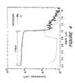
- FIG. 4shows a SIMS profile of a GaN:Mg layer where the presence of O at the interface can be clearly seen.
- FIG. 5illustrates the depth profile for Mg of a prior art LED.
- FIG. 6illustrates the depth profile for Mg using the method of the present invention.
- FIG. 3illustrates an embodiment of the present invention 10 .
- An interfacial layer 16is added to a light-emitting diode or laser diode structure to performs the role of strain engineering and impurity gettering.
- a layer of Al x In y Ga 1 ⁇ x ⁇ y N (0 ⁇ x ⁇ 1, 0 ⁇ y ⁇ 1) doped with Mg, Zn, Cdcan be used for the interfacial layer.
- the interfacial layermay be undoped.
- the interfacial layercan also include alloys of AlInGaN, AlInGaP, and AlInGaAs, and alloys of GaN, GaP, and GaAs.
- the interfacial layer 16is deposited directly on top of the buffer layer 14 prior to the growth of the n-type (GaN:Si) layer 18 , active region 10 , and the p-type layer 22 .
- the thickness of the interfacial layervaries from 0.01-10.0 ⁇ m, having a preferred thickness range of 0.25-1.0 ⁇ m.
- Buffer layer 14is formed over a substrate 12 .
- Substrate 12maybe transparent.
- Metal contact layers 24 A, 24 Bare deposited to the p-type and n-type layers 22 , 18 , respectively.
- the interfacial layerincreases device reliability and reproducibility by “gettering” or trapping the residual impurities, e.g., oxygen, in the initial layer of the structure.
- the processalso cleanses the chamber and the reactor components making them free of further impurities which would be present later when the more critical layers, e.g., the active layer or the p-type layers, in the structure are grown.
- the preferred embodimentuses GaN:Mg and/or AlGaN for the composition of the interfacial layer because both Mg and Al have a high affinity for oxygen.
- the sources that are affected adversely by the presence of oxygen-containing impuritiese.g. those containing Mg, Zn, and Al, are easier to use and less prone to pre-reactions and, ultimately, gas-phase depletion after the interfacial layer is grown.
- FIG. 4shows a secondary ion mass spectrometry (SIMS) profile of a GaN:Mg layer where the presence of oxygen at the interface can be clearly seen. After the first 0.25-0.35 ⁇ m, the concentration of oxygen is reduced to the SIMS background level, indicating that the oxygen has been trapped in this non-critical portion of the structure.
- FIG. 5shows the Mg profile in a GaN-based LED. The Mg-doped region on the right side of the figure is the interfacial layer described in this invention. The In profile is provided as a marker, indicating the location of the active region.
- Sihas a smaller atomic radius than that of Ga (0.41 vs. 0.62 ⁇ ), which Si displaces from the lattice.
- Films doped with Siare grown in a state of tension, an unfavorable state for brittle materials, e.g. GaN.
- Mgis often a difficult impurity to control during crystal growth.
- the chemical profile for Mgtakes an extended time and substantial film thickness before reaching an equilibrium concentration. Since the carrier mobility and lifetime for holes in GaN:Mg are generally low, the placement of Mg, and hence the location of the p-n junction is critical for efficient LED operation. Since the thickness of the interfacial layer is generally larger than the thickness required to achieve the equilibrium concentration of magnesium, the present invention can be used to greatly reduce the time needed to reach equilibrium concentration.
Landscapes
- Physics & Mathematics (AREA)
- Condensed Matter Physics & Semiconductors (AREA)
- General Physics & Mathematics (AREA)
- Electromagnetism (AREA)
- Optics & Photonics (AREA)
- Led Devices (AREA)
- Semiconductor Lasers (AREA)
- Recrystallisation Techniques (AREA)
Abstract
Description
| TABLE I |
| Properties of the nitrides and selected substrates |
| Material |
| GaN | AlN | InN | sapphire | 6H-SiC | ||
| Lattice Constant (Å) | |||||
| a | 3.189 | 3.112 | 3.548 | 4.758 | 3.08 |
| c | 5.185 | 4.982 | 5.76 | 12.991 | 15.12 |
| Thermal Expansion | |||||
| Coefficient | |||||
| (/K−1) | |||||
| a | 5.59 × 10⁻⁶ | 4.2 × 10⁻⁶ | 4 × 10⁻⁶ | 7.5 × 10⁻⁶ | 4.2 × 10⁻⁶ |
| c | 3.17 × 10⁻⁶ | 5.3 × 10⁻⁶ | 3 × 10⁻⁶ | 8.5 × 10⁻⁶ | 4.68 × 10⁻⁶ |
Claims (11)
Priority Applications (1)
| Application Number | Priority Date | Filing Date | Title |
|---|---|---|---|
| US09/655,752US6274399B1 (en) | 1998-06-05 | 2000-09-06 | Method of strain engineering and impurity control in III-V nitride semiconductor films and optoelectronic devices |
Applications Claiming Priority (2)
| Application Number | Priority Date | Filing Date | Title |
|---|---|---|---|
| US09/092,478US6194742B1 (en) | 1998-06-05 | 1998-06-05 | Strain engineered and impurity controlled III-V nitride semiconductor films and optoelectronic devices |
| US09/655,752US6274399B1 (en) | 1998-06-05 | 2000-09-06 | Method of strain engineering and impurity control in III-V nitride semiconductor films and optoelectronic devices |
Related Parent Applications (1)
| Application Number | Title | Priority Date | Filing Date |
|---|---|---|---|
| US09/092,478DivisionUS6194742B1 (en) | 1998-06-05 | 1998-06-05 | Strain engineered and impurity controlled III-V nitride semiconductor films and optoelectronic devices |
Publications (1)
| Publication Number | Publication Date |
|---|---|
| US6274399B1true US6274399B1 (en) | 2001-08-14 |
Family
ID=22233422
Family Applications (2)
| Application Number | Title | Priority Date | Filing Date |
|---|---|---|---|
| US09/092,478Expired - LifetimeUS6194742B1 (en) | 1998-06-05 | 1998-06-05 | Strain engineered and impurity controlled III-V nitride semiconductor films and optoelectronic devices |
| US09/655,752Expired - LifetimeUS6274399B1 (en) | 1998-06-05 | 2000-09-06 | Method of strain engineering and impurity control in III-V nitride semiconductor films and optoelectronic devices |
Family Applications Before (1)
| Application Number | Title | Priority Date | Filing Date |
|---|---|---|---|
| US09/092,478Expired - LifetimeUS6194742B1 (en) | 1998-06-05 | 1998-06-05 | Strain engineered and impurity controlled III-V nitride semiconductor films and optoelectronic devices |
Country Status (4)
| Country | Link |
|---|---|
| US (2) | US6194742B1 (en) |
| JP (1) | JP4677065B2 (en) |
| DE (1) | DE19905516C2 (en) |
| GB (1) | GB2338109A (en) |
Cited By (41)
| Publication number | Priority date | Publication date | Assignee | Title |
|---|---|---|---|---|
| WO2004114421A1 (en)* | 2003-06-25 | 2004-12-29 | Lg Innotek Co.,Ltd | A light emitting device using nitride semiconductor and fabrication method of the same |
| US6865201B2 (en)* | 2001-03-23 | 2005-03-08 | Sharp Kabushiki Kaisha | Semiconductor laser device, method of fabricating the same and optical information reproduction apparatus |
| US20050139818A1 (en)* | 2003-12-24 | 2005-06-30 | Lee Jae H. | Gallium nitride semiconductor light emitting device and method of manufacturing the same |
| US6949395B2 (en)* | 2001-10-22 | 2005-09-27 | Oriol, Inc. | Method of making diode having reflective layer |
| EP1657758A2 (en) | 2004-11-15 | 2006-05-17 | LumiLeds Lighting U.S., LLC | Light emitting diode with molded lens and method of manufacturing the same |
| US20060102914A1 (en)* | 2004-11-15 | 2006-05-18 | Lumileds Lighting U.S., Llc | Wide emitting lens for LED useful for backlighting |
| US20060105484A1 (en)* | 2004-11-15 | 2006-05-18 | Grigoriy Basin | Molded lens over LED die |
| US20060220031A1 (en)* | 2005-04-05 | 2006-10-05 | Lumileds Lighting U.S., Llc | A1lnGaP LED having reduced temperature dependence |
| US20060243986A1 (en)* | 2005-04-29 | 2006-11-02 | Lumileds Lighting U.S., Llc | RGB thermal isolation substrate |
| US20070076412A1 (en)* | 2005-09-30 | 2007-04-05 | Lumileds Lighting U.S., Llc | Light source with light emitting array and collection optic |
| US20070081336A1 (en)* | 2005-10-11 | 2007-04-12 | Bierhuizen Serge J | Illumination system with optical concentrator and wavelength converting element |
| US20080048200A1 (en)* | 2004-11-15 | 2008-02-28 | Philips Lumileds Lighting Company, Llc | LED with Phosphor Tile and Overmolded Phosphor in Lens |
| US20080153191A1 (en)* | 2006-12-22 | 2008-06-26 | Philips Lumileds Lighting Company, Llc | III-Nitride Light Emitting Devices Grown on Templates to Reduce Strain |
| US20090230409A1 (en)* | 2008-03-17 | 2009-09-17 | Philips Lumileds Lighting Company, Llc | Underfill process for flip-chip leds |
| US20100012956A1 (en)* | 2001-07-17 | 2010-01-21 | Yoo Myung Cheol | Diode having high brightness and method thereof |
| US20100019225A1 (en)* | 2002-08-19 | 2010-01-28 | Suk Hun Lee | Nitride semiconductor led and fabrication method thereof |
| US20100065864A1 (en)* | 2008-09-18 | 2010-03-18 | Koninklijke Philips Electronics N.V. | White point compensated leds for lcd displays |
| US20110012149A1 (en)* | 2009-07-16 | 2011-01-20 | Koninklijke Philips Electronics N.V. | Reflective substratefor leds |
| WO2011015959A1 (en) | 2009-08-07 | 2011-02-10 | Philips Lumileds Lighting Company, Llc | Led with silicone layer and laminated remote phosphor layer |
| US20110049545A1 (en)* | 2009-09-02 | 2011-03-03 | Koninklijke Philips Electronics N.V. | Led package with phosphor plate and reflective substrate |
| EP1589593A3 (en)* | 2004-04-21 | 2011-04-27 | Philips Lumileds Lighting Company LLC | Strain-controlled III-Nitride light emitting device |
| WO2011135528A1 (en) | 2010-04-30 | 2011-11-03 | Koninklijke Philips Electronics N.V. | Led wafer with laminated phosphor layer |
| WO2012023119A1 (en) | 2010-08-20 | 2012-02-23 | Koninklijke Philips Electronics N.V. | Lamination process for leds |
| US20120241821A1 (en)* | 2009-12-01 | 2012-09-27 | Soitec | Heterostructure for electronic power components, optoelectronic or photovoltaic components |
| WO2013144919A1 (en) | 2012-03-29 | 2013-10-03 | Koninklijke Philips N.V. | Phosphor in inorganic binder for led applications |
| WO2013144777A1 (en) | 2012-03-29 | 2013-10-03 | Koninklijke Philips N.V. | Phosphor in inorganic binder for led applications |
| WO2014006539A1 (en) | 2012-07-05 | 2014-01-09 | Koninklijke Philips N.V. | Phosphor separated from led by transparent spacer |
| US8629475B2 (en) | 2012-01-24 | 2014-01-14 | Cooledge Lighting Inc. | Light-emitting dies incorporating wavelength-conversion materials and related methods |
| US8896010B2 (en) | 2012-01-24 | 2014-11-25 | Cooledge Lighting Inc. | Wafer-level flip chip device packages and related methods |
| US8907362B2 (en) | 2012-01-24 | 2014-12-09 | Cooledge Lighting Inc. | Light-emitting dies incorporating wavelength-conversion materials and related methods |
| US9000468B2 (en) | 2001-10-26 | 2015-04-07 | Lg Innotek Co., Ltd. | Diode having vertical structure |
| US9343443B2 (en) | 2014-02-05 | 2016-05-17 | Cooledge Lighting, Inc. | Light-emitting dies incorporating wavelength-conversion materials and related methods |
| WO2017047011A1 (en)* | 2015-09-15 | 2017-03-23 | 信越半導体株式会社 | Method of mounting light-emitting element |
| US20170274474A1 (en)* | 2014-08-19 | 2017-09-28 | Koninklijke Philips N.V. | Sapphire collector for reducing mechanical damage during die level laser lift-off |
| US20180261715A1 (en)* | 2015-05-13 | 2018-09-13 | Koninklijke Philips N.V. | Sapphire collector for reducing mechanical damage during die level laser lift-off |
| US20190237638A1 (en) | 2016-07-26 | 2019-08-01 | Cree, Inc. | Light emitting diodes, components and related methods |
| US20190363223A1 (en)* | 2018-05-25 | 2019-11-28 | Cree, Inc. | Light-emitting diode packages |
| USD902448S1 (en) | 2018-08-31 | 2020-11-17 | Cree, Inc. | Light emitting diode package |
| US11101411B2 (en) | 2019-06-26 | 2021-08-24 | Creeled, Inc. | Solid-state light emitting devices including light emitting diodes in package structures |
| US11233183B2 (en) | 2018-08-31 | 2022-01-25 | Creeled, Inc. | Light-emitting diodes, light-emitting diode arrays and related devices |
| US11335833B2 (en) | 2018-08-31 | 2022-05-17 | Creeled, Inc. | Light-emitting diodes, light-emitting diode arrays and related devices |
Families Citing this family (46)
| Publication number | Priority date | Publication date | Assignee | Title |
|---|---|---|---|---|
| JP3770014B2 (en)* | 1999-02-09 | 2006-04-26 | 日亜化学工業株式会社 | Nitride semiconductor device |
| US6133589A (en)* | 1999-06-08 | 2000-10-17 | Lumileds Lighting, U.S., Llc | AlGaInN-based LED having thick epitaxial layer for improved light extraction |
| US6465809B1 (en) | 1999-06-09 | 2002-10-15 | Kabushiki Kaisha Toshiba | Bonding type semiconductor substrate, semiconductor light emitting element, and preparation process thereof |
| JP4576674B2 (en)* | 2000-06-26 | 2010-11-10 | 豊田合成株式会社 | Group III nitride compound semiconductor device |
| US6841808B2 (en)* | 2000-06-23 | 2005-01-11 | Toyoda Gosei Co., Ltd. | Group III nitride compound semiconductor device and method for producing the same |
| GB2365208A (en)* | 2000-07-19 | 2002-02-13 | Juses Chao | Amorphous alingan light emitting diode |
| DE10056475B4 (en)* | 2000-11-15 | 2010-10-07 | Osram Opto Semiconductors Gmbh | GaN-based radiation-emitting semiconductor device with improved p-type conductivity and method for its production |
| US6791119B2 (en)* | 2001-02-01 | 2004-09-14 | Cree, Inc. | Light emitting diodes including modifications for light extraction |
| US6794684B2 (en) | 2001-02-01 | 2004-09-21 | Cree, Inc. | Reflective ohmic contacts for silicon carbide including a layer consisting essentially of nickel, methods of fabricating same, and light emitting devices including the same |
| US6653166B2 (en)* | 2001-05-09 | 2003-11-25 | Nsc-Nanosemiconductor Gmbh | Semiconductor device and method of making same |
| US6784074B2 (en) | 2001-05-09 | 2004-08-31 | Nsc-Nanosemiconductor Gmbh | Defect-free semiconductor templates for epitaxial growth and method of making same |
| US6630692B2 (en)* | 2001-05-29 | 2003-10-07 | Lumileds Lighting U.S., Llc | III-Nitride light emitting devices with low driving voltage |
| US7211833B2 (en) | 2001-07-23 | 2007-05-01 | Cree, Inc. | Light emitting diodes including barrier layers/sublayers |
| US6740906B2 (en)* | 2001-07-23 | 2004-05-25 | Cree, Inc. | Light emitting diodes including modifications for submount bonding |
| US20030090103A1 (en)* | 2001-11-09 | 2003-05-15 | Thomas Becker | Direct mailing device |
| US7030428B2 (en) | 2001-12-03 | 2006-04-18 | Cree, Inc. | Strain balanced nitride heterojunction transistors |
| KR101017657B1 (en)* | 2002-04-30 | 2011-02-25 | 크리 인코포레이티드 | High voltage switching device and manufacturing method thereof |
| US6841001B2 (en) | 2002-07-19 | 2005-01-11 | Cree, Inc. | Strain compensated semiconductor structures and methods of fabricating strain compensated semiconductor structures |
| US20060048700A1 (en)* | 2002-09-05 | 2006-03-09 | Wanlass Mark W | Method for achieving device-quality, lattice-mismatched, heteroepitaxial active layers |
| US6943381B2 (en)* | 2004-01-30 | 2005-09-13 | Lumileds Lighting U.S., Llc | III-nitride light-emitting devices with improved high-current efficiency |
| US7119374B2 (en)* | 2004-02-20 | 2006-10-10 | Supernova Optoelectronics Corp. | Gallium nitride based light emitting device and the fabricating method for the same |
| JP2007081180A (en)* | 2005-09-15 | 2007-03-29 | Matsushita Electric Ind Co Ltd | Semiconductor light emitting device |
| US20070069225A1 (en)* | 2005-09-27 | 2007-03-29 | Lumileds Lighting U.S., Llc | III-V light emitting device |
| US8334155B2 (en)* | 2005-09-27 | 2012-12-18 | Philips Lumileds Lighting Company Llc | Substrate for growing a III-V light emitting device |
| US7772604B2 (en) | 2006-01-05 | 2010-08-10 | Illumitex | Separate optical device for directing light from an LED |
| WO2008042351A2 (en)* | 2006-10-02 | 2008-04-10 | Illumitex, Inc. | Led system and method |
| US20090275266A1 (en)* | 2006-10-02 | 2009-11-05 | Illumitex, Inc. | Optical device polishing |
| JP2011512037A (en)* | 2008-02-08 | 2011-04-14 | イルミテックス, インコーポレイテッド | System and method for emitter layer shaping |
| US9048169B2 (en)* | 2008-05-23 | 2015-06-02 | Soitec | Formation of substantially pit free indium gallium nitride |
| US8431419B2 (en)* | 2008-08-28 | 2013-04-30 | Soitec | UV absorption based monitor and control of chloride gas stream |
| TW201034256A (en)* | 2008-12-11 | 2010-09-16 | Illumitex Inc | Systems and methods for packaging light-emitting diode devices |
| US8449128B2 (en)* | 2009-08-20 | 2013-05-28 | Illumitex, Inc. | System and method for a lens and phosphor layer |
| US8585253B2 (en) | 2009-08-20 | 2013-11-19 | Illumitex, Inc. | System and method for color mixing lens array |
| US20110057213A1 (en)* | 2009-09-08 | 2011-03-10 | Koninklijke Philips Electronics N.V. | Iii-nitride light emitting device with curvat1jre control layer |
| US8436363B2 (en) | 2011-02-03 | 2013-05-07 | Soitec | Metallic carrier for layer transfer and methods for forming the same |
| US9082948B2 (en) | 2011-02-03 | 2015-07-14 | Soitec | Methods of fabricating semiconductor structures using thermal spray processes, and semiconductor structures fabricated using such methods |
| US9142412B2 (en) | 2011-02-03 | 2015-09-22 | Soitec | Semiconductor devices including substrate layers and overlying semiconductor layers having closely matching coefficients of thermal expansion, and related methods |
| WO2013129572A1 (en)* | 2012-02-29 | 2013-09-06 | 京セラ株式会社 | Composite substrate |
| US9312432B2 (en)* | 2012-03-13 | 2016-04-12 | Tsmc Solid State Lighting Ltd. | Growing an improved P-GaN layer of an LED through pressure ramping |
| CN104412395B (en)* | 2012-07-11 | 2018-07-17 | 亮锐控股有限公司 | Reduce or eliminate nanotube defects in III-nitride structures |
| JP6223075B2 (en)* | 2012-10-09 | 2017-11-01 | キヤノン株式会社 | Light emitting device manufacturing method and light emitting device |
| WO2014057748A1 (en)* | 2012-10-12 | 2014-04-17 | 住友電気工業株式会社 | Group iii nitride composite substrate, manufacturing method therefor, and group iii nitride semiconductor device manufacturing method |
| US9412911B2 (en) | 2013-07-09 | 2016-08-09 | The Silanna Group Pty Ltd | Optical tuning of light emitting semiconductor junctions |
| CN104733576B (en)* | 2015-02-28 | 2017-07-25 | 华灿光电(苏州)有限公司 | Light-emitting diode epitaxial wafer and preparation method thereof |
| US9873170B2 (en) | 2015-03-24 | 2018-01-23 | Nichia Corporation | Method of manufacturing light emitting element |
| JP6146455B2 (en)* | 2015-03-24 | 2017-06-14 | 日亜化学工業株式会社 | Method for manufacturing light emitting device |
Citations (22)
| Publication number | Priority date | Publication date | Assignee | Title |
|---|---|---|---|---|
| JPH01103998A (en)* | 1987-10-16 | 1989-04-21 | Furukawa Electric Co Ltd:The | Formation of iii-v compound semiconductor p-type crystal |
| JPH01212483A (en)* | 1988-02-19 | 1989-08-25 | Nec Corp | Semiconductor device |
| US5436466A (en) | 1992-08-19 | 1995-07-25 | Goldstar Co., Ltd. | Semiconductor laser diode |
| US5458085A (en)* | 1992-03-04 | 1995-10-17 | Fujitsu Limited | Magnesium-doping in III-V compound semiconductor |
| US5488233A (en) | 1993-03-11 | 1996-01-30 | Kabushiki Kaisha Toshiba | Semiconductor light-emitting device with compound semiconductor layer |
| EP0731512A2 (en) | 1995-03-10 | 1996-09-11 | Hewlett-Packard Company | Light emitting diode |
| US5665986A (en) | 1995-03-27 | 1997-09-09 | Sumitomo Electric Industries, Ltd. | Compound semiconductor light emitting device and method of preparing the same |
| US5670798A (en) | 1995-03-29 | 1997-09-23 | North Carolina State University | Integrated heterostructures of Group III-V nitride semiconductor materials including epitaxial ohmic contact non-nitride buffer layer and methods of fabricating same |
| JPH1033988A (en)* | 1996-07-24 | 1998-02-10 | Miki Riken Kogyo Kk | Inorganic oxide composite and its producing process |
| US5729029A (en) | 1996-09-06 | 1998-03-17 | Hewlett-Packard Company | Maximizing electrical doping while reducing material cracking in III-V nitride semiconductor devices |
| US5732098A (en) | 1995-04-14 | 1998-03-24 | Kabushiki Kaisha Toshiba | LED display device |
| US5741724A (en)* | 1996-12-27 | 1998-04-21 | Motorola | Method of growing gallium nitride on a spinel substrate |
| US5751021A (en) | 1995-04-24 | 1998-05-12 | Sharp Kk | Semiconductor light-emitting device |
| US5793061A (en) | 1995-08-28 | 1998-08-11 | Mitsubishi Cable Industries, Ltd. | Group-III nitride based light emitter |
| US5815520A (en) | 1995-07-27 | 1998-09-29 | Nec Corporation | light emitting semiconductor device and its manufacturing method |
| US5814838A (en) | 1996-05-22 | 1998-09-29 | Sanken Electric Co., Ltd. | Light emitting semiconductor element with ZN doping |
| US5863811A (en)* | 1995-06-28 | 1999-01-26 | Sony Corporation | Method for growing single crystal III-V compound semiconductor layers on non single crystal III-V Compound semiconductor buffer layers |
| US5874320A (en)* | 1997-03-20 | 1999-02-23 | Industrial Technology Research Institute | Method for forming P-type gallium nitride |
| US5929466A (en) | 1994-03-09 | 1999-07-27 | Kabushiki Kaisha Toshiba | Semiconductor device and method of fabricating the same |
| US5963787A (en)* | 1997-07-15 | 1999-10-05 | Nec Corporation | Method of producing gallium nitride semiconductor light emitting device |
| US6081001A (en) | 1996-03-14 | 2000-06-27 | Sony Corporation | Nitride semiconductor light emitting device |
| US6146916A (en)* | 1997-12-02 | 2000-11-14 | Murata Manufacturing Co., Ltd. | Method for forming a GaN-based semiconductor light emitting device |
Family Cites Families (8)
| Publication number | Priority date | Publication date | Assignee | Title |
|---|---|---|---|---|
| JPS63198320A (en)* | 1987-02-13 | 1988-08-17 | Mitsubishi Electric Corp | Crystal growth method |
| JPS6484773A (en)* | 1987-09-28 | 1989-03-30 | Mitsubishi Electric Corp | Semiconductor laser device and manufacture thereof |
| JP2653562B2 (en)* | 1991-02-05 | 1997-09-17 | 三菱電機株式会社 | Semiconductor laser and method of manufacturing the same |
| JPH05175607A (en)* | 1991-06-18 | 1993-07-13 | Matsushita Electric Ind Co Ltd | Method of forming semiconductor multilayer film and manufacture of semiconductor laser |
| JPH07176821A (en)* | 1993-12-20 | 1995-07-14 | Matsushita Electric Ind Co Ltd | Semiconductor laser device and manufacturing method thereof |
| JPH08167392A (en)* | 1994-12-13 | 1996-06-25 | Canon Inc | Image display device and manufacturing method thereof |
| JPH1065271A (en)* | 1996-08-13 | 1998-03-06 | Toshiba Corp | Gallium nitride based semiconductor light emitting device |
| JPH10150245A (en)* | 1996-11-21 | 1998-06-02 | Matsushita Electric Ind Co Ltd | Manufacturing method of gallium nitride based semiconductor |
- 1998
- 1998-06-05USUS09/092,478patent/US6194742B1/ennot_activeExpired - Lifetime
- 1999
- 1999-02-10DEDE19905516Apatent/DE19905516C2/ennot_activeExpired - Lifetime
- 1999-06-02JPJP15495799Apatent/JP4677065B2/ennot_activeExpired - Lifetime
- 1999-06-03GBGB9912940Apatent/GB2338109A/ennot_activeWithdrawn
- 2000
- 2000-09-06USUS09/655,752patent/US6274399B1/ennot_activeExpired - Lifetime
Patent Citations (22)
| Publication number | Priority date | Publication date | Assignee | Title |
|---|---|---|---|---|
| JPH01103998A (en)* | 1987-10-16 | 1989-04-21 | Furukawa Electric Co Ltd:The | Formation of iii-v compound semiconductor p-type crystal |
| JPH01212483A (en)* | 1988-02-19 | 1989-08-25 | Nec Corp | Semiconductor device |
| US5458085A (en)* | 1992-03-04 | 1995-10-17 | Fujitsu Limited | Magnesium-doping in III-V compound semiconductor |
| US5436466A (en) | 1992-08-19 | 1995-07-25 | Goldstar Co., Ltd. | Semiconductor laser diode |
| US5488233A (en) | 1993-03-11 | 1996-01-30 | Kabushiki Kaisha Toshiba | Semiconductor light-emitting device with compound semiconductor layer |
| US5929466A (en) | 1994-03-09 | 1999-07-27 | Kabushiki Kaisha Toshiba | Semiconductor device and method of fabricating the same |
| EP0731512A2 (en) | 1995-03-10 | 1996-09-11 | Hewlett-Packard Company | Light emitting diode |
| US5665986A (en) | 1995-03-27 | 1997-09-09 | Sumitomo Electric Industries, Ltd. | Compound semiconductor light emitting device and method of preparing the same |
| US5670798A (en) | 1995-03-29 | 1997-09-23 | North Carolina State University | Integrated heterostructures of Group III-V nitride semiconductor materials including epitaxial ohmic contact non-nitride buffer layer and methods of fabricating same |
| US5732098A (en) | 1995-04-14 | 1998-03-24 | Kabushiki Kaisha Toshiba | LED display device |
| US5751021A (en) | 1995-04-24 | 1998-05-12 | Sharp Kk | Semiconductor light-emitting device |
| US5863811A (en)* | 1995-06-28 | 1999-01-26 | Sony Corporation | Method for growing single crystal III-V compound semiconductor layers on non single crystal III-V Compound semiconductor buffer layers |
| US5815520A (en) | 1995-07-27 | 1998-09-29 | Nec Corporation | light emitting semiconductor device and its manufacturing method |
| US5793061A (en) | 1995-08-28 | 1998-08-11 | Mitsubishi Cable Industries, Ltd. | Group-III nitride based light emitter |
| US6081001A (en) | 1996-03-14 | 2000-06-27 | Sony Corporation | Nitride semiconductor light emitting device |
| US5814838A (en) | 1996-05-22 | 1998-09-29 | Sanken Electric Co., Ltd. | Light emitting semiconductor element with ZN doping |
| JPH1033988A (en)* | 1996-07-24 | 1998-02-10 | Miki Riken Kogyo Kk | Inorganic oxide composite and its producing process |
| US5729029A (en) | 1996-09-06 | 1998-03-17 | Hewlett-Packard Company | Maximizing electrical doping while reducing material cracking in III-V nitride semiconductor devices |
| US5741724A (en)* | 1996-12-27 | 1998-04-21 | Motorola | Method of growing gallium nitride on a spinel substrate |
| US5874320A (en)* | 1997-03-20 | 1999-02-23 | Industrial Technology Research Institute | Method for forming P-type gallium nitride |
| US5963787A (en)* | 1997-07-15 | 1999-10-05 | Nec Corporation | Method of producing gallium nitride semiconductor light emitting device |
| US6146916A (en)* | 1997-12-02 | 2000-11-14 | Murata Manufacturing Co., Ltd. | Method for forming a GaN-based semiconductor light emitting device |
Non-Patent Citations (1)
| Title |
|---|
| T. Hayakawa et al., "Improvements in AIGaAs laser diodes grown by molecular beam epitaxy using a compositionally graded buffer layer", Appl. Phys. Lett. vol. 49, No. 4, Jul. 28, 1986, pp. 191-193. |
Cited By (113)
| Publication number | Priority date | Publication date | Assignee | Title |
|---|---|---|---|---|
| US6865201B2 (en)* | 2001-03-23 | 2005-03-08 | Sharp Kabushiki Kaisha | Semiconductor laser device, method of fabricating the same and optical information reproduction apparatus |
| US9136424B2 (en) | 2001-07-17 | 2015-09-15 | Lg Innotek Co., Ltd. | Diode having high brightness and method thereof |
| US10553744B2 (en) | 2001-07-17 | 2020-02-04 | Lg Innotek Co., Ltd. | Diode having high brightness and method thereof |
| US10147841B2 (en) | 2001-07-17 | 2018-12-04 | Lg Innotek Co., Ltd. | Diode having high brightness and method thereof |
| US9640713B2 (en) | 2001-07-17 | 2017-05-02 | Lg Innotek Co., Ltd. | Diode having high brightness and method thereof |
| US8674386B2 (en) | 2001-07-17 | 2014-03-18 | Lg Innotek Co. Ltd. | Diode having high brightness and method thereof |
| US7939849B2 (en) | 2001-07-17 | 2011-05-10 | Lg Electronics Inc. | Diode having high brightness and method thereof |
| US20100012956A1 (en)* | 2001-07-17 | 2010-01-21 | Yoo Myung Cheol | Diode having high brightness and method thereof |
| US8759129B2 (en) | 2001-10-22 | 2014-06-24 | Lg Innotek Co., Ltd | Method of making diode having reflective layer |
| US20100285621A1 (en)* | 2001-10-22 | 2010-11-11 | Yoo Myung Cheol | Method of making diode having reflective layer |
| US7682854B2 (en) | 2001-10-22 | 2010-03-23 | Lg Electronics Inc. | Method of making diode having reflective layer |
| US7785908B2 (en) | 2001-10-22 | 2010-08-31 | Lg Electronics Inc. | Method of making diode having reflective layer |
| US8236585B2 (en) | 2001-10-22 | 2012-08-07 | Lg Electronics Inc. | Method of making diode having reflective layer |
| US9406837B2 (en) | 2001-10-22 | 2016-08-02 | Lg Innotek Co., Ltd | Method of making diode having reflective layer |
| US6949395B2 (en)* | 2001-10-22 | 2005-09-27 | Oriol, Inc. | Method of making diode having reflective layer |
| US20070172973A1 (en)* | 2001-10-22 | 2007-07-26 | Yoo Myung C | Method of making diode having reflective layer |
| US20060006400A1 (en)* | 2001-10-22 | 2006-01-12 | Yoo Myung C | Method of making diode having reflective layer |
| US9620677B2 (en) | 2001-10-26 | 2017-04-11 | Lg Innotek Co., Ltd. | Diode having vertical structure |
| US10032959B2 (en) | 2001-10-26 | 2018-07-24 | Lg Innotek Co., Ltd. | Diode having vertical structure |
| US10326055B2 (en) | 2001-10-26 | 2019-06-18 | Lg Innotek Co., Ltd. | Diode having vertical structure |
| US9000468B2 (en) | 2001-10-26 | 2015-04-07 | Lg Innotek Co., Ltd. | Diode having vertical structure |
| US8492779B2 (en) | 2002-08-19 | 2013-07-23 | Lg Innotek Co., Ltd. | Nitride semiconductor LED and fabrication method thereof |
| US20100019225A1 (en)* | 2002-08-19 | 2010-01-28 | Suk Hun Lee | Nitride semiconductor led and fabrication method thereof |
| US20060081831A1 (en)* | 2003-06-25 | 2006-04-20 | Lee Suk H | Light emitting device using nitride semiconductor and fabrication method of the same |
| US20050236631A1 (en)* | 2003-06-25 | 2005-10-27 | Lee Suk H | Light emitting device using nitride semiconductor and fabrication method of the same |
| US7193236B2 (en) | 2003-06-25 | 2007-03-20 | Lg Innotek Co., Ltd | Light emitting device using nitride semiconductor and fabrication method of the same |
| US7691657B2 (en) | 2003-06-25 | 2010-04-06 | Lg Innotek Co., Ltd. | Light emitting device using nitride semiconductor and fabrication method of the same |
| WO2004114421A1 (en)* | 2003-06-25 | 2004-12-29 | Lg Innotek Co.,Ltd | A light emitting device using nitride semiconductor and fabrication method of the same |
| US20050139818A1 (en)* | 2003-12-24 | 2005-06-30 | Lee Jae H. | Gallium nitride semiconductor light emitting device and method of manufacturing the same |
| EP1589593A3 (en)* | 2004-04-21 | 2011-04-27 | Philips Lumileds Lighting Company LLC | Strain-controlled III-Nitride light emitting device |
| US7452737B2 (en) | 2004-11-15 | 2008-11-18 | Philips Lumileds Lighting Company, Llc | Molded lens over LED die |
| EP1657758A2 (en) | 2004-11-15 | 2006-05-17 | LumiLeds Lighting U.S., LLC | Light emitting diode with molded lens and method of manufacturing the same |
| US20060102914A1 (en)* | 2004-11-15 | 2006-05-18 | Lumileds Lighting U.S., Llc | Wide emitting lens for LED useful for backlighting |
| US9081167B2 (en) | 2004-11-15 | 2015-07-14 | Koninklijke Philips N.V. | Lens compression molded over LED die |
| US20060105484A1 (en)* | 2004-11-15 | 2006-05-18 | Grigoriy Basin | Molded lens over LED die |
| US20080048200A1 (en)* | 2004-11-15 | 2008-02-28 | Philips Lumileds Lighting Company, Llc | LED with Phosphor Tile and Overmolded Phosphor in Lens |
| US7858408B2 (en) | 2004-11-15 | 2010-12-28 | Koninklijke Philips Electronics N.V. | LED with phosphor tile and overmolded phosphor in lens |
| EP2448021A2 (en) | 2004-11-15 | 2012-05-02 | Philips Lumileds Lighting Company, LLC. | Molding a lens over a LED die |
| EP2448022A2 (en) | 2004-11-15 | 2012-05-02 | Philips Lumileds Lighting Company, LLC. | Molding a lens over a LED die |
| US20080157114A1 (en)* | 2004-11-15 | 2008-07-03 | Philips Lumileds Lighting Company, Llc | Multiple Lenses Molded Over LED Die |
| US20110057205A1 (en)* | 2004-11-15 | 2011-03-10 | Koninklijke Philips Electronics N.V. | Led with phosphor tile and overmolded phosphor in lens |
| US7352011B2 (en) | 2004-11-15 | 2008-04-01 | Philips Lumileds Lighting Company, Llc | Wide emitting lens for LED useful for backlighting |
| WO2006103582A1 (en) | 2005-03-29 | 2006-10-05 | Koninklijke Philips Electronics N.V. | Wide emitting lens for led useful for backlighting |
| WO2006106467A1 (en) | 2005-04-05 | 2006-10-12 | Koninklijke Philips Electronics N.V. | Allngap led having reduced temperature dependence |
| US7863631B2 (en) | 2005-04-05 | 2011-01-04 | Koninklijke Philips Electronics N.V. | A1InGaP LED having reduced temperature dependence |
| US7244630B2 (en) | 2005-04-05 | 2007-07-17 | Philips Lumileds Lighting Company, Llc | A1InGaP LED having reduced temperature dependence |
| US20070131961A1 (en)* | 2005-04-05 | 2007-06-14 | Philips Lumileds Lighting Company, Llc | AlInGaP LED Having Reduced Temperature Dependence |
| US7544525B2 (en) | 2005-04-05 | 2009-06-09 | Philips Lumileds Lighting Co., Llc | AllnGaP LED having reduced temperature dependence |
| US20060220031A1 (en)* | 2005-04-05 | 2006-10-05 | Lumileds Lighting U.S., Llc | A1lnGaP LED having reduced temperature dependence |
| US20090230381A1 (en)* | 2005-04-05 | 2009-09-17 | Koninklijke Philips Electronics N.V. | AlInGaP LED HAVING REDUCED TEMPERATURE DEPENDENCE |
| US7952112B2 (en) | 2005-04-29 | 2011-05-31 | Philips Lumileds Lighting Company Llc | RGB thermal isolation substrate |
| US20060243986A1 (en)* | 2005-04-29 | 2006-11-02 | Lumileds Lighting U.S., Llc | RGB thermal isolation substrate |
| US20070076412A1 (en)* | 2005-09-30 | 2007-04-05 | Lumileds Lighting U.S., Llc | Light source with light emitting array and collection optic |
| US7543959B2 (en) | 2005-10-11 | 2009-06-09 | Philips Lumiled Lighting Company, Llc | Illumination system with optical concentrator and wavelength converting element |
| US20070081336A1 (en)* | 2005-10-11 | 2007-04-12 | Bierhuizen Serge J | Illumination system with optical concentrator and wavelength converting element |
| US7534638B2 (en)* | 2006-12-22 | 2009-05-19 | Philips Lumiled Lighting Co., Llc | III-nitride light emitting devices grown on templates to reduce strain |
| US20080153191A1 (en)* | 2006-12-22 | 2008-06-26 | Philips Lumileds Lighting Company, Llc | III-Nitride Light Emitting Devices Grown on Templates to Reduce Strain |
| TWI452717B (en)* | 2006-12-22 | 2014-09-11 | Philips Lumileds Lighting Co | Group III nitride light-emitting device grown on a template to reduce strain |
| US20110223696A1 (en)* | 2008-03-17 | 2011-09-15 | Koninklijke Philips Electronics N.V. | Underfill process for flip-chip leds |
| US8273587B2 (en) | 2008-03-17 | 2012-09-25 | Lumileds Lighting Company Llc | Underfill process for flip-chip LEDs |
| US20090230409A1 (en)* | 2008-03-17 | 2009-09-17 | Philips Lumileds Lighting Company, Llc | Underfill process for flip-chip leds |
| US7858409B2 (en)* | 2008-09-18 | 2010-12-28 | Koninklijke Philips Electronics N.V. | White point compensated LEDs for LCD displays |
| US20100065864A1 (en)* | 2008-09-18 | 2010-03-18 | Koninklijke Philips Electronics N.V. | White point compensated leds for lcd displays |
| US8431423B2 (en) | 2009-07-16 | 2013-04-30 | Koninklijke Philips Electronics N.V. | Reflective substrate for LEDS |
| WO2011007275A1 (en) | 2009-07-16 | 2011-01-20 | Philips Lumileds Lighting Company, Llc | Reflective substrate for leds |
| US20110012149A1 (en)* | 2009-07-16 | 2011-01-20 | Koninklijke Philips Electronics N.V. | Reflective substratefor leds |
| WO2011015959A1 (en) | 2009-08-07 | 2011-02-10 | Philips Lumileds Lighting Company, Llc | Led with silicone layer and laminated remote phosphor layer |
| US20110049545A1 (en)* | 2009-09-02 | 2011-03-03 | Koninklijke Philips Electronics N.V. | Led package with phosphor plate and reflective substrate |
| WO2011027240A1 (en) | 2009-09-02 | 2011-03-10 | Koninklijke Philips Electronics N.V. | Led package with phosphor plate and reflective substrate |
| US20120241821A1 (en)* | 2009-12-01 | 2012-09-27 | Soitec | Heterostructure for electronic power components, optoelectronic or photovoltaic components |
| US8759881B2 (en)* | 2009-12-01 | 2014-06-24 | Soitec | Heterostructure for electronic power components, optoelectronic or photovoltaic components |
| WO2011135528A1 (en) | 2010-04-30 | 2011-11-03 | Koninklijke Philips Electronics N.V. | Led wafer with laminated phosphor layer |
| WO2012023119A1 (en) | 2010-08-20 | 2012-02-23 | Koninklijke Philips Electronics N.V. | Lamination process for leds |
| US9276178B2 (en) | 2012-01-24 | 2016-03-01 | Cooledge Lighting, Inc. | Light-emitting dies incorporating wavelength-conversion materials and related methods |
| US9478715B2 (en) | 2012-01-24 | 2016-10-25 | Cooledge Lighting Inc. | Discrete phosphor chips for light-emitting devices and related methods |
| US8748929B2 (en) | 2012-01-24 | 2014-06-10 | Cooledge Lighting Inc. | Light-emitting dies incorporating wavelength-conversion materials and related methods |
| US8907362B2 (en) | 2012-01-24 | 2014-12-09 | Cooledge Lighting Inc. | Light-emitting dies incorporating wavelength-conversion materials and related methods |
| US9184351B2 (en) | 2012-01-24 | 2015-11-10 | Cooledge Lighting Inc. | Polymeric binders incorporating light-detecting elements |
| US9190581B2 (en) | 2012-01-24 | 2015-11-17 | Cooledge Lighting Inc. | Light-emitting dies incorporating wavelength-conversion materials and related methods |
| US9236502B2 (en) | 2012-01-24 | 2016-01-12 | Cooledge Lighting, Inc. | Wafer-level flip chip device packages and related methods |
| US8896010B2 (en) | 2012-01-24 | 2014-11-25 | Cooledge Lighting Inc. | Wafer-level flip chip device packages and related methods |
| US8759125B2 (en) | 2012-01-24 | 2014-06-24 | Cooledge Lighting Inc. | Light-emitting dies incorporating wavelength-conversion materials and related methods |
| US8629475B2 (en) | 2012-01-24 | 2014-01-14 | Cooledge Lighting Inc. | Light-emitting dies incorporating wavelength-conversion materials and related methods |
| US8785960B1 (en) | 2012-01-24 | 2014-07-22 | Cooledge Lighting Inc. | Light-emitting dies incorporating wavelength-conversion materials and related methods |
| US8884326B2 (en) | 2012-01-24 | 2014-11-11 | Cooledge Lighting Inc. | Polymeric binders incorporating light-detecting elements and related methods |
| US9472732B2 (en) | 2012-01-24 | 2016-10-18 | Cooledge Lighting, Inc. | Light-emitting dies incorporating wavelength-conversion materials and related methods |
| US8680558B1 (en) | 2012-01-24 | 2014-03-25 | Cooledge Lighting Inc. | Light-emitting dies incorporating wavelength-conversion materials and related methods |
| US9496472B2 (en) | 2012-01-24 | 2016-11-15 | Cooledge Lighting Inc. | Wafer-level flip chip device packages and related methods |
| WO2013144777A1 (en) | 2012-03-29 | 2013-10-03 | Koninklijke Philips N.V. | Phosphor in inorganic binder for led applications |
| WO2013144919A1 (en) | 2012-03-29 | 2013-10-03 | Koninklijke Philips N.V. | Phosphor in inorganic binder for led applications |
| WO2014006539A1 (en) | 2012-07-05 | 2014-01-09 | Koninklijke Philips N.V. | Phosphor separated from led by transparent spacer |
| US9391243B2 (en) | 2012-07-05 | 2016-07-12 | Koninklijke Philips N.V. | Phosphor separated from LED by transparent spacer |
| US9343444B2 (en) | 2014-02-05 | 2016-05-17 | Cooledge Lighting, Inc. | Light-emitting dies incorporating wavelength-conversion materials and related methods |
| US9343443B2 (en) | 2014-02-05 | 2016-05-17 | Cooledge Lighting, Inc. | Light-emitting dies incorporating wavelength-conversion materials and related methods |
| US20170274474A1 (en)* | 2014-08-19 | 2017-09-28 | Koninklijke Philips N.V. | Sapphire collector for reducing mechanical damage during die level laser lift-off |
| US11311967B2 (en)* | 2014-08-19 | 2022-04-26 | Lumileds Llc | Sapphire collector for reducing mechanical damage during die level laser lift-off |
| US11342478B2 (en)* | 2015-05-13 | 2022-05-24 | Lumileds Llc | Sapphire collector for reducing mechanical damage during die level laser lift-off |
| US20180261715A1 (en)* | 2015-05-13 | 2018-09-13 | Koninklijke Philips N.V. | Sapphire collector for reducing mechanical damage during die level laser lift-off |
| WO2017047011A1 (en)* | 2015-09-15 | 2017-03-23 | 信越半導体株式会社 | Method of mounting light-emitting element |
| JPWO2017047011A1 (en)* | 2015-09-15 | 2018-04-26 | 信越半導体株式会社 | Mounting method of light emitting element |
| TWI702733B (en)* | 2015-09-15 | 2020-08-21 | 日商信越半導體股份有限公司 | Mounting method of light-emitting element |
| US20190237638A1 (en) | 2016-07-26 | 2019-08-01 | Cree, Inc. | Light emitting diodes, components and related methods |
| US10879435B2 (en) | 2016-07-26 | 2020-12-29 | Cree, Inc. | Light emitting diodes, components and related methods |
| US10964858B2 (en) | 2016-07-26 | 2021-03-30 | Cree, Inc. | Light emitting diodes, components and related methods |
| US12142711B2 (en) | 2016-07-26 | 2024-11-12 | Creeled, Inc. | Light emitting diodes, components and related methods |
| US11024785B2 (en)* | 2018-05-25 | 2021-06-01 | Creeled, Inc. | Light-emitting diode packages |
| US11121298B2 (en) | 2018-05-25 | 2021-09-14 | Creeled, Inc. | Light-emitting diode packages with individually controllable light-emitting diode chips |
| US20190363223A1 (en)* | 2018-05-25 | 2019-11-28 | Cree, Inc. | Light-emitting diode packages |
| US12176472B2 (en) | 2018-05-25 | 2024-12-24 | Creeled, Inc. | Light-emitting diode packages |
| US11233183B2 (en) | 2018-08-31 | 2022-01-25 | Creeled, Inc. | Light-emitting diodes, light-emitting diode arrays and related devices |
| US11335833B2 (en) | 2018-08-31 | 2022-05-17 | Creeled, Inc. | Light-emitting diodes, light-emitting diode arrays and related devices |
| USD902448S1 (en) | 2018-08-31 | 2020-11-17 | Cree, Inc. | Light emitting diode package |
| US11101411B2 (en) | 2019-06-26 | 2021-08-24 | Creeled, Inc. | Solid-state light emitting devices including light emitting diodes in package structures |
Also Published As
| Publication number | Publication date |
|---|---|
| GB9912940D0 (en) | 1999-08-04 |
| DE19905516A1 (en) | 1999-12-09 |
| JP4677065B2 (en) | 2011-04-27 |
| DE19905516C2 (en) | 2001-02-15 |
| US6194742B1 (en) | 2001-02-27 |
| GB2338109A (en) | 1999-12-08 |
| JP2000031539A (en) | 2000-01-28 |
Similar Documents
| Publication | Publication Date | Title |
|---|---|---|
| US6274399B1 (en) | Method of strain engineering and impurity control in III-V nitride semiconductor films and optoelectronic devices | |
| US9691712B2 (en) | Method of controlling stress in group-III nitride films deposited on substrates | |
| Krost et al. | GaN‐based devices on Si | |
| US6533874B1 (en) | GaN-based devices using thick (Ga, Al, In)N base layers | |
| US6440823B1 (en) | Low defect density (Ga, Al, In)N and HVPE process for making same | |
| TWI489668B (en) | Method for heteroepitaxial growth of high-quality n-face gan, inn, and aln and their alloys by metal organic chemical vapor deposition | |
| TW558845B (en) | III-Nitride light emitting devices with low driving voltage | |
| US6156581A (en) | GaN-based devices using (Ga, AL, In)N base layers | |
| US6900067B2 (en) | Growth of III-nitride films on mismatched substrates without conventional low temperature nucleation layers | |
| JP4907691B2 (en) | Method of forming nitride semiconductor by ion implantation and electronic device manufactured using the same | |
| US20030219634A1 (en) | Method for fabricating a III nitride film, an underlayer for fabricating a III nitride film and a method for fabricating the same underlayer | |
| US20020056840A1 (en) | Epitaxial growth of nitride compound semiconductor | |
| WO2004051707A2 (en) | Gallium nitride-based devices and manufacturing process | |
| JP4529846B2 (en) | III-V nitride semiconductor substrate and method for manufacturing the same | |
| US6967355B2 (en) | Group III-nitride on Si using epitaxial BP buffer layer | |
| JP2023543022A (en) | Nitride epitaxial structures and semiconductor devices | |
| US6774410B2 (en) | Epitaxial growth of nitride semiconductor device | |
| KR100822482B1 (en) | Method for growing a nitride-based epitaxial layer and semiconductor device using the same | |
| TW511143B (en) | Method for forming GaN/AlN superlattice structure | |
| Davis et al. | Growth via Mocvd and Characterization Of GaN and AlxGa1− xN (0001) Alloys for Optoelectronic and Microelectronic Device Applications | |
| GB2425653A (en) | Manufacture of group III-nitride semiconductor |
Legal Events
| Date | Code | Title | Description |
|---|---|---|---|
| STCF | Information on status: patent grant | Free format text:PATENTED CASE | |
| FPAY | Fee payment | Year of fee payment:4 | |
| FPAY | Fee payment | Year of fee payment:8 | |
| FPAY | Fee payment | Year of fee payment:12 | |
| AS | Assignment | Owner name:DEUTSCHE BANK AG NEW YORK BRANCH, AS COLLATERAL AGENT, NEW YORK Free format text:SECURITY INTEREST;ASSIGNOR:LUMILEDS LLC;REEL/FRAME:043108/0001 Effective date:20170630 Owner name:DEUTSCHE BANK AG NEW YORK BRANCH, AS COLLATERAL AG Free format text:SECURITY INTEREST;ASSIGNOR:LUMILEDS LLC;REEL/FRAME:043108/0001 Effective date:20170630 | |
| AS | Assignment | Owner name:HEWLETT-PACKARD COMPANY, CALIFORNIA Free format text:ASSIGNMENT OF ASSIGNORS INTEREST;ASSIGNORS:KERN, R. SCOTT;CHEN, CHANGHUA;GOETZ, WERNER;AND OTHERS;REEL/FRAME:045263/0971 Effective date:19980605 | |
| AS | Assignment | Owner name:LUMILEDS LIGHTING, U.S. LLC, CALIFORNIA Free format text:ASSIGNMENT OF ASSIGNORS INTEREST;ASSIGNOR:AGILENT TECHNOLOGIES INC;REEL/FRAME:045855/0263 Effective date:20000906 Owner name:AGILENT TECHNOLOGIES INC, CALIFORNIA Free format text:ASSIGNMENT OF ASSIGNORS INTEREST;ASSIGNOR:HEWLETT-PACKARD COMPANY;REEL/FRAME:046189/0702 Effective date:20000530 | |
| AS | Assignment | Owner name:LUMILEDS LLC, CALIFORNIA Free format text:CHANGE OF NAME;ASSIGNOR:PHILIPS LUMILEDS LIGHTING COMPANY LLC;REEL/FRAME:046530/0551 Effective date:20150326 Owner name:PHILIPS LUMILEDS LIGHTING COMPANY LLC, CALIFORNIA Free format text:CHANGE OF NAME;ASSIGNOR:LUMILEDS LIGHTING U.S., LLC;REEL/FRAME:046530/0538 Effective date:20150326 |