US6272610B1 - File memory device using flash memories, and an information processing system using the same - Google Patents
File memory device using flash memories, and an information processing system using the sameDownload PDFInfo
- Publication number
- US6272610B1 US6272610B1US08/207,749US20774994AUS6272610B1US 6272610 B1US6272610 B1US 6272610B1US 20774994 AUS20774994 AUS 20774994AUS 6272610 B1US6272610 B1US 6272610B1
- Authority
- US
- United States
- Prior art keywords
- data
- file
- memory
- memory device
- memory element
- Prior art date
- Legal status (The legal status is an assumption and is not a legal conclusion. Google has not performed a legal analysis and makes no representation as to the accuracy of the status listed.)
- Expired - Lifetime
Links
Images


Classifications
- G—PHYSICS
- G06—COMPUTING OR CALCULATING; COUNTING
- G06F—ELECTRIC DIGITAL DATA PROCESSING
- G06F3/00—Input arrangements for transferring data to be processed into a form capable of being handled by the computer; Output arrangements for transferring data from processing unit to output unit, e.g. interface arrangements
- G06F3/06—Digital input from, or digital output to, record carriers, e.g. RAID, emulated record carriers or networked record carriers
- G06F3/0601—Interfaces specially adapted for storage systems
- G06F3/0602—Interfaces specially adapted for storage systems specifically adapted to achieve a particular effect
- G06F3/061—Improving I/O performance
- G06F3/0613—Improving I/O performance in relation to throughput
- G—PHYSICS
- G06—COMPUTING OR CALCULATING; COUNTING
- G06F—ELECTRIC DIGITAL DATA PROCESSING
- G06F12/00—Accessing, addressing or allocating within memory systems or architectures
- G—PHYSICS
- G06—COMPUTING OR CALCULATING; COUNTING
- G06F—ELECTRIC DIGITAL DATA PROCESSING
- G06F12/00—Accessing, addressing or allocating within memory systems or architectures
- G06F12/02—Addressing or allocation; Relocation
- G06F12/0223—User address space allocation, e.g. contiguous or non contiguous base addressing
- G06F12/023—Free address space management
- G06F12/0238—Memory management in non-volatile memory, e.g. resistive RAM or ferroelectric memory
- G06F12/0246—Memory management in non-volatile memory, e.g. resistive RAM or ferroelectric memory in block erasable memory, e.g. flash memory
- G—PHYSICS
- G06—COMPUTING OR CALCULATING; COUNTING
- G06F—ELECTRIC DIGITAL DATA PROCESSING
- G06F3/00—Input arrangements for transferring data to be processed into a form capable of being handled by the computer; Output arrangements for transferring data from processing unit to output unit, e.g. interface arrangements
- G06F3/06—Digital input from, or digital output to, record carriers, e.g. RAID, emulated record carriers or networked record carriers
- G06F3/0601—Interfaces specially adapted for storage systems
- G06F3/0628—Interfaces specially adapted for storage systems making use of a particular technique
- G06F3/0638—Organizing or formatting or addressing of data
- G06F3/064—Management of blocks
- G—PHYSICS
- G06—COMPUTING OR CALCULATING; COUNTING
- G06F—ELECTRIC DIGITAL DATA PROCESSING
- G06F3/00—Input arrangements for transferring data to be processed into a form capable of being handled by the computer; Output arrangements for transferring data from processing unit to output unit, e.g. interface arrangements
- G06F3/06—Digital input from, or digital output to, record carriers, e.g. RAID, emulated record carriers or networked record carriers
- G06F3/0601—Interfaces specially adapted for storage systems
- G06F3/0628—Interfaces specially adapted for storage systems making use of a particular technique
- G06F3/0655—Vertical data movement, i.e. input-output transfer; data movement between one or more hosts and one or more storage devices
- G06F3/0658—Controller construction arrangements
- G—PHYSICS
- G06—COMPUTING OR CALCULATING; COUNTING
- G06F—ELECTRIC DIGITAL DATA PROCESSING
- G06F3/00—Input arrangements for transferring data to be processed into a form capable of being handled by the computer; Output arrangements for transferring data from processing unit to output unit, e.g. interface arrangements
- G06F3/06—Digital input from, or digital output to, record carriers, e.g. RAID, emulated record carriers or networked record carriers
- G06F3/0601—Interfaces specially adapted for storage systems
- G06F3/0628—Interfaces specially adapted for storage systems making use of a particular technique
- G06F3/0655—Vertical data movement, i.e. input-output transfer; data movement between one or more hosts and one or more storage devices
- G06F3/0659—Command handling arrangements, e.g. command buffers, queues, command scheduling
- G—PHYSICS
- G06—COMPUTING OR CALCULATING; COUNTING
- G06F—ELECTRIC DIGITAL DATA PROCESSING
- G06F3/00—Input arrangements for transferring data to be processed into a form capable of being handled by the computer; Output arrangements for transferring data from processing unit to output unit, e.g. interface arrangements
- G06F3/06—Digital input from, or digital output to, record carriers, e.g. RAID, emulated record carriers or networked record carriers
- G06F3/0601—Interfaces specially adapted for storage systems
- G06F3/0668—Interfaces specially adapted for storage systems adopting a particular infrastructure
- G06F3/0671—In-line storage system
- G06F3/0673—Single storage device
- G06F3/0679—Non-volatile semiconductor memory device, e.g. flash memory, one time programmable memory [OTP]
- G—PHYSICS
- G06—COMPUTING OR CALCULATING; COUNTING
- G06F—ELECTRIC DIGITAL DATA PROCESSING
- G06F2212/00—Indexing scheme relating to accessing, addressing or allocation within memory systems or architectures
- G06F2212/72—Details relating to flash memory management
- G06F2212/7208—Multiple device management, e.g. distributing data over multiple flash devices
- G—PHYSICS
- G06—COMPUTING OR CALCULATING; COUNTING
- G06F—ELECTRIC DIGITAL DATA PROCESSING
- G06F3/00—Input arrangements for transferring data to be processed into a form capable of being handled by the computer; Output arrangements for transferring data from processing unit to output unit, e.g. interface arrangements
- G06F3/06—Digital input from, or digital output to, record carriers, e.g. RAID, emulated record carriers or networked record carriers
- G06F3/0601—Interfaces specially adapted for storage systems
- G06F3/0628—Interfaces specially adapted for storage systems making use of a particular technique
- G06F3/0662—Virtualisation aspects
- G06F3/0664—Virtualisation aspects at device level, e.g. emulation of a storage device or system
Definitions
- This inventionrelates to an information processing apparatus incorporating a file memory device, and particularly to a file memory device suitable for the speed-up of file access and to an information processing apparatus using it.
- the file memoryis an almost indispensable peripheral device for general-purpose information processing systems such as personal computers.
- file memoriesare built into the main unit of the information processing system, thereby allowing the user to deal with capacious files.
- a flash memoryis an electrically erasable and programmable non-volatile memory. Because they can be manufactured at comparatively low cost in large-scale production, flash memories have proven to be one of the most effective storage mediums for use as a semiconductor file memory.
- the technique of the above-mentioned patent publicationis intended to solve many of the problems that are encountered in designing a file memory based on the flash memory. Specifically, the cited patent publication recognizes that frequent erasing operations in a file memory causes damage to many of its file memory elements.
- the cited patentproposes a method of alleviating this drawback of the file memory, and in addition proposes a method of speeding up erasing operations required for rewriting data therein.
- the semiconductor file memoryfurther achieves compatibility with the magnetic disk memory with respect to the way in which it interfaces with main information processing apparatus; with the principal intention of reorganizing information processing systems by replacing their magnetic disk memories with semiconductor memories.
- the above-mentioned prior art semiconductor file memoryachieves compatibility with magnetic disk memories by using the existing interface bus of the main information processing apparatus.
- this design principleallows the user to easily accept the semiconductor memory, because of its compatibility with the magnetic disk memory, it does not take advantage of the superiority which the semiconductor memory has over magnetic disk memories.
- a semiconductor memory in the form of a static storage mediumenables very fast data access.
- the magnetic disk memoryin contrast, reads or writes data at certain positions on a turning disk. This fast access property of the semiconductor memory, however, cannot be utilized with the interface that is designed for the magnetic disk memory.
- Magnetic disk memories used in presently existing information processing apparatuses such as personal computersare slow in data access relative to the main memory access. Therefore, the magnetic disk memory does not need to operate in synchronism with the CPU of processing apparatus, and it transacts data over an asynchronous data bus. In contrast, semiconductor memories are fast enough to operate in synchronism the CPU. The ability of a file memory to operate synchronously with a CPU becomes significant.
- a flash memoryhas a fixed size of unit erasure block area, which is typically 512 bytes. Accordingly, when multiple memory chips are used in parallel, an area equal to the unit block area (e.g., 512 bytes) multiplied by the number of chips in parallel in erased at once.
- a unit storage data block for file managementi.e., a sector having a size
- file managementi.e., a sector having a size
- a rewrite access to one file sectorwill result in the erasure of an area that is four times the sector.
- This unit erasure block sizeis too large, and unintentional erasure of other data can occur.
- a first object of the present inventionis to provide a semiconductor file memory device that can access file data faster than prior art semiconductor file memory devices, and which is inexpensive when used in an information processing apparatus.
- Another object of the present inventionis to provide a semiconductor file memory device of the aforementioned type that is based on a flash memory having a relatively large unit erasure block size which does not affect file data located in other portions of the memory, and to provide a method for controlling such a memory device.
- a further object of this inventionis to provide a semiconductor file memory device which is compact in size.
- a further object of this inventionis to provide a file memory device that effectively uses fragmentary memory areas, which are created during the process of storing multiple files of various sizes by varying the file storage method dynamically.
- the semiconductor file memory device of the present inventionuses a parallel arrangement of memory element groups which has, one, a unit erasure block size greater than the data bus width of the file memory device and, two, a data access width smaller than the data bus width of the file memory device.
- the file memorywhich operates to store file data through the data bus, comprises: a file division means for dividing file data, that includes one or more unit storage data blocks into combined blocks which include a combination of arbitrary unit storage data blocks; a data distribution means for combining arbitrarily data from the data bus into a unit data size equal to a predetermined data access width, and for making the combined data correspond to an arbitrary combination of memory element groups equal in number to the unit size data; and a control means for controlling the data distribution means so that each combined block is stored in a corresponding one of the arbitrary combinations of memory element groups.
- the information processing system of the present inventionis equipped with a built-in semiconductor file memory device in the form of a storage medium, such as a flash memory, having a large unit erasure block size, which memory can therefore realize a level of fast file access performance that is superior compared to magnetic disk-type memories.
- the CPU operation of the information processing system of the present inventioncan be timed to operate synchronously with the file memory device by manipulating a Ready signal to be input into the CPU so that it is halted properly. Also, in this system fast file access is possible even if a flash memory chip has a number of access data bits different from the system data bus width.
- the file memory device of the present inventionadvantageously can be used to provide continuous sector access in reading or writing a capacious file in which the file access time is crucial for the user.
- the file memory devicehas a flexible system design in terms of both system data bus width and the number of access data bits of flash memory chips that vary depending on system application, performance, and technical trends of time.
- the inventionalso is capable of speeding up the memory based on an interleave access scheme.
- the method of the present invention for controlling the file memorysimplifies the access procedure of the system, which in turn increases the speed of the fast file access function and simplifies the overall file management system itself as well as the control circuit and the control program.
- the peripheral circuitrycan be reduced and the data processing speed can be increased.
- the flash memory based file memory deviceit becomes possible for the flash memory based file memory device to prevent the unintentional erasure of other file data during a file revising operation and to store file data in a reduced time through the multiple-byte concurrent write operation while utilizing memory areas effectively.
- FIG. 1is a block diagram showing the arrangement of the information processing apparatus based on this invention
- FIG. 2is a block diagram showing the arrangement of the file memory device based on an embodiment of this invention
- FIG. 3is a block diagram of the principal portion of the file memory device used to explain the operation
- FIG. 4is a diagram used to explain data control in the case of using memory chips of slow write ability
- FIGS. 5A and 5Bare diagrams used to explain the file storing operation based on an embodiment of this invention.
- FIG. 6is a diagram used to explain the daisy-chain data storing operation based on another embodiment of this invention.
- FIG. 7is a diagram used to explain the memory package with the built-in data distribution function that bases the operation on an input specification signal
- FIG. 8is a diagram used to explain the memory package with the built-in data distribution function that bases the operation on the setting of a command
- FIG. 9is a diagram used to explain the address bus connection to the memory groups.
- FIG. 10is a diagram used to explain the 4-byte concurrent write operation based on an embodiment of this embodiment.
- FIG. 11is a diagram used to explain the 2-byte concurrent write operation based on an embodiment of this embodiment.
- FIG. 12is a diagram used to explain the data distribution of one memory chip access based on an embodiment of this embodiment
- FIG. 13is a diagram used to explain the data distribution of two memory chips concurrent access based on an embodiment of this embodiment
- FIG. 14is a diagram used to explain the data distribution of four memory chip concurrent access based on an embodiment of this invention.
- FIG. 15is a table explaining the hardware arrangement for various combinations of system data buses and memory data buses.
- a file systemis solely accessed in units of file. Accordingly, in the case of a continuous access to multiple sectors, multiple memory chips are accessed at once for writing file data in parallel in these sectors, and thereafter the same file data can be read out by making a parallel access to the memory chips in the same manner.
- FIG. 10showing an example of 4-byte concurrent writing
- FIG. 11showing an example of 2-byte concurrent writing.
- the systemhas a 32-bit data bus and each memory group has a 8-bit data access width in these examples.
- FIG. 10shows the case of 4-sector concurrent writing to four memory chips (will be termed “memory groups”) a, b, c and d.
- Indicated by 221are 32-bit (4-byte) data coming over the system bus, and 222 - 225 are serial numbers of 8-bit (1-byte) data, of which 222 , 223 , 224 and 225 are first, second, third and fourth byte data, respectively.
- Data of the first through 2048th bytes of four sectorsare sent continuously in such a manner that the first through fourth bytes are received at once at the beginning through the 32-bit bus.
- Indicated by 51 - 54are data latches for holding the received data temporarily.
- a unit erasure block of the four memory chipsis filled with data of up to 2048th byte. Accordingly, this 4-sector memory area can be erased at once without problem for the revision of the file. Data of each sector are written by being distributed in the memory groups a through d, instead of being stored in one particular memory group, as explained above.
- the write operation of 2-sector data based on 2-byte concurrent writing to the memory groups a and bwill be explained as an example with reference to FIG. 11 .
- the latched datais divided into two parts, and the first 2-byte data is written in the memory groups a and b and subsequently the second 2-byte data is written additionally in the memory groups a and b.
- 512-byte data of the first sectorare written in the memory groups a and b in 256 write operations
- subsequently 512-byte data of the second sectorare written additionally in the memory groups a and b in 256 write operations.
- the file access speedcan be enhanced.
- the problem of unintentional erasure of other flash memory areascan be overcome, i.e., it is guaranteed that a unit erasure block of a memory chip stores only data of a same file in all data storing modes.
- the inventive file memory devicecopes with this problem by issuing a wait request appropriately to the Ready signal input of the CPU.
- Prevailing CPU devicesare mostly provided with the Ready signal input terminal, e.g., all CPU devices of the type of 16 bits or more manufactured by INTEL CORPORATION, which are adopted dominantly in recent general-purpose personal computers, have this terminal.
- the Ready signalis simply negated so that the CPU halts unless data reading or writing completes in the data access cycle, and by restoring the Ready signal on completion of data access, the CPU resumes the processing. Since this control is only feasible when the file memory and CPU operate synchronously, it is indispensable to apply synchronous clocks to both devices. Based on this control, it becomes possible to deal with cases of CPUs and flash memories having different data widths of one process cycle by putting the CPU in the wait state until both data widths meet.
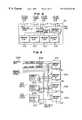
- FIG. 1shows the arrangement of a typical personal computer which is equipped with the flash memory based file memory device of this invention.
- reference numeral 1denotes a CPU which controls the implementation of programs and has a 32-bit data bus
- 2is a clock generator for generating a system clock signal.
- 3is a set of internal common signal buses including a data bus, address bus, memory command lines and I/O command lines, and these are generically called “system bus”.
- 4is a file control circuit which implements the file management and memory control for the file memory device.
- 5is a set of flash memory arrays that is the storage medium of the file memory device, with each memory chip having eight access data bits.
- the file control circuit 4 and flash memory arrays 5in unison constitute the flash memory based file memory device.
- 6is a main memory control circuit
- 7is a main memory formed of DRAM elements or the like.
- 8is a peripheral I/O bus control circuit, to which are connected peripheral I/O devices including a display control circuit 9 in connection with a display unit 10 , a communication unit 11 , and an external capacious storage unit 12 .
- the peripheral I/O control circuit 8has its own clock generator, and the peripheral I/O devices normally operate in accordance with this clock. Another peripheral I/O device that operates fast in synchronism with the CPU 1 by being connected to the internal system bus 3 directly may be included. Indicated by 13 is a clock signal supplied to all functional blocks including the CPU 1 in connection with the internal system bus 3 so that their operations are synchronized. Alternatively, a lower-frequency clock signal may be supplied to these functional blocks excluding the CPU 1 , provided that it is synchronous with the CPU clock.
- Indicated by 14is a Ready control signal produced from status signals of control circuits by a readiness control circuit 15 , and it is applied to the CPU 1 .
- 16is a control circuit for an operator's input device 17 .
- the operator's input device 17is a keyboard which is controlled by a keyboard controller (KBDC) 16 in this embodiment.
- the systemstarts up when the CPU 1 loads and runs the system program.
- the operatoruses the input device 17 to specify a program to be run and the CPU 1 loads the program into the main memory 7 and processes data accordingly while displaying results on the display unit 10 .
- the CPU 1activates the communication unit 11 to send processed data to the outside, stores processed data in the external memory unit 12 , or activates the file controller 4 to make access to files in the file memory 5 .
- the control circuitsoperate in synchronism with the clock signal 13 provided by the clock generator 2 .
- a control circuitWhen a control circuit needs to halt the CPU 1 , it issues a CPU wait request signal to the readiness control circuit 15 , which then negates the Ready signal 14 to the CPU 1 . Consequently, the CPU 1 stays in the wait state until the Ready signal 14 is restored.
- the file control circuit 4determines the time length of CPU wait state depending on the number of files accessed by the CPU 1 .
- FIG. 2showing the internal arrangement of the flash memory based file memory device.
- items indicated by 3 , 4 , 5 and 13are identical to those of FIG. 1, and the rest of items are functional blocks within the file control circuit 4 .
- Indicated by 21is a set of registers for interfacing the file control circuit with the system bus, of which 22 is a status register for setting the state of the file control-circuit 4 to be indicated to the CPU, 23 is a start sector register for setting the top access sector number, 24 is an end sector register for setting the last access sector number, 25 is a command register for setting a command code of a process specified by the CPU, and 26 is a data register used to transact data with the system bus.
- Indicated by 27is a controller which controls the whole file control circuit 4 , and it is preferably a programmable intelligent LSI element such as a one-chip microcomputer.
- 28is a memory control circuit for controlling the flash memory arrays
- 29is a data control circuit for controlling the data read/write operation of the flash memory arrays
- 30is a DMA control circuit for implementing the fast memory access based on the system clock signal.
- 31is the status signal to be sent to the readiness control circuit
- 32is a local bus of the file memory device
- 33is a signal bus of the access control signals and address to the flash memory arrays.
- the CPU 1makes access to the file memory device through the system bus 3 by following the procedure as follows. Initially, the CPU reads the status register 22 to check the access availability of the file memory. Subsequently, the CPU specifies a sector of access by setting the start sector register 23 and end sector register 24 , and sets a command code (read or write) for the access in the command code register 25 . The CPU reads the status register 22 again to check the access availability, and write data or read out data in the data register 26 .
- the controller 27reads the start sector register 23 , end sector register 24 and command code register 25 to recognize the content of access to the flash memory arrays 5 , and sets a code in the status register 22 , thereby indicating the current state to the CPU 1 .
- the DMA control circuit 30is used to implement a fast flash memory access for transacting data with the system bus 3 .
- the role of the controller 27includes the setting for the DMA control circuit and memory control circuit depending on the content of access and the initiation of the DMA operation.
- the DMA control circuit 30generates the address and timing signals necessary for the DMA operation, and the memory control circuit 28 generates the access signal in accordance with the timing signal.
- the flash memory arrays 5transact data with the data control circuit 29 in response to these signals, and the data control circuit 29 forms data depending on the number of sectors of access.
- the data coming over the system bus 3 in one access operationis reformed to have a width equal to the number of bits of writing to a flash memory chip.
- 32-bit datais sent over the 32-bit data bus of the system bus 3 and the flash memory chip has a 8-bit data width, and accordingly the transferred 32-bit data is written by being divided in four write operations to the flash memory array.
- the data control circuit 29divides the 32-bit data into four pieces of 8-bit data by using a latch circuit.
- the data control circuit 29reads a flash memory array four times and composes a piece of 32-bit data so that it is sent at once over the 32-bit data bus.
- the wait time of the system bus 3is created by a CPU wait request caused by the status signal 31 that is generated by the data control circuit 29 .
- the size of data latched by the data control circuit 29is adjusted so as to implement the fast access. For example, for a continuous read access of four sectors, four 8-bit flash memory chips are read concurrently so that 32-bit data is accessed at once. In this case, however, it is necessary for the data to have been written in the four flash memory chips concurrently so that the data is arranged uniquely for both write and read access operations, as mentioned previously.
- information processing systemsgenerally transact data with the file memory in the form of files, i.e., the number of sectors of data that is read out is equal to that of the data at the write access, and therefore no special care is needed so far as file data is written and read out in the same access mode in terms of the number of sectors.
- continuous access of file data of six sectorsis carried out as a parallel access of four sectors and a parallel access of two sectors.
- Information on the data storage mannermay be recorded for sector-wise data stored in the flash memory arrays 5 so as to ensure the consistency. This information can be recorded in the redundant data storage area except the data storage area if it is available, or otherwise recorded in another area provided separately.
- FIG. 3The figure shows the case of the system with a 32-bit system bus and a flash memory with a 8-bit data width.
- Functional blocks explained previouslyare referred to by the common symbols.
- indicated by 41is a counter which generates the address for the DMA control circuit 30 from the clock signal 13 and the I/O access command or memory access command on the system bus 3 .
- 42is a DMA start register in connection with the local bus 32 of the controller 27 , and an intended DMA transfer is started by putting a certain code in this register.
- 43is a sector register in connection with the local bus 32 , and DMA transfer for an intended sector is carried out by putting the sector number in it.
- This registeris practically used to generate the high-order address and chip select signal for the flash memory by delivering the set value of sector number to the memory control circuit 28 .
- 44is a timing control circuit for generating a timing signal used to synchronize the operations of control circuits at DMA transfer.
- 45is the memory address generated by the memory control circuit 28 from the values of the counter 41 and sector register, and 46 is a set of memory control signals produced by the memory control circuit 28 by being timed to the generation of the memory address.
- 51 , 52 , 53 and 54are 1-byte (8-bit) data latches which are combined to form a 4-byte (32-bit) data latch used for data width conversion between 32-bit data and 8-bit data within the data control circuit 29 .
- the latches 51 - 54hold D 0 -D 7 , D 8 -D 15 , D 16 -D 23 and D 24 -D 31 , respectively.
- 55is a latch signal generation circuit associated with these latches.
- 56is a data width setting register in connection with the local bus 32 , and it is used to set the data width and data arrangement mode.
- one of “1”, “2” and “4”is set as a number of sectors of continuous read access so that the timing of latch signal generation is indicated to the latch signal generation circuit 55 . Consequently, the data latches 51 - 54 receive latch signals 57 , 58 , 59 and 60 , respectively.
- the circuit 55produces the latch signals 57 - 60 sequentially to produce 32-bit data on the system bus 3 through four-time accesses to a flash memory chip.
- the circuit 55produces a latch signal pair 57 and 58 and next another latch signal pair 59 and 60 alternately to produce 32-bit data on the system bus 3 through two-time accesses to two flash memory chips for each signal pair.
- the circuit 55produces the latch signals 57 - 60 simultaneously to produce 32-bit data on the system bus 3 through a single access to four flash memory chips.
- the latch signals 57 - 60are always fed simultaneously to all data latches 51 - 54 so that 32-bit data on the system bus is latched at once.
- 61is a data distribution circuit for distributing data from the data latches to the flash memory or from the flash memory to the data latches.
- 62is a data bus between the data distribution circuit and flash memory arrays, and 63 is a read/write signal supplied from the command register 25 among the interface registers 21 , for example, for determining the data transfer direction of the data distribution circuit 61 .
- the data distribution circuit 61is a bidirectional buffer, having one I/O ports connected to the data latches 51 - 54 and another I/O ports connected to the flash memory arrays 5 .
- the I/O ports for the flash memory arrays 5are 32 bits, which are grouped into four bit groups, i.e., bit 0 through bit 7 , bit 8 through bit 15 , bit 16 through bit 23 and bit 24 through bit 31 , and each bit group is connected to one of four memory groups of the flash memory chips.
- the manner of data distributionis determined depending on the contents of the data width setting register 56 .
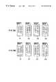
- FIG. 12The data distributing operation will be explained specifically with reference to FIG. 12, FIG. 13 and FIG. 14 .
- FIG. 12lists examples of data distribution implemented by the data distribution circuit 61 in response to the setup value of the data width setting register 56 .
- FIG. 12Listed in FIG. 12 is for one-sector continuous access
- FIG. 13is for two-sector continuous access
- FIG. 14is for four-sector continuous access, with each case including four kinds of data distribution depending on as to which of four memory groups is accessed.
- For one continuous access sectorone access operation takes four system cycles
- For two continuous access sectorone access operation takes two system cycles
- four continuous access sectorone access operation takes one system cycle.
- One-sector continuous accessfalls into four cases depending on which ever of four memory divisions, and two-sector continuous access and four-sector continuous access also fall into four cases each depending on whichever memory group is accessed at the beginning. Accordingly, the access starting memory group can be determined properly so that all memory chips are used evenly. Although fixed designation of a certain memory group as the access starting group simplifies the data distributing logics, this group will be used most frequently and ultimately will become defective, resulting in the failure of fast write access of four continuous sectors.
- the distribution circuithas different wiring among operation cycles for the read access of one or two continuous sectors, the latch signals are supplied only to relevant latches and therefore the wiring may be common to all cycles.
- the data distributioncycles from memory group 1 to latch 1 , from memory group 1 to latch 2 , from memory group 1 to latch 3 and from memory group 1 to latch 4 , but this may be altered to the wiring from memory group 1 to all latches in all cycles.
- the access controlwill be explained more specifically.
- data of bit positions among the 32-bit data bus 62 in connection with a memory groupis transferred from the data latch 51 in the first cycle, and similarly data from the data latches 52 , 53 and 54 , and again from 51 , 52 and so on are transferred to corresponding memory groups in the second cycle, third cycle and fourth cycle, and again in the first cycle, second cycle and so on, as shown in FIG. 12 .
- data from flash memory chipsare distributed into the four data latches in accordance with the latch signals in the corresponding cycles so that 32-bit data is formed.
- data of bit positions among the 32-bit data bus 62 in connection with two flash memory groupsare transferred alternately from the data latches 51 and 52 in the first cycle and from the data latches 53 and 54 in the second cycle, as shown in FIG. 13 .
- data from two pairs of memory groupsare distributed alternately to the data latches 51 and 52 in the first cycle and to 53 and 54 in the second cycle.
- the whole data on the 32-bit data bus 62is transferred at once from the data latches 51 - 54 to the memory groups in connection in one cycle.
- 32-bit data from the memory groupsis transferred to the data latches in one cycle.
- the controller 27sets the registers appropriately prior to the activation of the DMA control circuit 30 .
- FIGS. 5 A and 5 Bshow first through fourth memory groups 81 - 84 .
- FIG. 5Ashows the memory contents after some files have been stored
- FIG. 5Bshows the memory contents, with some files being revised to have increased sizes.
- Symbol m-nsignifies a file number m and a sector number n of the file, e.g., data 3 - 2 is of file number 3 and sector number 2 .
- each areahas a capacity of one sector
- the contents of sectorsare distributed to memory areas, instead of only the contents of a single sector being stored in a 1-sector area of each memory group. This affair will be explained in more detail later in connection with the file management.
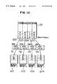
- FIG. 9An alternative scheme of giving different addresses to individual memory groups will be explained on FIG. 9 .
- the figureshows the arrangement of the address generation circuit in the memory control circuit 28 for the case of four memory groups.
- Indicated by 201 - 204are four memory groups a, b, c and d that constitute the flash memory arrays 5 .
- 205 , 206 and 207are latch circuits b, c and d for the high-order addresses given to the memory groups b, c and d, respectively.
- Indicated by 208is an address bus (corresponding to 45 in FIG. 3) of the memory control circuit 28 , and 209 is the low-order address of the address bus 208 , with the number of address bits matching the addressing to the unit erasure block of the flash memory chip or the unit area of file management.
- the low-order addressis 9 bits for a unit erasure block of 512 bytes. In case the unit erasing area of flash memory chip is smaller than the unit area of file management, the number of address bits is determined to match the file management unit area.
- 210is an high-order address portion of the address bus 208 necessary for addressing the memory group.
- Indicated by 211 , 212 and 213are high-order addresses held in the address latches b, c and d for addressing the memory groups b, c and d, respectively.
- 214 , 215 , 216 and 217are memory control signals for the memory groups a, b, c and d, respectively.
- the high-order addresses of memory groupsare set in advance in the corresponding address latch circuits 205 - 207 .
- the address busis supplied with an address for the memory group a, with its low-order address being common to all memory groups, and the memory groups b, c and d are addressed for their high-order addresses by the respective address latch circuits.
- Access controlis entirely carried out through the memory control signals 214 - 217 , and for the access to only memory groups a and b for example, only the memory control signals 214 and 215 are made active.
- the memory group amay be given any address provided that the memory control signal 214 is inactive.
- the CPU 1can have a fast read/write access to intended sectors through simple settings to a relatively small number of registers.
- a file controller formed of a one-chip microcomputerit becomes possible to implement precise control on a software basis, and based on a DMA control circuit, fast data transfer is made possible even if the one-chip microcomputer is slower than the CPU. If the one-chip microcomputer is fast enough to follow the CPU operation, it is feasible to arrange a system in which the DMA control circuit is eliminated and the one-chip microcomputer performs the entire data transfer.
- FIG. 15shows specific examples of the hardware arrangement for dealing with various combinations of system data widths and flash memory data widths.
- the tablehas columns of 4-bit, 8-bit, 16-bit and 32-bit flash memory data widths, and rows of 16-bit and 32-bit system data widths that dominate the present personal computers and 64-bit and 128-bit system data widths that are adopted by high-performance computers and will be adopted by future personal computers.
- the data distribution circuitis characterized in terms of the number of bits of data distributed by one distribution circuit times the number of distribution circuits, i.e., in the figures including the data distribution circuit 61 , each circle represents data distributed by one distribution circuit and the number of circles represents the number of distribution circuits.
- These distribution circuitsare connected as shown in FIGS. 12, 13 and 14 .
- the number of latchesis selected from 1 through 4 derived from the latches 51 - 54 of the foregoing embodiment, and in case the memory data width is greater than the system data width, the latches are placed on the part of the data distribution circuit.
- the number of memory groupsis derived from four divisions of the foregoing embodiment.
- the number of distribution ports of the data distribution circuit and the number of latches and memory groups exemplified in the foregoing embodimentare the minimum requisite.
- the systemwill have an enhanced performance if the circuit scale and terminals can afford to increase these numbers.
- Increasing the number of memory groupsexpands the latitude of selection of data storage locations, preventing the uneven use of memory cells. It also increases the number of memory locations accessed in parallel, resulting in an enhanced memory access speed.
- the speed-up of memory access based on the interleaving schemecan be accomplished through the concurrent access to multiple memory chips, although the effect of data bus matching mentioned in the foregoing embodiment is lost.
- the number of distribution ports and latchesmust be increased at the same time of increasing the number of memory groups.
- the flash memoryincludes an internal write buffer desirably, although it will become unnecessary in the future when the flash memory will have a sufficiently fast write operation.
- an independent write buffermay be placed between the data control circuit and the flash memory. At a write access, data from the system is written temporarily to the write buffer and thereafter it is written to the flash memory.
- FIG. 4shows an embodiment of this arrangement, in which functional blocks explained previously are referred to by the common-symbols.
- 71is a data selector that switches the connection of the data distribution circuit 61 depending on whether the access is for reading or writing
- 72is a write buffer with the same data bus width as the CPU bus width for holding write data temporarily
- 73is the read/write signal for operating the data selector 71 produced from the command code loaded in the command register 25 .
- the data distribution circuit 61In response to a write access, the data distribution circuit 61 is connected to the write buffer 72 so that write data from the system is held in the write buffer 72 , and thereafter it is written to the flash memory arrays 5 by the controller. In response to a read access, the data distribution circuit 61 is connected directly to the flash memory arrays 5 , and the same operation of read access explained on FIG. 3 takes place. Based on this arrangement, it becomes possible for the system to have a fast flash memory access even if a flash memory of slow write operation without a built-in write buffer is used.
- FIGS. 5A and 5Bshow the assignment of unit areas (one sector) of each memory group to sectors of files as a result of the soft ware-based file storing operation.
- four sectorse.g., 1 - 1 through 1 - 4 as shown
- These sector dataare actually stored by being distributed to four unit areas.
- Two sectorse.g., 1 - 5 and 1 - 6 as shown
- a remaining sectore.g., 1 - 7
- the distributive storing operation for two sectors and four sectorswill be explained in more detail with reference to FIG. 10 and FIG. 11 showing examples of 4-byte and 2-byte simultaneous write operations, respectively
- the systemhas a 32-bit data bus and each memory group has a 8-bit data access width as in the preceding embodiment.
- FIG. 10shows the case of 4-sector concurrent writing to four memory groups a, b, c and d.
- Indicated by 221are 32-bit (4-byte) data coming over the system bus
- 222 - 225are serial numbers of 8-bit (1-byte) data
- 222 , 223 , 224 and 225are first, second, third and fourth byte data, respectively.
- Data of the first through 2048th bytes of four sectorsare sent continuously in such a manner that the first through fourth bytes are sent concurrently at the beginning over the 32-bit bus.
- Indicated by 51 - 54are data latches shown in FIG. 3 for holding data temporarily.
- FIGS. 5A and 5Bshow the assignment of specific memory groups to individual sectors, data of each sector is actually written by being distributed to the memory groups a-d.
- 4-sector dataare stored in a 4-sector area provided by the memory groups a, b, c and d.
- FIG. 11shows 2-byte concurrent writing to the memory groups a and b.
- the latched datais divided into two parts.
- the first 2-byte datais written in the memory groups a and b, and subsequently the second 2-byte data is written additionally in the memory groups a and b.
- 512-byte data of the first sectorare written in the memory groups a and b, and subsequently 512-byte data of the second sector are written additionally in the memory groups a and b.
- the first sectoris written by being distributed to the memory groups a and b, instead of being stored in a particular memory group, and the second sector is distributed to the memory groups a and b in the same manner.
- byte data of the data latches 51 - 54are stored in a certain memory group. In this case only, the 1-sector data is stored in a particular memory group without being distributed.
- FIG. 5Ashows the memory contents after some files have been stored
- FIG. 5Bshows the memory contents, with some files being revised to have increased sizes.
- filesare initially stored closely in the ascending order of the file number, with a memory group being assigned to each sector number sequentially and cyclically.
- file sectorsare stored such that the assigned memory groups are continuous.
- a file with file number 4 made up of five sectors 4 - 1 through 4 - 5is initially stored as shown in FIG. 5A, and the file has additional two sectors 4 - 6 and 4 - 7 in FIG. 5 B. Since the file starts with its top sector 4 - 1 at the memory group 3 , the additional sectors 4 - 6 and 4 - 7 have their areas reserved in the memory groups 2 and 3 .
- the sectors 4 - 5 and 4 - 6are treated as two continuous sectors and the sector 4 - 7 is treated as a single sector. Namely, additional sectors are treated to be continuous to the existing sectors.
- the file management systemmay be designed such that the system specifies access sectors by setting a starting sector and the number of sectors on a hardware basis, and the file system controls their physical storage locations.
- the end sector register 24 shown in FIG. 2is unnecessary.
- Information for chaining file sectorsis stored in a redundant area of the memory, if it exists, or otherwise in a separate memory means so that once the file starting sector number is specified, physical storage locations of the successive sectors can be traced for the continuous sector access.
- FIG. 6shows an example of the chaining information.
- Indicated by 85is stored file data having file number 4 and sector number 5 .
- 86is file data of the next sector having file number 4 and sector number 6
- 87is file data of the next sector having file number 4 and sector number 7 .
- the data sectors of this examplehave sequential sector numbers, data may be stored by being scrambled through the concurrent access to multiple memory chips. Even in such a case, the sector number has a crucial role for storing byte-wise data in order.
- Indicated by 88is the physical address of the file data 85 , with its left-hand numeral “ 3 ” indicating the memory group number and its right-hand numeral “ 5 ” indicating the address within the memory group.
- 89 and 90are physical addresses of the stored file data 86 and 87 .
- 91is chaining information that points the physical address of the next sector of the file data 85 , i.e., the physical address of the file data 86 in this case, with its left-hand numeral indicating the memory group number and its right-hand numeral indicating the address within the memory group.
- chaining information 92indicates the physical address of the file data 87 .
- Chaining information 93has its content indicating the absence of a successive sector, i.e., this is the last sector of the file of file number 4 .
- the CPU of the systemdoes not need to recognize the physical location of a file in order to access to it, but the file controller makes reference to the chaining information to reach the physical location in the memory. Consequently, it becomes possible to make a continuous access to a file even if it is not stored in continuous locations.
- the file controllermakes reference to the chaining information to reach the physical location in the memory. Consequently, it becomes possible to make a continuous access to a file even if it is not stored in continuous locations.
- means of entering multiple addresses for the concurrent access to multiple memory groupsis necessary.
- low-order address for 1-sector accessis used commonly, as explained on FIG. 9, and therefore it is required only for the high-order address portion.
- addressing of files from the systemis simplified, and it can be carried out by dealing with a small amount of information.
- FIG. 7shows the arrangement of a memory element including multiple memory chips and associated circuitry packaged in a single case.
- 101is a memory element
- 102 - 105are memory chips of the same structure
- 106 - 109are input/output data terminals of the element each used for the data input/output of one memory chip.
- the memory elementhas 32-bit data input/output terminals consisting of the four 8-bit data input/output terminals 106 - 109 .
- 110is an input terminal of a signal 111 that is provided by the user for specifying the connection between the memory chips and data input/output terminals
- 112is a data connection circuit.
- the data connectionis selected based on the data distribution in the data control circuit explained previously on FIG. 12 through FIG. 14, for example.
- the received connection setting signal 111is fed to the data connection circuit 112 , which then connects the memory chips 102 - 105 to the data input/output terminals 106 - 109 accordingly so that data is transferred between the memory chips and the external data bus.
- FIG. 8shows the arrangement of a memory element which is designed to set the data connection between the memory chips and input/output terminals based on the command entered by the user.
- a command control circuitincluding a command setting register for producing the data connection setting signal 111 based on the setup value
- 114is a set of data lines for feeding a command value, which is received on a data input/output terminal, to the command control circuit 113 .
- Remaining portions of the arrangementare identical to FIG. 7 .
- the userselects an internal data connection by making reference to FIG. 12 through FIG. 14, and enters the respective command code to the command control circuit 113 through the data lines 114 .
- the command control circuit 113produces a data connection setting signal 111 in accordance with the command code and applies it to the data connection circuit 112 .
- the subsequent operationis identical to the arrangement of FIG. 7 .
- memory elements based on these embodiments explained on FIG. 7 and FIG. 8are effective for the simplification of the peripheral circuitry of the file memory device.
- memory chips and associated control circuitsare packaged in a memory package, integrating these components within a single chip will further enhance the compactness and fast memory access performance.
Landscapes
- Engineering & Computer Science (AREA)
- Theoretical Computer Science (AREA)
- Physics & Mathematics (AREA)
- General Engineering & Computer Science (AREA)
- General Physics & Mathematics (AREA)
- Human Computer Interaction (AREA)
- Information Retrieval, Db Structures And Fs Structures Therefor (AREA)
- Read Only Memory (AREA)
- Memory System (AREA)
Abstract
Description
Claims (29)
Priority Applications (3)
| Application Number | Priority Date | Filing Date | Title |
|---|---|---|---|
| US09/793,967US6351787B2 (en) | 1993-03-11 | 2001-02-28 | File memory device and information processing apparatus using the same |
| US10/023,701US6662264B2 (en) | 1993-03-11 | 2001-12-21 | File memory device and information processing apparatus using the same |
| US10/683,066US6952752B2 (en) | 1993-03-11 | 2003-10-14 | File memory device and information processing apparatus using the same |
Applications Claiming Priority (2)
| Application Number | Priority Date | Filing Date | Title |
|---|---|---|---|
| JP5051041AJPH06266596A (en) | 1993-03-11 | 1993-03-11 | Flash memory file storage device and information processor |
| JP5-051041 | 1993-03-11 |
Related Child Applications (1)
| Application Number | Title | Priority Date | Filing Date |
|---|---|---|---|
| US09/793,967ContinuationUS6351787B2 (en) | 1993-03-11 | 2001-02-28 | File memory device and information processing apparatus using the same |
Publications (1)
| Publication Number | Publication Date |
|---|---|
| US6272610B1true US6272610B1 (en) | 2001-08-07 |
Family
ID=12875722
Family Applications (4)
| Application Number | Title | Priority Date | Filing Date |
|---|---|---|---|
| US08/207,749Expired - LifetimeUS6272610B1 (en) | 1993-03-11 | 1994-03-09 | File memory device using flash memories, and an information processing system using the same |
| US09/793,967Expired - Fee RelatedUS6351787B2 (en) | 1993-03-11 | 2001-02-28 | File memory device and information processing apparatus using the same |
| US10/023,701Expired - Fee RelatedUS6662264B2 (en) | 1993-03-11 | 2001-12-21 | File memory device and information processing apparatus using the same |
| US10/683,066Expired - Fee RelatedUS6952752B2 (en) | 1993-03-11 | 2003-10-14 | File memory device and information processing apparatus using the same |
Family Applications After (3)
| Application Number | Title | Priority Date | Filing Date |
|---|---|---|---|
| US09/793,967Expired - Fee RelatedUS6351787B2 (en) | 1993-03-11 | 2001-02-28 | File memory device and information processing apparatus using the same |
| US10/023,701Expired - Fee RelatedUS6662264B2 (en) | 1993-03-11 | 2001-12-21 | File memory device and information processing apparatus using the same |
| US10/683,066Expired - Fee RelatedUS6952752B2 (en) | 1993-03-11 | 2003-10-14 | File memory device and information processing apparatus using the same |
Country Status (3)
| Country | Link |
|---|---|
| US (4) | US6272610B1 (en) |
| JP (1) | JPH06266596A (en) |
| KR (1) | KR960016397B1 (en) |
Cited By (48)
| Publication number | Priority date | Publication date | Assignee | Title |
|---|---|---|---|---|
| US6397314B1 (en)* | 1995-07-31 | 2002-05-28 | Lexar Media, Inc. | Increasing the memory performance of flash memory devices by writing sectors simultaneously to multiple flash memory devices |
| US6578127B1 (en)* | 1996-04-02 | 2003-06-10 | Lexar Media, Inc. | Memory devices |
| US20040024957A1 (en)* | 2001-08-07 | 2004-02-05 | Chun-Hung Lin | Window-based flash memory storage system and management and access methods thereof |
| US6735661B2 (en)* | 2000-06-27 | 2004-05-11 | Koninklijke Philips Electronics N.V. | Integrated circuit with flash memory including dedicated flash bus and flash bridge |
| US6757800B1 (en)* | 1995-07-31 | 2004-06-29 | Lexar Media, Inc. | Increasing the memory performance of flash memory devices by writing sectors simultaneously to multiple flash memory devices |
| US20050141313A1 (en)* | 2003-12-30 | 2005-06-30 | Gorobets Sergey A. | Non-volatile memory and method with memory planes alignment |
| US20050144367A1 (en)* | 2003-12-30 | 2005-06-30 | Sinclair Alan W. | Data run programming |
| US20050144357A1 (en)* | 2003-12-30 | 2005-06-30 | Sinclair Alan W. | Adaptive metablocks |
| US20050144363A1 (en)* | 2003-12-30 | 2005-06-30 | Sinclair Alan W. | Data boundary management |
| US6950918B1 (en) | 2002-01-18 | 2005-09-27 | Lexar Media, Inc. | File management of one-time-programmable nonvolatile memory devices |
| US6957295B1 (en) | 2002-01-18 | 2005-10-18 | Lexar Media, Inc. | File management of one-time-programmable nonvolatile memory devices |
| US6973519B1 (en) | 2003-06-03 | 2005-12-06 | Lexar Media, Inc. | Card identification compatibility |
| US6978342B1 (en) | 1995-07-31 | 2005-12-20 | Lexar Media, Inc. | Moving sectors within a block of information in a flash memory mass storage architecture |
| US20050286855A1 (en)* | 2003-04-25 | 2005-12-29 | Matsushita Electric Industrial Co., Ltd. | Data recording apparatus |
| US7000064B2 (en) | 2001-09-28 | 2006-02-14 | Lexar Media, Inc. | Data handling system |
| US20060067181A1 (en)* | 1999-05-08 | 2006-03-30 | Samsung Electronics Co., Ltd | Recording medium for storing linking type information and method of processing defective area using the same |
| US20060136668A1 (en)* | 2004-12-17 | 2006-06-22 | Rudelic John C | Allocating code objects between faster and slower memories |
| US20060190983A1 (en)* | 2001-12-05 | 2006-08-24 | Plourde Harold J Jr | Disk driver cluster management of time shift buffer with file allocation table structure |
| US7102671B1 (en) | 2000-02-08 | 2006-09-05 | Lexar Media, Inc. | Enhanced compact flash memory card |
| US7111140B2 (en) | 1995-07-31 | 2006-09-19 | Lexar Media, Inc. | Increasing the memory performance of flash memory devices by writing sectors simultaneously to multiple flash memory devices |
| US20060209196A1 (en)* | 2003-03-12 | 2006-09-21 | Takeshi Ohtsuka | Camera recorder and data recording medium |
| US20060256624A1 (en)* | 2003-06-24 | 2006-11-16 | Micron Technology, Inc. | Erase block data splitting |
| US7167944B1 (en) | 2000-07-21 | 2007-01-23 | Lexar Media, Inc. | Block management for mass storage |
| US7185208B2 (en) | 2001-09-28 | 2007-02-27 | Lexar Media, Inc. | Data processing |
| US20070055821A1 (en)* | 2003-11-28 | 2007-03-08 | Takeshi Ootsuka | Recording apparatus |
| EP0923023A4 (en)* | 1997-04-16 | 2007-04-25 | Sony Corp | Recording medium control device and method |
| US20070101095A1 (en)* | 2005-10-27 | 2007-05-03 | Sandisk Corporation | Methods for adaptively handling data writes in non-volatile memories |
| US7215580B2 (en) | 2001-09-28 | 2007-05-08 | Lexar Media, Inc. | Non-volatile memory control |
| US7231643B1 (en) | 2002-02-22 | 2007-06-12 | Lexar Media, Inc. | Image rescue system including direct communication between an application program and a device driver |
| US7254724B2 (en) | 2001-09-28 | 2007-08-07 | Lexar Media, Inc. | Power management system |
| US7275686B2 (en) | 2003-12-17 | 2007-10-02 | Lexar Media, Inc. | Electronic equipment point-of-sale activation to avoid theft |
| US7340581B2 (en) | 2001-09-28 | 2008-03-04 | Lexar Media, Inc. | Method of writing data to non-volatile memory |
| US7370166B1 (en) | 2004-04-30 | 2008-05-06 | Lexar Media, Inc. | Secure portable storage device |
| US7464306B1 (en) | 2004-08-27 | 2008-12-09 | Lexar Media, Inc. | Status of overall health of nonvolatile memory |
| US7523249B1 (en) | 1995-07-31 | 2009-04-21 | Lexar Media, Inc. | Direct logical block addressing flash memory mass storage architecture |
| WO2009107426A1 (en)* | 2008-02-29 | 2009-09-03 | Kabushiki Kaisha Toshiba | Memory system |
| US7594063B1 (en) | 2004-08-27 | 2009-09-22 | Lexar Media, Inc. | Storage capacity status |
| US7631162B2 (en) | 2005-10-27 | 2009-12-08 | Sandisck Corporation | Non-volatile memory with adaptive handling of data writes |
| US7725628B1 (en) | 2004-04-20 | 2010-05-25 | Lexar Media, Inc. | Direct secondary device interface by a host |
| US20100146196A1 (en)* | 2001-02-27 | 2010-06-10 | Fujitsu Microelectronics Limited | Memory system having a plurality of types of memory chips and a memory controller for controlling the memory chips |
| US7917709B2 (en) | 2001-09-28 | 2011-03-29 | Lexar Media, Inc. | Memory system for data storage and retrieval |
| CN102354299A (en)* | 2004-02-04 | 2012-02-15 | 株式会社东芝 | Memory card and semiconductor device |
| US8171203B2 (en) | 1995-07-31 | 2012-05-01 | Micron Technology, Inc. | Faster write operations to nonvolatile memory using FSInfo sector manipulation |
| US9319733B2 (en) | 2001-12-06 | 2016-04-19 | Cisco Technology, Inc. | Management of buffer capacity for video recording and time shift operations |
| US9817593B1 (en) | 2016-07-11 | 2017-11-14 | Sandisk Technologies Llc | Block management in non-volatile memory system with non-blocking control sync system |
| US10114562B2 (en) | 2014-09-16 | 2018-10-30 | Sandisk Technologies Llc | Adaptive block allocation in nonvolatile memory |
| US10412439B2 (en) | 2002-09-24 | 2019-09-10 | Thomson Licensing | PVR channel and PVR IPG information |
| US20220114147A1 (en)* | 2018-12-19 | 2022-04-14 | Sony Group Corporation | Information processing apparatus, information processing method, and information processing program |
Families Citing this family (35)
| Publication number | Priority date | Publication date | Assignee | Title |
|---|---|---|---|---|
| JP3718578B2 (en)* | 1997-06-25 | 2005-11-24 | ソニー株式会社 | Memory management method and memory management device |
| US6708257B2 (en)* | 1999-07-12 | 2004-03-16 | Koninklijke Philips Electronics N.V. | Buffering system bus for external-memory access |
| US7671295B2 (en) | 2000-01-10 | 2010-03-02 | Electro Scientific Industries, Inc. | Processing a memory link with a set of at least two laser pulses |
| JP4609680B2 (en)* | 2000-08-09 | 2011-01-12 | ソニー株式会社 | Data storage device |
| US20040049627A1 (en)* | 2001-11-09 | 2004-03-11 | Flex-P Industries | Method and system for controlling compact flash memory |
| KR100445915B1 (en)* | 2002-01-22 | 2004-08-25 | 한국전자통신연구원 | Apparatus for controlling memory system |
| US7454603B2 (en)* | 2002-02-11 | 2008-11-18 | Intel Corporation | Method and system for linking firmware modules in a pre-memory execution environment |
| US20030204675A1 (en)* | 2002-04-29 | 2003-10-30 | Dover Lance W. | Method and system to retrieve information from a storage device |
| US7515598B2 (en)* | 2002-10-29 | 2009-04-07 | Intel Corporation | Configurable transmit and receive system interfaces for a network device |
| KR100560761B1 (en)* | 2003-07-08 | 2006-03-13 | 삼성전자주식회사 | Interface conversion system and method |
| US7631138B2 (en) | 2003-12-30 | 2009-12-08 | Sandisk Corporation | Adaptive mode switching of flash memory address mapping based on host usage characteristics |
| US8504798B2 (en)* | 2003-12-30 | 2013-08-06 | Sandisk Technologies Inc. | Management of non-volatile memory systems having large erase blocks |
| US9104315B2 (en) | 2005-02-04 | 2015-08-11 | Sandisk Technologies Inc. | Systems and methods for a mass data storage system having a file-based interface to a host and a non-file-based interface to secondary storage |
| US7516252B2 (en)* | 2005-06-08 | 2009-04-07 | Intel Corporation | Port binding scheme to create virtual host bus adapter in a virtualized multi-operating system platform environment |
| JP4969811B2 (en)* | 2005-07-22 | 2012-07-04 | 株式会社東芝 | Information processing system and memory control device |
| US7765350B2 (en)* | 2005-09-14 | 2010-07-27 | Koninklijke Philips Electronics N.V. | Method and system for bus arbitration |
| ATE488009T1 (en)* | 2006-03-31 | 2010-11-15 | Mosaid Technologies Inc | FLASH MEMORY SYSTEM CONTROL METHOD |
| US7769942B2 (en)* | 2006-07-27 | 2010-08-03 | Rambus, Inc. | Cross-threaded memory system |
| KR100921748B1 (en)* | 2007-06-04 | 2009-10-15 | 삼성전자주식회사 | Memory system including ECC circuit and driving method thereof |
| US20090113116A1 (en)* | 2007-10-30 | 2009-04-30 | Thompson E Earle | Digital content kiosk and methods for use therewith |
| ITMI20082331A1 (en)* | 2008-12-29 | 2010-06-30 | Giovanni Lucchetta | SOLID STATE DISC, PARTICULARLY FOR THE STORAGE OF DIGITAL DATA. |
| US8495471B2 (en)* | 2009-11-30 | 2013-07-23 | International Business Machines Corporation | Solid-state storage system with parallel access of multiple flash/PCM devices |
| US8533407B2 (en)* | 2010-12-01 | 2013-09-10 | International Business Machines Corporation | Capacity management in deduplication storage systems |
| CN102306124A (en)* | 2011-08-01 | 2012-01-04 | 深圳市文鼎创数据科技有限公司 | Method for implementing hardware driver layer of Nand Flash chip |
| JP5914148B2 (en)* | 2012-05-07 | 2016-05-11 | 株式会社バッファローメモリ | SSD (solid state drive) device |
| KR102024850B1 (en)* | 2012-08-08 | 2019-11-05 | 삼성전자주식회사 | Memory system including three dimensional nonvolatile memory device and programming method thereof |
| CN102981965A (en)* | 2012-11-07 | 2013-03-20 | 江苏乐买到网络科技有限公司 | NAND FLASH file system |
| US9563363B2 (en)* | 2013-09-27 | 2017-02-07 | Empire Technology Development Llc | Flexible storage block for a solid state drive (SSD)-based file system |
| JP6467636B2 (en)* | 2014-08-28 | 2019-02-13 | パナソニックIpマネジメント株式会社 | Memory card |
| CN104717557B (en)* | 2014-11-25 | 2018-09-14 | 四川长虹电器股份有限公司 | A method of Flash data is read based on set-top box |
| CN104615546B (en)* | 2015-02-13 | 2018-04-27 | 小米科技有限责任公司 | file data management method and device |
| TWI562154B (en)* | 2015-02-17 | 2016-12-11 | Silicon Motion Inc | Methods for reading data from a storage unit of a flash memory and apparatuses using the same |
| KR102299880B1 (en)* | 2017-04-04 | 2021-09-09 | 에스케이하이닉스 주식회사 | Data conversion apparatus and method |
| US11521690B2 (en)* | 2018-03-16 | 2022-12-06 | Micron Technology, Inc. | NAND data placement schema |
| CN112074816B (en) | 2018-03-16 | 2025-02-21 | 美光科技公司 | Cluster parity for NAND data placement patterns |
Citations (9)
| Publication number | Priority date | Publication date | Assignee | Title |
|---|---|---|---|---|
| US3753235A (en)* | 1971-08-18 | 1973-08-14 | Ibm | Monolithic memory module redundancy scheme using prewired substrates |
| US4051354A (en)* | 1975-07-03 | 1977-09-27 | Texas Instruments Incorporated | Fault-tolerant cell addressable array |
| US4483001A (en)* | 1982-06-16 | 1984-11-13 | International Business Machines Corporation | Online realignment of memory faults |
| JPS6161A (en) | 1984-06-08 | 1986-01-06 | Ube Ind Ltd | Method for producing 4,4'-azobis(4-cyanovaleric acid) |
| JPS62217496A (en) | 1986-03-18 | 1987-09-24 | Fujitsu Ltd | EEPROM writing method |
| US4903239A (en)* | 1987-03-30 | 1990-02-20 | Nec Corporation | Semiconductor memory having a parallel input/output circuit |
| JPH02297798A (en) | 1989-05-12 | 1990-12-10 | Sony Corp | Differential amplifier |
| US5212666A (en)* | 1989-07-10 | 1993-05-18 | Seiko Epson Corporation | Memory apparatus having flexibly designed memory capacity |
| US5263003A (en)* | 1991-11-12 | 1993-11-16 | Allen-Bradley Company, Inc. | Flash memory circuit and method of operation |
Family Cites Families (23)
| Publication number | Priority date | Publication date | Assignee | Title |
|---|---|---|---|---|
| US4162536A (en)* | 1976-01-02 | 1979-07-24 | Gould Inc., Modicon Div. | Digital input/output system and method |
| US4648064A (en)* | 1976-01-02 | 1987-03-03 | Morley Richard E | Parallel process controller |
| JPS5488242A (en) | 1977-12-21 | 1979-07-13 | Kyowa Hakko Kogyo Co Ltd | Novel derivative of fortimicin b and its preparation |
| US4310248A (en) | 1980-04-24 | 1982-01-12 | Meredith Nolan J | Color control system |
| JPS61245255A (en) | 1985-04-23 | 1986-10-31 | Hitachi Ltd | Nonvolatile memory device |
| JPS63296063A (en) | 1987-05-28 | 1988-12-02 | Canon Inc | Image forming device |
| US4961094A (en) | 1987-06-03 | 1990-10-02 | Sanyo Electric Co., Ltd. | Electrostatic recording apparatus and method for producing color images |
| US5066979A (en) | 1989-01-13 | 1991-11-19 | Canon Kabushiki Kaisha | Color image forming apparatus wherein plural colors can be formed through one printing cycle |
| EP0935255A2 (en) | 1989-04-13 | 1999-08-11 | SanDisk Corporation | Flash EEPROM system |
| US5030996A (en) | 1989-08-31 | 1991-07-09 | Canon Kabushiki Kaisha | Image forming apparatus with AC bias voltages for preventing developer mixture |
| US5167024A (en)* | 1989-09-08 | 1992-11-24 | Apple Computer, Inc. | Power management for a laptop computer with slow and sleep modes |
| JPH087475B2 (en) | 1990-01-29 | 1996-01-29 | 富士ゼロックス株式会社 | Color image forming apparatus and method of using the same |
| JPH0457295A (en) | 1990-06-22 | 1992-02-25 | Nec Corp | Electrically writable/erasable memory circuit |
| JPH0484216A (en) | 1990-07-26 | 1992-03-17 | Toshiba Corp | Data erasing method for semiconductor disk device |
| GB2251324B (en)* | 1990-12-31 | 1995-05-10 | Intel Corp | File structure for a non-volatile semiconductor memory |
| JP2979352B2 (en) | 1991-05-30 | 1999-11-15 | コニカ株式会社 | Image forming method |
| US5365325A (en) | 1992-08-10 | 1994-11-15 | Hitachi, Ltd. | Method of multi-color recording using electro-photography process and apparatus therefor wherein mixed colors generation is prevented |
| US5487133A (en)* | 1993-07-01 | 1996-01-23 | Intel Corporation | Distance calculating neural network classifier chip and system |
| US5828862A (en)* | 1994-05-04 | 1998-10-27 | International Business Machines Corporation | Game programming flash memory cartridge system including a programmer and a reprogrammable cartridge |
| US5613061A (en)* | 1994-09-12 | 1997-03-18 | Verilink Corporation | Network controller with reconfigurable program logic circuits capable of performing both channel service and testing functions |
| EP0807894A1 (en)* | 1995-01-31 | 1997-11-19 | Hitachi, Ltd. | Terminal for distributing electronic information |
| US5812755A (en)* | 1995-09-01 | 1998-09-22 | Adaptec, Incorporated | Logical and physical zones for management of defects in a headerless disk drive architecture |
| US5687114A (en)* | 1995-10-06 | 1997-11-11 | Agate Semiconductor, Inc. | Integrated circuit for storage and retrieval of multiple digital bits per nonvolatile memory cell |
- 1993
- 1993-03-11JPJP5051041Apatent/JPH06266596A/enactivePending
- 1994
- 1994-03-08KRKR1019940004411Apatent/KR960016397B1/ennot_activeExpired - Lifetime
- 1994-03-09USUS08/207,749patent/US6272610B1/ennot_activeExpired - Lifetime
- 2001
- 2001-02-28USUS09/793,967patent/US6351787B2/ennot_activeExpired - Fee Related
- 2001-12-21USUS10/023,701patent/US6662264B2/ennot_activeExpired - Fee Related
- 2003
- 2003-10-14USUS10/683,066patent/US6952752B2/ennot_activeExpired - Fee Related
Patent Citations (9)
| Publication number | Priority date | Publication date | Assignee | Title |
|---|---|---|---|---|
| US3753235A (en)* | 1971-08-18 | 1973-08-14 | Ibm | Monolithic memory module redundancy scheme using prewired substrates |
| US4051354A (en)* | 1975-07-03 | 1977-09-27 | Texas Instruments Incorporated | Fault-tolerant cell addressable array |
| US4483001A (en)* | 1982-06-16 | 1984-11-13 | International Business Machines Corporation | Online realignment of memory faults |
| JPS6161A (en) | 1984-06-08 | 1986-01-06 | Ube Ind Ltd | Method for producing 4,4'-azobis(4-cyanovaleric acid) |
| JPS62217496A (en) | 1986-03-18 | 1987-09-24 | Fujitsu Ltd | EEPROM writing method |
| US4903239A (en)* | 1987-03-30 | 1990-02-20 | Nec Corporation | Semiconductor memory having a parallel input/output circuit |
| JPH02297798A (en) | 1989-05-12 | 1990-12-10 | Sony Corp | Differential amplifier |
| US5212666A (en)* | 1989-07-10 | 1993-05-18 | Seiko Epson Corporation | Memory apparatus having flexibly designed memory capacity |
| US5263003A (en)* | 1991-11-12 | 1993-11-16 | Allen-Bradley Company, Inc. | Flash memory circuit and method of operation |
Cited By (119)
| Publication number | Priority date | Publication date | Assignee | Title |
|---|---|---|---|---|
| US20070266201A1 (en)* | 1995-07-31 | 2007-11-15 | Petro Estakhri | Increasing the memory performance of flash memory devices by writing sectors simultaneously to multiple flash memory devices |
| US8554985B2 (en) | 1995-07-31 | 2013-10-08 | Micron Technology, Inc. | Memory block identified by group of logical block addresses, storage device with movable sectors, and methods |
| US7523249B1 (en) | 1995-07-31 | 2009-04-21 | Lexar Media, Inc. | Direct logical block addressing flash memory mass storage architecture |
| US7774576B2 (en) | 1995-07-31 | 2010-08-10 | Lexar Media, Inc. | Direct logical block addressing flash memory mass storage architecture |
| US6757800B1 (en)* | 1995-07-31 | 2004-06-29 | Lexar Media, Inc. | Increasing the memory performance of flash memory devices by writing sectors simultaneously to multiple flash memory devices |
| US7441090B2 (en) | 1995-07-31 | 2008-10-21 | Lexar Media, Inc. | System and method for updating data sectors in a non-volatile memory using logical block addressing |
| US7908426B2 (en) | 1995-07-31 | 2011-03-15 | Lexar Media, Inc. | Moving sectors within a block of information in a flash memory mass storage architecture |
| US7424593B2 (en) | 1995-07-31 | 2008-09-09 | Micron Technology, Inc. | Increasing the memory performance of flash memory devices by writing sectors simultaneously to multiple flash memory devices |
| US9026721B2 (en) | 1995-07-31 | 2015-05-05 | Micron Technology, Inc. | Managing defective areas of memory |
| US8793430B2 (en) | 1995-07-31 | 2014-07-29 | Micron Technology, Inc. | Electronic system having memory with a physical block having a sector storing data and indicating a move status of another sector of the physical block |
| US8171203B2 (en) | 1995-07-31 | 2012-05-01 | Micron Technology, Inc. | Faster write operations to nonvolatile memory using FSInfo sector manipulation |
| US8397019B2 (en) | 1995-07-31 | 2013-03-12 | Micron Technology, Inc. | Memory for accessing multiple sectors of information substantially concurrently |
| US7111140B2 (en) | 1995-07-31 | 2006-09-19 | Lexar Media, Inc. | Increasing the memory performance of flash memory devices by writing sectors simultaneously to multiple flash memory devices |
| US7549013B2 (en) | 1995-07-31 | 2009-06-16 | Lexar Media, Inc. | Increasing the memory performance of flash memory devices by writing sectors simultaneously to multiple flash memory devices |
| US7263591B2 (en) | 1995-07-31 | 2007-08-28 | Lexar Media, Inc. | Increasing the memory performance of flash memory devices by writing sectors simultaneously to multiple flash memory devices |
| US8032694B2 (en) | 1995-07-31 | 2011-10-04 | Micron Technology, Inc. | Direct logical block addressing flash memory mass storage architecture |
| US8078797B2 (en) | 1995-07-31 | 2011-12-13 | Micron Technology, Inc. | Increasing the memory performance of flash memory devices by writing sectors simultaneously to multiple flash memory devices |
| US6978342B1 (en) | 1995-07-31 | 2005-12-20 | Lexar Media, Inc. | Moving sectors within a block of information in a flash memory mass storage architecture |
| US6397314B1 (en)* | 1995-07-31 | 2002-05-28 | Lexar Media, Inc. | Increasing the memory performance of flash memory devices by writing sectors simultaneously to multiple flash memory devices |
| US6578127B1 (en)* | 1996-04-02 | 2003-06-10 | Lexar Media, Inc. | Memory devices |
| EP0923023A4 (en)* | 1997-04-16 | 2007-04-25 | Sony Corp | Recording medium control device and method |
| EP0983550A4 (en)* | 1998-02-25 | 2005-09-21 | Lexar Media Inc | Increasing memory performance in flash memory devices by performing simultaneous write operation to multiple devices |
| US20060067181A1 (en)* | 1999-05-08 | 2006-03-30 | Samsung Electronics Co., Ltd | Recording medium for storing linking type information and method of processing defective area using the same |
| US7102671B1 (en) | 2000-02-08 | 2006-09-05 | Lexar Media, Inc. | Enhanced compact flash memory card |
| US6735661B2 (en)* | 2000-06-27 | 2004-05-11 | Koninklijke Philips Electronics N.V. | Integrated circuit with flash memory including dedicated flash bus and flash bridge |
| US8019932B2 (en) | 2000-07-21 | 2011-09-13 | Micron Technology, Inc. | Block management for mass storage |
| US8250294B2 (en) | 2000-07-21 | 2012-08-21 | Micron Technology, Inc. | Block management for mass storage |
| US7734862B2 (en) | 2000-07-21 | 2010-06-08 | Lexar Media, Inc. | Block management for mass storage |
| US7167944B1 (en) | 2000-07-21 | 2007-01-23 | Lexar Media, Inc. | Block management for mass storage |
| US20100146196A1 (en)* | 2001-02-27 | 2010-06-10 | Fujitsu Microelectronics Limited | Memory system having a plurality of types of memory chips and a memory controller for controlling the memory chips |
| US8312240B2 (en)* | 2001-02-27 | 2012-11-13 | Fujitsu Semiconductor Limited | Memory system having a plurality of types of memory chips and a memory controller for controlling the memory chips |
| US20040024957A1 (en)* | 2001-08-07 | 2004-02-05 | Chun-Hung Lin | Window-based flash memory storage system and management and access methods thereof |
| US7117332B2 (en)* | 2001-08-07 | 2006-10-03 | Solid State System Co., Ltd. | Window-based flash memory storage system and management and access methods thereof |
| US9489301B2 (en) | 2001-09-28 | 2016-11-08 | Micron Technology, Inc. | Memory systems |
| US9032134B2 (en) | 2001-09-28 | 2015-05-12 | Micron Technology, Inc. | Methods of operating a memory system that include outputting a data pattern from a sector allocation table to a host if a logical sector is indicated as being erased |
| US8208322B2 (en) | 2001-09-28 | 2012-06-26 | Micron Technology, Inc. | Non-volatile memory control |
| US7681057B2 (en) | 2001-09-28 | 2010-03-16 | Lexar Media, Inc. | Power management of non-volatile memory systems |
| US7254724B2 (en) | 2001-09-28 | 2007-08-07 | Lexar Media, Inc. | Power management system |
| US7000064B2 (en) | 2001-09-28 | 2006-02-14 | Lexar Media, Inc. | Data handling system |
| US8386695B2 (en) | 2001-09-28 | 2013-02-26 | Micron Technology, Inc. | Methods and apparatus for writing data to non-volatile memory |
| US8694722B2 (en) | 2001-09-28 | 2014-04-08 | Micron Technology, Inc. | Memory systems |
| US7340581B2 (en) | 2001-09-28 | 2008-03-04 | Lexar Media, Inc. | Method of writing data to non-volatile memory |
| US7944762B2 (en) | 2001-09-28 | 2011-05-17 | Micron Technology, Inc. | Non-volatile memory control |
| US7917709B2 (en) | 2001-09-28 | 2011-03-29 | Lexar Media, Inc. | Memory system for data storage and retrieval |
| US7215580B2 (en) | 2001-09-28 | 2007-05-08 | Lexar Media, Inc. | Non-volatile memory control |
| US7185208B2 (en) | 2001-09-28 | 2007-02-27 | Lexar Media, Inc. | Data processing |
| US8135925B2 (en) | 2001-09-28 | 2012-03-13 | Micron Technology, Inc. | Methods of operating a memory system |
| US7779181B2 (en)* | 2001-12-05 | 2010-08-17 | Scientific-Atlanta, Llc | Disk driver cluster management of time shift buffer with file allocation table structure |
| US20060190983A1 (en)* | 2001-12-05 | 2006-08-24 | Plourde Harold J Jr | Disk driver cluster management of time shift buffer with file allocation table structure |
| US7769925B2 (en)* | 2001-12-05 | 2010-08-03 | Scientific-Atlanta LLC | Disk driver cluster management of time shift buffer with file allocation table structure |
| US20070168601A1 (en)* | 2001-12-05 | 2007-07-19 | Plourde Harold J Jr | Disk driver cluster management of time shift buffer with file allocation table structure |
| US9319733B2 (en) | 2001-12-06 | 2016-04-19 | Cisco Technology, Inc. | Management of buffer capacity for video recording and time shift operations |
| US6950918B1 (en) | 2002-01-18 | 2005-09-27 | Lexar Media, Inc. | File management of one-time-programmable nonvolatile memory devices |
| US6957295B1 (en) | 2002-01-18 | 2005-10-18 | Lexar Media, Inc. | File management of one-time-programmable nonvolatile memory devices |
| US8166488B2 (en) | 2002-02-22 | 2012-04-24 | Micron Technology, Inc. | Methods of directly accessing a mass storage data device |
| US7231643B1 (en) | 2002-02-22 | 2007-06-12 | Lexar Media, Inc. | Image rescue system including direct communication between an application program and a device driver |
| US9213606B2 (en) | 2002-02-22 | 2015-12-15 | Micron Technology, Inc. | Image rescue |
| US10412439B2 (en) | 2002-09-24 | 2019-09-10 | Thomson Licensing | PVR channel and PVR IPG information |
| US20060209196A1 (en)* | 2003-03-12 | 2006-09-21 | Takeshi Ohtsuka | Camera recorder and data recording medium |
| EP1605694A4 (en)* | 2003-03-12 | 2010-06-09 | Panasonic Corp | CAMCORDER AND DATA RECORDING MEDIUM |
| US20050286855A1 (en)* | 2003-04-25 | 2005-12-29 | Matsushita Electric Industrial Co., Ltd. | Data recording apparatus |
| US6973519B1 (en) | 2003-06-03 | 2005-12-06 | Lexar Media, Inc. | Card identification compatibility |
| US8792277B2 (en) | 2003-06-24 | 2014-07-29 | Micron Technology, Inc. | Split data error correction code circuits |
| US8537614B2 (en) | 2003-06-24 | 2013-09-17 | Micron Technology, Inc. | Erase block data splitting |
| US7944748B2 (en) | 2003-06-24 | 2011-05-17 | Micron Technology, Inc. | Erase block data splitting |
| US20060256624A1 (en)* | 2003-06-24 | 2006-11-16 | Micron Technology, Inc. | Erase block data splitting |
| US7545682B2 (en) | 2003-06-24 | 2009-06-09 | Micron Technology, Inc. | Erase block data splitting |
| US20090225606A1 (en)* | 2003-06-24 | 2009-09-10 | Micron Technology, Inc. | Erase block data splitting |
| US7512816B2 (en)* | 2003-11-28 | 2009-03-31 | Panasonic Corporation | Recording apparatus receiving current supply from an accessing apparatus |
| US20070055821A1 (en)* | 2003-11-28 | 2007-03-08 | Takeshi Ootsuka | Recording apparatus |
| US7275686B2 (en) | 2003-12-17 | 2007-10-02 | Lexar Media, Inc. | Electronic equipment point-of-sale activation to avoid theft |
| US7139864B2 (en) | 2003-12-30 | 2006-11-21 | Sandisk Corporation | Non-volatile memory and method with block management system |
| US20050144357A1 (en)* | 2003-12-30 | 2005-06-30 | Sinclair Alan W. | Adaptive metablocks |
| US7383375B2 (en) | 2003-12-30 | 2008-06-03 | Sandisk Corporation | Data run programming |
| US7945759B2 (en) | 2003-12-30 | 2011-05-17 | Sandisk Corporation | Non-volatile memory and method with phased program failure handling |
| US7433993B2 (en)* | 2003-12-30 | 2008-10-07 | San Disk Corportion | Adaptive metablocks |
| US20050141313A1 (en)* | 2003-12-30 | 2005-06-30 | Gorobets Sergey A. | Non-volatile memory and method with memory planes alignment |
| US20050141312A1 (en)* | 2003-12-30 | 2005-06-30 | Sinclair Alan W. | Non-volatile memory and method with non-sequential update block management |
| US20110219174A1 (en)* | 2003-12-30 | 2011-09-08 | Sergey Anatolievich Gorobets | Non-Volatile Memory and Method with Phased Program Failure Handling |
| US20050144360A1 (en)* | 2003-12-30 | 2005-06-30 | Bennett Alan D. | Non-volatile memory and method with block management system |
| US20050144367A1 (en)* | 2003-12-30 | 2005-06-30 | Sinclair Alan W. | Data run programming |
| US8051257B2 (en) | 2003-12-30 | 2011-11-01 | Sandisk Technologies Inc. | Non-volatile memory and method with control data management |
| US20050166087A1 (en)* | 2003-12-30 | 2005-07-28 | Gorobets Sergey A. | Non-volatile memory and method with phased program failure handling |
| US7913061B2 (en) | 2003-12-30 | 2011-03-22 | Sandisk Corporation | Non-volatile memory and method with memory planes alignment |
| US8103841B2 (en) | 2003-12-30 | 2012-01-24 | Sandisk Technologies Inc. | Non-volatile memory and method with non-sequential update block management |
| US20050144363A1 (en)* | 2003-12-30 | 2005-06-30 | Sinclair Alan W. | Data boundary management |
| US20090019217A1 (en)* | 2003-12-30 | 2009-01-15 | Sergey Anatolievich Gorobets | Non-Volatile Memory And Method With Memory Planes Alignment |
| US8239643B2 (en) | 2003-12-30 | 2012-08-07 | Sandisk Technologies Inc. | Non-volatile memory and method with control data management |
| US20090019218A1 (en)* | 2003-12-30 | 2009-01-15 | Alan Welsh Sinclair | Non-Volatile Memory And Method With Non-Sequential Update Block Management |
| US20050144365A1 (en)* | 2003-12-30 | 2005-06-30 | Sergey Anatolievich Gorobets | Non-volatile memory and method with control data management |
| US8621177B2 (en) | 2003-12-30 | 2013-12-31 | Sandisk Corporation | Non-volatile memory and method with phased program failure handling |
| US20090037651A1 (en)* | 2003-12-30 | 2009-02-05 | Sergey Anatolievich Gorobets | Non-Volatile Memory and Method with Phased Program Failure Handling |
| CN102354299B (en)* | 2004-02-04 | 2014-07-09 | 株式会社东芝 | Memory card and semiconductor device |
| CN102354299A (en)* | 2004-02-04 | 2012-02-15 | 株式会社东芝 | Memory card and semiconductor device |
| US8090886B2 (en) | 2004-04-20 | 2012-01-03 | Micron Technology, Inc. | Direct secondary device interface by a host |
| US7725628B1 (en) | 2004-04-20 | 2010-05-25 | Lexar Media, Inc. | Direct secondary device interface by a host |
| US8316165B2 (en) | 2004-04-20 | 2012-11-20 | Micron Technology, Inc. | Direct secondary device interface by a host |
| US7370166B1 (en) | 2004-04-30 | 2008-05-06 | Lexar Media, Inc. | Secure portable storage device |
| US10049207B2 (en) | 2004-04-30 | 2018-08-14 | Micron Technology, Inc. | Methods of operating storage systems including encrypting a key salt |
| US9576154B2 (en) | 2004-04-30 | 2017-02-21 | Micron Technology, Inc. | Methods of operating storage systems including using a key to determine whether a password can be changed |
| US8612671B2 (en) | 2004-04-30 | 2013-12-17 | Micron Technology, Inc. | Removable devices |
| US8151041B2 (en) | 2004-04-30 | 2012-04-03 | Micron Technology, Inc. | Removable storage device |
| US7865659B2 (en) | 2004-04-30 | 2011-01-04 | Micron Technology, Inc. | Removable storage device |
| US8296545B2 (en) | 2004-08-27 | 2012-10-23 | Micron Technology, Inc. | Storage capacity status |
| US7464306B1 (en) | 2004-08-27 | 2008-12-09 | Lexar Media, Inc. | Status of overall health of nonvolatile memory |
| US7949822B2 (en) | 2004-08-27 | 2011-05-24 | Micron Technology, Inc. | Storage capacity status |
| US7743290B2 (en) | 2004-08-27 | 2010-06-22 | Lexar Media, Inc. | Status of overall health of nonvolatile memory |
| US7594063B1 (en) | 2004-08-27 | 2009-09-22 | Lexar Media, Inc. | Storage capacity status |
| US20060136668A1 (en)* | 2004-12-17 | 2006-06-22 | Rudelic John C | Allocating code objects between faster and slower memories |
| US20070101095A1 (en)* | 2005-10-27 | 2007-05-03 | Sandisk Corporation | Methods for adaptively handling data writes in non-volatile memories |
| US7631162B2 (en) | 2005-10-27 | 2009-12-08 | Sandisck Corporation | Non-volatile memory with adaptive handling of data writes |
| US7509471B2 (en) | 2005-10-27 | 2009-03-24 | Sandisk Corporation | Methods for adaptively handling data writes in non-volatile memories |
| CN101681302B (en)* | 2008-02-29 | 2012-05-30 | 株式会社东芝 | Memory system |
| US20100017562A1 (en)* | 2008-02-29 | 2010-01-21 | Kabushiki Kaisha Toshiba | Memory system |
| US8364884B2 (en) | 2008-02-29 | 2013-01-29 | Kabushiki Kaisha Toshiba | Memory system with a memory controller controlling parallelism of driving memories |
| WO2009107426A1 (en)* | 2008-02-29 | 2009-09-03 | Kabushiki Kaisha Toshiba | Memory system |
| US10114562B2 (en) | 2014-09-16 | 2018-10-30 | Sandisk Technologies Llc | Adaptive block allocation in nonvolatile memory |
| US9817593B1 (en) | 2016-07-11 | 2017-11-14 | Sandisk Technologies Llc | Block management in non-volatile memory system with non-blocking control sync system |
| US20220114147A1 (en)* | 2018-12-19 | 2022-04-14 | Sony Group Corporation | Information processing apparatus, information processing method, and information processing program |
Also Published As
| Publication number | Publication date |
|---|---|
| US6952752B2 (en) | 2005-10-04 |
| US20030018847A1 (en) | 2003-01-23 |
| US6662264B2 (en) | 2003-12-09 |
| KR960016397B1 (en) | 1996-12-11 |
| US20010007119A1 (en) | 2001-07-05 |
| US6351787B2 (en) | 2002-02-26 |
| US20040078512A1 (en) | 2004-04-22 |
| KR940022272A (en) | 1994-10-20 |
| JPH06266596A (en) | 1994-09-22 |
Similar Documents
| Publication | Publication Date | Title |
|---|---|---|
| US6272610B1 (en) | File memory device using flash memories, and an information processing system using the same | |
| US5920884A (en) | Nonvolatile memory interface protocol which selects a memory device, transmits an address, deselects the device, subsequently reselects the device and accesses data | |
| JP3105092B2 (en) | Semiconductor memory device | |
| US5822251A (en) | Expandable flash-memory mass-storage using shared buddy lines and intermediate flash-bus between device-specific buffers and flash-intelligent DMA controllers | |
| US5357473A (en) | Semiconductor storage system including defective bit replacement | |
| US7392343B2 (en) | Memory card having a storage cell and method of controlling the same | |
| US4514808A (en) | Data transfer system for a data processing system provided with direct memory access units | |
| EP0592098A2 (en) | Control method and apparatus for direct execution of a program on an external apparatus using a randomly accessible and rewritable memory | |
| JP2000067574A (en) | Semiconductor storage device | |
| JPH0363096B2 (en) | ||
| JP2013168169A (en) | Memory device, system with memory device, and operation method of embedded type device | |
| WO1999030239A1 (en) | Memory and access method | |
| JPH07200398A (en) | Nonvolatile-memory-chip-enable coding method, computer system and memory controller | |
| KR20010079945A (en) | Recording system, data recording device, memory device, and data recording method | |
| JPH0719426B2 (en) | Disk controller | |
| JP2006507555A (en) | Data mask mapping to hardware by controller programming | |
| TW403880B (en) | Relocatable code storage in an integrated circuit with an embedded microcontroller | |
| JPH0562380B2 (en) | ||
| US7600068B2 (en) | Programmable control interface device | |
| JPH1091593A (en) | Data processor provided with microprocessor and optional calculation unit | |
| JPS5987567A (en) | Variable length data storage controlling system | |
| KR100452332B1 (en) | Method for improving data read and write speed | |
| JPH11161304A (en) | Programmable controller | |
| JPH05120211A (en) | Data bus width controller | |
| JPH01177151A (en) | Information processing system |
Legal Events
| Date | Code | Title | Description |
|---|---|---|---|
| AS | Assignment | Owner name:HITACHI, LTD., JAPAN Free format text:ASSIGNMENT OF ASSIGNORS INTEREST;ASSIGNORS:KATAYAMA, KUNIHIRO;KAKI, KENICIHI;KITAHARA, JUN;AND OTHERS;REEL/FRAME:006905/0212 Effective date:19940303 | |
| STCF | Information on status: patent grant | Free format text:PATENTED CASE | |
| FEPP | Fee payment procedure | Free format text:PAYER NUMBER DE-ASSIGNED (ORIGINAL EVENT CODE: RMPN); ENTITY STATUS OF PATENT OWNER: LARGE ENTITY | |
| FEPP | Fee payment procedure | Free format text:PAYOR NUMBER ASSIGNED (ORIGINAL EVENT CODE: ASPN); ENTITY STATUS OF PATENT OWNER: LARGE ENTITY | |
| FPAY | Fee payment | Year of fee payment:4 | |
| FEPP | Fee payment procedure | Free format text:PAYOR NUMBER ASSIGNED (ORIGINAL EVENT CODE: ASPN); ENTITY STATUS OF PATENT OWNER: LARGE ENTITY | |
| FPAY | Fee payment | Year of fee payment:8 | |
| AS | Assignment | Owner name:RENESAS ELECTRONICS CORPORATION, JAPAN Free format text:ASSIGNMENT OF ASSIGNORS INTEREST;ASSIGNOR:HITACHI, LTD.;REEL/FRAME:026109/0528 Effective date:20110307 | |
| FPAY | Fee payment | Year of fee payment:12 | |
| AS | Assignment | Owner name:RENESAS ELECTRONICS CORPORATION, JAPAN Free format text:CHANGE OF ADDRESS;ASSIGNOR:RENESAS ELECTRONICS CORPORATION;REEL/FRAME:044928/0001 Effective date:20150806 |