US6271952B1 - Polarization mode dispersion compensation - Google Patents
Polarization mode dispersion compensationDownload PDFInfo
- Publication number
- US6271952B1 US6271952B1US09/135,967US13596798AUS6271952B1US 6271952 B1US6271952 B1US 6271952B1US 13596798 AUS13596798 AUS 13596798AUS 6271952 B1US6271952 B1US 6271952B1
- Authority
- US
- United States
- Prior art keywords
- delay
- components
- optical
- polarisation
- fibre
- Prior art date
- Legal status (The legal status is an assumption and is not a legal conclusion. Google has not performed a legal analysis and makes no representation as to the accuracy of the status listed.)
- Expired - Lifetime
Links
- 239000006185dispersionSubstances0.000titleclaimsabstractdescription75
- 230000010287polarizationEffects0.000titleclaimsabstractdescription19
- 230000003287optical effectEffects0.000claimsabstractdescription111
- 230000003111delayed effectEffects0.000claimsabstractdescription13
- 238000004891communicationMethods0.000claimsabstractdescription12
- 230000001934delayEffects0.000claimsabstractdescription9
- 239000000835fiberSubstances0.000claimsdescription90
- 238000000034methodMethods0.000claimsdescription31
- 238000005259measurementMethods0.000claimsdescription18
- 239000013307optical fiberSubstances0.000claimsdescription17
- 230000000694effectsEffects0.000claimsdescription15
- 230000005540biological transmissionEffects0.000claimsdescription14
- 238000005452bendingMethods0.000claimsdescription13
- 230000000737periodic effectEffects0.000claimsdescription3
- 230000008602contractionEffects0.000claims2
- 238000012886linear functionMethods0.000claims2
- 239000002344surface layerSubstances0.000claims2
- 230000011664signalingEffects0.000claims1
- 238000001514detection methodMethods0.000description5
- 230000001419dependent effectEffects0.000description4
- 230000001105regulatory effectEffects0.000description4
- 238000010586diagramMethods0.000description3
- 230000003595spectral effectEffects0.000description3
- 230000003247decreasing effectEffects0.000description2
- 230000007613environmental effectEffects0.000description2
- 230000001747exhibiting effectEffects0.000description2
- 230000000644propagated effectEffects0.000description2
- 230000001902propagating effectEffects0.000description2
- 230000006798recombinationEffects0.000description2
- 238000005215recombinationMethods0.000description2
- 230000008054signal transmissionEffects0.000description2
- 229910052691ErbiumInorganic materials0.000description1
- 230000015572biosynthetic processEffects0.000description1
- 230000015556catabolic processEffects0.000description1
- 238000006243chemical reactionMethods0.000description1
- 239000011248coating agentSubstances0.000description1
- 238000000576coating methodMethods0.000description1
- 230000006835compressionEffects0.000description1
- 238000007906compressionMethods0.000description1
- 238000010276constructionMethods0.000description1
- 238000001816coolingMethods0.000description1
- 125000004122cyclic groupChemical group0.000description1
- 238000006731degradation reactionMethods0.000description1
- 238000006073displacement reactionMethods0.000description1
- UYAHIZSMUZPPFV-UHFFFAOYSA-NerbiumChemical compound[Er]UYAHIZSMUZPPFV-UHFFFAOYSA-N0.000description1
- 238000010438heat treatmentMethods0.000description1
- 238000004519manufacturing processMethods0.000description1
- 238000004904shorteningMethods0.000description1
- 238000003892spreadingMethods0.000description1
Images


Classifications
- H—ELECTRICITY
- H04—ELECTRIC COMMUNICATION TECHNIQUE
- H04B—TRANSMISSION
- H04B10/00—Transmission systems employing electromagnetic waves other than radio-waves, e.g. infrared, visible or ultraviolet light, or employing corpuscular radiation, e.g. quantum communication
- H04B10/25—Arrangements specific to fibre transmission
- H04B10/2507—Arrangements specific to fibre transmission for the reduction or elimination of distortion or dispersion
- H04B10/2569—Arrangements specific to fibre transmission for the reduction or elimination of distortion or dispersion due to polarisation mode dispersion [PMD]
Definitions
- This inventionrelates to compensating for polarisation mode dispersion in an optical signal of an optical communications system and to an optical element for providing a variable differential delay primarily but not exclusively for use in such polarisation mode dispersion compensation.
- polarisation mode dispersionFor a given span of optical fibre, the difference in transmission time for these modes is termed polarisation mode dispersion.
- the inventor of the present inventionhas previously disclosed in U.S. Pat. No. 4953939 the use of a chirped Bragg grating reflector in combination with a directional coupler to introduce a delay which is wavelength dependent because the periodicity of the Bragg grating varies with position along the fibre so that different wavelengths are reflected from different positions along the fibre.
- the inventorhas also disclosed in U.S. Pat. No. 5602949 a technique for manufacturing a suitable chirped fibre by producing strain in a non-chirped fibre for this purpose.
- GB-A-2316761discloses a method of directly writing a chirped grating into a fibre for the purpose of compensating chromatic dispersion.
- apparatus for compensating for polarisation mode dispersion in an optical signal transmitted via an optical waveguide of an optical communications systemcomprising;
- separating meansoperable to separate the optical signal into first and second components having a dispersion delay therebetween;
- delay meansoperable to delay the first and second components by respective delays differing by a delay increment
- recombining meansoperable to recombine the delayed first and second components to form an output signal
- control meansoperable to control the delay increment such that in the output signal the dispersion delay is substantially compensated by the delay increment;
- the delay meanscomprises at least one delay line having a chirped Bragg reflector extending longitudinally of the delay line, wherein said respective delay results from a time taken for said respective component to traverse the delay line to and from a reflection position at which Bragg reflection occurs, and wherein the control means is operable to variably regulate at least one parameter determining the conditions under which Bragg reflection occurs to variably define the reflection position relative to the Bragg reflector.
- the parameter controlled by the control meansis a characteristic of spatial periodicity as a function of position of a chirped refractive index grating formed in an optical medium of the Bragg reflector.
- control meansproduces strain in the optical medium of the Bragg reflector, thereby providing a shift in the position of the Bragg reflection which is sensitive to a control signal to an actuator producing the strain.
- the Bragg reflectoris formed as a refractive index grating in an optical fibre and the control means may comprise an electromechanical actuator deforming the fibre or a temperature controller allowing dimensions of the fibre to be regulated by thermal effects.
- the optical fibremay comprise a sampled grating having a series of pass bands giving corresponding positions of Bragg reflection for different wavelengths of a wavelength division multiplexed optical signal.
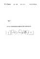
- FIG. 1is a schematic diagram of part of an optical communications system including a polarisation mode dispersion compensator
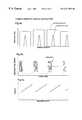
- FIG. 2is a schematic diagram showing in greater detail the polarisation mode dispersion compensator of FIG. 1 and including a differential delay system;
- FIG. 3is a schematic diagram showing a differential delay system for use in the compensator of FIG. 2 and comprising a differential delay element formed by a pair of chirped Bragg grating fibres;
- FIG. 3 ais a schematic graphical representation of grating pitch as a function of position for the differential delay element of FIG. 3;
- FIG. 4 ais a schematic graphical representation of the spectral profile of a grating fibre
- FIG. 4 bis a schematic graphical representation of the refractive index modulation of a fibre grating
- FIG. 4 cis a schematic graphical representation of differential delay as a function of wavelength in a chirped fibre grating
- FIG. 5 ais a schematic graphical representation of part of the spectral response of a sampled grating fibre
- FIG. 5 bis a schematic graphical representation of the refractive index profile of the sampled grating fibre of FIG. 5 a;
- FIG. 5 cis a schematic graphical representation of the delay characteristic as a function of wavelength for the sampled grating of FIGS. 5 a and 5 b;
- FIG. 6is a schematic representation of an alternative polarisation mode dispersion compensator using a single optical circulator
- FIG. 7is a schematic representation of a differential delay element with a single grating fibre
- FIG. 7 ais a schematic graphical representation of the variation of grating pitch with position for the element of FIG. 7;
- FIG. 8is a schematic representation of a differential delay element having an electro-mechanical transducer
- FIG. 9is a schematic representation of a further differential delay element having a thermal transducer
- FIG. 10is a schematic representation of a further differential delay element having fused fibres
- FIG. 10 ais a schematic graphical representation illustrating the variation of pitch with position for the fibre of FIG. 10;
- FIG. 11is a schematic representation of a further alternative differential delay element having a polarisation maintaining fibre
- FIG. 11 ais a schematic graphical representation of the grating pitch as a function of position for the separate modes conducted via the fibre of FIG. 11;
- FIG. 11 bis a schematic representation of the fibre of FIG. 11;
- FIG. 12is a schematic representation of an alternative embodiment of the polarization mode dispersion compensator of FIG. 1;
- FIG. 13shows a further alternative embodiment.
- an optical fibre 1provides a transmission path for propagation of an optical signal from a polarised light emitting transmitter 2 to a receiver 3 , this transmission path including an erbium doped optical fibre amplifier 4 and, adjacent the receiver 3 , a PMD (polarisation mode dispersion) compensator 5 .
- PMDpolarisation mode dispersion
- the optical fibre 1is a nominally circularly symmetric single mode fibre extending over a substantial distance, which in the present example is 100 km. Over a distance of this length the departures from perfect circular symmetry of that fibre, for example as a result of bending strain, are liable to be of a sufficient magnitude for the fibre to function as a concatenation of birefringent elements of random relative orientation. Moreover that orientation is liable to change with time.
- the transitis faster for one of the SOPs than for the other, and the difference in transit time is the polarisation mode dispersion of the concatenation.
- the launch SOPmaintained in the passage of the light through the concatenation, and the light emerges at the far end with an SOP that is in general different from that with which it was launched.
- the emergent SOP for one of the single transit time launch SOPsis orthogonal to the emergent SOP for the other single transit time launch SOP.
- the emergent lightis composed of two components (polarisation modes), generally of unequal amplitude, which have propagated through the concatenation with different transit times, respectively the previously mentioned fast and slow single transit times of the concatenation.
- the two single transit time launch SOPs for the concatenationare often referred to as the principle SOPs of the concatenation.
- the single transit time launch SOPsare, in general, different from the corresponding emergence SOPs, reference in this specification will be made to launch principal SOPs (LPSOPS) and to emergence principal SOPs (EPSOPs). From consideration of principles of reciprocity, it will be evident that the LPSOPs for one direction of propagation through the concatenation are the EPSOPs for the other, and vice versa.
- the input 6 of the PMD compensator 5is connected, within the compensator to a polarisation controller 7 operable to introduce a controlled amount of change of SOP from that received at input 6 so that delivered to a polarisation beam splitter 8 .
- the amount of change of SOP induced by polarisation controller 7is regulated by a control signal 9 from a controller 10 such that the polarisation controller maps the (time varying) EPSOPs of transmission path 1 substantially on to the principal SOPs of the polarisation beam splitter 8 so that the splitter operates to separate the polarisation modes emerging from the transmission path 1 , delivering from one output of the polarisation beam splitter 8 substantially exclusively the slow mode component 11 , and from the other output substantially exclusively the fast mode component 12 .
- Optical taps 13 and 14are arranged to sample the slow and fast mode components 11 and 12 respectively and detectors 15 and 16 provide conversion of optical tap signals to electrical inputs of a dispersion measurement signals to electrical inputs of a dispersion measurement circuit 17 .
- the optical signal conducted by the fibre 1consists of a series of optical pulses at 10 Gb/sec, the dispersion measurement circuit 17 being arranged to detect a dispersion interval t between the arrival of corresponding pulses in the slow and fast mode components 11 and 12 respectively.
- the term “dispersion”is used herein to mean “differential delay”.
- the measurement circuit 17outputs a signal 18 representative of the value of t to the controller 10 , thereby completing a control loop enabling the polarisation controller 7 to be regulated such that the value of signal 18 is a maximum.
- the slow and fast mode components 11 and 12are input to a differential delay system 19 which introduces unequal delays differing by an amount equal to the dispersion interval t and applied in an opposite sense so as to synchronise the data pulses in the respective components.
- Dispersion compensated outputs 20 and 21 from the differential delay system 19are combined in an optical recombiner 22 to form output optical signal 23 which is directed to the receiver 3 or may alternatively be routed via a further waveguide to a remote receiver or node of the communications system.
- the differential delay system 19is responsive to a control signal 24 from the controller 10 which is dependent upon the magnitude of the dispersion interval t and effects a continuously variable differential delay T.
- the differential delay system 19comprises first and second chirped Bragg grating fibres 25 and 26 which respectively constitute Bragg reflectors which introduce delays into the transmission of the slow and fast mode components 11 and 12 .
- the slow mode component 11is conducted by a waveguide 27 to a first optical circulator 28 which directs the incoming signal into a first end 29 of the first grating fibre 25 via a further waveguide 30 .
- the first chirped Bragg grating 25has a chirp characteristic A which is variable by means of a dimensional control element 32 , responsive to the control signal 24 to continuously vary the overall length of the fibre 25 and to correspondingly increase or decrease the grating pitch.
- the variation of grating pitch with lengthis illustrated graphically in FIG. 3A which illustrates for the purpose of the present example a linear chirp characteristic A of fibre 25 represented as a graph of grating pitch as a function of position along the length of the fibre.
- the dimensional control element 32by lengthening or shortening the fibre 25 , effects an increase or decrease in the grating pitch at each position along the length of the fibre.
- the reflection position 31is movable away from or towards the first end 29 of the fibre 25 respectively, thereby increasing or decreasing the delay time taken for the optical signal to travel between the first optical circulator 28 , the reflection position 31 and to return to the circulator 28 .
- a linear chirped characteristic B of the fibre 25illustrates the characteristic of the fibre in the absence of any perturbation being applied by the dimensional control elements 32 and therefore also corresponds to the characteristic of the second grating fibre 26 .
- the characteristic Ais elevated above characteristic B and therefore corresponds to an elongation of the fibre, the reflection position 31 of the first grating fibre corresponding to this elongation.
- the horizontal broken line Cindicates the grating pitch at which Bragg reflection occurs in the fibres 25 and 26 for light at wavelength ⁇ . From equation 1 it is apparent that any change in wavelength ⁇ will correspondingly result in a change in reflection position 31 , for example an increase in wavelength will move the reflection position further away from the first end 29 for a chirped grating in which the grating pitch increases with position relative to the first end.
- the slow mode component 11After being returned to the circulator 28 , the slow mode component 11 is routed by the circulator into a further waveguide conducting the dispersion compensated output 20 .
- the fast mode component 12is conducted by a waveguide 33 to a second optical circulator 34 which diverts the fast mode component via a further waveguide 35 to the first end 36 of the second grating fibre 26 .
- FIG. 3is only schematic and that the optical paths of waveguides 30 and 35 are intended to be identical.
- nis the refractive index of the fibre core and c is the speed of light.
- the first and second grating fibres 25 and 26 together with the dimensional control element 32 togethercomprise a differential delay element 38 suitable for compensating PMD.
- the delay element 38may however also have other uses in optical communication systems where a differential delay is required to be introduced between optical signals or components separated from a single optical signal.
- the length of the grating fibres 25 and 26is of the order of 1 cm and is suitable for correcting PMD occurring in a 10 Gb/sec data transmission with PMD having a maximum value of the order of 100 picosec. Approximately 1% strain is required to produce an extension of 100 microns providing the above delay. It is therefore apparent that such an arrangement has the advantage of being compact and requiring minimal physical movement to achieve the required range of delay. The delay is continuously variable and achievable with a rapid response time.
- the optical signalwill in practice have a finite bandwidth which must be taken into consideration when selecting the chirp characteristics of the grating fibres 25 and 26 .
- the reflection characteristics of the grating fibrehave a finite bandwidth as illustrated in FIG. 4 a which schematically shows a spectral profile of the reflection properties of a grating fibre with a linear chirp characteristic and for which the refractive index modulation defining the grating is uniform along the lengths of the grating as shown in FIG. 4 b .
- the delay introduced by the grating fibreis linearly dependent on wavelengths within the pass band of the grating fibre as shown in FIG. 4 c . The effect of this wavelength dependence may be utilised to provide compensation for chromatic dispersion in the optical signal.
- the amount of chromatic dispersionincreases with the amount of chirp present in the grating fibre, i.e. with the gradient of the chirp characteristic, so that in general a degree of chromatic dispersion compensation may be selected by design choice of the magnitude and sign of the gradient of chirp characteristic of the fibre.
- each of the signal componentsis preferable for each of the signal components to be subject to substantially the same value of differential delay T.
- Thismay be accomplished by modulating the envelope of the refractive index modulation in the fibre grating as illustrated in FIG. 5 b which illustrates the refractive index n as a function of distance along the grating fibre.
- the modulation of FIG. 5 bconsists of periods of sinusoidal modulation of fixed level envelope separated by intervals of zero modulation in a periodic manner.
- Such fibre gratingsare referred to as sampled gratings, or alternatively long period superstructure Bragg gratings, as described for example in Electronics Letters, Sept. 15, 1994, Vol. 30, No. 19 B. J. Eggleton et al, “Long Period Super Structure Bragg Gratings in Optical Fibres”.
- sampled gratingshave a frequency response characterised by a series of periodically spaced pass bands as illustrating schematically in FIG. 5a which, by appropriate modulation of the refractive index envelope in FIG. 5 b are selected to coincide substantially with the wavelengths of the multiplexed components of the optical signal.
- each pass bandhas substantially the same delay characteristic as a function of wavelength when reflected by Bragg reflection in fibres 25 and 26 described above.
- FIG. 6illustrates a PMD compensator using a single optical circulator 42 .
- the PMD compensator 40 of FIG. 6is connected to an optical communications system in the same manner as PMD compensator 5 in FIG. 1 and receives an input 6 , an output optical signal 23 subsequently being transmitted to a receiver 3 after compensation for PMD.
- the PMD compensator 40has a single optical circulator 42 which is a polarisation insensitive circulator which directs optical signals from the input 6 into a waveguide 41 which directs in turn the signal into a principal state separator 39 , corresponding to the separator 39 of FIG. 2 .
- Slow and fast mode components 11 and 12are output from the principal state separator 39 to a differential delay element 38 which may correspond to the element 38 shown in FIG. 3 or may comprise an alternative element described hereafter.
- An advantage of the arrangement of FIG. 6is that only a single circulator 42 is required and the provision of a separate optical recombiner 22 of FIG. 2 is no longer required since optical recombination is effected by means of the polarisation beam splitter 8 , acting as a Y coupler for the returning components 11 and 12 .
- the embodiment of FIG. 6may be configured to provide compensation in the case of single wavelength optical signals as discussed above with reference to FIG. 4 or wavelength division multiplexed signals as referred to above with reference to FIG. 5 .
- the differential delay element 45 of FIG. 7comprises a single chirped Bragg grating fibre 25 with a dimensional control element 32 regulated by a control signal 24 in the manner described above with reference to FIG. 3.
- a slow mode component 11is input to the grating fibre 25 and is subject to Bragg reflection with a variable delay dependent upon the value of signal 24 .
- a fast mode component 12is input to a waveguide 46 terminated in a simple reflector represented schematically by mirror 47 .
- the waveguide 46thereby provides a constant delay and the grating fibre 25 provides a variable delay so that the difference in delay between modes 11 and 12 is variable.
- This arrangementis clearly simpler in construction than the arrangement of FIG. 3 and would be suitable in systems where chromatic dispersion compensation was not required.
- the delay element 38 of FIG. 3however would be preferable if a relatively large amount of chromatic dispersion compensation was required since equal amounts of chromatic dispersion compensation are available to both slow and fast mode components 11 and 12 .
- FIG. 8illustrates a first example in which the first grating fibre 25 is clamped at its first end 29 relative to a support 48 .
- the dimensional control element 32consists of an electrically powered actuator 49 operable to apply tension to the fibre 25 by displacement of a second end 50 of the fibre relative to the support 48 .
- FIG. 9illustrates an alternative dimensional control element 32 in which fibre 25 is maintained at a variably controllable temperature by means of a temperature control circuit 51 connected to a thermal actuator 52 .
- the thermal actuator 52may simply be a resistive coating applied to the fibre.
- a second grating fibre 26remains uninfluenced by the dimensional control element 32 , thereby providing the reference against which the variable delay induced in the first fibre 25 creates a differential delay.
- FIG. 10shows an alternative arrangement in which the first and second grating fibres 25 and 26 are fused together in side by side configuration so as to co-extend along a support 48 to which the resulting fused fibre assembly 53 is clamped at a first end 54 .
- a dimensional control element 32is arranged to apply a bending moment to the fused fibre assembly 53 relative to the support 48 to effect bending in a plane common to the respective axes of the fibres 25 and 26 .
- bending in the direction of arrow 55for example will result in longitudinal extension of the first fibre 25 and longitudinal compression of the second fibre 26 , thereby increasing the pitch of the grating in first fibre 25 and decreasing the pitch in fibre 26 at each position along the length of the respective fibres.
- curve Bis the chirp characteristic for the unstrained fibres 25 and 26 and curves A 1 and A 2 are the chirped characteristics when strained in direction 55 .
- the dimensional control element 32 in FIG. 10may be any suitable electrically operable actuator such as a solenoid or piezoelectric device controlled by the control signal 24 .
- a further alternative differential delay element 56will now be described with reference to FIG. 11 using corresponding references to those of previous figures where appropriate for corresponding elements.
- wave guides 57 and 58 conducting the slow and fast mode components 11 and 12are coupled by means of a coupler 59 into a single polarisation maintaining fibre 60 such that the slow and fast mode components 11 and 12 are separately and orthogonally propagated as illustrated schematically in FIG. 11 b .
- a dimensional control element 32is arranged to apply a bending moment in the same manner described above with reference to the fused fibre assembly 53 of FIG. 10 .
- FIG. 11 ashows graphically the effect on the respective characteristics caused by bending, movement of the respective characteristic curves being indicated by arrows.
- FIG. 12illustrates schematically an alternative polarization mode dispersion compensator 70 which may be used as compensator 5 in the system of FIG. 1 .
- the compensator 70will be described using corresponding reference numerals to preceding figures where appropriate for corresponding elements.
- the compensator 70differs from the compensator of FIG. 2 in that the dispersion measurement circuit 17 of FIG. 2 measuring the input to the differential delay system 19 is replaced by a measurement circuit 71 which measures the output of a receiver 72 whose optical input has been subjected to compensation by differential delay system 19 .
- the measurement circuit 71provides a feedback signal 73 to the controller 10 which controls both the polarisation controller 7 and the differential delay system 19 .
- the compensator 70 of FIG. 12has therefore essentially a feedback configuration whereas the compensator of FIG. 2 has essentially a feed forward configuration. It will be apparent that, when the output of the compensator of FIG. 2 is connected to a receiver, the arrangement of FIG. 2 requires two detection stages, i.e. detection in the receiver and detection by the detectors 15 and 16 . The arrangement of FIG. 12 however includes a single detection stage, i.e. detection in the receiver 72 .
- the PMD compensator 70 of FIG. 12has an input waveguide 6 connected to a polarization controller 7 operable to introduce a controlled amount of change of polarization state of the optical signal as received.
- the output of the polarization controlleris diverted by an optical circulator 74 into a polarization beam splitter and recombiner 8 connected to output waveguides 75 and 76 such that the optical signal is divided into a slow mode component output in waveguide 75 and a fast mode component output in waveguide 76 , these components having polarization states corresponding substantially to the instantaneous emergence principal polarization states.
- the componentsAfter applying a differential delay by operation of the differential system 19 under the control of controller 10 , the components are returned to the recombiner 8 and the recombined output returned to the circulator 74 .
- the returned compensated outputis directed to the receiver 72 by the circulator 74 where the compensated output optical signal is detected.
- the measurement circuit 71derives from the electronic output of the receiver 72 a measure of the amount of signal degradation associated with polarization mode dispersion and any one of a number of techniques may be used.
- the measurement circuit 71may comprise an eye monitor responsive to the electrical signal output of the receiver 72 to obtain a measure of signal eye opening. Since the signal eye closes in the presence of dispersion, the eye monitor output provides an appropriate feedback signal 73 for control, the term dispersion here being used in the sense of pulse spreading.
- FIG. 13shows a further alternative PMD compensator 80 in which reference numerals corresponding to those of preceding figures are used where appropriate for corresponding elements.
- a polarization mode dispersion monitor 81receives an optical tap signal 82 and measures the amount of polarization mode dispersion to obtain the required feedback signal 73 .
- the PMD monitormay be of any one of a number of types and may for example comprise a monitor as disclosed in co-pending application US08/795684 filed Feb. 5, 1997.
- the optical output following differential delay and recombinationmay be input to a receiver (not shown) or may alternatively form an output signal for onward transmission in the optical communication system of FIG. 1 .
- the compensator 80 of FIG. 13is therefore particularly suited to providing PMD compensation at a node of a network at which no receiver is located.
- any one of the differential delay elements of FIGS. 7, 8 , 9 , 10 and 11may be used in a PMD compensator such as described above with reference to FIG. 2, 6 , 12 or 13 , using either a sampled or non-sampled chirped Bragg grating fibre according to whether wavelength multiplexed division transmission is required.
- the chirped characteristicmay be selected to provide a controlled amount of chromatic dispersion compensation if required.
- each of the above differential delay elementsincludes reflection of the slow and fast mode components 11 and 12 by Bragg reflection in a correspondingly chirped grating, thereby providing an inherent insensitivity to any fluctuation in wavelength of the optical signal since both fast and slow mode components will be subject to equivalent changes in delay due to wavelength fluctuation.
- one of the componentsis reflected by a simple reflector so that the point of reflection in the Bragg grating fibre 25 is sensitive to changes in wavelength in accordance with equation 1 .
- the feedback signalmay conveniently be transmitted optically in the fibre 1 in a direction opposite to that of the optical signal transmission.
- the electromagnetic solenoid actuator 49 referred to abovemay alternatively be replaced by a piezoelectric actuator.
- the thermal actuator 52 referred to abovemay alternatively comprise Peltier heating/cooling elements arranged to raise or lower the temperature of the fibre in a controlled manner in response to the signal 24 .
- the formation of the Bragg gratingmay alternatively be effected in a waveguide other than an optical fibre.
- Non-linear chirp characteristicsmay alternatively be utilised.
- the embodiments described with reference to FIG. 3, 8 and 9may alternatively include an additional dimensional control element operable on the second chirped Bragg grating fibre, the control actuation being preferably in an opposite sense to control of the first fibre.
Landscapes
- Physics & Mathematics (AREA)
- Electromagnetism (AREA)
- Engineering & Computer Science (AREA)
- Computer Networks & Wireless Communication (AREA)
- Signal Processing (AREA)
- Optical Communication System (AREA)
Abstract
Description


Claims (51)
Priority Applications (1)
| Application Number | Priority Date | Filing Date | Title |
|---|---|---|---|
| US09/135,967US6271952B1 (en) | 1998-08-18 | 1998-08-18 | Polarization mode dispersion compensation |
Applications Claiming Priority (1)
| Application Number | Priority Date | Filing Date | Title |
|---|---|---|---|
| US09/135,967US6271952B1 (en) | 1998-08-18 | 1998-08-18 | Polarization mode dispersion compensation |
Publications (1)
| Publication Number | Publication Date |
|---|---|
| US6271952B1true US6271952B1 (en) | 2001-08-07 |
Family
ID=22470613
Family Applications (1)
| Application Number | Title | Priority Date | Filing Date |
|---|---|---|---|
| US09/135,967Expired - LifetimeUS6271952B1 (en) | 1998-08-18 | 1998-08-18 | Polarization mode dispersion compensation |
Country Status (1)
| Country | Link |
|---|---|
| US (1) | US6271952B1 (en) |
Cited By (223)
| Publication number | Priority date | Publication date | Assignee | Title |
|---|---|---|---|---|
| US20010008452A1 (en)* | 2000-01-19 | 2001-07-19 | Takashi Sugihara | Wavelength multiplexing optical transmission system |
| US20020012487A1 (en)* | 2000-07-31 | 2002-01-31 | Yafo Networks, Inc. | Polarization mode dispersion generator |
| US6362874B1 (en)* | 2000-03-08 | 2002-03-26 | Lucent Technologies Inc. | Polarization mode dispersion measurement using phase-sensitive sideband detection |
| US6396606B1 (en)* | 1998-12-24 | 2002-05-28 | Worldcom, Inc. | Method of avoiding excessive polarization mode dispersion in an optical communications link |
| US6404520B1 (en)* | 1998-12-21 | 2002-06-11 | Mci Worldcom, Inc. | Fault isolation of an optical link by correlating PMD events with other measurements |
| US6411746B1 (en) | 2000-01-18 | 2002-06-25 | Corning Incorporated | Thermally tunable optical devices |
| US20020080467A1 (en)* | 2000-12-07 | 2002-06-27 | Yafo Networks, Inc. | Methods and apparatus for frequency shifting polarization mode dispersion spectra |
| US6459826B1 (en)* | 2000-03-21 | 2002-10-01 | Lucent Technologies Inc. | Programmable optical switch apparatus |
| US20020181878A1 (en)* | 2001-05-31 | 2002-12-05 | Schneider Victor M. | Dynamic chromatic dispersion control using coupled optical waveguides |
| US20020181860A1 (en)* | 2001-05-31 | 2002-12-05 | Weller-Brophy Laura A. | Chromatic dispersion control method and apparatus |
| US6493116B1 (en)* | 1999-02-09 | 2002-12-10 | Mci Worldcom, Inc. | PMD characterization across multiple optical channels of an optical link |
| US20020191285A1 (en)* | 2001-03-15 | 2002-12-19 | Yafo Networks, Inc. | Methods and apparatus for generating polarization mode dispersion |
| US6515778B1 (en)* | 1999-07-22 | 2003-02-04 | Nortel Networks Limited | Polarization mode dispersion compensation |
| US20030026543A1 (en)* | 2001-08-06 | 2003-02-06 | Alcatel | Tunable wideband dispersion compensator |
| US20030026533A1 (en)* | 2001-08-03 | 2003-02-06 | Yochay Danziger | Configurable dispersion management device |
| US20030059195A1 (en)* | 2001-08-29 | 2003-03-27 | Brennan James F. | Optical devices using shaped optical fibers and methods for making optical devices with shaped optical fibers |
| GB2380342A (en)* | 2001-09-28 | 2003-04-02 | Fujitsu Network Comm Inc | A compensator for polarisation-mode dispersion (PMD) compensation |
| US20030081291A1 (en)* | 2001-10-26 | 2003-05-01 | Nishimura Ken A. | Equalization of optical signals |
| US20030081891A1 (en)* | 2001-10-25 | 2003-05-01 | Schneider Vitor M. | Chromatic dispersion control using index variation |
| US20030095311A1 (en)* | 2001-11-16 | 2003-05-22 | Tiangong Liu | Hyrbid-integrated high-speed OTDM module |
| US6574015B1 (en)* | 1998-05-19 | 2003-06-03 | Seagate Technology Llc | Optical depolarizer |
| US20030122063A1 (en)* | 2001-12-31 | 2003-07-03 | Levent Biyikli | Polarization transformer and polarization mode dispersion compensator |
| US6590684B1 (en)* | 1999-06-30 | 2003-07-08 | Marconi Communications Limited | Optical system |
| WO2003058856A1 (en)* | 2001-12-31 | 2003-07-17 | 3M Innovative Properties Company | System for polarization mode dispersion compensation |
| US20030152385A1 (en)* | 2001-12-10 | 2003-08-14 | Louay Eldada | Wavelength division multiplexing optical performance monitors |
| US20030152320A1 (en)* | 2001-12-31 | 2003-08-14 | Debaun Barbara A. | System for higher-order dispersion compensation |
| US20030152322A1 (en)* | 2001-12-31 | 2003-08-14 | Smith Terry L. | System for higher-order dispersion compensation including a delay line |
| US20030152321A1 (en)* | 2001-12-31 | 2003-08-14 | Koch Barry J. | Method for higher-order dispersion compensation |
| WO2003040777A3 (en)* | 2001-11-02 | 2003-08-14 | Worldcom Inc | Integrated adaptive chromatic dispersion/polarization mode dispersion compensation system |
| US6609841B1 (en)* | 1998-03-30 | 2003-08-26 | Seagate Technology Llc | Low noise optical storage system based on an optical polarimetric delay line |
| US20030165284A1 (en)* | 2002-02-19 | 2003-09-04 | Mitsubishi Denki Kabushiki Kaisha | PMD compensating apparatus for controlling polarization controller based on detection of magnitude of waveform distortion |
| US20030184735A1 (en)* | 2001-12-28 | 2003-10-02 | Klaus Kotten | System and method for measuring and compensating for the polarization mode dispersion of an optical signal |
| US6633704B2 (en) | 2001-04-30 | 2003-10-14 | Corning Incorporated | Chromatic dispersion compensator |
| WO2003058857A3 (en)* | 2001-12-31 | 2003-10-16 | 3M Innovative Properties Co | System for higher-order dispersion compensation including a delay line |
| WO2003058311A3 (en)* | 2001-12-31 | 2003-10-16 | 3M Innovative Properties Co | System for higher-order dispersion compensation |
| WO2003088530A1 (en)* | 2002-04-18 | 2003-10-23 | Ericsson Telecomunicações S.A. | Polarization mode dispersion compensator |
| US20030223689A1 (en)* | 2001-12-31 | 2003-12-04 | Koch Barry J. | System for higher-order dispersion compensation including phase modulation |
| US20030223056A1 (en)* | 2002-05-31 | 2003-12-04 | Xiaoli Fu | Optical circuits for tunable second order PMD compensation and tunable dispersion compensation |
| US6674972B1 (en)* | 1999-09-01 | 2004-01-06 | At&T Corp. | Methods and systems for polarization mode dispersion compensation |
| US6707957B1 (en)* | 2001-12-18 | 2004-03-16 | Nortel Networks Limited | Compensating for polarisation mode dispersion in optical transmission fibers |
| US6710904B1 (en)* | 1999-07-08 | 2004-03-23 | Alcatel | System for compensating polarization dispersion in an optical transmission system |
| WO2003058855A3 (en)* | 2001-12-31 | 2004-03-25 | 3M Innovative Properties Co | Method for polarization mode dispersion compensation |
| WO2003093885A3 (en)* | 2002-04-29 | 2004-04-15 | Du Pont | Effective refractive index chirped bragg gratings |
| US6724972B2 (en) | 2001-12-31 | 2004-04-20 | 3M Innovative Properties Company | Silicate waveguide compositions for extended L-band and S-band amplification |
| US20040091272A1 (en)* | 2001-12-23 | 2004-05-13 | Heliang Liu | On-line dispersion compensation device for a wavelength division optical transmission system |
| US20040101241A1 (en)* | 2002-11-22 | 2004-05-27 | Kohnke Glenn E. | Fiber grating/DC fiber hybrid dispersion compensation module |
| US20040109220A1 (en)* | 2002-12-10 | 2004-06-10 | Ki Ho Han | PMD compensator based on separation of principal state of poloarization control and differential group delay control, and method thereof |
| US6778782B1 (en)* | 2000-09-27 | 2004-08-17 | Nortel Networks Limited | Dispersion compensation |
| US6867918B2 (en) | 2000-12-07 | 2005-03-15 | Jay N. Damask | Methods and apparatus for generation and control of coherent polarization mode dispersion |
| US6882760B2 (en) | 2001-06-29 | 2005-04-19 | Mitsubishi Denki Kabushiki Kaisha | Polarization dispersion compensating apparatus |
| US20050158055A1 (en)* | 2003-01-10 | 2005-07-21 | Fujitsu Limited | Optical communication system and optical communication method having confidentiality |
| US6947633B2 (en) | 2002-10-28 | 2005-09-20 | Optovia Corporation | Dispersion compensation |
| WO2006046947A3 (en)* | 2004-10-24 | 2006-06-01 | Chiral Photonics Inc | Chiral in-fiber polarizer apparatus and method |
| US20060250682A1 (en)* | 2005-03-18 | 2006-11-09 | Fujitsu Limited | Reducing polarization dependence of a wavelength dispersion variation monitor |
| US20060268392A1 (en)* | 2002-11-08 | 2006-11-30 | Dario Setti | Optical communication line and system with reduced polarization mode dispersion |
| US7263250B1 (en)* | 2002-10-18 | 2007-08-28 | Finisar Corporation | Optical switch using polarization beam splitters |
| US20080114556A1 (en)* | 2006-11-13 | 2008-05-15 | Lucent Technologies Inc. | Optical pulse characterization using phase modulation |
| US20080181615A1 (en)* | 2007-01-26 | 2008-07-31 | Bti Photonic Systems Inc. | Method and system for dynamic dispersion compensation |
| US20090252497A1 (en)* | 2008-04-08 | 2009-10-08 | Tellabs Operations, Inc. | Method and apparatus for compensating for polarization mode dispersion (PMD) |
| US20090285585A1 (en)* | 2008-05-13 | 2009-11-19 | Tellabs Operations, Inc. | Method and apparatus for polarization stabilization in optical receivers with complex modulation formats |
| US9154966B2 (en) | 2013-11-06 | 2015-10-06 | At&T Intellectual Property I, Lp | Surface-wave communications and methods thereof |
| US9209902B2 (en) | 2013-12-10 | 2015-12-08 | At&T Intellectual Property I, L.P. | Quasi-optical coupler |
| US9312919B1 (en) | 2014-10-21 | 2016-04-12 | At&T Intellectual Property I, Lp | Transmission device with impairment compensation and methods for use therewith |
| US9461706B1 (en) | 2015-07-31 | 2016-10-04 | At&T Intellectual Property I, Lp | Method and apparatus for exchanging communication signals |
| US9490869B1 (en) | 2015-05-14 | 2016-11-08 | At&T Intellectual Property I, L.P. | Transmission medium having multiple cores and methods for use therewith |
| US9503189B2 (en) | 2014-10-10 | 2016-11-22 | At&T Intellectual Property I, L.P. | Method and apparatus for arranging communication sessions in a communication system |
| US9509415B1 (en) | 2015-06-25 | 2016-11-29 | At&T Intellectual Property I, L.P. | Methods and apparatus for inducing a fundamental wave mode on a transmission medium |
| US9520945B2 (en) | 2014-10-21 | 2016-12-13 | At&T Intellectual Property I, L.P. | Apparatus for providing communication services and methods thereof |
| US9525210B2 (en) | 2014-10-21 | 2016-12-20 | At&T Intellectual Property I, L.P. | Guided-wave transmission device with non-fundamental mode propagation and methods for use therewith |
| US9525524B2 (en) | 2013-05-31 | 2016-12-20 | At&T Intellectual Property I, L.P. | Remote distributed antenna system |
| US9531427B2 (en) | 2014-11-20 | 2016-12-27 | At&T Intellectual Property I, L.P. | Transmission device with mode division multiplexing and methods for use therewith |
| US9564947B2 (en) | 2014-10-21 | 2017-02-07 | At&T Intellectual Property I, L.P. | Guided-wave transmission device with diversity and methods for use therewith |
| US9577306B2 (en) | 2014-10-21 | 2017-02-21 | At&T Intellectual Property I, L.P. | Guided-wave transmission device and methods for use therewith |
| US9608692B2 (en) | 2015-06-11 | 2017-03-28 | At&T Intellectual Property I, L.P. | Repeater and methods for use therewith |
| US9608740B2 (en) | 2015-07-15 | 2017-03-28 | At&T Intellectual Property I, L.P. | Method and apparatus for launching a wave mode that mitigates interference |
| US9615269B2 (en) | 2014-10-02 | 2017-04-04 | At&T Intellectual Property I, L.P. | Method and apparatus that provides fault tolerance in a communication network |
| US9628854B2 (en) | 2014-09-29 | 2017-04-18 | At&T Intellectual Property I, L.P. | Method and apparatus for distributing content in a communication network |
| US9628116B2 (en) | 2015-07-14 | 2017-04-18 | At&T Intellectual Property I, L.P. | Apparatus and methods for transmitting wireless signals |
| US9640850B2 (en) | 2015-06-25 | 2017-05-02 | At&T Intellectual Property I, L.P. | Methods and apparatus for inducing a non-fundamental wave mode on a transmission medium |
| US9654173B2 (en) | 2014-11-20 | 2017-05-16 | At&T Intellectual Property I, L.P. | Apparatus for powering a communication device and methods thereof |
| US9653770B2 (en) | 2014-10-21 | 2017-05-16 | At&T Intellectual Property I, L.P. | Guided wave coupler, coupling module and methods for use therewith |
| US9667317B2 (en) | 2015-06-15 | 2017-05-30 | At&T Intellectual Property I, L.P. | Method and apparatus for providing security using network traffic adjustments |
| US9680670B2 (en) | 2014-11-20 | 2017-06-13 | At&T Intellectual Property I, L.P. | Transmission device with channel equalization and control and methods for use therewith |
| US9685992B2 (en) | 2014-10-03 | 2017-06-20 | At&T Intellectual Property I, L.P. | Circuit panel network and methods thereof |
| US9692101B2 (en) | 2014-08-26 | 2017-06-27 | At&T Intellectual Property I, L.P. | Guided wave couplers for coupling electromagnetic waves between a waveguide surface and a surface of a wire |
| US9699785B2 (en) | 2012-12-05 | 2017-07-04 | At&T Intellectual Property I, L.P. | Backhaul link for distributed antenna system |
| US9705571B2 (en) | 2015-09-16 | 2017-07-11 | At&T Intellectual Property I, L.P. | Method and apparatus for use with a radio distributed antenna system |
| US9705561B2 (en) | 2015-04-24 | 2017-07-11 | At&T Intellectual Property I, L.P. | Directional coupling device and methods for use therewith |
| US9722318B2 (en) | 2015-07-14 | 2017-08-01 | At&T Intellectual Property I, L.P. | Method and apparatus for coupling an antenna to a device |
| US9729197B2 (en) | 2015-10-01 | 2017-08-08 | At&T Intellectual Property I, L.P. | Method and apparatus for communicating network management traffic over a network |
| US9735833B2 (en) | 2015-07-31 | 2017-08-15 | At&T Intellectual Property I, L.P. | Method and apparatus for communications management in a neighborhood network |
| US9742462B2 (en) | 2014-12-04 | 2017-08-22 | At&T Intellectual Property I, L.P. | Transmission medium and communication interfaces and methods for use therewith |
| US9749013B2 (en) | 2015-03-17 | 2017-08-29 | At&T Intellectual Property I, L.P. | Method and apparatus for reducing attenuation of electromagnetic waves guided by a transmission medium |
| US9749053B2 (en) | 2015-07-23 | 2017-08-29 | At&T Intellectual Property I, L.P. | Node device, repeater and methods for use therewith |
| US9748626B2 (en) | 2015-05-14 | 2017-08-29 | At&T Intellectual Property I, L.P. | Plurality of cables having different cross-sectional shapes which are bundled together to form a transmission medium |
| US9755697B2 (en) | 2014-09-15 | 2017-09-05 | At&T Intellectual Property I, L.P. | Method and apparatus for sensing a condition in a transmission medium of electromagnetic waves |
| US9762289B2 (en) | 2014-10-14 | 2017-09-12 | At&T Intellectual Property I, L.P. | Method and apparatus for transmitting or receiving signals in a transportation system |
| US9769128B2 (en) | 2015-09-28 | 2017-09-19 | At&T Intellectual Property I, L.P. | Method and apparatus for encryption of communications over a network |
| US9769020B2 (en) | 2014-10-21 | 2017-09-19 | At&T Intellectual Property I, L.P. | Method and apparatus for responding to events affecting communications in a communication network |
| US9780834B2 (en) | 2014-10-21 | 2017-10-03 | At&T Intellectual Property I, L.P. | Method and apparatus for transmitting electromagnetic waves |
| US9793951B2 (en) | 2015-07-15 | 2017-10-17 | At&T Intellectual Property I, L.P. | Method and apparatus for launching a wave mode that mitigates interference |
| US9793955B2 (en) | 2015-04-24 | 2017-10-17 | At&T Intellectual Property I, Lp | Passive electrical coupling device and methods for use therewith |
| US9793954B2 (en) | 2015-04-28 | 2017-10-17 | At&T Intellectual Property I, L.P. | Magnetic coupling device and methods for use therewith |
| US9800327B2 (en) | 2014-11-20 | 2017-10-24 | At&T Intellectual Property I, L.P. | Apparatus for controlling operations of a communication device and methods thereof |
| US9820146B2 (en) | 2015-06-12 | 2017-11-14 | At&T Intellectual Property I, L.P. | Method and apparatus for authentication and identity management of communicating devices |
| US9838896B1 (en) | 2016-12-09 | 2017-12-05 | At&T Intellectual Property I, L.P. | Method and apparatus for assessing network coverage |
| US9836957B2 (en) | 2015-07-14 | 2017-12-05 | At&T Intellectual Property I, L.P. | Method and apparatus for communicating with premises equipment |
| US9847566B2 (en) | 2015-07-14 | 2017-12-19 | At&T Intellectual Property I, L.P. | Method and apparatus for adjusting a field of a signal to mitigate interference |
| US9847850B2 (en) | 2014-10-14 | 2017-12-19 | At&T Intellectual Property I, L.P. | Method and apparatus for adjusting a mode of communication in a communication network |
| US9853342B2 (en) | 2015-07-14 | 2017-12-26 | At&T Intellectual Property I, L.P. | Dielectric transmission medium connector and methods for use therewith |
| US9860075B1 (en) | 2016-08-26 | 2018-01-02 | At&T Intellectual Property I, L.P. | Method and communication node for broadband distribution |
| US9865911B2 (en) | 2015-06-25 | 2018-01-09 | At&T Intellectual Property I, L.P. | Waveguide system for slot radiating first electromagnetic waves that are combined into a non-fundamental wave mode second electromagnetic wave on a transmission medium |
| US9866309B2 (en) | 2015-06-03 | 2018-01-09 | At&T Intellectual Property I, Lp | Host node device and methods for use therewith |
| US9871283B2 (en) | 2015-07-23 | 2018-01-16 | At&T Intellectual Property I, Lp | Transmission medium having a dielectric core comprised of plural members connected by a ball and socket configuration |
| US9871282B2 (en) | 2015-05-14 | 2018-01-16 | At&T Intellectual Property I, L.P. | At least one transmission medium having a dielectric surface that is covered at least in part by a second dielectric |
| US9876570B2 (en) | 2015-02-20 | 2018-01-23 | At&T Intellectual Property I, Lp | Guided-wave transmission device with non-fundamental mode propagation and methods for use therewith |
| US9876264B2 (en) | 2015-10-02 | 2018-01-23 | At&T Intellectual Property I, Lp | Communication system, guided wave switch and methods for use therewith |
| US9876605B1 (en) | 2016-10-21 | 2018-01-23 | At&T Intellectual Property I, L.P. | Launcher and coupling system to support desired guided wave mode |
| US9882257B2 (en) | 2015-07-14 | 2018-01-30 | At&T Intellectual Property I, L.P. | Method and apparatus for launching a wave mode that mitigates interference |
| US9882277B2 (en) | 2015-10-02 | 2018-01-30 | At&T Intellectual Property I, Lp | Communication device and antenna assembly with actuated gimbal mount |
| US9893795B1 (en) | 2016-12-07 | 2018-02-13 | At&T Intellectual Property I, Lp | Method and repeater for broadband distribution |
| US9906269B2 (en) | 2014-09-17 | 2018-02-27 | At&T Intellectual Property I, L.P. | Monitoring and mitigating conditions in a communication network |
| US9904535B2 (en) | 2015-09-14 | 2018-02-27 | At&T Intellectual Property I, L.P. | Method and apparatus for distributing software |
| US9912419B1 (en) | 2016-08-24 | 2018-03-06 | At&T Intellectual Property I, L.P. | Method and apparatus for managing a fault in a distributed antenna system |
| US9913139B2 (en) | 2015-06-09 | 2018-03-06 | At&T Intellectual Property I, L.P. | Signal fingerprinting for authentication of communicating devices |
| US9912382B2 (en) | 2015-06-03 | 2018-03-06 | At&T Intellectual Property I, Lp | Network termination and methods for use therewith |
| US9911020B1 (en) | 2016-12-08 | 2018-03-06 | At&T Intellectual Property I, L.P. | Method and apparatus for tracking via a radio frequency identification device |
| US9912027B2 (en) | 2015-07-23 | 2018-03-06 | At&T Intellectual Property I, L.P. | Method and apparatus for exchanging communication signals |
| US9917341B2 (en) | 2015-05-27 | 2018-03-13 | At&T Intellectual Property I, L.P. | Apparatus and method for launching electromagnetic waves and for modifying radial dimensions of the propagating electromagnetic waves |
| US9927517B1 (en) | 2016-12-06 | 2018-03-27 | At&T Intellectual Property I, L.P. | Apparatus and methods for sensing rainfall |
| US9948354B2 (en) | 2015-04-28 | 2018-04-17 | At&T Intellectual Property I, L.P. | Magnetic coupling device with reflective plate and methods for use therewith |
| US9948333B2 (en) | 2015-07-23 | 2018-04-17 | At&T Intellectual Property I, L.P. | Method and apparatus for wireless communications to mitigate interference |
| US9954287B2 (en) | 2014-11-20 | 2018-04-24 | At&T Intellectual Property I, L.P. | Apparatus for converting wireless signals and electromagnetic waves and methods thereof |
| US9967173B2 (en) | 2015-07-31 | 2018-05-08 | At&T Intellectual Property I, L.P. | Method and apparatus for authentication and identity management of communicating devices |
| US9973940B1 (en) | 2017-02-27 | 2018-05-15 | At&T Intellectual Property I, L.P. | Apparatus and methods for dynamic impedance matching of a guided wave launcher |
| US9991580B2 (en) | 2016-10-21 | 2018-06-05 | At&T Intellectual Property I, L.P. | Launcher and coupling system for guided wave mode cancellation |
| US9999038B2 (en) | 2013-05-31 | 2018-06-12 | At&T Intellectual Property I, L.P. | Remote distributed antenna system |
| US9998870B1 (en) | 2016-12-08 | 2018-06-12 | At&T Intellectual Property I, L.P. | Method and apparatus for proximity sensing |
| US9997819B2 (en) | 2015-06-09 | 2018-06-12 | At&T Intellectual Property I, L.P. | Transmission medium and method for facilitating propagation of electromagnetic waves via a core |
| US10009901B2 (en) | 2015-09-16 | 2018-06-26 | At&T Intellectual Property I, L.P. | Method, apparatus, and computer-readable storage medium for managing utilization of wireless resources between base stations |
| US10009065B2 (en) | 2012-12-05 | 2018-06-26 | At&T Intellectual Property I, L.P. | Backhaul link for distributed antenna system |
| US10009067B2 (en) | 2014-12-04 | 2018-06-26 | At&T Intellectual Property I, L.P. | Method and apparatus for configuring a communication interface |
| US10009063B2 (en) | 2015-09-16 | 2018-06-26 | At&T Intellectual Property I, L.P. | Method and apparatus for use with a radio distributed antenna system having an out-of-band reference signal |
| US10020844B2 (en) | 2016-12-06 | 2018-07-10 | T&T Intellectual Property I, L.P. | Method and apparatus for broadcast communication via guided waves |
| US10020587B2 (en) | 2015-07-31 | 2018-07-10 | At&T Intellectual Property I, L.P. | Radial antenna and methods for use therewith |
| US10027397B2 (en) | 2016-12-07 | 2018-07-17 | At&T Intellectual Property I, L.P. | Distributed antenna system and methods for use therewith |
| US10033107B2 (en) | 2015-07-14 | 2018-07-24 | At&T Intellectual Property I, L.P. | Method and apparatus for coupling an antenna to a device |
| US10033108B2 (en) | 2015-07-14 | 2018-07-24 | At&T Intellectual Property I, L.P. | Apparatus and methods for generating an electromagnetic wave having a wave mode that mitigates interference |
| US10044409B2 (en) | 2015-07-14 | 2018-08-07 | At&T Intellectual Property I, L.P. | Transmission medium and methods for use therewith |
| US10051629B2 (en) | 2015-09-16 | 2018-08-14 | At&T Intellectual Property I, L.P. | Method and apparatus for use with a radio distributed antenna system having an in-band reference signal |
| US10051483B2 (en) | 2015-10-16 | 2018-08-14 | At&T Intellectual Property I, L.P. | Method and apparatus for directing wireless signals |
| US10069535B2 (en) | 2016-12-08 | 2018-09-04 | At&T Intellectual Property I, L.P. | Apparatus and methods for launching electromagnetic waves having a certain electric field structure |
| US10074890B2 (en) | 2015-10-02 | 2018-09-11 | At&T Intellectual Property I, L.P. | Communication device and antenna with integrated light assembly |
| US10079661B2 (en) | 2015-09-16 | 2018-09-18 | At&T Intellectual Property I, L.P. | Method and apparatus for use with a radio distributed antenna system having a clock reference |
| US10090594B2 (en) | 2016-11-23 | 2018-10-02 | At&T Intellectual Property I, L.P. | Antenna system having structural configurations for assembly |
| US10090606B2 (en) | 2015-07-15 | 2018-10-02 | At&T Intellectual Property I, L.P. | Antenna system with dielectric array and methods for use therewith |
| US10103801B2 (en) | 2015-06-03 | 2018-10-16 | At&T Intellectual Property I, L.P. | Host node device and methods for use therewith |
| US10103422B2 (en) | 2016-12-08 | 2018-10-16 | At&T Intellectual Property I, L.P. | Method and apparatus for mounting network devices |
| US10135146B2 (en) | 2016-10-18 | 2018-11-20 | At&T Intellectual Property I, L.P. | Apparatus and methods for launching guided waves via circuits |
| US10135147B2 (en) | 2016-10-18 | 2018-11-20 | At&T Intellectual Property I, L.P. | Apparatus and methods for launching guided waves via an antenna |
| US10136434B2 (en) | 2015-09-16 | 2018-11-20 | At&T Intellectual Property I, L.P. | Method and apparatus for use with a radio distributed antenna system having an ultra-wideband control channel |
| US10135145B2 (en) | 2016-12-06 | 2018-11-20 | At&T Intellectual Property I, L.P. | Apparatus and methods for generating an electromagnetic wave along a transmission medium |
| US10139820B2 (en) | 2016-12-07 | 2018-11-27 | At&T Intellectual Property I, L.P. | Method and apparatus for deploying equipment of a communication system |
| US10142086B2 (en) | 2015-06-11 | 2018-11-27 | At&T Intellectual Property I, L.P. | Repeater and methods for use therewith |
| US10148016B2 (en) | 2015-07-14 | 2018-12-04 | At&T Intellectual Property I, L.P. | Apparatus and methods for communicating utilizing an antenna array |
| US10144036B2 (en) | 2015-01-30 | 2018-12-04 | At&T Intellectual Property I, L.P. | Method and apparatus for mitigating interference affecting a propagation of electromagnetic waves guided by a transmission medium |
| US10154493B2 (en) | 2015-06-03 | 2018-12-11 | At&T Intellectual Property I, L.P. | Network termination and methods for use therewith |
| US10168695B2 (en) | 2016-12-07 | 2019-01-01 | At&T Intellectual Property I, L.P. | Method and apparatus for controlling an unmanned aircraft |
| US10170840B2 (en) | 2015-07-14 | 2019-01-01 | At&T Intellectual Property I, L.P. | Apparatus and methods for sending or receiving electromagnetic signals |
| US10178445B2 (en) | 2016-11-23 | 2019-01-08 | At&T Intellectual Property I, L.P. | Methods, devices, and systems for load balancing between a plurality of waveguides |
| US10205655B2 (en) | 2015-07-14 | 2019-02-12 | At&T Intellectual Property I, L.P. | Apparatus and methods for communicating utilizing an antenna array and multiple communication paths |
| US10224634B2 (en) | 2016-11-03 | 2019-03-05 | At&T Intellectual Property I, L.P. | Methods and apparatus for adjusting an operational characteristic of an antenna |
| US10225025B2 (en) | 2016-11-03 | 2019-03-05 | At&T Intellectual Property I, L.P. | Method and apparatus for detecting a fault in a communication system |
| US10243270B2 (en) | 2016-12-07 | 2019-03-26 | At&T Intellectual Property I, L.P. | Beam adaptive multi-feed dielectric antenna system and methods for use therewith |
| US10243784B2 (en) | 2014-11-20 | 2019-03-26 | At&T Intellectual Property I, L.P. | System for generating topology information and methods thereof |
| US10264586B2 (en) | 2016-12-09 | 2019-04-16 | At&T Mobility Ii Llc | Cloud-based packet controller and methods for use therewith |
| US10291334B2 (en) | 2016-11-03 | 2019-05-14 | At&T Intellectual Property I, L.P. | System for detecting a fault in a communication system |
| US10291311B2 (en) | 2016-09-09 | 2019-05-14 | At&T Intellectual Property I, L.P. | Method and apparatus for mitigating a fault in a distributed antenna system |
| US10298293B2 (en) | 2017-03-13 | 2019-05-21 | At&T Intellectual Property I, L.P. | Apparatus of communication utilizing wireless network devices |
| US10305190B2 (en) | 2016-12-01 | 2019-05-28 | At&T Intellectual Property I, L.P. | Reflecting dielectric antenna system and methods for use therewith |
| US10312567B2 (en) | 2016-10-26 | 2019-06-04 | At&T Intellectual Property I, L.P. | Launcher with planar strip antenna and methods for use therewith |
| US10320586B2 (en) | 2015-07-14 | 2019-06-11 | At&T Intellectual Property I, L.P. | Apparatus and methods for generating non-interfering electromagnetic waves on an insulated transmission medium |
| US10326689B2 (en) | 2016-12-08 | 2019-06-18 | At&T Intellectual Property I, L.P. | Method and system for providing alternative communication paths |
| US10326494B2 (en) | 2016-12-06 | 2019-06-18 | At&T Intellectual Property I, L.P. | Apparatus for measurement de-embedding and methods for use therewith |
| US10340983B2 (en) | 2016-12-09 | 2019-07-02 | At&T Intellectual Property I, L.P. | Method and apparatus for surveying remote sites via guided wave communications |
| US10340603B2 (en) | 2016-11-23 | 2019-07-02 | At&T Intellectual Property I, L.P. | Antenna system having shielded structural configurations for assembly |
| US10341142B2 (en) | 2015-07-14 | 2019-07-02 | At&T Intellectual Property I, L.P. | Apparatus and methods for generating non-interfering electromagnetic waves on an uninsulated conductor |
| US10340601B2 (en) | 2016-11-23 | 2019-07-02 | At&T Intellectual Property I, L.P. | Multi-antenna system and methods for use therewith |
| US10340600B2 (en) | 2016-10-18 | 2019-07-02 | At&T Intellectual Property I, L.P. | Apparatus and methods for launching guided waves via plural waveguide systems |
| US10340573B2 (en) | 2016-10-26 | 2019-07-02 | At&T Intellectual Property I, L.P. | Launcher with cylindrical coupling device and methods for use therewith |
| US10348391B2 (en) | 2015-06-03 | 2019-07-09 | At&T Intellectual Property I, L.P. | Client node device with frequency conversion and methods for use therewith |
| US10355367B2 (en) | 2015-10-16 | 2019-07-16 | At&T Intellectual Property I, L.P. | Antenna structure for exchanging wireless signals |
| US10361489B2 (en) | 2016-12-01 | 2019-07-23 | At&T Intellectual Property I, L.P. | Dielectric dish antenna system and methods for use therewith |
| US10359749B2 (en) | 2016-12-07 | 2019-07-23 | At&T Intellectual Property I, L.P. | Method and apparatus for utilities management via guided wave communication |
| US10374316B2 (en) | 2016-10-21 | 2019-08-06 | At&T Intellectual Property I, L.P. | System and dielectric antenna with non-uniform dielectric |
| US10382976B2 (en) | 2016-12-06 | 2019-08-13 | At&T Intellectual Property I, L.P. | Method and apparatus for managing wireless communications based on communication paths and network device positions |
| US10389037B2 (en) | 2016-12-08 | 2019-08-20 | At&T Intellectual Property I, L.P. | Apparatus and methods for selecting sections of an antenna array and use therewith |
| US10389029B2 (en) | 2016-12-07 | 2019-08-20 | At&T Intellectual Property I, L.P. | Multi-feed dielectric antenna system with core selection and methods for use therewith |
| US10396887B2 (en) | 2015-06-03 | 2019-08-27 | At&T Intellectual Property I, L.P. | Client node device and methods for use therewith |
| US10411356B2 (en) | 2016-12-08 | 2019-09-10 | At&T Intellectual Property I, L.P. | Apparatus and methods for selectively targeting communication devices with an antenna array |
| US10439675B2 (en) | 2016-12-06 | 2019-10-08 | At&T Intellectual Property I, L.P. | Method and apparatus for repeating guided wave communication signals |
| US10446936B2 (en) | 2016-12-07 | 2019-10-15 | At&T Intellectual Property I, L.P. | Multi-feed dielectric antenna system and methods for use therewith |
| US10498044B2 (en) | 2016-11-03 | 2019-12-03 | At&T Intellectual Property I, L.P. | Apparatus for configuring a surface of an antenna |
| US10530505B2 (en) | 2016-12-08 | 2020-01-07 | At&T Intellectual Property I, L.P. | Apparatus and methods for launching electromagnetic waves along a transmission medium |
| US10535928B2 (en) | 2016-11-23 | 2020-01-14 | At&T Intellectual Property I, L.P. | Antenna system and methods for use therewith |
| US10547348B2 (en) | 2016-12-07 | 2020-01-28 | At&T Intellectual Property I, L.P. | Method and apparatus for switching transmission mediums in a communication system |
| US10601494B2 (en) | 2016-12-08 | 2020-03-24 | At&T Intellectual Property I, L.P. | Dual-band communication device and method for use therewith |
| US10637149B2 (en) | 2016-12-06 | 2020-04-28 | At&T Intellectual Property I, L.P. | Injection molded dielectric antenna and methods for use therewith |
| US10650940B2 (en) | 2015-05-15 | 2020-05-12 | At&T Intellectual Property I, L.P. | Transmission medium having a conductive material and methods for use therewith |
| US10665942B2 (en) | 2015-10-16 | 2020-05-26 | At&T Intellectual Property I, L.P. | Method and apparatus for adjusting wireless communications |
| EP3508896A4 (en)* | 2016-08-30 | 2020-06-03 | Fujikura Ltd. | Chirped fiber grating element and fiber laser |
| US10679767B2 (en) | 2015-05-15 | 2020-06-09 | At&T Intellectual Property I, L.P. | Transmission medium having a conductive material and methods for use therewith |
| US10694379B2 (en) | 2016-12-06 | 2020-06-23 | At&T Intellectual Property I, L.P. | Waveguide system with device-based authentication and methods for use therewith |
| US10727599B2 (en) | 2016-12-06 | 2020-07-28 | At&T Intellectual Property I, L.P. | Launcher with slot antenna and methods for use therewith |
| US10755542B2 (en) | 2016-12-06 | 2020-08-25 | At&T Intellectual Property I, L.P. | Method and apparatus for surveillance via guided wave communication |
| CN111638575A (en)* | 2020-07-03 | 2020-09-08 | 中国电子科技集团公司第三十八研究所 | Light time delay array chip based on chirp Bragg grating |
| US10777873B2 (en) | 2016-12-08 | 2020-09-15 | At&T Intellectual Property I, L.P. | Method and apparatus for mounting network devices |
| US10784670B2 (en) | 2015-07-23 | 2020-09-22 | At&T Intellectual Property I, L.P. | Antenna support for aligning an antenna |
| US10811767B2 (en) | 2016-10-21 | 2020-10-20 | At&T Intellectual Property I, L.P. | System and dielectric antenna with convex dielectric radome |
| US10819035B2 (en) | 2016-12-06 | 2020-10-27 | At&T Intellectual Property I, L.P. | Launcher with helical antenna and methods for use therewith |
| US10916969B2 (en) | 2016-12-08 | 2021-02-09 | At&T Intellectual Property I, L.P. | Method and apparatus for providing power using an inductive coupling |
| US10938108B2 (en) | 2016-12-08 | 2021-03-02 | At&T Intellectual Property I, L.P. | Frequency selective multi-feed dielectric antenna system and methods for use therewith |
| US11032819B2 (en) | 2016-09-15 | 2021-06-08 | At&T Intellectual Property I, L.P. | Method and apparatus for use with a radio distributed antenna system having a control channel reference signal |
Citations (2)
| Publication number | Priority date | Publication date | Assignee | Title |
|---|---|---|---|---|
| US5715265A (en)* | 1995-09-26 | 1998-02-03 | Northern Telecom Limited | Dispersion compensation |
| US5822100A (en)* | 1996-06-26 | 1998-10-13 | Mci Communications Corporation | Method and system for equalizing PMD using incremental delay switching |
- 1998
- 1998-08-18USUS09/135,967patent/US6271952B1/ennot_activeExpired - Lifetime
Patent Citations (2)
| Publication number | Priority date | Publication date | Assignee | Title |
|---|---|---|---|---|
| US5715265A (en)* | 1995-09-26 | 1998-02-03 | Northern Telecom Limited | Dispersion compensation |
| US5822100A (en)* | 1996-06-26 | 1998-10-13 | Mci Communications Corporation | Method and system for equalizing PMD using incremental delay switching |
Non-Patent Citations (2)
| Title |
|---|
| Takahashi, J., et al., "Automatic Compensation Technique for Timewise Fluctuating Polarisation Mode Disperson in in-line Amplifier Systems," Electronics Letters, Feb. 17th, 1994, vol. 30, No. 4, pp. 348-349. |
| Yoshimura, et al., "Polarization Mode Disperson Equalization," Fifth Optoelectronics Conference (Dec. 1994) Technical Digest, Jul. 1994, Makuhari Messe, pp. 258-259. |
Cited By (326)
| Publication number | Priority date | Publication date | Assignee | Title |
|---|---|---|---|---|
| US6609841B1 (en)* | 1998-03-30 | 2003-08-26 | Seagate Technology Llc | Low noise optical storage system based on an optical polarimetric delay line |
| US6574015B1 (en)* | 1998-05-19 | 2003-06-03 | Seagate Technology Llc | Optical depolarizer |
| US6570682B2 (en)* | 1998-12-21 | 2003-05-27 | Worldcom, Inc. | Fault isolation of an optical link by correlating PMD events with other measurements |
| US6404520B1 (en)* | 1998-12-21 | 2002-06-11 | Mci Worldcom, Inc. | Fault isolation of an optical link by correlating PMD events with other measurements |
| US6396606B1 (en)* | 1998-12-24 | 2002-05-28 | Worldcom, Inc. | Method of avoiding excessive polarization mode dispersion in an optical communications link |
| US6681081B2 (en) | 1998-12-24 | 2004-01-20 | Worldcom, Inc. | Method of avoiding excessive polarization mode dispersion in an optical communications link |
| US6493116B1 (en)* | 1999-02-09 | 2002-12-10 | Mci Worldcom, Inc. | PMD characterization across multiple optical channels of an optical link |
| US6704510B2 (en) | 1999-02-09 | 2004-03-09 | Worldcom, Inc. | PMD characterization across multiple optical channels of an optical link |
| US6590684B1 (en)* | 1999-06-30 | 2003-07-08 | Marconi Communications Limited | Optical system |
| US6710904B1 (en)* | 1999-07-08 | 2004-03-23 | Alcatel | System for compensating polarization dispersion in an optical transmission system |
| US6515778B1 (en)* | 1999-07-22 | 2003-02-04 | Nortel Networks Limited | Polarization mode dispersion compensation |
| US6674972B1 (en)* | 1999-09-01 | 2004-01-06 | At&T Corp. | Methods and systems for polarization mode dispersion compensation |
| US6411746B1 (en) | 2000-01-18 | 2002-06-25 | Corning Incorporated | Thermally tunable optical devices |
| US20010008452A1 (en)* | 2000-01-19 | 2001-07-19 | Takashi Sugihara | Wavelength multiplexing optical transmission system |
| US6362874B1 (en)* | 2000-03-08 | 2002-03-26 | Lucent Technologies Inc. | Polarization mode dispersion measurement using phase-sensitive sideband detection |
| US6459826B1 (en)* | 2000-03-21 | 2002-10-01 | Lucent Technologies Inc. | Programmable optical switch apparatus |
| US20020012487A1 (en)* | 2000-07-31 | 2002-01-31 | Yafo Networks, Inc. | Polarization mode dispersion generator |
| US6778782B1 (en)* | 2000-09-27 | 2004-08-17 | Nortel Networks Limited | Dispersion compensation |
| US6867918B2 (en) | 2000-12-07 | 2005-03-15 | Jay N. Damask | Methods and apparatus for generation and control of coherent polarization mode dispersion |
| US6891674B2 (en) | 2000-12-07 | 2005-05-10 | Yafo Networks, Inc. | Methods and apparatus for frequency shifting polarization mode dispersion spectra |
| US20020080467A1 (en)* | 2000-12-07 | 2002-06-27 | Yafo Networks, Inc. | Methods and apparatus for frequency shifting polarization mode dispersion spectra |
| US20020191285A1 (en)* | 2001-03-15 | 2002-12-19 | Yafo Networks, Inc. | Methods and apparatus for generating polarization mode dispersion |
| US6847484B2 (en) | 2001-03-15 | 2005-01-25 | Jay N. Damask | Methods and apparatus for generating polarization mode dispersion |
| US6633704B2 (en) | 2001-04-30 | 2003-10-14 | Corning Incorporated | Chromatic dispersion compensator |
| US20020181878A1 (en)* | 2001-05-31 | 2002-12-05 | Schneider Victor M. | Dynamic chromatic dispersion control using coupled optical waveguides |
| US20020181860A1 (en)* | 2001-05-31 | 2002-12-05 | Weller-Brophy Laura A. | Chromatic dispersion control method and apparatus |
| US6882760B2 (en) | 2001-06-29 | 2005-04-19 | Mitsubishi Denki Kabushiki Kaisha | Polarization dispersion compensating apparatus |
| US20030026533A1 (en)* | 2001-08-03 | 2003-02-06 | Yochay Danziger | Configurable dispersion management device |
| US20030026543A1 (en)* | 2001-08-06 | 2003-02-06 | Alcatel | Tunable wideband dispersion compensator |
| US20030059195A1 (en)* | 2001-08-29 | 2003-03-27 | Brennan James F. | Optical devices using shaped optical fibers and methods for making optical devices with shaped optical fibers |
| WO2003021317A3 (en)* | 2001-08-29 | 2003-10-16 | 3M Innovative Properties Co | Optical devices using shaped optical fibers and methods for making optical devices with shaped optical fibers |
| US7218800B2 (en) | 2001-09-28 | 2007-05-15 | Fujitsu Limited | Compensator for polarization-mode dispersion compensation |
| GB2380342A (en)* | 2001-09-28 | 2003-04-02 | Fujitsu Network Comm Inc | A compensator for polarisation-mode dispersion (PMD) compensation |
| GB2380342B (en)* | 2001-09-28 | 2005-08-10 | Fujitsu Network Comm Inc | A compensator for polarisation-mode dispersion compensation |
| WO2003030410A3 (en)* | 2001-09-28 | 2003-10-16 | Fujitsu Ltd | Compensator for polarisation-mode dispersion compensation |
| EP1786122A3 (en)* | 2001-09-28 | 2007-07-04 | Fujitsu Limited | A compensator for polarization-mode dispersion compensation |
| US20050002594A1 (en)* | 2001-09-28 | 2005-01-06 | Parker Michael C. | Compensator for polarisation-mode dispersion compensation |
| US20030081891A1 (en)* | 2001-10-25 | 2003-05-01 | Schneider Vitor M. | Chromatic dispersion control using index variation |
| US20030081291A1 (en)* | 2001-10-26 | 2003-05-01 | Nishimura Ken A. | Equalization of optical signals |
| US7272324B2 (en)* | 2001-10-26 | 2007-09-18 | Avago Technologies Fiber Ip (Singapore) Pte. Ltd. | Equalization of optical signals |
| US6889011B1 (en) | 2001-11-02 | 2005-05-03 | Mci, Inc. | Integrated adaptive chromatic dispersion/polarization mode dispersion compensation system |
| WO2003040777A3 (en)* | 2001-11-02 | 2003-08-14 | Worldcom Inc | Integrated adaptive chromatic dispersion/polarization mode dispersion compensation system |
| US20030095311A1 (en)* | 2001-11-16 | 2003-05-22 | Tiangong Liu | Hyrbid-integrated high-speed OTDM module |
| US7127174B2 (en)* | 2001-11-16 | 2006-10-24 | Oplink Communications, Inc. | Hybrid-integrated high-speed OTDM module |
| US7167647B2 (en)* | 2001-12-10 | 2007-01-23 | E. I. Du Pont De Nemours And Company | Wavelength division multiplexing optical performance monitors |
| US20030152385A1 (en)* | 2001-12-10 | 2003-08-14 | Louay Eldada | Wavelength division multiplexing optical performance monitors |
| US6707957B1 (en)* | 2001-12-18 | 2004-03-16 | Nortel Networks Limited | Compensating for polarisation mode dispersion in optical transmission fibers |
| US7221872B2 (en)* | 2001-12-23 | 2007-05-22 | Huawei Technologies Co., Ltd. | On-line dispersion compensation device for a wavelength division optical transmission system |
| US20040091272A1 (en)* | 2001-12-23 | 2004-05-13 | Heliang Liu | On-line dispersion compensation device for a wavelength division optical transmission system |
| DE10164497B4 (en)* | 2001-12-28 | 2005-03-10 | Siemens Ag | Arrangement and method for measuring and compensating the polarization mode dispersion of an optical signal |
| EP1324517A3 (en)* | 2001-12-28 | 2006-04-12 | Siemens Aktiengesellschaft | Arrangement and Method for measuring and compensating the Polarisation Mode Dispersion of optical signals |
| US6972835B2 (en)* | 2001-12-28 | 2005-12-06 | Siemens Aktiengesellschaft | System and method for measuring and compensating for the polarization mode dispersion of an optical signal |
| US20030184735A1 (en)* | 2001-12-28 | 2003-10-02 | Klaus Kotten | System and method for measuring and compensating for the polarization mode dispersion of an optical signal |
| US20030152320A1 (en)* | 2001-12-31 | 2003-08-14 | Debaun Barbara A. | System for higher-order dispersion compensation |
| CN1316769C (en)* | 2001-12-31 | 2007-05-16 | 3M创新有限公司 | System for polarization mode dispersion compensation |
| US20030223689A1 (en)* | 2001-12-31 | 2003-12-04 | Koch Barry J. | System for higher-order dispersion compensation including phase modulation |
| US6784416B2 (en) | 2001-12-31 | 2004-08-31 | 3M Innovative Properties Company | Polarization transformer and polarization mode dispersion compensator |
| US20030152322A1 (en)* | 2001-12-31 | 2003-08-14 | Smith Terry L. | System for higher-order dispersion compensation including a delay line |
| US20030122063A1 (en)* | 2001-12-31 | 2003-07-03 | Levent Biyikli | Polarization transformer and polarization mode dispersion compensator |
| US20040207902A1 (en)* | 2001-12-31 | 2004-10-21 | Koch Barry J. | Method for polarization mode dispersion compensation |
| US6829409B2 (en)* | 2001-12-31 | 2004-12-07 | 3M Innovative Properties Company | Method for higher-order dispersion compensation |
| WO2003058858A3 (en)* | 2001-12-31 | 2003-11-27 | 3M Innovative Properties Co | Method for higher-order dispersion compensation |
| US7016567B2 (en) | 2001-12-31 | 2006-03-21 | 3M Innovative Properties Company | System for higher-order dispersion compensation including a delay line |
| US6748126B2 (en)* | 2001-12-31 | 2004-06-08 | 3M Innovative Properties Company | System for polarization mode dispersion compensation |
| WO2003058311A3 (en)* | 2001-12-31 | 2003-10-16 | 3M Innovative Properties Co | System for higher-order dispersion compensation |
| WO2003058857A3 (en)* | 2001-12-31 | 2003-10-16 | 3M Innovative Properties Co | System for higher-order dispersion compensation including a delay line |
| US7013063B2 (en) | 2001-12-31 | 2006-03-14 | 3M Innovative Properties Company | System for higher-order dispersion compensation including phase modulation |
| US6724972B2 (en) | 2001-12-31 | 2004-04-20 | 3M Innovative Properties Company | Silicate waveguide compositions for extended L-band and S-band amplification |
| US6907199B2 (en)* | 2001-12-31 | 2005-06-14 | 3M Innovative Properties Company | Method for polarization mode dispersion compensation |
| WO2003058856A1 (en)* | 2001-12-31 | 2003-07-17 | 3M Innovative Properties Company | System for polarization mode dispersion compensation |
| US20030152321A1 (en)* | 2001-12-31 | 2003-08-14 | Koch Barry J. | Method for higher-order dispersion compensation |
| WO2003058855A3 (en)* | 2001-12-31 | 2004-03-25 | 3M Innovative Properties Co | Method for polarization mode dispersion compensation |
| US7062123B2 (en) | 2001-12-31 | 2006-06-13 | 3M Innovative Properties Company | System for higher-order dispersion compensation |
| US20030165284A1 (en)* | 2002-02-19 | 2003-09-04 | Mitsubishi Denki Kabushiki Kaisha | PMD compensating apparatus for controlling polarization controller based on detection of magnitude of waveform distortion |
| US6807322B2 (en) | 2002-02-19 | 2004-10-19 | Mitsubishi Denki Kabushiki Kaisha | PMD compensating apparatus for controlling polarization controller based on detection of magnitude of waveform distortion |
| US7403717B2 (en)* | 2002-04-18 | 2008-07-22 | Telefonaktiebolaget Lm Ericsson (Publ) | Method and apparatus for first-order polarization mode dispersion compensation |
| WO2003088530A1 (en)* | 2002-04-18 | 2003-10-23 | Ericsson Telecomunicações S.A. | Polarization mode dispersion compensator |
| US20040202480A1 (en)* | 2002-04-18 | 2004-10-14 | Weid Jean Pierre Von Der | Method and apparatus for first-order polarization mode dispersion compensation |
| WO2003093885A3 (en)* | 2002-04-29 | 2004-04-15 | Du Pont | Effective refractive index chirped bragg gratings |
| US20040071401A1 (en)* | 2002-04-29 | 2004-04-15 | Louay Eldada | Effective refractive index chirped bragg gratings |
| US7027135B2 (en) | 2002-05-31 | 2006-04-11 | Oplink Communications, Inc. | Optical circuits for tunable second order PMD compensation and tunable dispersion compensation |
| US20030223056A1 (en)* | 2002-05-31 | 2003-12-04 | Xiaoli Fu | Optical circuits for tunable second order PMD compensation and tunable dispersion compensation |
| US7263250B1 (en)* | 2002-10-18 | 2007-08-28 | Finisar Corporation | Optical switch using polarization beam splitters |
| US6947633B2 (en) | 2002-10-28 | 2005-09-20 | Optovia Corporation | Dispersion compensation |
| US20060268392A1 (en)* | 2002-11-08 | 2006-11-30 | Dario Setti | Optical communication line and system with reduced polarization mode dispersion |
| US20040101241A1 (en)* | 2002-11-22 | 2004-05-27 | Kohnke Glenn E. | Fiber grating/DC fiber hybrid dispersion compensation module |
| US7043122B2 (en) | 2002-12-10 | 2006-05-09 | Electronics And Telecommunications Research Institute | PMD compensator based on separation of principal state of polarization control and differential group delay control, and method thereof |
| US20040109220A1 (en)* | 2002-12-10 | 2004-06-10 | Ki Ho Han | PMD compensator based on separation of principal state of poloarization control and differential group delay control, and method thereof |
| KR100528966B1 (en)* | 2002-12-10 | 2005-11-15 | 한국전자통신연구원 | PMD compensator based on separation of principal state of polarization control and differential group delay control, and method thereof |
| US20050158055A1 (en)* | 2003-01-10 | 2005-07-21 | Fujitsu Limited | Optical communication system and optical communication method having confidentiality |
| US6999655B2 (en)* | 2003-01-10 | 2006-02-14 | Fujitsu Limited | Optical communication system and optical communication method having confidentiality |
| CN100480749C (en)* | 2004-10-24 | 2009-04-22 | 手性光子公司 | Chiral in-fiber polarizer apparatus and method |
| WO2006046947A3 (en)* | 2004-10-24 | 2006-06-01 | Chiral Photonics Inc | Chiral in-fiber polarizer apparatus and method |
| EP1803005A4 (en)* | 2004-10-24 | 2009-10-28 | Chiral Photonics Inc | Chiral in-fiber polarizer apparatus and method |
| US7379235B2 (en)* | 2005-03-18 | 2008-05-27 | Fujitsu Limited | Reducing polarization dependence of a wavelength dispersion variation monitor |
| US20060250682A1 (en)* | 2005-03-18 | 2006-11-09 | Fujitsu Limited | Reducing polarization dependence of a wavelength dispersion variation monitor |
| US20080114556A1 (en)* | 2006-11-13 | 2008-05-15 | Lucent Technologies Inc. | Optical pulse characterization using phase modulation |
| US7873272B2 (en)* | 2006-11-13 | 2011-01-18 | Alcatel-Lucent Usa Inc. | Optical pulse characterization using phase modulation |
| US20080181615A1 (en)* | 2007-01-26 | 2008-07-31 | Bti Photonic Systems Inc. | Method and system for dynamic dispersion compensation |
| US7796895B2 (en)* | 2007-01-26 | 2010-09-14 | Bti Systems Inc. | Method and system for dynamic dispersion compensation |
| US20090252497A1 (en)* | 2008-04-08 | 2009-10-08 | Tellabs Operations, Inc. | Method and apparatus for compensating for polarization mode dispersion (PMD) |
| US9020365B2 (en)* | 2008-04-08 | 2015-04-28 | Tellabs Operations, Inc. | Method and apparatus for compensating for polarization mode dispersion (PMD) |
| US20090285585A1 (en)* | 2008-05-13 | 2009-11-19 | Tellabs Operations, Inc. | Method and apparatus for polarization stabilization in optical receivers with complex modulation formats |
| US8374510B2 (en) | 2008-05-13 | 2013-02-12 | Tellabs Operations, Inc. | Method and apparatus for polarization stabilization in optical receivers with complex modulation formats |
| US10009065B2 (en) | 2012-12-05 | 2018-06-26 | At&T Intellectual Property I, L.P. | Backhaul link for distributed antenna system |
| US9699785B2 (en) | 2012-12-05 | 2017-07-04 | At&T Intellectual Property I, L.P. | Backhaul link for distributed antenna system |
| US9788326B2 (en) | 2012-12-05 | 2017-10-10 | At&T Intellectual Property I, L.P. | Backhaul link for distributed antenna system |
| US10194437B2 (en) | 2012-12-05 | 2019-01-29 | At&T Intellectual Property I, L.P. | Backhaul link for distributed antenna system |
| US9930668B2 (en) | 2013-05-31 | 2018-03-27 | At&T Intellectual Property I, L.P. | Remote distributed antenna system |
| US10091787B2 (en) | 2013-05-31 | 2018-10-02 | At&T Intellectual Property I, L.P. | Remote distributed antenna system |
| US9999038B2 (en) | 2013-05-31 | 2018-06-12 | At&T Intellectual Property I, L.P. | Remote distributed antenna system |
| US10051630B2 (en) | 2013-05-31 | 2018-08-14 | At&T Intellectual Property I, L.P. | Remote distributed antenna system |
| US9525524B2 (en) | 2013-05-31 | 2016-12-20 | At&T Intellectual Property I, L.P. | Remote distributed antenna system |
| US9661505B2 (en) | 2013-11-06 | 2017-05-23 | At&T Intellectual Property I, L.P. | Surface-wave communications and methods thereof |
| US9674711B2 (en) | 2013-11-06 | 2017-06-06 | At&T Intellectual Property I, L.P. | Surface-wave communications and methods thereof |
| US9467870B2 (en) | 2013-11-06 | 2016-10-11 | At&T Intellectual Property I, L.P. | Surface-wave communications and methods thereof |
| US9154966B2 (en) | 2013-11-06 | 2015-10-06 | At&T Intellectual Property I, Lp | Surface-wave communications and methods thereof |
| US9794003B2 (en) | 2013-12-10 | 2017-10-17 | At&T Intellectual Property I, L.P. | Quasi-optical coupler |
| US9209902B2 (en) | 2013-12-10 | 2015-12-08 | At&T Intellectual Property I, L.P. | Quasi-optical coupler |
| US9876584B2 (en) | 2013-12-10 | 2018-01-23 | At&T Intellectual Property I, L.P. | Quasi-optical coupler |
| US9479266B2 (en) | 2013-12-10 | 2016-10-25 | At&T Intellectual Property I, L.P. | Quasi-optical coupler |
| US9692101B2 (en) | 2014-08-26 | 2017-06-27 | At&T Intellectual Property I, L.P. | Guided wave couplers for coupling electromagnetic waves between a waveguide surface and a surface of a wire |
| US10096881B2 (en) | 2014-08-26 | 2018-10-09 | At&T Intellectual Property I, L.P. | Guided wave couplers for coupling electromagnetic waves to an outer surface of a transmission medium |
| US9768833B2 (en) | 2014-09-15 | 2017-09-19 | At&T Intellectual Property I, L.P. | Method and apparatus for sensing a condition in a transmission medium of electromagnetic waves |
| US9755697B2 (en) | 2014-09-15 | 2017-09-05 | At&T Intellectual Property I, L.P. | Method and apparatus for sensing a condition in a transmission medium of electromagnetic waves |
| US9906269B2 (en) | 2014-09-17 | 2018-02-27 | At&T Intellectual Property I, L.P. | Monitoring and mitigating conditions in a communication network |
| US10063280B2 (en) | 2014-09-17 | 2018-08-28 | At&T Intellectual Property I, L.P. | Monitoring and mitigating conditions in a communication network |
| US9628854B2 (en) | 2014-09-29 | 2017-04-18 | At&T Intellectual Property I, L.P. | Method and apparatus for distributing content in a communication network |
| US9615269B2 (en) | 2014-10-02 | 2017-04-04 | At&T Intellectual Property I, L.P. | Method and apparatus that provides fault tolerance in a communication network |
| US9998932B2 (en) | 2014-10-02 | 2018-06-12 | At&T Intellectual Property I, L.P. | Method and apparatus that provides fault tolerance in a communication network |
| US9973416B2 (en) | 2014-10-02 | 2018-05-15 | At&T Intellectual Property I, L.P. | Method and apparatus that provides fault tolerance in a communication network |
| US9685992B2 (en) | 2014-10-03 | 2017-06-20 | At&T Intellectual Property I, L.P. | Circuit panel network and methods thereof |
| US9503189B2 (en) | 2014-10-10 | 2016-11-22 | At&T Intellectual Property I, L.P. | Method and apparatus for arranging communication sessions in a communication system |
| US9866276B2 (en) | 2014-10-10 | 2018-01-09 | At&T Intellectual Property I, L.P. | Method and apparatus for arranging communication sessions in a communication system |
| US9762289B2 (en) | 2014-10-14 | 2017-09-12 | At&T Intellectual Property I, L.P. | Method and apparatus for transmitting or receiving signals in a transportation system |
| US9973299B2 (en) | 2014-10-14 | 2018-05-15 | At&T Intellectual Property I, L.P. | Method and apparatus for adjusting a mode of communication in a communication network |
| US9847850B2 (en) | 2014-10-14 | 2017-12-19 | At&T Intellectual Property I, L.P. | Method and apparatus for adjusting a mode of communication in a communication network |
| US9564947B2 (en) | 2014-10-21 | 2017-02-07 | At&T Intellectual Property I, L.P. | Guided-wave transmission device with diversity and methods for use therewith |
| US9912033B2 (en) | 2014-10-21 | 2018-03-06 | At&T Intellectual Property I, Lp | Guided wave coupler, coupling module and methods for use therewith |
| US9627768B2 (en) | 2014-10-21 | 2017-04-18 | At&T Intellectual Property I, L.P. | Guided-wave transmission device with non-fundamental mode propagation and methods for use therewith |
| US9705610B2 (en) | 2014-10-21 | 2017-07-11 | At&T Intellectual Property I, L.P. | Transmission device with impairment compensation and methods for use therewith |
| US9596001B2 (en) | 2014-10-21 | 2017-03-14 | At&T Intellectual Property I, L.P. | Apparatus for providing communication services and methods thereof |
| US9312919B1 (en) | 2014-10-21 | 2016-04-12 | At&T Intellectual Property I, Lp | Transmission device with impairment compensation and methods for use therewith |
| US9577307B2 (en) | 2014-10-21 | 2017-02-21 | At&T Intellectual Property I, L.P. | Guided-wave transmission device and methods for use therewith |
| US9653770B2 (en) | 2014-10-21 | 2017-05-16 | At&T Intellectual Property I, L.P. | Guided wave coupler, coupling module and methods for use therewith |
| US9577306B2 (en) | 2014-10-21 | 2017-02-21 | At&T Intellectual Property I, L.P. | Guided-wave transmission device and methods for use therewith |
| US9871558B2 (en) | 2014-10-21 | 2018-01-16 | At&T Intellectual Property I, L.P. | Guided-wave transmission device and methods for use therewith |
| US9876587B2 (en) | 2014-10-21 | 2018-01-23 | At&T Intellectual Property I, L.P. | Transmission device with impairment compensation and methods for use therewith |
| US9520945B2 (en) | 2014-10-21 | 2016-12-13 | At&T Intellectual Property I, L.P. | Apparatus for providing communication services and methods thereof |
| US9960808B2 (en) | 2014-10-21 | 2018-05-01 | At&T Intellectual Property I, L.P. | Guided-wave transmission device and methods for use therewith |
| US9525210B2 (en) | 2014-10-21 | 2016-12-20 | At&T Intellectual Property I, L.P. | Guided-wave transmission device with non-fundamental mode propagation and methods for use therewith |
| US9948355B2 (en) | 2014-10-21 | 2018-04-17 | At&T Intellectual Property I, L.P. | Apparatus for providing communication services and methods thereof |
| US9571209B2 (en) | 2014-10-21 | 2017-02-14 | At&T Intellectual Property I, L.P. | Transmission device with impairment compensation and methods for use therewith |
| US9780834B2 (en) | 2014-10-21 | 2017-10-03 | At&T Intellectual Property I, L.P. | Method and apparatus for transmitting electromagnetic waves |
| US9954286B2 (en) | 2014-10-21 | 2018-04-24 | At&T Intellectual Property I, L.P. | Guided-wave transmission device with non-fundamental mode propagation and methods for use therewith |
| US9769020B2 (en) | 2014-10-21 | 2017-09-19 | At&T Intellectual Property I, L.P. | Method and apparatus for responding to events affecting communications in a communication network |
| US9800327B2 (en) | 2014-11-20 | 2017-10-24 | At&T Intellectual Property I, L.P. | Apparatus for controlling operations of a communication device and methods thereof |
| US9742521B2 (en) | 2014-11-20 | 2017-08-22 | At&T Intellectual Property I, L.P. | Transmission device with mode division multiplexing and methods for use therewith |
| US9749083B2 (en) | 2014-11-20 | 2017-08-29 | At&T Intellectual Property I, L.P. | Transmission device with mode division multiplexing and methods for use therewith |
| US9531427B2 (en) | 2014-11-20 | 2016-12-27 | At&T Intellectual Property I, L.P. | Transmission device with mode division multiplexing and methods for use therewith |
| US9954287B2 (en) | 2014-11-20 | 2018-04-24 | At&T Intellectual Property I, L.P. | Apparatus for converting wireless signals and electromagnetic waves and methods thereof |
| US9712350B2 (en) | 2014-11-20 | 2017-07-18 | At&T Intellectual Property I, L.P. | Transmission device with channel equalization and control and methods for use therewith |
| US9654173B2 (en) | 2014-11-20 | 2017-05-16 | At&T Intellectual Property I, L.P. | Apparatus for powering a communication device and methods thereof |
| US10243784B2 (en) | 2014-11-20 | 2019-03-26 | At&T Intellectual Property I, L.P. | System for generating topology information and methods thereof |
| US9680670B2 (en) | 2014-11-20 | 2017-06-13 | At&T Intellectual Property I, L.P. | Transmission device with channel equalization and control and methods for use therewith |
| US9544006B2 (en) | 2014-11-20 | 2017-01-10 | At&T Intellectual Property I, L.P. | Transmission device with mode division multiplexing and methods for use therewith |
| US9742462B2 (en) | 2014-12-04 | 2017-08-22 | At&T Intellectual Property I, L.P. | Transmission medium and communication interfaces and methods for use therewith |
| US10009067B2 (en) | 2014-12-04 | 2018-06-26 | At&T Intellectual Property I, L.P. | Method and apparatus for configuring a communication interface |
| US10144036B2 (en) | 2015-01-30 | 2018-12-04 | At&T Intellectual Property I, L.P. | Method and apparatus for mitigating interference affecting a propagation of electromagnetic waves guided by a transmission medium |
| US9876571B2 (en) | 2015-02-20 | 2018-01-23 | At&T Intellectual Property I, Lp | Guided-wave transmission device with non-fundamental mode propagation and methods for use therewith |
| US9876570B2 (en) | 2015-02-20 | 2018-01-23 | At&T Intellectual Property I, Lp | Guided-wave transmission device with non-fundamental mode propagation and methods for use therewith |
| US9749013B2 (en) | 2015-03-17 | 2017-08-29 | At&T Intellectual Property I, L.P. | Method and apparatus for reducing attenuation of electromagnetic waves guided by a transmission medium |
| US9793955B2 (en) | 2015-04-24 | 2017-10-17 | At&T Intellectual Property I, Lp | Passive electrical coupling device and methods for use therewith |
| US9705561B2 (en) | 2015-04-24 | 2017-07-11 | At&T Intellectual Property I, L.P. | Directional coupling device and methods for use therewith |
| US10224981B2 (en) | 2015-04-24 | 2019-03-05 | At&T Intellectual Property I, Lp | Passive electrical coupling device and methods for use therewith |
| US9831912B2 (en) | 2015-04-24 | 2017-11-28 | At&T Intellectual Property I, Lp | Directional coupling device and methods for use therewith |
| US9948354B2 (en) | 2015-04-28 | 2018-04-17 | At&T Intellectual Property I, L.P. | Magnetic coupling device with reflective plate and methods for use therewith |
| US9793954B2 (en) | 2015-04-28 | 2017-10-17 | At&T Intellectual Property I, L.P. | Magnetic coupling device and methods for use therewith |
| US9490869B1 (en) | 2015-05-14 | 2016-11-08 | At&T Intellectual Property I, L.P. | Transmission medium having multiple cores and methods for use therewith |
| US9748626B2 (en) | 2015-05-14 | 2017-08-29 | At&T Intellectual Property I, L.P. | Plurality of cables having different cross-sectional shapes which are bundled together to form a transmission medium |
| US9871282B2 (en) | 2015-05-14 | 2018-01-16 | At&T Intellectual Property I, L.P. | At least one transmission medium having a dielectric surface that is covered at least in part by a second dielectric |
| US9887447B2 (en) | 2015-05-14 | 2018-02-06 | At&T Intellectual Property I, L.P. | Transmission medium having multiple cores and methods for use therewith |
| US10679767B2 (en) | 2015-05-15 | 2020-06-09 | At&T Intellectual Property I, L.P. | Transmission medium having a conductive material and methods for use therewith |
| US10650940B2 (en) | 2015-05-15 | 2020-05-12 | At&T Intellectual Property I, L.P. | Transmission medium having a conductive material and methods for use therewith |
| US9917341B2 (en) | 2015-05-27 | 2018-03-13 | At&T Intellectual Property I, L.P. | Apparatus and method for launching electromagnetic waves and for modifying radial dimensions of the propagating electromagnetic waves |
| US10396887B2 (en) | 2015-06-03 | 2019-08-27 | At&T Intellectual Property I, L.P. | Client node device and methods for use therewith |
| US9912382B2 (en) | 2015-06-03 | 2018-03-06 | At&T Intellectual Property I, Lp | Network termination and methods for use therewith |
| US10103801B2 (en) | 2015-06-03 | 2018-10-16 | At&T Intellectual Property I, L.P. | Host node device and methods for use therewith |
| US10050697B2 (en) | 2015-06-03 | 2018-08-14 | At&T Intellectual Property I, L.P. | Host node device and methods for use therewith |
| US9935703B2 (en) | 2015-06-03 | 2018-04-03 | At&T Intellectual Property I, L.P. | Host node device and methods for use therewith |
| US10797781B2 (en) | 2015-06-03 | 2020-10-06 | At&T Intellectual Property I, L.P. | Client node device and methods for use therewith |
| US10348391B2 (en) | 2015-06-03 | 2019-07-09 | At&T Intellectual Property I, L.P. | Client node device with frequency conversion and methods for use therewith |
| US10812174B2 (en) | 2015-06-03 | 2020-10-20 | At&T Intellectual Property I, L.P. | Client node device and methods for use therewith |
| US10154493B2 (en) | 2015-06-03 | 2018-12-11 | At&T Intellectual Property I, L.P. | Network termination and methods for use therewith |
| US9912381B2 (en) | 2015-06-03 | 2018-03-06 | At&T Intellectual Property I, Lp | Network termination and methods for use therewith |
| US9967002B2 (en) | 2015-06-03 | 2018-05-08 | At&T Intellectual I, Lp | Network termination and methods for use therewith |
| US9866309B2 (en) | 2015-06-03 | 2018-01-09 | At&T Intellectual Property I, Lp | Host node device and methods for use therewith |
| US9997819B2 (en) | 2015-06-09 | 2018-06-12 | At&T Intellectual Property I, L.P. | Transmission medium and method for facilitating propagation of electromagnetic waves via a core |
| US9913139B2 (en) | 2015-06-09 | 2018-03-06 | At&T Intellectual Property I, L.P. | Signal fingerprinting for authentication of communicating devices |
| US9608692B2 (en) | 2015-06-11 | 2017-03-28 | At&T Intellectual Property I, L.P. | Repeater and methods for use therewith |
| US10142086B2 (en) | 2015-06-11 | 2018-11-27 | At&T Intellectual Property I, L.P. | Repeater and methods for use therewith |
| US10027398B2 (en) | 2015-06-11 | 2018-07-17 | At&T Intellectual Property I, Lp | Repeater and methods for use therewith |
| US10142010B2 (en) | 2015-06-11 | 2018-11-27 | At&T Intellectual Property I, L.P. | Repeater and methods for use therewith |
| US9820146B2 (en) | 2015-06-12 | 2017-11-14 | At&T Intellectual Property I, L.P. | Method and apparatus for authentication and identity management of communicating devices |
| US9667317B2 (en) | 2015-06-15 | 2017-05-30 | At&T Intellectual Property I, L.P. | Method and apparatus for providing security using network traffic adjustments |
| US9882657B2 (en) | 2015-06-25 | 2018-01-30 | At&T Intellectual Property I, L.P. | Methods and apparatus for inducing a fundamental wave mode on a transmission medium |
| US9509415B1 (en) | 2015-06-25 | 2016-11-29 | At&T Intellectual Property I, L.P. | Methods and apparatus for inducing a fundamental wave mode on a transmission medium |
| US10069185B2 (en) | 2015-06-25 | 2018-09-04 | At&T Intellectual Property I, L.P. | Methods and apparatus for inducing a non-fundamental wave mode on a transmission medium |
| US10090601B2 (en) | 2015-06-25 | 2018-10-02 | At&T Intellectual Property I, L.P. | Waveguide system and methods for inducing a non-fundamental wave mode on a transmission medium |
| US9787412B2 (en) | 2015-06-25 | 2017-10-10 | At&T Intellectual Property I, L.P. | Methods and apparatus for inducing a fundamental wave mode on a transmission medium |
| US9865911B2 (en) | 2015-06-25 | 2018-01-09 | At&T Intellectual Property I, L.P. | Waveguide system for slot radiating first electromagnetic waves that are combined into a non-fundamental wave mode second electromagnetic wave on a transmission medium |
| US9640850B2 (en) | 2015-06-25 | 2017-05-02 | At&T Intellectual Property I, L.P. | Methods and apparatus for inducing a non-fundamental wave mode on a transmission medium |
| US10320586B2 (en) | 2015-07-14 | 2019-06-11 | At&T Intellectual Property I, L.P. | Apparatus and methods for generating non-interfering electromagnetic waves on an insulated transmission medium |
| US9722318B2 (en) | 2015-07-14 | 2017-08-01 | At&T Intellectual Property I, L.P. | Method and apparatus for coupling an antenna to a device |
| US9853342B2 (en) | 2015-07-14 | 2017-12-26 | At&T Intellectual Property I, L.P. | Dielectric transmission medium connector and methods for use therewith |
| US10148016B2 (en) | 2015-07-14 | 2018-12-04 | At&T Intellectual Property I, L.P. | Apparatus and methods for communicating utilizing an antenna array |
| US9628116B2 (en) | 2015-07-14 | 2017-04-18 | At&T Intellectual Property I, L.P. | Apparatus and methods for transmitting wireless signals |
| US10341142B2 (en) | 2015-07-14 | 2019-07-02 | At&T Intellectual Property I, L.P. | Apparatus and methods for generating non-interfering electromagnetic waves on an uninsulated conductor |
| US9882257B2 (en) | 2015-07-14 | 2018-01-30 | At&T Intellectual Property I, L.P. | Method and apparatus for launching a wave mode that mitigates interference |
| US9947982B2 (en) | 2015-07-14 | 2018-04-17 | At&T Intellectual Property I, Lp | Dielectric transmission medium connector and methods for use therewith |
| US10033108B2 (en) | 2015-07-14 | 2018-07-24 | At&T Intellectual Property I, L.P. | Apparatus and methods for generating an electromagnetic wave having a wave mode that mitigates interference |
| US9836957B2 (en) | 2015-07-14 | 2017-12-05 | At&T Intellectual Property I, L.P. | Method and apparatus for communicating with premises equipment |
| US10033107B2 (en) | 2015-07-14 | 2018-07-24 | At&T Intellectual Property I, L.P. | Method and apparatus for coupling an antenna to a device |
| US10205655B2 (en) | 2015-07-14 | 2019-02-12 | At&T Intellectual Property I, L.P. | Apparatus and methods for communicating utilizing an antenna array and multiple communication paths |
| US9847566B2 (en) | 2015-07-14 | 2017-12-19 | At&T Intellectual Property I, L.P. | Method and apparatus for adjusting a field of a signal to mitigate interference |
| US9929755B2 (en) | 2015-07-14 | 2018-03-27 | At&T Intellectual Property I, L.P. | Method and apparatus for coupling an antenna to a device |
| US10170840B2 (en) | 2015-07-14 | 2019-01-01 | At&T Intellectual Property I, L.P. | Apparatus and methods for sending or receiving electromagnetic signals |
| US10044409B2 (en) | 2015-07-14 | 2018-08-07 | At&T Intellectual Property I, L.P. | Transmission medium and methods for use therewith |
| US10312964B2 (en) | 2015-07-15 | 2019-06-04 | At&T Intellectual Property I, L.P. | Method and apparatus for launching a wave mode that mitigates interference |
| US9608740B2 (en) | 2015-07-15 | 2017-03-28 | At&T Intellectual Property I, L.P. | Method and apparatus for launching a wave mode that mitigates interference |
| US10090606B2 (en) | 2015-07-15 | 2018-10-02 | At&T Intellectual Property I, L.P. | Antenna system with dielectric array and methods for use therewith |
| US10804960B2 (en) | 2015-07-15 | 2020-10-13 | At&T Intellectual Property I, L.P. | Method and apparatus for launching a wave mode that mitigates interference |
| US10560145B2 (en) | 2015-07-15 | 2020-02-11 | At&T Intellectual Property I, L.P. | Method and apparatus for launching a wave mode that mitigates interference |
| US9793951B2 (en) | 2015-07-15 | 2017-10-17 | At&T Intellectual Property I, L.P. | Method and apparatus for launching a wave mode that mitigates interference |
| US9749053B2 (en) | 2015-07-23 | 2017-08-29 | At&T Intellectual Property I, L.P. | Node device, repeater and methods for use therewith |
| US9871283B2 (en) | 2015-07-23 | 2018-01-16 | At&T Intellectual Property I, Lp | Transmission medium having a dielectric core comprised of plural members connected by a ball and socket configuration |
| US9806818B2 (en) | 2015-07-23 | 2017-10-31 | At&T Intellectual Property I, Lp | Node device, repeater and methods for use therewith |
| US9912027B2 (en) | 2015-07-23 | 2018-03-06 | At&T Intellectual Property I, L.P. | Method and apparatus for exchanging communication signals |
| US10074886B2 (en) | 2015-07-23 | 2018-09-11 | At&T Intellectual Property I, L.P. | Dielectric transmission medium comprising a plurality of rigid dielectric members coupled together in a ball and socket configuration |
| US9948333B2 (en) | 2015-07-23 | 2018-04-17 | At&T Intellectual Property I, L.P. | Method and apparatus for wireless communications to mitigate interference |
| US10784670B2 (en) | 2015-07-23 | 2020-09-22 | At&T Intellectual Property I, L.P. | Antenna support for aligning an antenna |
| US10020587B2 (en) | 2015-07-31 | 2018-07-10 | At&T Intellectual Property I, L.P. | Radial antenna and methods for use therewith |
| US9461706B1 (en) | 2015-07-31 | 2016-10-04 | At&T Intellectual Property I, Lp | Method and apparatus for exchanging communication signals |
| US9838078B2 (en) | 2015-07-31 | 2017-12-05 | At&T Intellectual Property I, L.P. | Method and apparatus for exchanging communication signals |
| US9967173B2 (en) | 2015-07-31 | 2018-05-08 | At&T Intellectual Property I, L.P. | Method and apparatus for authentication and identity management of communicating devices |
| US9735833B2 (en) | 2015-07-31 | 2017-08-15 | At&T Intellectual Property I, L.P. | Method and apparatus for communications management in a neighborhood network |
| US9904535B2 (en) | 2015-09-14 | 2018-02-27 | At&T Intellectual Property I, L.P. | Method and apparatus for distributing software |
| US10009063B2 (en) | 2015-09-16 | 2018-06-26 | At&T Intellectual Property I, L.P. | Method and apparatus for use with a radio distributed antenna system having an out-of-band reference signal |
| US10009901B2 (en) | 2015-09-16 | 2018-06-26 | At&T Intellectual Property I, L.P. | Method, apparatus, and computer-readable storage medium for managing utilization of wireless resources between base stations |
| US10051629B2 (en) | 2015-09-16 | 2018-08-14 | At&T Intellectual Property I, L.P. | Method and apparatus for use with a radio distributed antenna system having an in-band reference signal |
| US9705571B2 (en) | 2015-09-16 | 2017-07-11 | At&T Intellectual Property I, L.P. | Method and apparatus for use with a radio distributed antenna system |
| US10349418B2 (en) | 2015-09-16 | 2019-07-09 | At&T Intellectual Property I, L.P. | Method and apparatus for managing utilization of wireless resources via use of a reference signal to reduce distortion |
| US10225842B2 (en) | 2015-09-16 | 2019-03-05 | At&T Intellectual Property I, L.P. | Method, device and storage medium for communications using a modulated signal and a reference signal |
| US10136434B2 (en) | 2015-09-16 | 2018-11-20 | At&T Intellectual Property I, L.P. | Method and apparatus for use with a radio distributed antenna system having an ultra-wideband control channel |
| US10079661B2 (en) | 2015-09-16 | 2018-09-18 | At&T Intellectual Property I, L.P. | Method and apparatus for use with a radio distributed antenna system having a clock reference |
| US9769128B2 (en) | 2015-09-28 | 2017-09-19 | At&T Intellectual Property I, L.P. | Method and apparatus for encryption of communications over a network |
| US9729197B2 (en) | 2015-10-01 | 2017-08-08 | At&T Intellectual Property I, L.P. | Method and apparatus for communicating network management traffic over a network |
| US9876264B2 (en) | 2015-10-02 | 2018-01-23 | At&T Intellectual Property I, Lp | Communication system, guided wave switch and methods for use therewith |
| US9882277B2 (en) | 2015-10-02 | 2018-01-30 | At&T Intellectual Property I, Lp | Communication device and antenna assembly with actuated gimbal mount |
| US10074890B2 (en) | 2015-10-02 | 2018-09-11 | At&T Intellectual Property I, L.P. | Communication device and antenna with integrated light assembly |
| US10355367B2 (en) | 2015-10-16 | 2019-07-16 | At&T Intellectual Property I, L.P. | Antenna structure for exchanging wireless signals |
| US10665942B2 (en) | 2015-10-16 | 2020-05-26 | At&T Intellectual Property I, L.P. | Method and apparatus for adjusting wireless communications |
| US10051483B2 (en) | 2015-10-16 | 2018-08-14 | At&T Intellectual Property I, L.P. | Method and apparatus for directing wireless signals |
| US9912419B1 (en) | 2016-08-24 | 2018-03-06 | At&T Intellectual Property I, L.P. | Method and apparatus for managing a fault in a distributed antenna system |
| US9860075B1 (en) | 2016-08-26 | 2018-01-02 | At&T Intellectual Property I, L.P. | Method and communication node for broadband distribution |
| EP3508896A4 (en)* | 2016-08-30 | 2020-06-03 | Fujikura Ltd. | Chirped fiber grating element and fiber laser |
| US10291311B2 (en) | 2016-09-09 | 2019-05-14 | At&T Intellectual Property I, L.P. | Method and apparatus for mitigating a fault in a distributed antenna system |
| US11032819B2 (en) | 2016-09-15 | 2021-06-08 | At&T Intellectual Property I, L.P. | Method and apparatus for use with a radio distributed antenna system having a control channel reference signal |
| US10340600B2 (en) | 2016-10-18 | 2019-07-02 | At&T Intellectual Property I, L.P. | Apparatus and methods for launching guided waves via plural waveguide systems |
| US10135146B2 (en) | 2016-10-18 | 2018-11-20 | At&T Intellectual Property I, L.P. | Apparatus and methods for launching guided waves via circuits |
| US10135147B2 (en) | 2016-10-18 | 2018-11-20 | At&T Intellectual Property I, L.P. | Apparatus and methods for launching guided waves via an antenna |
| US10374316B2 (en) | 2016-10-21 | 2019-08-06 | At&T Intellectual Property I, L.P. | System and dielectric antenna with non-uniform dielectric |
| US9876605B1 (en) | 2016-10-21 | 2018-01-23 | At&T Intellectual Property I, L.P. | Launcher and coupling system to support desired guided wave mode |
| US9991580B2 (en) | 2016-10-21 | 2018-06-05 | At&T Intellectual Property I, L.P. | Launcher and coupling system for guided wave mode cancellation |
| US10811767B2 (en) | 2016-10-21 | 2020-10-20 | At&T Intellectual Property I, L.P. | System and dielectric antenna with convex dielectric radome |
| US10312567B2 (en) | 2016-10-26 | 2019-06-04 | At&T Intellectual Property I, L.P. | Launcher with planar strip antenna and methods for use therewith |
| US10340573B2 (en) | 2016-10-26 | 2019-07-02 | At&T Intellectual Property I, L.P. | Launcher with cylindrical coupling device and methods for use therewith |
| US10225025B2 (en) | 2016-11-03 | 2019-03-05 | At&T Intellectual Property I, L.P. | Method and apparatus for detecting a fault in a communication system |
| US10291334B2 (en) | 2016-11-03 | 2019-05-14 | At&T Intellectual Property I, L.P. | System for detecting a fault in a communication system |
| US10498044B2 (en) | 2016-11-03 | 2019-12-03 | At&T Intellectual Property I, L.P. | Apparatus for configuring a surface of an antenna |
| US10224634B2 (en) | 2016-11-03 | 2019-03-05 | At&T Intellectual Property I, L.P. | Methods and apparatus for adjusting an operational characteristic of an antenna |
| US10090594B2 (en) | 2016-11-23 | 2018-10-02 | At&T Intellectual Property I, L.P. | Antenna system having structural configurations for assembly |
| US10178445B2 (en) | 2016-11-23 | 2019-01-08 | At&T Intellectual Property I, L.P. | Methods, devices, and systems for load balancing between a plurality of waveguides |
| US10535928B2 (en) | 2016-11-23 | 2020-01-14 | At&T Intellectual Property I, L.P. | Antenna system and methods for use therewith |
| US10340603B2 (en) | 2016-11-23 | 2019-07-02 | At&T Intellectual Property I, L.P. | Antenna system having shielded structural configurations for assembly |
| US10340601B2 (en) | 2016-11-23 | 2019-07-02 | At&T Intellectual Property I, L.P. | Multi-antenna system and methods for use therewith |
| US10305190B2 (en) | 2016-12-01 | 2019-05-28 | At&T Intellectual Property I, L.P. | Reflecting dielectric antenna system and methods for use therewith |
| US10361489B2 (en) | 2016-12-01 | 2019-07-23 | At&T Intellectual Property I, L.P. | Dielectric dish antenna system and methods for use therewith |
| US10439675B2 (en) | 2016-12-06 | 2019-10-08 | At&T Intellectual Property I, L.P. | Method and apparatus for repeating guided wave communication signals |
| US9927517B1 (en) | 2016-12-06 | 2018-03-27 | At&T Intellectual Property I, L.P. | Apparatus and methods for sensing rainfall |
| US10819035B2 (en) | 2016-12-06 | 2020-10-27 | At&T Intellectual Property I, L.P. | Launcher with helical antenna and methods for use therewith |
| US10637149B2 (en) | 2016-12-06 | 2020-04-28 | At&T Intellectual Property I, L.P. | Injection molded dielectric antenna and methods for use therewith |
| US10135145B2 (en) | 2016-12-06 | 2018-11-20 | At&T Intellectual Property I, L.P. | Apparatus and methods for generating an electromagnetic wave along a transmission medium |
| US10020844B2 (en) | 2016-12-06 | 2018-07-10 | T&T Intellectual Property I, L.P. | Method and apparatus for broadcast communication via guided waves |
| US10382976B2 (en) | 2016-12-06 | 2019-08-13 | At&T Intellectual Property I, L.P. | Method and apparatus for managing wireless communications based on communication paths and network device positions |
| US10755542B2 (en) | 2016-12-06 | 2020-08-25 | At&T Intellectual Property I, L.P. | Method and apparatus for surveillance via guided wave communication |
| US10694379B2 (en) | 2016-12-06 | 2020-06-23 | At&T Intellectual Property I, L.P. | Waveguide system with device-based authentication and methods for use therewith |
| US10326494B2 (en) | 2016-12-06 | 2019-06-18 | At&T Intellectual Property I, L.P. | Apparatus for measurement de-embedding and methods for use therewith |
| US10727599B2 (en) | 2016-12-06 | 2020-07-28 | At&T Intellectual Property I, L.P. | Launcher with slot antenna and methods for use therewith |
| US9893795B1 (en) | 2016-12-07 | 2018-02-13 | At&T Intellectual Property I, Lp | Method and repeater for broadband distribution |
| US10446936B2 (en) | 2016-12-07 | 2019-10-15 | At&T Intellectual Property I, L.P. | Multi-feed dielectric antenna system and methods for use therewith |
| US10168695B2 (en) | 2016-12-07 | 2019-01-01 | At&T Intellectual Property I, L.P. | Method and apparatus for controlling an unmanned aircraft |
| US10389029B2 (en) | 2016-12-07 | 2019-08-20 | At&T Intellectual Property I, L.P. | Multi-feed dielectric antenna system with core selection and methods for use therewith |
| US10359749B2 (en) | 2016-12-07 | 2019-07-23 | At&T Intellectual Property I, L.P. | Method and apparatus for utilities management via guided wave communication |
| US10547348B2 (en) | 2016-12-07 | 2020-01-28 | At&T Intellectual Property I, L.P. | Method and apparatus for switching transmission mediums in a communication system |
| US10027397B2 (en) | 2016-12-07 | 2018-07-17 | At&T Intellectual Property I, L.P. | Distributed antenna system and methods for use therewith |
| US10139820B2 (en) | 2016-12-07 | 2018-11-27 | At&T Intellectual Property I, L.P. | Method and apparatus for deploying equipment of a communication system |
| US10243270B2 (en) | 2016-12-07 | 2019-03-26 | At&T Intellectual Property I, L.P. | Beam adaptive multi-feed dielectric antenna system and methods for use therewith |
| US10411356B2 (en) | 2016-12-08 | 2019-09-10 | At&T Intellectual Property I, L.P. | Apparatus and methods for selectively targeting communication devices with an antenna array |
| US9911020B1 (en) | 2016-12-08 | 2018-03-06 | At&T Intellectual Property I, L.P. | Method and apparatus for tracking via a radio frequency identification device |
| US10601494B2 (en) | 2016-12-08 | 2020-03-24 | At&T Intellectual Property I, L.P. | Dual-band communication device and method for use therewith |
| US10326689B2 (en) | 2016-12-08 | 2019-06-18 | At&T Intellectual Property I, L.P. | Method and system for providing alternative communication paths |
| US10530505B2 (en) | 2016-12-08 | 2020-01-07 | At&T Intellectual Property I, L.P. | Apparatus and methods for launching electromagnetic waves along a transmission medium |
| US10069535B2 (en) | 2016-12-08 | 2018-09-04 | At&T Intellectual Property I, L.P. | Apparatus and methods for launching electromagnetic waves having a certain electric field structure |
| US10389037B2 (en) | 2016-12-08 | 2019-08-20 | At&T Intellectual Property I, L.P. | Apparatus and methods for selecting sections of an antenna array and use therewith |
| US10938108B2 (en) | 2016-12-08 | 2021-03-02 | At&T Intellectual Property I, L.P. | Frequency selective multi-feed dielectric antenna system and methods for use therewith |
| US10777873B2 (en) | 2016-12-08 | 2020-09-15 | At&T Intellectual Property I, L.P. | Method and apparatus for mounting network devices |
| US10103422B2 (en) | 2016-12-08 | 2018-10-16 | At&T Intellectual Property I, L.P. | Method and apparatus for mounting network devices |
| US10916969B2 (en) | 2016-12-08 | 2021-02-09 | At&T Intellectual Property I, L.P. | Method and apparatus for providing power using an inductive coupling |
| US9998870B1 (en) | 2016-12-08 | 2018-06-12 | At&T Intellectual Property I, L.P. | Method and apparatus for proximity sensing |
| US10340983B2 (en) | 2016-12-09 | 2019-07-02 | At&T Intellectual Property I, L.P. | Method and apparatus for surveying remote sites via guided wave communications |
| US10264586B2 (en) | 2016-12-09 | 2019-04-16 | At&T Mobility Ii Llc | Cloud-based packet controller and methods for use therewith |
| US9838896B1 (en) | 2016-12-09 | 2017-12-05 | At&T Intellectual Property I, L.P. | Method and apparatus for assessing network coverage |
| US9973940B1 (en) | 2017-02-27 | 2018-05-15 | At&T Intellectual Property I, L.P. | Apparatus and methods for dynamic impedance matching of a guided wave launcher |
| US10298293B2 (en) | 2017-03-13 | 2019-05-21 | At&T Intellectual Property I, L.P. | Apparatus of communication utilizing wireless network devices |
| CN111638575A (en)* | 2020-07-03 | 2020-09-08 | 中国电子科技集团公司第三十八研究所 | Light time delay array chip based on chirp Bragg grating |
Similar Documents
| Publication | Publication Date | Title |
|---|---|---|
| US6271952B1 (en) | Polarization mode dispersion compensation | |
| US5048909A (en) | Adiabatic reflection apparatus | |
| US5093876A (en) | WDM systems incorporating adiabatic reflection filters | |
| US6356684B1 (en) | Adjustable optical fiber grating dispersion compensators | |
| US6212306B1 (en) | Method and device for time domain demultiplexing of serial fiber Bragg grating sensor arrays | |
| US5875272A (en) | Wavelength selective optical devices | |
| US6330383B1 (en) | Disperson compensation by using tunable nonlinearly-chirped gratings | |
| US6417948B1 (en) | Variable delay device for an optical component such as a polarization mode dispersion compensator | |
| US6778782B1 (en) | Dispersion compensation | |
| US20020176659A1 (en) | Dynamically tunable resonator for use in a chromatic dispersion compensator | |
| EP3667951A1 (en) | Determination of the latency of an optical transmission link | |
| US6748126B2 (en) | System for polarization mode dispersion compensation | |
| US6907199B2 (en) | Method for polarization mode dispersion compensation | |
| US6999659B1 (en) | Fiber transmission element for generating a chromatic dispersion | |
| AU708708B2 (en) | Wavelength selective optical devices | |
| USRE35516E (en) | Adiabatic reflection Y-coupler apparatus | |
| KR20030007496A (en) | Optical add/drop multiplexer apparatus, method of controlling the same and optical communication system | |
| US20050141814A1 (en) | Digitally controlled optical fiber delay line | |
| US6515778B1 (en) | Polarization mode dispersion compensation | |
| JP2003202272A (en) | High-speed wavelength detector | |
| CA2285708C (en) | Method and device for time domain demultiplexing of serial fiber bragg grating sensor arrays | |
| KR910005303B1 (en) | Sensor using fiber optic interferometer | |
| KR20040068607A (en) | Method for higher-order dispersion compensation | |
| US6807322B2 (en) | PMD compensating apparatus for controlling polarization controller based on detection of magnitude of waveform distortion | |
| US20050213866A1 (en) | System |
Legal Events
| Date | Code | Title | Description |
|---|---|---|---|
| AS | Assignment | Owner name:NORTHERN TELECOM LIMITED, CANADA Free format text:ASSIGNMENT OF ASSIGNORS INTEREST;ASSIGNOR:EPWORTH, RICHARD EDWARD;REEL/FRAME:009402/0228 Effective date:19980807 | |
| AS | Assignment | Owner name:NORTEL NETWORKS CORPORATION, CANADA Free format text:CHANGE OF NAME;ASSIGNOR:NORTHERN TELECOM LIMITED;REEL/FRAME:010567/0001 Effective date:19990429 | |
| AS | Assignment | Owner name:NORTEL NETWORKS LIMITED, CANADA Free format text:CHANGE OF NAME;ASSIGNOR:NORTEL NETWORKS CORPORATION;REEL/FRAME:011195/0706 Effective date:20000830 Owner name:NORTEL NETWORKS LIMITED,CANADA Free format text:CHANGE OF NAME;ASSIGNOR:NORTEL NETWORKS CORPORATION;REEL/FRAME:011195/0706 Effective date:20000830 | |
| AS | Assignment | Owner name:NORTEL NETWORKS LIMITED, CANADA Free format text:CHANGE OF NAME;ASSIGNOR:NORTEL NETWORKS CORPORATION;REEL/FRAME:011909/0021 Effective date:20000501 | |
| AS | Assignment | Owner name:NORTEL NETWORKS CORPORATION, CANADA Free format text:CHANGE OF NAME;ASSIGNOR:NORTHERN TELECOM LIMITED;REEL/FRAME:011909/0033 Effective date:20000501 | |
| STCF | Information on status: patent grant | Free format text:PATENTED CASE | |
| FPAY | Fee payment | Year of fee payment:4 | |
| FPAY | Fee payment | Year of fee payment:8 | |
| AS | Assignment | Owner name:ROCKSTAR BIDCO, LP, NEW YORK Free format text:ASSIGNMENT OF ASSIGNORS INTEREST;ASSIGNOR:NORTEL NETWORKS LIMITED;REEL/FRAME:027164/0356 Effective date:20110729 | |
| FPAY | Fee payment | Year of fee payment:12 | |
| AS | Assignment | Owner name:ROCKSTAR CONSORTIUM US LP, TEXAS Free format text:ASSIGNMENT OF ASSIGNORS INTEREST;ASSIGNOR:ROCKSTAR BIDCO, LP;REEL/FRAME:032422/0919 Effective date:20120509 | |
| AS | Assignment | Owner name:RPX CLEARINGHOUSE LLC, CALIFORNIA Free format text:ASSIGNMENT OF ASSIGNORS INTEREST;ASSIGNORS:ROCKSTAR CONSORTIUM US LP;ROCKSTAR CONSORTIUM LLC;BOCKSTAR TECHNOLOGIES LLC;AND OTHERS;REEL/FRAME:034924/0779 Effective date:20150128 | |
| AS | Assignment | Owner name:JPMORGAN CHASE BANK, N.A., AS COLLATERAL AGENT, IL Free format text:SECURITY AGREEMENT;ASSIGNORS:RPX CORPORATION;RPX CLEARINGHOUSE LLC;REEL/FRAME:038041/0001 Effective date:20160226 | |
| AS | Assignment | Owner name:RPX CLEARINGHOUSE LLC, CALIFORNIA Free format text:RELEASE (REEL 038041 / FRAME 0001);ASSIGNOR:JPMORGAN CHASE BANK, N.A.;REEL/FRAME:044970/0030 Effective date:20171222 Owner name:RPX CORPORATION, CALIFORNIA Free format text:RELEASE (REEL 038041 / FRAME 0001);ASSIGNOR:JPMORGAN CHASE BANK, N.A.;REEL/FRAME:044970/0030 Effective date:20171222 | |
| AS | Assignment | Owner name:JEFFERIES FINANCE LLC, NEW YORK Free format text:SECURITY INTEREST;ASSIGNOR:RPX CLEARINGHOUSE LLC;REEL/FRAME:046485/0644 Effective date:20180619 | |
| AS | Assignment | Owner name:RPX CLEARINGHOUSE LLC, CALIFORNIA Free format text:RELEASE BY SECURED PARTY;ASSIGNOR:JEFFERIES FINANCE LLC;REEL/FRAME:054305/0505 Effective date:20201023 |