US6271712B1 - Synchronous rectifier and method of operation - Google Patents
Synchronous rectifier and method of operationDownload PDFInfo
- Publication number
- US6271712B1 US6271712B1US09/287,279US28727999AUS6271712B1US 6271712 B1US6271712 B1US 6271712B1US 28727999 AUS28727999 AUS 28727999AUS 6271712 B1US6271712 B1US 6271712B1
- Authority
- US
- United States
- Prior art keywords
- signal
- coupled
- receive
- input
- output
- Prior art date
- Legal status (The legal status is an assumption and is not a legal conclusion. Google has not performed a legal analysis and makes no representation as to the accuracy of the status listed.)
- Expired - Lifetime
Links
- 230000001360synchronised effectEffects0.000titleclaimsabstractdescription48
- 238000000034methodMethods0.000titleclaimsdescription8
- 230000001105regulatory effectEffects0.000claimsabstractdescription3
- 230000000903blocking effectEffects0.000claimsdescription3
- 238000001514detection methodMethods0.000claims4
- 230000003213activating effectEffects0.000claims1
- 239000003990capacitorSubstances0.000abstractdescription28
- 230000003071parasitic effectEffects0.000abstractdescription3
- 230000001276controlling effectEffects0.000abstractdescription2
- 239000004020conductorSubstances0.000description7
- 230000007704transitionEffects0.000description3
- 238000004804windingMethods0.000description3
- 230000003247decreasing effectEffects0.000description2
- 238000010586diagramMethods0.000description2
- 239000004065semiconductorSubstances0.000description2
- 238000007599dischargingMethods0.000description1
- 230000005669field effectEffects0.000description1
- 230000010354integrationEffects0.000description1
- 238000004519manufacturing processMethods0.000description1
- 229910044991metal oxideInorganic materials0.000description1
- 150000004706metal oxidesChemical class0.000description1
- 239000000758substrateSubstances0.000description1
Images

Classifications
- H—ELECTRICITY
- H02—GENERATION; CONVERSION OR DISTRIBUTION OF ELECTRIC POWER
- H02M—APPARATUS FOR CONVERSION BETWEEN AC AND AC, BETWEEN AC AND DC, OR BETWEEN DC AND DC, AND FOR USE WITH MAINS OR SIMILAR POWER SUPPLY SYSTEMS; CONVERSION OF DC OR AC INPUT POWER INTO SURGE OUTPUT POWER; CONTROL OR REGULATION THEREOF
- H02M7/00—Conversion of AC power input into DC power output; Conversion of DC power input into AC power output
- H02M7/02—Conversion of AC power input into DC power output without possibility of reversal
- H02M7/04—Conversion of AC power input into DC power output without possibility of reversal by static converters
- H02M7/12—Conversion of AC power input into DC power output without possibility of reversal by static converters using discharge tubes with control electrode or semiconductor devices with control electrode
- H02M7/21—Conversion of AC power input into DC power output without possibility of reversal by static converters using discharge tubes with control electrode or semiconductor devices with control electrode using devices of a triode or transistor type requiring continuous application of a control signal
- H02M7/217—Conversion of AC power input into DC power output without possibility of reversal by static converters using discharge tubes with control electrode or semiconductor devices with control electrode using devices of a triode or transistor type requiring continuous application of a control signal using semiconductor devices only
- H—ELECTRICITY
- H02—GENERATION; CONVERSION OR DISTRIBUTION OF ELECTRIC POWER
- H02M—APPARATUS FOR CONVERSION BETWEEN AC AND AC, BETWEEN AC AND DC, OR BETWEEN DC AND DC, AND FOR USE WITH MAINS OR SIMILAR POWER SUPPLY SYSTEMS; CONVERSION OF DC OR AC INPUT POWER INTO SURGE OUTPUT POWER; CONTROL OR REGULATION THEREOF
- H02M3/00—Conversion of DC power input into DC power output
- H02M3/02—Conversion of DC power input into DC power output without intermediate conversion into AC
- H02M3/04—Conversion of DC power input into DC power output without intermediate conversion into AC by static converters
- H02M3/10—Conversion of DC power input into DC power output without intermediate conversion into AC by static converters using discharge tubes with control electrode or semiconductor devices with control electrode
- H02M3/145—Conversion of DC power input into DC power output without intermediate conversion into AC by static converters using discharge tubes with control electrode or semiconductor devices with control electrode using devices of a triode or transistor type requiring continuous application of a control signal
- H02M3/155—Conversion of DC power input into DC power output without intermediate conversion into AC by static converters using discharge tubes with control electrode or semiconductor devices with control electrode using devices of a triode or transistor type requiring continuous application of a control signal using semiconductor devices only
- H02M3/156—Conversion of DC power input into DC power output without intermediate conversion into AC by static converters using discharge tubes with control electrode or semiconductor devices with control electrode using devices of a triode or transistor type requiring continuous application of a control signal using semiconductor devices only with automatic control of output voltage or current, e.g. switching regulators
- H02M3/158—Conversion of DC power input into DC power output without intermediate conversion into AC by static converters using discharge tubes with control electrode or semiconductor devices with control electrode using devices of a triode or transistor type requiring continuous application of a control signal using semiconductor devices only with automatic control of output voltage or current, e.g. switching regulators including plural semiconductor devices as final control devices for a single load
- H02M3/1588—Conversion of DC power input into DC power output without intermediate conversion into AC by static converters using discharge tubes with control electrode or semiconductor devices with control electrode using devices of a triode or transistor type requiring continuous application of a control signal using semiconductor devices only with automatic control of output voltage or current, e.g. switching regulators including plural semiconductor devices as final control devices for a single load comprising at least one synchronous rectifier element
- H—ELECTRICITY
- H02—GENERATION; CONVERSION OR DISTRIBUTION OF ELECTRIC POWER
- H02M—APPARATUS FOR CONVERSION BETWEEN AC AND AC, BETWEEN AC AND DC, OR BETWEEN DC AND DC, AND FOR USE WITH MAINS OR SIMILAR POWER SUPPLY SYSTEMS; CONVERSION OF DC OR AC INPUT POWER INTO SURGE OUTPUT POWER; CONTROL OR REGULATION THEREOF
- H02M3/00—Conversion of DC power input into DC power output
- H02M3/22—Conversion of DC power input into DC power output with intermediate conversion into AC
- H02M3/24—Conversion of DC power input into DC power output with intermediate conversion into AC by static converters
- H02M3/28—Conversion of DC power input into DC power output with intermediate conversion into AC by static converters using discharge tubes with control electrode or semiconductor devices with control electrode to produce the intermediate AC
- H02M3/325—Conversion of DC power input into DC power output with intermediate conversion into AC by static converters using discharge tubes with control electrode or semiconductor devices with control electrode to produce the intermediate AC using devices of a triode or a transistor type requiring continuous application of a control signal
- H02M3/335—Conversion of DC power input into DC power output with intermediate conversion into AC by static converters using discharge tubes with control electrode or semiconductor devices with control electrode to produce the intermediate AC using devices of a triode or a transistor type requiring continuous application of a control signal using semiconductor devices only
- H02M3/33569—Conversion of DC power input into DC power output with intermediate conversion into AC by static converters using discharge tubes with control electrode or semiconductor devices with control electrode to produce the intermediate AC using devices of a triode or a transistor type requiring continuous application of a control signal using semiconductor devices only having several active switching elements
- H02M3/33576—Conversion of DC power input into DC power output with intermediate conversion into AC by static converters using discharge tubes with control electrode or semiconductor devices with control electrode to produce the intermediate AC using devices of a triode or a transistor type requiring continuous application of a control signal using semiconductor devices only having several active switching elements having at least one active switching element at the secondary side of an isolation transformer
- H02M3/33592—Conversion of DC power input into DC power output with intermediate conversion into AC by static converters using discharge tubes with control electrode or semiconductor devices with control electrode to produce the intermediate AC using devices of a triode or a transistor type requiring continuous application of a control signal using semiconductor devices only having several active switching elements having at least one active switching element at the secondary side of an isolation transformer having a synchronous rectifier circuit or a synchronous freewheeling circuit at the secondary side of an isolation transformer
- Y—GENERAL TAGGING OF NEW TECHNOLOGICAL DEVELOPMENTS; GENERAL TAGGING OF CROSS-SECTIONAL TECHNOLOGIES SPANNING OVER SEVERAL SECTIONS OF THE IPC; TECHNICAL SUBJECTS COVERED BY FORMER USPC CROSS-REFERENCE ART COLLECTIONS [XRACs] AND DIGESTS
- Y02—TECHNOLOGIES OR APPLICATIONS FOR MITIGATION OR ADAPTATION AGAINST CLIMATE CHANGE
- Y02B—CLIMATE CHANGE MITIGATION TECHNOLOGIES RELATED TO BUILDINGS, e.g. HOUSING, HOUSE APPLIANCES OR RELATED END-USER APPLICATIONS
- Y02B70/00—Technologies for an efficient end-user side electric power management and consumption
- Y02B70/10—Technologies improving the efficiency by using switched-mode power supplies [SMPS], i.e. efficient power electronics conversion e.g. power factor correction or reduction of losses in power supplies or efficient standby modes
Definitions
- the present inventionrelates, in general, to rectifier circuit and, more particularly, to synchronous rectifier circuits.
- Synchronous rectifiersprovide an efficient way of generating the required low operating voltages and high currents for the electronic devices.
- Synchronous rectifier circuitsare used in forward converters, flyback converters, buck converters, push-pull converters, and half-bridge converters, among others.
- forward switching power supply circuits employing synchronous rectifiersthe secondary side diodes are replaced by power transistors to obtain a lower on-state voltage drop.
- the synchronous rectifieruses N-channel MOSFETs rather than diodes to avoid the turn on voltage drop of diodes which can be significant for low output voltage power supplies.
- the transistorsare biased to conduct from source-to-drain (for an N-channel power MOSFET) when a diode would have been conducting from anode to cathode, and conversely, are gated to block voltage from drain-to-source when a diode would have been blocking from cathode to anode.
- FIG. 1is a schematic diagram of a synchronous rectifier circuit having a power FET connected between two terminals;
- FIG. 2is a plot that illustrates the drain-to-source voltage and the conduction current of the power FET of FIG. 1;
- FIG. 3is a plot that illustrates the current being supplied through a switch for charging a capacitor
- FIG. 4is a plot that illustrates the voltage across the terminals of the capacitor.
- FIG. 1is a schematic diagram of a synchronous rectifier circuit 10 .
- Synchronous rectifier circuit 10includes a bias supply circuit 12 that generates a bias voltage for a polarity comparator 14 and a driver circuit 16 .
- bias supply circuit 12 , polarity comparator 14 , and driver circuit 16are fabricated as a four terminal integrated circuit.
- the integrated circuithas terminals 64 , 66 , 68 , and a buffered output for driving a power transistor.
- the integrated circuitwhen combined with an external capacitor 70 and a power Metal Oxide Semiconductor Field Effect Transistor (MOSFET) 60 , form a hybrid synchronous rectifier circuit 10 in a two terminal package.
- terminals 64 and 66are referred to as external electrical connections.
- bias supply circuit 12 , polarity comparator 14 , driver circuit 16 , and MOSFET 60could be integrated and then combined with the external capacitor 70 to form synchronous rectifier circuit 10 .
- synchronous rectifier circuit 10would be a three pin hybrid that includes the integrated circuit connected to the external capacitor.
- a fabrication process having a high dielectric constant oxidewould allow integration of capacitor 70 onto a semiconductor substrate along with bias supply circuit 12 , polarity comparator 14 , driver circuit 16 , and MOSFET 60 .
- synchronous rectifier circuit 10would be a two terminal device, e.g., with terminals 64 and 66 as external electrical connections.
- Bias supply circuit 12has two inputs, the first input being connected to terminal 64 for receiving a signal and the second input being connected to terminal 66 .
- the output of bias supply circuit 12supplies an operating voltage from terminal 68 .
- Bias supply circuit 12includes a comparator 26 having a noninverting input that is commonly connected to a first terminal of a resistor 18 and to a cathode of a Zener diode 20 .
- Resistor 18has a resistance value of about 2.2 kilohms and Zener diode 20 has a reverse voltage of about 1.2 volts.
- Comparator 26has an inverting input that is commonly connected to a first terminal of a resistor 22 and a first terminal of a resistor 24 .
- Bias supply circuit 12further includes a switch that is controlled by a signal generated at the output of comparator 26 .
- the switchprovides a controllable current conduction path that couples the cathode of a diode 42 to terminal 68 .
- the switchis used for controlling the charge placed on capacitor 70 .
- the switchincludes transistors 34 , 36 , 38 , 40 , 44 , 46 , and 48 .
- transistors 34 , 36 , and 44are NPN transistors
- transistors 38 and 40are PNP transistors
- transistors 46 and 48are N-channel MOSFETs.
- Bipolar transistorshave a base terminal that is also referred to as a control terminal, and collector and emitter terminals that are referred to as current carrying terminals or conduction terminals.
- the output stage of synchronous rectifier circuit 10includes a power N-channel MOSFET 60 having a gate terminal connected to the output of driver circuit 16 .
- the drain terminal of MOSFET 60is connected to terminal 64 and the source terminal is connected to terminal 66 .
- a parasitic body diode 62is also formed, having a cathode connected to the drain of MOSFET 60 and an anode connected to the source terminal of MOSFET 60 .
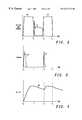
- FIG. 3is a plot that illustrates the current being supplied through the switch for charging capacitor 70 (see FIG. 1 ).
- the vertical axisrepresents a current and the horizontal axis represents time.
- current from terminal 64is supplied through transistor 36 (see FIG. 1) at times to and t 2 for charging capacitor 70 .
- Waveform 84shows a wider current pulse at time to than the current pulse at time t 2 .
- capacitor 70receives more charge at time to that at time t 2 .
- Bias supply circuit 12does not supply current through transistor 36 for charging capacitor 70 at times t 1 and t 3 .
- FIG. 4is a plot that illustrates the voltage at terminal 68 (see FIG. 1) that is generated by charging capacitor 70 .
- the vertical axisrepresents voltage and the horizontal axis represents time.
- waveform 86shows that the voltage across capacitor 70 is substantially increased between the times t 0 and t 1 , decreased between the times t 1 and t 2 , and increased again between the times t 2 and t 3 .
- diode 42is forward biased and current is supplied through transistor 36 from terminal 64 to terminal 68 and capacitor 70 .
- Waveform 86shows that the voltage at terminal 68 is increased between times t 0 and t 1 as capacitor 70 is charged.
- bias supply circuit 12allows the voltage at the gate terminal of transistor 60 to be substantially isolated from the changes in voltage at terminals 64 and 66 .
- the voltage generated at terminal 68supplies the positive operating voltage for polarity comparator 14 and driver circuit 16 .
- polarity comparator 14 and driver circuit 16provide a logic one value to the gate terminal of MOSFET 60
- the amplitude of the logic one valueis relatively constant over an accepted range of voltages received at terminal 64 .
Landscapes
- Engineering & Computer Science (AREA)
- Power Engineering (AREA)
- Rectifiers (AREA)
- Dc-Dc Converters (AREA)
Abstract
Description
Claims (15)
Priority Applications (2)
| Application Number | Priority Date | Filing Date | Title |
|---|---|---|---|
| US09/287,279US6271712B1 (en) | 1999-04-07 | 1999-04-07 | Synchronous rectifier and method of operation |
| PCT/US2000/007613WO2000060730A1 (en) | 1999-04-07 | 2000-03-22 | Synchronous rectifier and method of operation |
Applications Claiming Priority (1)
| Application Number | Priority Date | Filing Date | Title |
|---|---|---|---|
| US09/287,279US6271712B1 (en) | 1999-04-07 | 1999-04-07 | Synchronous rectifier and method of operation |
Publications (1)
| Publication Number | Publication Date |
|---|---|
| US6271712B1true US6271712B1 (en) | 2001-08-07 |
Family
ID=23102213
Family Applications (1)
| Application Number | Title | Priority Date | Filing Date |
|---|---|---|---|
| US09/287,279Expired - LifetimeUS6271712B1 (en) | 1999-04-07 | 1999-04-07 | Synchronous rectifier and method of operation |
Country Status (2)
| Country | Link |
|---|---|
| US (1) | US6271712B1 (en) |
| WO (1) | WO2000060730A1 (en) |
Cited By (27)
| Publication number | Priority date | Publication date | Assignee | Title |
|---|---|---|---|---|
| US20030030326A1 (en)* | 2001-08-10 | 2003-02-13 | Shakti Systems, Inc. | Distributed power and supply architecture |
| US20030048653A1 (en)* | 2000-03-28 | 2003-03-13 | Kazuki Watanabe | Semiconductor integrated circuit device and contactless electronic device |
| US20030048643A1 (en)* | 2001-09-13 | 2003-03-13 | Feng Lin | Method and circuit for start up in a power converter |
| US20030048648A1 (en)* | 2001-09-13 | 2003-03-13 | Feng Lin | Current sense and control of DC/DC converters |
| US20030052655A1 (en)* | 1999-07-15 | 2003-03-20 | Incep Technologies, Inc. | Integrated magnetic buck converter with magnetically coupled synchronously rectified mosfet gate drive |
| US20040037099A1 (en)* | 2002-06-27 | 2004-02-26 | Yukihiro Nishikawa | Control circuit of MOSFET for synchronous rectification |
| US6819088B2 (en) | 2001-11-05 | 2004-11-16 | Krishna Shenai | DC-DC converter with resonant gate drive |
| US20050122753A1 (en)* | 2003-11-04 | 2005-06-09 | International Rectifier Corporation | Integrated synchronous rectifier package |
| US6940703B1 (en)* | 1999-12-15 | 2005-09-06 | Tripath Technology, Inc. | Overvoltage protection circuit |
| US6992906B1 (en)* | 2002-12-10 | 2006-01-31 | Edward Herbert | Synthetic rectifiers |
| US20060076626A1 (en)* | 2004-10-13 | 2006-04-13 | Kazuki Watanabe | Semiconductor integrated circuit device, contactless electronic device, and handheld terminal |
| US20080298106A1 (en)* | 2007-05-30 | 2008-12-04 | Texas Instruments Incorporated | Adaptive rectifier Architecture and method for switching regulators |
| US20090016083A1 (en)* | 2003-11-04 | 2009-01-15 | Marco Soldano | Secondary side synchronous rectifier for resonant converter |
| DE102008031688A1 (en) | 2007-07-05 | 2009-02-19 | Infineon Technologies Austria Ag | Active diode |
| US20090184746A1 (en)* | 2008-01-22 | 2009-07-23 | Microsemi Corporation | Low Voltage Drop Unidirectional Electronic Valve |
| US20100060245A1 (en)* | 2008-09-08 | 2010-03-11 | Gm Global Technology Operations, Inc. | Rectifying circuit for a multiphase electric machine |
| US20110006232A1 (en)* | 2009-07-09 | 2011-01-13 | Microsemi Corporation | Low voltage drop closed loop unidirectional electronic valve |
| US20110096572A1 (en)* | 2009-10-28 | 2011-04-28 | Iwatt Inc. | Low power consumption start-up circuit with dynamic switching |
| WO2011067635A1 (en)* | 2009-12-04 | 2011-06-09 | Convenientpower Hk Ltd | Ac-dc converter and ac-dc conversion method |
| US20110233723A1 (en)* | 2010-03-25 | 2011-09-29 | Elpida Memory, Inc. | Dielectric film and semiconductor device |
| US8606447B2 (en) | 2011-05-23 | 2013-12-10 | GM Global Technology Operations LLC | Method and apparatus to operate a powertrain system including an electric machine having a disconnected high-voltage battery |
| US8842397B2 (en) | 2011-05-23 | 2014-09-23 | Microsemi Corporation | Photo-voltaic safety de-energizing device |
| US9013898B2 (en) | 2012-09-21 | 2015-04-21 | Semiconductor Components Industries, Llc | Synchronous rectifier controller, power converter using same, and method therefor |
| US9434258B2 (en) | 2011-11-18 | 2016-09-06 | GM Global Technology Operations LLC | Power converter with diagnostic unit power supply output |
| CN108199456A (en)* | 2018-02-26 | 2018-06-22 | 深圳市梓晶微科技有限公司 | A kind of lithium battery quick-charging circuit and charging method |
| US10333425B1 (en)* | 2018-05-03 | 2019-06-25 | Linear Technology Holding Llc | Self-biasing ideal diode circuit |
| US20230135356A1 (en)* | 2021-10-28 | 2023-05-04 | Stmicroelectronics Asia Pacific Pte Ltd | Method to maintain synchronous rectification at light loads |
Families Citing this family (3)
| Publication number | Priority date | Publication date | Assignee | Title |
|---|---|---|---|---|
| DE60144043D1 (en)* | 2000-12-04 | 2011-03-31 | Nec Tokin Corp | Balanced DC-DC converter with synchronous rectifiers and operational amplifiers in the driver stage |
| CN106936323A (en)* | 2015-12-29 | 2017-07-07 | 上海科特新材料股份有限公司 | AC-DC is without harmonic synchronous fairing |
| US10014851B2 (en) | 2016-11-02 | 2018-07-03 | Texas Instruments Incorporated | Current sensing and control for a transistor power switch |
Citations (9)
| Publication number | Priority date | Publication date | Assignee | Title |
|---|---|---|---|---|
| US4403183A (en)* | 1981-04-10 | 1983-09-06 | Tektronix, Inc. | Active voltage probe |
| US4617473A (en)* | 1984-01-03 | 1986-10-14 | Intersil, Inc. | CMOS backup power switching circuit |
| US5038266A (en)* | 1990-01-02 | 1991-08-06 | General Electric Company | High efficiency, regulated DC supply |
| US5510972A (en)* | 1994-06-29 | 1996-04-23 | Philips Electronics North America Corporation | Bridge rectifier circuit having active switches and an active control circuit |
| US5608352A (en)* | 1993-12-22 | 1997-03-04 | Kabushiki Kaisha Toshiba | Differential input circuit capable of broadening operation range of input common mode potential |
| US5703518A (en)* | 1994-08-01 | 1997-12-30 | Oki Electric Industry Co., Ltd. | Absolute value circuit capable of providing full-wave rectification with less distortion |
| US5731694A (en)* | 1993-03-23 | 1998-03-24 | Linear Technology Corporation | Control circuit and method for maintaining high efficiency over broard current ranges in a switching regulator circuit |
| US5929615A (en)* | 1998-09-22 | 1999-07-27 | Impala Linear Corporation | Step-up/step-down voltage regulator using an MOS synchronous rectifier |
| US5991182A (en)* | 1995-12-29 | 1999-11-23 | Em Microelectric -Marin Sa | Active rectifier having minimal energy losses |
Family Cites Families (10)
| Publication number | Priority date | Publication date | Assignee | Title |
|---|---|---|---|---|
| US4266189A (en)* | 1976-07-28 | 1981-05-05 | Sun Electric Corporation | Current measuring apparatus and method |
| US4417164A (en)* | 1981-06-18 | 1983-11-22 | Southern Gas Association | Mechanical valve analog |
| NZ236551A (en)* | 1990-12-19 | 1995-07-26 | Fisher & Paykel | Direct current power supply energised from current commutated through motor winding |
| IT1250301B (en)* | 1991-09-09 | 1995-04-07 | Sgs Thomson Microelectronics | LOW FALL VOLTAGE REGULATOR. |
| US5550463A (en)* | 1993-05-20 | 1996-08-27 | Coveley; Michael | Power supply connected in parallel with solid state switch for phase control of average power to a load |
| US5506527A (en)* | 1994-04-15 | 1996-04-09 | Hewlett-Packard Compnay | Low power diode |
| US5600552A (en)* | 1995-03-02 | 1997-02-04 | Heath Company | Direct current power supply for use in series with a load in an alternating current circuit |
| US5736890A (en)* | 1996-04-03 | 1998-04-07 | Semi Technology Design, Inc. | Method and apparatus for controlling transistors as rectifiers |
| SE521139C2 (en)* | 1997-03-24 | 2003-10-07 | Abb Ab | high voltage converter circuit |
| US6026005A (en)* | 1997-06-11 | 2000-02-15 | International Rectifier Corp. | Single ended forward converter with synchronous rectification and delay circuit in phase-locked loop |
- 1999
- 1999-04-07USUS09/287,279patent/US6271712B1/ennot_activeExpired - Lifetime
- 2000
- 2000-03-22WOPCT/US2000/007613patent/WO2000060730A1/enactiveApplication Filing
Patent Citations (9)
| Publication number | Priority date | Publication date | Assignee | Title |
|---|---|---|---|---|
| US4403183A (en)* | 1981-04-10 | 1983-09-06 | Tektronix, Inc. | Active voltage probe |
| US4617473A (en)* | 1984-01-03 | 1986-10-14 | Intersil, Inc. | CMOS backup power switching circuit |
| US5038266A (en)* | 1990-01-02 | 1991-08-06 | General Electric Company | High efficiency, regulated DC supply |
| US5731694A (en)* | 1993-03-23 | 1998-03-24 | Linear Technology Corporation | Control circuit and method for maintaining high efficiency over broard current ranges in a switching regulator circuit |
| US5608352A (en)* | 1993-12-22 | 1997-03-04 | Kabushiki Kaisha Toshiba | Differential input circuit capable of broadening operation range of input common mode potential |
| US5510972A (en)* | 1994-06-29 | 1996-04-23 | Philips Electronics North America Corporation | Bridge rectifier circuit having active switches and an active control circuit |
| US5703518A (en)* | 1994-08-01 | 1997-12-30 | Oki Electric Industry Co., Ltd. | Absolute value circuit capable of providing full-wave rectification with less distortion |
| US5991182A (en)* | 1995-12-29 | 1999-11-23 | Em Microelectric -Marin Sa | Active rectifier having minimal energy losses |
| US5929615A (en)* | 1998-09-22 | 1999-07-27 | Impala Linear Corporation | Step-up/step-down voltage regulator using an MOS synchronous rectifier |
Cited By (54)
| Publication number | Priority date | Publication date | Assignee | Title |
|---|---|---|---|---|
| US20030052655A1 (en)* | 1999-07-15 | 2003-03-20 | Incep Technologies, Inc. | Integrated magnetic buck converter with magnetically coupled synchronously rectified mosfet gate drive |
| US6754086B2 (en) | 1999-07-15 | 2004-06-22 | Incep Technologies, Inc. | Integrated magnetic buck converter with magnetically coupled synchronously rectified mosfet gate drive |
| US6940703B1 (en)* | 1999-12-15 | 2005-09-06 | Tripath Technology, Inc. | Overvoltage protection circuit |
| US6831378B2 (en)* | 2000-03-28 | 2004-12-14 | Renesas Technology Corp. | Semiconductor integrated circuit device and contactless electronic device |
| US20030048653A1 (en)* | 2000-03-28 | 2003-03-13 | Kazuki Watanabe | Semiconductor integrated circuit device and contactless electronic device |
| US20030030326A1 (en)* | 2001-08-10 | 2003-02-13 | Shakti Systems, Inc. | Distributed power and supply architecture |
| US20030048643A1 (en)* | 2001-09-13 | 2003-03-13 | Feng Lin | Method and circuit for start up in a power converter |
| US20030048648A1 (en)* | 2001-09-13 | 2003-03-13 | Feng Lin | Current sense and control of DC/DC converters |
| US6574124B2 (en) | 2001-09-13 | 2003-06-03 | Netpower Technologies, Inc. | Plural power converters with individual conditioned error signals shared on a current sharing bus |
| US6760235B2 (en) | 2001-09-13 | 2004-07-06 | Netpower Technologies, Inc. | Soft start for a synchronous rectifier in a power converter |
| US6819088B2 (en) | 2001-11-05 | 2004-11-16 | Krishna Shenai | DC-DC converter with resonant gate drive |
| US20040037099A1 (en)* | 2002-06-27 | 2004-02-26 | Yukihiro Nishikawa | Control circuit of MOSFET for synchronous rectification |
| US6781432B2 (en)* | 2002-06-27 | 2004-08-24 | Fuji Electric Co., Ltd. | Control circuit of MOSFET for synchronous rectification |
| US6992906B1 (en)* | 2002-12-10 | 2006-01-31 | Edward Herbert | Synthetic rectifiers |
| US20090016083A1 (en)* | 2003-11-04 | 2009-01-15 | Marco Soldano | Secondary side synchronous rectifier for resonant converter |
| US7768808B2 (en) | 2003-11-04 | 2010-08-03 | International Rectifier Corporation | Integrated synchronous rectifier package |
| US20050122753A1 (en)* | 2003-11-04 | 2005-06-09 | International Rectifier Corporation | Integrated synchronous rectifier package |
| US7408796B2 (en) | 2003-11-04 | 2008-08-05 | International Rectifier Corporation | Integrated synchronous rectifier package |
| US20080247209A1 (en)* | 2003-11-04 | 2008-10-09 | International Rectifier Corporation | Integrated synchronous rectifier package |
| US8134851B2 (en) | 2003-11-04 | 2012-03-13 | International Rectifier Corporation | Secondary side synchronous rectifier for resonant converter |
| US20060076626A1 (en)* | 2004-10-13 | 2006-04-13 | Kazuki Watanabe | Semiconductor integrated circuit device, contactless electronic device, and handheld terminal |
| CN100589314C (en)* | 2004-10-13 | 2010-02-10 | 株式会社瑞萨科技 | Semiconductor integrated circuits, non-contact electronic devices and portable information terminals |
| US7245513B2 (en)* | 2004-10-13 | 2007-07-17 | Renesas Technology Corp. | Semiconductor integrated circuit device, contactless electronic device, and handheld terminal |
| WO2008150976A3 (en)* | 2007-05-30 | 2009-02-26 | Texas Instruments Inc | Adaptive rectifier architecture and method for switching regulators |
| US20080298106A1 (en)* | 2007-05-30 | 2008-12-04 | Texas Instruments Incorporated | Adaptive rectifier Architecture and method for switching regulators |
| US8278889B2 (en) | 2007-05-30 | 2012-10-02 | Texas Instruments Incorporated | Adaptive rectifier architecture and method for switching regulators |
| DE102008031688A1 (en) | 2007-07-05 | 2009-02-19 | Infineon Technologies Austria Ag | Active diode |
| US20090184746A1 (en)* | 2008-01-22 | 2009-07-23 | Microsemi Corporation | Low Voltage Drop Unidirectional Electronic Valve |
| US20100060245A1 (en)* | 2008-09-08 | 2010-03-11 | Gm Global Technology Operations, Inc. | Rectifying circuit for a multiphase electric machine |
| US8064227B2 (en) | 2008-09-08 | 2011-11-22 | GM Global Technology Operations LLC | Rectifying circuit for a multiphase electric machine |
| CN102473740B (en)* | 2009-07-09 | 2015-04-08 | 美高森美公司 | Low voltage drop closed loop unidirectional electronic valve |
| US20110006232A1 (en)* | 2009-07-09 | 2011-01-13 | Microsemi Corporation | Low voltage drop closed loop unidirectional electronic valve |
| US8169252B2 (en) | 2009-07-09 | 2012-05-01 | Microsemi Corporation | Low voltage drop closed loop unidirectional electronic valve |
| CN102473740A (en)* | 2009-07-09 | 2012-05-23 | 美高森美公司 | Low voltage drop closed loop one-way electronic valve |
| US8581568B2 (en)* | 2009-10-28 | 2013-11-12 | Iwatt Inc. | Low power consumption start-up circuit with dynamic switching |
| US20110096572A1 (en)* | 2009-10-28 | 2011-04-28 | Iwatt Inc. | Low power consumption start-up circuit with dynamic switching |
| WO2011067635A1 (en)* | 2009-12-04 | 2011-06-09 | Convenientpower Hk Ltd | Ac-dc converter and ac-dc conversion method |
| US20110134673A1 (en)* | 2009-12-04 | 2011-06-09 | Convenientpower Hk Ltd | Ac-dc converter and ac-dc conversion method |
| US8300440B2 (en) | 2009-12-04 | 2012-10-30 | ConvenientPower HK Ltd. | AC-DC converter and AC-DC conversion method |
| US20110233723A1 (en)* | 2010-03-25 | 2011-09-29 | Elpida Memory, Inc. | Dielectric film and semiconductor device |
| US8842397B2 (en) | 2011-05-23 | 2014-09-23 | Microsemi Corporation | Photo-voltaic safety de-energizing device |
| US8606447B2 (en) | 2011-05-23 | 2013-12-10 | GM Global Technology Operations LLC | Method and apparatus to operate a powertrain system including an electric machine having a disconnected high-voltage battery |
| US9434258B2 (en) | 2011-11-18 | 2016-09-06 | GM Global Technology Operations LLC | Power converter with diagnostic unit power supply output |
| US9013898B2 (en) | 2012-09-21 | 2015-04-21 | Semiconductor Components Industries, Llc | Synchronous rectifier controller, power converter using same, and method therefor |
| CN108199456B (en)* | 2018-02-26 | 2024-01-05 | 深圳市梓晶微科技有限公司 | Quick charging circuit and charging method for lithium battery |
| CN108199456A (en)* | 2018-02-26 | 2018-06-22 | 深圳市梓晶微科技有限公司 | A kind of lithium battery quick-charging circuit and charging method |
| US10333425B1 (en)* | 2018-05-03 | 2019-06-25 | Linear Technology Holding Llc | Self-biasing ideal diode circuit |
| CN112075024A (en)* | 2018-05-03 | 2020-12-11 | 亚德诺半导体国际无限责任公司 | Self-biased ideal diode circuit |
| JP2021520774A (en)* | 2018-05-03 | 2021-08-19 | アナログ・ディヴァイシス・インターナショナル・アンリミテッド・カンパニー | Self-bias ideal diode circuit |
| US11557981B2 (en) | 2018-05-03 | 2023-01-17 | Analog Devices International Unlimited Company | Self-biasing ideal diode circuit |
| EP4181396A1 (en)* | 2018-05-03 | 2023-05-17 | Analog Devices International Unlimited Company | Self-biasing ideal diode circuit |
| WO2019212828A1 (en)* | 2018-05-03 | 2019-11-07 | Linear Technology Holding Llc | Self-biasing ideal diode circuit |
| CN112075024B (en)* | 2018-05-03 | 2024-09-24 | 亚德诺半导体国际无限责任公司 | Self-biasing ideal diode circuit |
| US20230135356A1 (en)* | 2021-10-28 | 2023-05-04 | Stmicroelectronics Asia Pacific Pte Ltd | Method to maintain synchronous rectification at light loads |
Also Published As
| Publication number | Publication date |
|---|---|
| WO2000060730A1 (en) | 2000-10-12 |
Similar Documents
| Publication | Publication Date | Title |
|---|---|---|
| US6271712B1 (en) | Synchronous rectifier and method of operation | |
| CN102570782B (en) | For the system and method for bootstrapped switch driver | |
| US6269012B1 (en) | Energy efficient power supply with light-load detection | |
| CN108206634B (en) | Insulating synchronous rectification DC/DC converter, controller, adapter and equipment | |
| US11502685B2 (en) | Gate drive circuit and control circuit for switching circuit, and switching power supply | |
| JPWO2005034324A1 (en) | Switching power supply | |
| US11588410B2 (en) | Switched mode power supplies with configurable communication addresses | |
| CN102480217A (en) | System and method for actuating a switch | |
| US10985748B2 (en) | Drive voltage booster | |
| CN102480216B (en) | System and method for driving acascode switch | |
| JP2009515501A (en) | Method and circuit device for controlling semiconductor switch with galvanic isolation | |
| US20210234454A1 (en) | Drive circuit and power conversion device | |
| US7248093B2 (en) | Bipolar bootstrap top switch gate drive for half-bridge semiconductor power topologies | |
| EP0865161B1 (en) | Driving apparatus for an inductive load | |
| JPH08289538A (en) | Dc-dc converter | |
| TW202130102A (en) | Method and apparatus for generating control signal and charging dc supply in a secondary synchronous rectifier | |
| US12348124B2 (en) | Bootstrap device and buck-boost converter | |
| KR101091922B1 (en) | Inverter driver and lamp driver including the same, and driving method thereof | |
| JP7426397B2 (en) | Power electronic devices and methods for supplying voltage to drive circuits of power semiconductor switches | |
| US6469567B1 (en) | Power supply circuit and method | |
| JP3756353B2 (en) | Semiconductor device drive circuit | |
| KR102393664B1 (en) | Inverter switch gate driver and inverter | |
| US12381473B2 (en) | Driver circuit for a power transistor | |
| US20240372480A1 (en) | Multi-synchronous rectifier (sr) drive switching control system | |
| JP2002119058A (en) | Multiple-output, synchronous-rectification, switching power supply |
Legal Events
| Date | Code | Title | Description |
|---|---|---|---|
| AS | Assignment | Owner name:MOTOROLA, INC., ILLINOIS Free format text:ASSIGNMENT OF ASSIGNORS INTEREST;ASSIGNOR:BALL, ALAN RICHARD;REEL/FRAME:009908/0736 Effective date:19990330 | |
| AS | Assignment | Owner name:SEMICONDUCTOR COMPONENTS INDUSTRIES, LLC, ARIZONA Free format text:ASSIGNMENT OF ASSIGNORS INTEREST;ASSIGNOR:MOTOROLA, INC.;REEL/FRAME:010776/0122 Effective date:20000414 | |
| STCF | Information on status: patent grant | Free format text:PATENTED CASE | |
| AS | Assignment | Owner name:JPMORGAN CHASE BANK, AS COLLATERAL AGENT, NEW YORK Free format text:SUPPLEMENT TO SECURITY AGREEMENT;ASSIGNORS:SEMICONDUCTOR COMPONENTS INDUSTRIES, LLC;SEMICONDUCTOR COMPONENTS OF RHODE ISLAND, INC.;REEL/FRAME:012991/0180 Effective date:20020505 | |
| AS | Assignment | Owner name:WELLS FARGO BANK MINNESOTA, NATIONAL ASSOCIATION, Free format text:SECURITY AGREEMENT;ASSIGNORS:SEMICONDUCTOR COMPONENTS INDUSTRIES, LLC;SEMICONDUCTOR COMPONENTS INDUSTRIES OF RHODE ISLAND, INC.;REEL/FRAME:012958/0638 Effective date:20020506 | |
| AS | Assignment | Owner name:JPMORGAN CHASE BANK, NEW YORK Free format text:SECURITY INTEREST;ASSIGNOR:SEMICONDUCTOR COMPONENTS INDUSTRIES, LLC;REEL/FRAME:014007/0239 Effective date:20030303 | |
| FPAY | Fee payment | Year of fee payment:4 | |
| FPAY | Fee payment | Year of fee payment:8 | |
| FPAY | Fee payment | Year of fee payment:12 | |
| AS | Assignment | Owner name:DEUTSCHE BANK AG NEW YORK BRANCH, NEW YORK Free format text:SECURITY INTEREST;ASSIGNOR:SEMICONDUCTOR COMPONENTS INDUSTRIES, LLC;REEL/FRAME:038620/0087 Effective date:20160415 | |
| AS | Assignment | Owner name:SEMICONDUCTOR COMPONENTS INDUSTRIES, LLC, ARIZONA Free format text:RELEASE BY SECURED PARTY;ASSIGNOR:WELLS FARGO BANK MINNESOTA, NATIONAL ASSOCIATION, AS COLLATERAL AGENT;REEL/FRAME:038543/0039 Effective date:20050217 | |
| AS | Assignment | Owner name:SEMICONDUCTOR COMPONENTS INDUSTRIES, LLC, ARIZONA Free format text:RELEASE BY SECURED PARTY;ASSIGNOR:JPMORGAN CHASE BANK, N.A., AS ADMINISTRATIVE AGENT AND COLLATERAL AGENT;REEL/FRAME:038631/0345 Effective date:20100511 Owner name:SEMICONDUCTOR COMPONENTS INDUSTRIES, LLC, ARIZONA Free format text:RELEASE BY SECURED PARTY;ASSIGNOR:JPMORGAN CHASE BANK, N.A. (ON ITS BEHALF AND ON BEHALF OF ITS PREDECESSOR IN INTEREST, CHASE MANHATTAN BANK);REEL/FRAME:038632/0074 Effective date:20160415 | |
| AS | Assignment | Owner name:DEUTSCHE BANK AG NEW YORK BRANCH, AS COLLATERAL AG Free format text:CORRECTIVE ASSIGNMENT TO CORRECT THE INCORRECT PATENT NUMBER 5859768 AND TO RECITE COLLATERAL AGENT ROLE OF RECEIVING PARTY IN THE SECURITY INTEREST PREVIOUSLY RECORDED ON REEL 038620 FRAME 0087. ASSIGNOR(S) HEREBY CONFIRMS THE SECURITY INTEREST;ASSIGNOR:SEMICONDUCTOR COMPONENTS INDUSTRIES, LLC;REEL/FRAME:039853/0001 Effective date:20160415 Owner name:DEUTSCHE BANK AG NEW YORK BRANCH, AS COLLATERAL AGENT, NEW YORK Free format text:CORRECTIVE ASSIGNMENT TO CORRECT THE INCORRECT PATENT NUMBER 5859768 AND TO RECITE COLLATERAL AGENT ROLE OF RECEIVING PARTY IN THE SECURITY INTEREST PREVIOUSLY RECORDED ON REEL 038620 FRAME 0087. ASSIGNOR(S) HEREBY CONFIRMS THE SECURITY INTEREST;ASSIGNOR:SEMICONDUCTOR COMPONENTS INDUSTRIES, LLC;REEL/FRAME:039853/0001 Effective date:20160415 | |
| AS | Assignment | Owner name:FAIRCHILD SEMICONDUCTOR CORPORATION, ARIZONA Free format text:RELEASE OF SECURITY INTEREST IN PATENTS RECORDED AT REEL 038620, FRAME 0087;ASSIGNOR:DEUTSCHE BANK AG NEW YORK BRANCH, AS COLLATERAL AGENT;REEL/FRAME:064070/0001 Effective date:20230622 Owner name:SEMICONDUCTOR COMPONENTS INDUSTRIES, LLC, ARIZONA Free format text:RELEASE OF SECURITY INTEREST IN PATENTS RECORDED AT REEL 038620, FRAME 0087;ASSIGNOR:DEUTSCHE BANK AG NEW YORK BRANCH, AS COLLATERAL AGENT;REEL/FRAME:064070/0001 Effective date:20230622 |