US6271148B1 - Method for improved remote microwave plasma source for use with substrate processing system - Google Patents
Method for improved remote microwave plasma source for use with substrate processing systemDownload PDFInfo
- Publication number
- US6271148B1 US6271148B1US09/416,861US41686199AUS6271148B1US 6271148 B1US6271148 B1US 6271148B1US 41686199 AUS41686199 AUS 41686199AUS 6271148 B1US6271148 B1US 6271148B1
- Authority
- US
- United States
- Prior art keywords
- applicator
- plasma
- chamber
- microwave
- gas
- Prior art date
- Legal status (The legal status is an assumption and is not a legal conclusion. Google has not performed a legal analysis and makes no representation as to the accuracy of the status listed.)
- Expired - Fee Related
Links
Images


Classifications
- C—CHEMISTRY; METALLURGY
- C23—COATING METALLIC MATERIAL; COATING MATERIAL WITH METALLIC MATERIAL; CHEMICAL SURFACE TREATMENT; DIFFUSION TREATMENT OF METALLIC MATERIAL; COATING BY VACUUM EVAPORATION, BY SPUTTERING, BY ION IMPLANTATION OR BY CHEMICAL VAPOUR DEPOSITION, IN GENERAL; INHIBITING CORROSION OF METALLIC MATERIAL OR INCRUSTATION IN GENERAL
- C23C—COATING METALLIC MATERIAL; COATING MATERIAL WITH METALLIC MATERIAL; SURFACE TREATMENT OF METALLIC MATERIAL BY DIFFUSION INTO THE SURFACE, BY CHEMICAL CONVERSION OR SUBSTITUTION; COATING BY VACUUM EVAPORATION, BY SPUTTERING, BY ION IMPLANTATION OR BY CHEMICAL VAPOUR DEPOSITION, IN GENERAL
- C23C16/00—Chemical coating by decomposition of gaseous compounds, without leaving reaction products of surface material in the coating, i.e. chemical vapour deposition [CVD] processes
- C23C16/44—Chemical coating by decomposition of gaseous compounds, without leaving reaction products of surface material in the coating, i.e. chemical vapour deposition [CVD] processes characterised by the method of coating
- C23C16/52—Controlling or regulating the coating process
- C—CHEMISTRY; METALLURGY
- C23—COATING METALLIC MATERIAL; COATING MATERIAL WITH METALLIC MATERIAL; CHEMICAL SURFACE TREATMENT; DIFFUSION TREATMENT OF METALLIC MATERIAL; COATING BY VACUUM EVAPORATION, BY SPUTTERING, BY ION IMPLANTATION OR BY CHEMICAL VAPOUR DEPOSITION, IN GENERAL; INHIBITING CORROSION OF METALLIC MATERIAL OR INCRUSTATION IN GENERAL
- C23C—COATING METALLIC MATERIAL; COATING MATERIAL WITH METALLIC MATERIAL; SURFACE TREATMENT OF METALLIC MATERIAL BY DIFFUSION INTO THE SURFACE, BY CHEMICAL CONVERSION OR SUBSTITUTION; COATING BY VACUUM EVAPORATION, BY SPUTTERING, BY ION IMPLANTATION OR BY CHEMICAL VAPOUR DEPOSITION, IN GENERAL
- C23C16/00—Chemical coating by decomposition of gaseous compounds, without leaving reaction products of surface material in the coating, i.e. chemical vapour deposition [CVD] processes
- C23C16/44—Chemical coating by decomposition of gaseous compounds, without leaving reaction products of surface material in the coating, i.e. chemical vapour deposition [CVD] processes characterised by the method of coating
- C23C16/4401—Means for minimising impurities, e.g. dust, moisture or residual gas, in the reaction chamber
- C23C16/4405—Cleaning of reactor or parts inside the reactor by using reactive gases
- C—CHEMISTRY; METALLURGY
- C23—COATING METALLIC MATERIAL; COATING MATERIAL WITH METALLIC MATERIAL; CHEMICAL SURFACE TREATMENT; DIFFUSION TREATMENT OF METALLIC MATERIAL; COATING BY VACUUM EVAPORATION, BY SPUTTERING, BY ION IMPLANTATION OR BY CHEMICAL VAPOUR DEPOSITION, IN GENERAL; INHIBITING CORROSION OF METALLIC MATERIAL OR INCRUSTATION IN GENERAL
- C23C—COATING METALLIC MATERIAL; COATING MATERIAL WITH METALLIC MATERIAL; SURFACE TREATMENT OF METALLIC MATERIAL BY DIFFUSION INTO THE SURFACE, BY CHEMICAL CONVERSION OR SUBSTITUTION; COATING BY VACUUM EVAPORATION, BY SPUTTERING, BY ION IMPLANTATION OR BY CHEMICAL VAPOUR DEPOSITION, IN GENERAL
- C23C16/00—Chemical coating by decomposition of gaseous compounds, without leaving reaction products of surface material in the coating, i.e. chemical vapour deposition [CVD] processes
- C23C16/44—Chemical coating by decomposition of gaseous compounds, without leaving reaction products of surface material in the coating, i.e. chemical vapour deposition [CVD] processes characterised by the method of coating
- C23C16/448—Chemical coating by decomposition of gaseous compounds, without leaving reaction products of surface material in the coating, i.e. chemical vapour deposition [CVD] processes characterised by the method of coating characterised by the method used for generating reactive gas streams, e.g. by evaporation or sublimation of precursor materials
- C23C16/452—Chemical coating by decomposition of gaseous compounds, without leaving reaction products of surface material in the coating, i.e. chemical vapour deposition [CVD] processes characterised by the method of coating characterised by the method used for generating reactive gas streams, e.g. by evaporation or sublimation of precursor materials by activating reactive gas streams before their introduction into the reaction chamber, e.g. by ionisation or addition of reactive species
- H—ELECTRICITY
- H01—ELECTRIC ELEMENTS
- H01J—ELECTRIC DISCHARGE TUBES OR DISCHARGE LAMPS
- H01J37/00—Discharge tubes with provision for introducing objects or material to be exposed to the discharge, e.g. for the purpose of examination or processing thereof
- H01J37/32—Gas-filled discharge tubes
- H01J37/32009—Arrangements for generation of plasma specially adapted for examination or treatment of objects, e.g. plasma sources
- H01J37/32192—Microwave generated discharge
- H—ELECTRICITY
- H01—ELECTRIC ELEMENTS
- H01J—ELECTRIC DISCHARGE TUBES OR DISCHARGE LAMPS
- H01J37/00—Discharge tubes with provision for introducing objects or material to be exposed to the discharge, e.g. for the purpose of examination or processing thereof
- H01J37/32—Gas-filled discharge tubes
- H01J37/32009—Arrangements for generation of plasma specially adapted for examination or treatment of objects, e.g. plasma sources
- H01J37/32357—Generation remote from the workpiece, e.g. down-stream
- H—ELECTRICITY
- H01—ELECTRIC ELEMENTS
- H01J—ELECTRIC DISCHARGE TUBES OR DISCHARGE LAMPS
- H01J37/00—Discharge tubes with provision for introducing objects or material to be exposed to the discharge, e.g. for the purpose of examination or processing thereof
- H01J37/32—Gas-filled discharge tubes
- H01J37/32431—Constructional details of the reactor
- H01J37/32798—Further details of plasma apparatus not provided for in groups H01J37/3244 - H01J37/32788; special provisions for cleaning or maintenance of the apparatus
- H01J37/32853—Hygiene
- H01J37/32862—In situ cleaning of vessels and/or internal parts
- H—ELECTRICITY
- H01—ELECTRIC ELEMENTS
- H01L—SEMICONDUCTOR DEVICES NOT COVERED BY CLASS H10
- H01L21/00—Processes or apparatus adapted for the manufacture or treatment of semiconductor or solid state devices or of parts thereof
- H01L21/67—Apparatus specially adapted for handling semiconductor or electric solid state devices during manufacture or treatment thereof; Apparatus specially adapted for handling wafers during manufacture or treatment of semiconductor or electric solid state devices or components ; Apparatus not specifically provided for elsewhere
- H01L21/67005—Apparatus not specifically provided for elsewhere
- H01L21/67011—Apparatus for manufacture or treatment
- H01L21/67017—Apparatus for fluid treatment
- H01L21/67028—Apparatus for fluid treatment for cleaning followed by drying, rinsing, stripping, blasting or the like
Definitions
- the present inventionrelates to substrate processing. More specifically, the present invention relates to apparatus and methods for upgrading a substrate processing system. Some embodiments of the present invention are particularly useful for cleaning a chamber in a substrate processing system. However, other embodiments of the present invention also may be useful for etching or depositing films on a substrate processed in the substrate processing system.
- a layersuch as a metal silicide layer like tungsten silicide (WSi x ), on a substrate or wafer.
- a layercan be deposited by chemical vapor deposition (CVD).
- CVDchemical vapor deposition
- reactive gasesare supplied to the substrate surface where heat-induced chemical reactions take place to form the desired film over the surface of the substrate being processed.
- PECVDplasma-enhanced CVD
- RFradio frequency
- the heater and other process kit partscan be removed and replaced to remove unwanted accumulations in the CVD system.
- the cost of maintaining the substrate processing systemcan become very high.
- a reactive plasma cleaningis regularly performed in situ in the processing chamber to remove the unwanted deposition material from the chamber walls, heater, and other process kit parts of the processing chamber. Commonly performed between deposition steps for every wafer or every n wafers, this cleaning procedure is performed as a standard chamber cleaning operation where the etching gas is used to remove or etch the unwanted deposited material.
- Common etching techniquesinclude plasma CVD techniques that promote excitation and/or disassociation of the reactant gases by the application of RF energy with capacitively-coupled electrodes to a reaction zone proximate the substrate surface. In these techniques, a plasma of highly reactive species is created that reacts with and etches away the unwanted deposition material from the chamber walls and other areas.
- etching gases useful for etching unwanted metalare often corrosive and attack the materials which make up the chamber, heater, and process kit parts of the processing chamber.
- use of in situ plasma cleaningalso causes ion bombardment of the metallic parts of the CVD apparatus, causing physical damage to the gas distribution manifold and the inside chamber walls. Therefore, in situ cleaning with these etching gases may make it difficult to effectively clean excess CVD film without also eventually damaging the heater and other chamber parts in the cleaning process.
- maintaining chamber performancemay result in damage to expensive consumable items which need frequent replacement as a result.
- a second cleaning procedure(often referred to as a preventive maintenance cleaning) involves opening the processing chamber and physically wiping the entire reactor—including the chamber walls, exhaust and other areas having accumulated residue—with a special cloth and cleaning fluids. Without these frequent cleaning procedures, impurities from the build up in the CVD apparatus can migrate onto the wafer and cause device damage. Thus, properly cleaning CVD apparatus is important for the smooth operation of substrate processing, improved device yield and better, product performance.
- FIG. 5illustrates an exemplary remote microwave plasma system according to the prior art.
- the remote microwave plasma systemincludes a ceramic plasma applicator tube 601 , a conventional magnetron 603 (coupled to a power source, not shown) with an antenna 604 , isolator (not shown), ultra-violet (UV) lamp 605 with power supply 607 , and bulky waveguide system 609 with tuning assembly (not shown).
- Ceramic applicator tube 601includes a gas inlet 613 connected to a gas source (not shown) for introduction of a reactive gas into the tube 601 , where microwaves passing through the portion of tube 301 disposed within a portion of waveguide 611 radiate the reactive gas, which is ignited by UV lamp 605 to form a plasma in a space 613 . Radicals exit an outlet 615 of ceramic tube 601 that is connected to a downstream processing chamber.
- Such conventional remote microwave plasma systemsproduce plasma in the relatively small physical space 613 (for example, about a two-inch lengthwise section of a ceramic applicator tube having about a 1 inch diameter) in the ceramic applicator tube 601 , having a total length of about 18-24 inches, which is disposed through a portion of the waveguide 611 in waveguide system 609 .
- the plasma formed in this small space 613 of the ceramic applicator tube 601 by magnetrons using high power supplieshas a high plasma density and requires expensive, high power density, direct current (DC) microwave power supplies in order to obtain sufficiently high microwave coupling efficiency. Since the plasma formed in small space 613 has such a high plasma density, the ceramic applicator tube 601 often becomes very hot.
- Such ceramic applicator tubeswhich are subject to cracking and breakage after repeated thermal cycling, can be expensive to replace. Additionally, some of these conventional remote plasma sources may require a UV lamp or a microwave source with very high wattage (on the order of 3 kilowatts (kW)) in order to ignite the plasma.
- the present inventionprovides an apparatus for an improved remote microwave plasma system for use with a downstream substrate processing system.
- the apparatusprovides a microwave-generated plasma that may be used to provide efficient cleaning of the downstream substrate processing system, according to a specific embodiment. Etching or depositing a layer onto a substrate in the downstream substrate processing system may also be achieved using the apparatus of the present invention according to other embodiments.
- the present inventionprovides an efficient, robust, relatively inexpensive microwave plasma system as a retrofit for or a removable addition onto existing substrate processing apparatus.
- the present inventionprovides an improved substrate processing apparatus or retrofit of existing apparatus capable of efficiently cleaning the substrate processing apparatus.
- the present inventionprovides apparatus for a remote microwave plasma system for use with a substrate processing apparatus.
- the apparatusincludes a plasma applicator defining a volume.
- the plasma applicatorincludes a conductive applicator body, a first end wall and a second end wall opposite the first end wall.
- the first end wallincludes a microwave-transparent plate.
- the plasma applicatorfurther includes a gas inlet for receiving a reactive gas into all of the volume of the plasma applicator.
- the plasma applicatoralso includes an outlet.
- the plasma applicatorreceives, through the microwave-transparent plate, microwaves that form a plasma in the volume from the reactive gas energized by the microwaves in the plasma applicator to discharge via the outlet radicals from the plasma for use in a substrate processing apparatus located downstream from the apparatus.
- the present inventionprovides an improved substrate processing system.
- This systemincludes a processing chamber, a gas delivery system configured to deliver a reactive gas to the processing chamber, and a heating system including a pedestal in the processing chamber that is for holding a substrate and heating to a selected temperature.
- the improved substrate processing systemalso includes a vacuum system configured to set and maintain a selected pressure within the processing chamber.
- the remote microwave plasma systemincludes a conductive plasma applicator defining an internal volume.
- the applicatorincludes a first end wall, a conductive second end wall opposite the first end wall, a gas inlet and an outlet.
- the first end wallincludes a microwave-transparent plate.
- the gas inlet and the outletare equipped with microwave arrestors according to a specific embodiment.
- the gas inletis for receiving a reactive gas into the internal volume of the plasma applicator.
- the microwave systemis coupled to a flanged microwave-transparent plate forming part of the first end wall.
- the internal volumeis for containing microwaves introduced through the microwave-transparent plate, and the microwaves ignite and maintain a plasma from the reactive gas. Radicals formed from the plasma exit the outlet of the plasma applicator to enter the processing chamber.
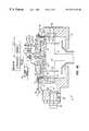
- FIGS. 1A and 1Bare vertical, cross-sectional views of one embodiment of an exemplary substrate processing apparatus, such as a CVD apparatus, which may be used in accordance with the present invention
- FIGS. 1C and 1Dare exploded perspective views of parts of the CVD chamber depicted in FIG. 1A;
- FIG. 1Eis a simplified diagram of system monitor and CVD system 10 in a system which may include one or more chambers;
- FIG. 1Fshows an illustrative block diagram of the hierarchical control structure of the system control software, computer program 70 , according to a specific embodiment
- FIG. 2Ais a simplified cross-sectional view of a semiconductor device manufactured in accordance with a specific embodiment of the present invention.
- FIGS. 2B and 2Care simplified cross-sectional views of integrated circuit structures that incorporate WSi x layers in accordance with a specific embodiment of the present invention
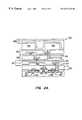
- FIG. 3Ais a cross-sectional side lengthwise view of a remote microwave plasma source module 300 according to a specific embodiment of the present invention.
- FIG. 3Bis a cross-sectional side transverse plane view along line A-A′ of one embodiment of module 300 of FIG. 3A utilizing a rectangular plasma applicator, according to one embodiment of the present invention
- FIG. 3Cis a cross-sectional side transverse plane view along line A-A′ of another embodiment of module 300 of FIG. 3A utilizing a cylindrical plasma applicator, according to another embodiment of the present invention
- FIG. 3Dis a cross-sectional side lengthwise view of a remote microwave plasma source module 300 according to another specific embodiment of the present invention.
- FIG. 4Ais a cross-sectional side lengthwise view of a cylindrical plasma applicator used in an embodiment of module 300 , according to a specific embodiment of the present invention
- FIG. 4Bis a plane view of one end of the cylindrical plasma applicator shown in FIG. 4A, according to the specific embodiment of the present invention.
- FIGS. 4Cis a plane view of the other end of the cylindrical plasma applicator shown in FIG. 4A, according to the specific embodiment of the present invention.
- FIG. 5illustrates an exemplary remote microwave plasma system according to the prior art.
- FIGS. 1A and 1Bare vertical, cross-sectional views of a CVD system 10 , having a vacuum or processing chamber 15 that includes a chamber wall 15 a and chamber lid assembly 15 b .
- Chamber wall 15 a and chamber lid assembly 15 bare shown in exploded, perspective views in FIGS. 1C and 1D.
- Reactor 10contains a gas distribution manifold 11 for dispersing process gases to a substrate (not shown) that rests on a resistively-heated pedestal 12 centered within the process chamber.
- the substratee.g. a semiconductor wafer
- the substrateis positioned on a flat (or slightly convex) surface 12 a of pedestal 12 .
- pedestal 12can be moved controllably between a lower loading/off-loading position (depicted in FIG. 1A) and an upper processing position (indicated by dashed line 14 in FIG. 1 A and shown in FIG. 1 B), which is closely adjacent to manifold 11 .
- a centerboard(not shown) includes sensors for providing information on the position of the wafers.
- Deposition and carrier gasesare introduced into chamber 15 through perforated holes 13 b (FIG. 1D) of a conventional flat, circular gas distribution face plate 13 a . More specifically, deposition process gases flow (indicated by arrow 40 in FIG. 1B) into the chamber through the inlet manifold 11 , through a conventional perforated blocker plate 42 and then through holes 13 b in gas distribution faceplate 13 a.
- deposition and carrier gasesare input from gas sources 7 through gas supply lines 8 (FIG. 1B) into a gas mixing block or system 9 where they are combined and then sent to manifold 11 . It is also possible, and desirable in some instances, to direct deposition and carrier gases directly from supply lines 8 to manifold 11 . In such a case, gas mixing system 9 is bypassed. In other situations, any of gas lines 8 may bypass gas mixing system 9 and introduce gases through passages (not shown) in the bottom of chamber 12 . As shown in FIG. 1B, there are three gas supply lines 8 in a specific embodiment to deposit WSi x .
- a first line 8 asupplies a silicon-containing gas (e.g., dichlorosilane (SiH 2 Cl 2 ) referred to as “DCS” from a DCS source from gas source 7 a ) into gas mixing system 9
- a second line 8 bsupplies a tungsten-containing gas (e.g., tungsten hexafluoride (WF 6 ) from a WF 6 source from gas source 7 b ) into gas mixing system 9
- a silicon-containing gase.g., dichlorosilane (SiH 2 Cl 2 ) referred to as “DCS” from a DCS source from gas source 7 a
- a second line 8 bsupplies a tungsten-containing gas (e.g., tungsten hexafluoride (WF 6 ) from a WF 6 source from gas source 7 b ) into gas mixing system 9
- WF 6tungsten hexafluoride
- a carrier gase.g., argon from argon sources in gas sources 7 a and 7 b
- a carrier gase.g., argon from argon sources in gas sources 7 a and 7 b
- a carrier gase.g., argon from argon sources in gas sources 7 a and 7 b
- Such mixing of gases (DCS and WF 6 upstream of chamber 15is believed to result in more uniform gas distribution into the chamber, thereby resulting in greater uniformity in the deposited WSi x film.
- a third supply line 8 cintroduces an inert purge gas (e.g., argon from a gas source 7 c ) from the bottom of the chamber to keep deposition gases away from the area of the chamber below heater 12 .
- an additional silicon sourcee.g., silane (SiH 4 ) from source 7 a may be supplied to gas line 8 a.
- the supply line for each process gasincludes (i) several safety shut-off valves (not shown) that can be used to automatically or manually shut off the flow of process gas into the chamber, and (ii) mass flow controllers (MFCs) (also not shown) that measure the flow of gas through the supply line.
- MFCsmass flow controllers
- the several safety shut-off valvesare positioned on each gas supply line in conventional configurations.
- the deposition process performed in reactor 10can be either a thermal process or a plasma-enhanced process.
- an RF power supply 44applies electrical power between the gas distribution faceplate 13 a and pedestal 12 to excite the process gas mixture to form a plasma within the cylindrical region between the faceplate 13 a and pedestal 12 .
- This regionwill be referred to herein as the “reaction region”. Constituents of the plasma react to deposit a desired film on the surface of the semiconductor wafer supported on pedestal 12 .
- RF power supply 44can be a mixed frequency RF power supply that typically supplies power at a high RF frequency (RF 1 ) of 13.56 Megahertz (MHz) and at a low RF frequency (RF 2 ) of 360 kilohertz (kHz) to enhance the decomposition of reactive species introduced into the vacuum chamber 15 .
- RF power supply 44can supply either single- or mixed-frequency RF power (or other desired variations) to manifold 11 to enhance the decomposition of reactive species introduced into chamber 15 .
- RF power supply 44is not utilized, and the process gas mixture thermally reacts to deposit the desired film on the surface of the semiconductor wafer supported on pedestal 12 , which is resistively heated to provide the thermal energy needed for the reaction.
- the plasmaheats the entire reactor 10 , including the walls of the chamber body 15 a surrounding the exhaust passageway 23 and the shut-off valve 24 .
- heated pedestal 12causes heating of reactor 10 .
- a hot liquidis circulated through the walls 15 a of reactor 10 to maintain the chamber at an elevated temperature.
- Fluids used to heat the chamber walls 15 ainclude the typical fluid types, i.e., water-based ethylene glycol or oil-based thermal transfer fluids. This heating beneficially reduces or eliminates condensation of undesirable reactant products and improves the elimination of volatile products of the process gases and contaminants that might otherwise condense on the walls of cool vacuum passages and migrate back into the processing chamber during periods of no gas flow.
- the remainder of the gas mixture that is not deposited in a layer, including reaction products,is evacuated from the chamber by a vacuum pump (not shown). Specifically, the gases are exhausted through an annular, slot-shaped orifice 16 surrounding the reaction region and into an annular exhaust plenum 17 .
- the annular slot 16 and the plenum 17are defined by the gap between the top of the chamber's cylindrical side wall 15 a (including the upper dielectric lining 19 on the wall) and the bottom of the circular chamber lid 20 .
- the 360° circular symmetry and uniformity of the slot orifice 16 and the plenum 17are important to achieving a uniform flow of process gases over the wafer so as to deposit a uniform film on the wafer.
- the wafer support platter of resistively-heated pedestal 12is heated using an embedded singleloop embedded heater element configured to make two full turns in the form of parallel concentric circles.
- An outer portion of the heater elementruns adjacent to a perimeter of the support platter, while an inner portion runs on the path of a concentric circle having a smaller radius.
- the wiring to the heater elementpasses through the stem of pedestal 12 .
- Pedestal 12may be made of material including aluminum, ceramic, or some combination thereof.
- any or all of the chamber lining, gas inlet manifold faceplate, and various other reactor hardwareare made out of material such as aluminum, anodized aluminum, or ceramic.
- An example of such CVD apparatusis described in commonly assigned U.S. Pat. No. 5,558,717 entitled “CVD Processing Chamber,” issued to Zhao et al., hereby incorporated by reference in its entirety.
- a lift mechanism and motor 32raises and lowers the heater pedestal assembly 12 and its wafer lift pins 12 b as wafers are transferred by a robot blade (not shown) into and out of the body of the chamber through an insertion/removal opening 26 in the side of the chamber 10 .
- the motor 32raises and lowers pedestal 12 between a processing position 14 and a lower wafer-loading position.
- the motor, valves or flow controllers connected to the supply lines 8 , gas delivery system, throttle valve, RF power supply 44 , and chamber and substrate heating systemsare all controlled by a system controller 34 (FIG. 1B) over control lines 36 , of which only some are shown. Controller 34 relies on feedback from optical sensors to determine the position of movable mechanical assemblies such as the throttle valve and pedestal which are moved by appropriate motors controlled by controller 34 .
- the system controllerincludes a hard disk drive (memory 38 ), a floppy disk drive and a processor 37 .
- the processorcontains a single-board computer (SBC), analog and digital input/output boards, interface boards and stepper motor controller boards.
- SBCsingle-board computer
- Various parts of CVD system 10conform to the Versa Modular European (VME) standard which defines board, card cage, and connector dimensions and types.
- VMEVersa Modular European
- the VME standardalso defines the bus structure as having a 16-bit data bus and a 24-bit address bus.
- System controller 34controls all of the activities of the CVD machine.
- the system controllerexecutes system control software, which is a computer program stored in a computer-readable medium such as a memory 38 .
- memory 38is a hard disk drive, but memory 38 may also be other kinds of memory.
- the computer programincludes sets of instructions that dictate the timing, mixture of gases, chamber pressure, chamber temperature, RF power levels, pedestal position, and other parameters of a particular process.
- Other computer programs stored on other memory devicesincluding, for example, a floppy disk or other another appropriate drive, may also be used to operate controller 34 .
- FIG. 1Eis a simplified diagram of the system monitor and CVD system 10 in a substrate processing system, which may include one or more chambers.
- two monitors 50 aare used, one mounted in the clean room wall for the operators and the other behind the wall for the service technicians.
- the monitors 50 asimultaneously display the same information, but only one light pen 50 b is enabled.
- a light sensor in the tip of light pen 50 bdetects light emitted by CRT display. To select a particular screen or function, the operator touches a designated area of the display screen and pushes the button on the pen 50 b .
- the touched areachanges its highlighted color, or a new menu or screen is displayed, confirming communication between the light pen and the display screen.
- Other devicessuch as a keyboard, mouse, or other pointing or communication device, may be used instead of or in addition to light pen 50 b to allow the user to communicate with controller 34 .
- the process for depositing the filmcan be implemented using a computer program product that is executed by controller 34 .
- the computer program codecan be written in any conventional computer readable programming language: for example, 68000 assembly language, C, C++, Pascal, Fortran or others. Suitable program code is entered into a single file, or multiple files, using a conventional text editor and stored or embodied in a computer-usable medium, such as a memory system of the computer. If the entered code text is in a high level language, the code is compiled, and the resultant compiler code is then linked with an object code of precompiled WindowsTM library routines. To execute the linked, compiled object code the system user invokes the object code, causing the computer system to load the code in memory. The CPU then reads and executes the code to perform the tasks identified in the program.
- FIG. 1Fis an illustrative block diagram of the hierarchical control structure of the system control software, computer program 70 , according to a specific embodiment.
- a userUsing the light pen interface, a user enters a process set number and process chamber number into a process selector subroutine 73 in response to menus or screens displayed on the CRT monitor.
- the process setsare predetermined sets of process parameters necessary to carry out specified processes, and are identified by predefined set numbers.
- the process selector subroutine 73identifies (i) the desired process chamber and (ii) the desired set of process parameters needed to operate the process chamber for performing the desired process.
- the process parameters for performing a specific processrelate to process conditions such as, for example, process gas composition and flow rates, temperature, pressure, plasma conditions such as microwave power levels or RF power levels and the low frequency RF frequency, cooling gas pressure, and chamber wall temperature. These parameters are provided to the user in the form of a recipe and are entered utilizing the light pen/CRT monitor interface.
- process conditionssuch as, for example, process gas composition and flow rates, temperature, pressure, plasma conditions such as microwave power levels or RF power levels and the low frequency RF frequency, cooling gas pressure, and chamber wall temperature.
- the signals for monitoring the processare provided by the analog and digital input boards of the system controller, and the signals for controlling the process are output on the analog and digital output boards of CVD system 10 .
- a process sequencer subroutine 75comprises program code for accepting the identified process chamber and set of process parameters from the process selector subroutine 73 and for controlling operation of the various process chambers. Multiple users can enter process set numbers and process chamber numbers, or a user can enter multiple process set numbers and process chamber number, so the sequencer subroutine 75 operates to schedule the selected processes in the desired sequence.
- the sequencer subroutine 75includes a program code to perform the steps of (i) monitoring the operation of the process chambers to determine if the chambers are being used, (ii) determining what processes are being carried out in the chambers being used, and (iii) executing the desired process based on availability of a process chamber and type of process to be carried out.
- sequencer subroutine 75takes into consideration the present condition of the process chamber being used in comparison with the desired process conditions for a selected process, or the “age” of each particular user entered request, or any other relevant factor a system programmer desires to include for determining scheduling priorities.
- the sequencer subroutine 75determines which process chamber and process set combination is going to be executed next, the sequencer subroutine 75 initiates execution of the process set by passing the particular process set parameters to a chamber manager subroutine 77 a -c , which controls multiple processing tasks in a process chamber 15 according to the process set determined by the sequencer subroutine 75 .
- the chamber manager subroutine 77 acomprises program code for controlling sputtering and CVD process operations in the process chamber 15 .
- the chamber manager subroutine 77also controls execution of various chamber component subroutines that control operation of the chamber components necessary to carry out the selected process set.
- chamber component subroutinesare substrate positioning subroutine 80 , process gas control subroutine 83 , pressure control subroutine 85 , heater control subroutine 87 , and plasma control subroutine 90 .
- the chamber manager subroutine 77 aselectively schedules or calls the process component subroutines in accordance with the particular process set being executed.
- the chamber manager subroutine 77 aschedules the process component subroutines much like the sequencer subroutine 75 schedules which process chamber 15 and process set are to be executed next.
- the chamber manager subroutine 77 aincludes steps of monitoring the various chamber components, determining which components need to be operated based on the process parameters for the process set to be executed, and causing execution of a chamber component subroutine responsive to the monitoring and determining steps.
- the substrate positioning subroutine 80comprises program code for controlling chamber components that are used to load the substrate onto pedestal 12 and, optionally, to lift the substrate to a desired height in the chamber 15 to control the spacing between the substrate and the gas distribution manifold 11 .
- pedestal 12is lowered to receive the substrate, and thereafter, pedestal 12 is raised to the desired height in the chamber, to maintain the substrate at a first distance or spacing from the gas distribution manifold during the CVD process.
- the substrate positioning subroutine 80controls movement of pedestal 12 in response to process set parameters related to the support height that are transferred from the chamber manager subroutine 77 a.
- the process gas control subroutine 83has program code for controlling process gas composition and flow rates.
- the process gas control subroutine 83controls the open/close position of the safety shut-off valves, and also ramps up/down the mass flow controllers to obtain the desired gas flow rate.
- the process gas control subroutine 83is invoked by the chamber manager subroutine 77 a , as are all chamber component subroutines, and receives from the chamber manager subroutine process parameters related to the desired gas flow rates.
- the process gas control subroutine 83operates by opening the gas supply lines and repeatedly (i) reading the necessary mass flow controllers, (ii) comparing the readings to the desired flow rates received from the chamber manager subroutine 77 a , and (iii) adjusting the flow rates of the gas supply lines as necessary. Furthermore, the process gas control subroutine 83 includes steps for monitoring the gas flow rates for unsafe rates and for activating the safety shut-off valves when an unsafe condition is detected.
- an inert gassuch as helium or argon is flowed into the chamber 15 to stabilize the pressure in the chamber before reactive process gases are introduced.
- the process gas control subroutine 83is programmed to include steps for flowing the inert gas into the chamber 15 for an amount of time necessary to stabilize the pressure in the chamber, and then the steps described above would be carried out.
- the process gas control subroutine 83is written to include steps for bubbling a delivery gas, such as helium, through the liquid precursor in a bubbler assembly or introducing a carrier gas, such as helium or nitrogen, to a liquid injection system.
- a delivery gassuch as helium
- a carrier gassuch as helium or nitrogen
- the process gas control subroutine 83regulates the flow of the delivery gas, the pressure in the bubbler, and the bubbler temperature in order to obtain the desired process gas flow rates.
- the desired process gas flow ratesare transferred to the process gas control subroutine 83 as process parameters.
- the process gas control subroutine 83includes steps for obtaining the necessary delivery gas flow rate, bubbler pressure, and bubbler temperature for the desired process gas flow rate by accessing a stored table containing the necessary values for a given process gas flow rate. Once the necessary values are obtained, the delivery gas flow rate, bubbler pressure and bubbler temperature are monitored, compared to the necessary values and adjusted accordingly.
- the pressure control subroutine 85comprises program code for controlling the pressure in the chamber 15 by regulating the size of the opening of the throttle valve in the exhaust system of the chamber.
- the size of the opening of the throttle valveis set to control the chamber pressure to the desired level in relation to the total process gas flow, size of the process chamber, and pumping set-point pressure for the exhaust system.
- the target pressure levelis received as a parameter from the chamber manager subroutine 77 a .
- the pressure control subroutine 85operates to measure the pressure in the chamber 15 by reading one or more conventional pressure manometers connected to the chamber, to compare the measured value(s) to the target pressure, to obtain PID (proportional, integral, and differential) values from a stored pressure table corresponding to the target pressure, and to adjust the throttle valve according to the PID values obtained from the pressure table.
- the pressure control subroutine 85can be written to open or close the throttle valve to a particular opening size to regulate the chamber 15 to the desired pressure.
- the heater control subroutine 87comprises program code for controlling the current to a heating unit that is used to heat the substrate 20 .
- the heater control subroutine 87is also invoked by the chamber manager subroutine 77 a and receives a target, or set-point, temperature parameter.
- the heater control subroutine 87measures the temperature by measuring voltage output of a thermocouple located in a pedestal 12 , comparing the measured temperature to the set-point temperature, and increasing or decreasing current applied to the heating unit to obtain the set-point temperature.
- the temperatureis obtained from the measured voltage by looking up the corresponding temperature in a stored conversion table or by calculating the temperature using a fourth-order polynomial.
- the heater control subroutine 87When an embedded loop is used to heat pedestal 12 , the heater control subroutine 87 gradually controls a ramp up/down of current applied to the loop. Additionally, a built-in fail-safe mode can be included to detect process safety compliance, and can shut down operation of the heating unit if the process chamber 15 is not properly set up.
- the plasma control subroutine 90comprises program code for setting the low and high frequency RF power levels applied to the process electrodes in the chamber 15 , and for setting the low frequency RF frequency employed.
- Plasma control subroutine 90also includes program code for turning on and setting/adjusting the power levels applied to the magnetron or other microwave source used in the present invention.
- the plasma control subroutine 90is invoked by the chamber manager subroutine 77 a.
- reactor descriptionis mainly for illustrative purposes, and other equipment such as electron cyclotron resonance (ECR) plasma CVD devices, induction coupled RF high density plasma CVD devices, or the like may be used with the present invention to provide upgraded apparatus.
- ECRelectron cyclotron resonance
- variations of the above-described systemsuch as variations in pedestal design, heater design, RF power frequencies, location of RF power connections and others are possible.
- the wafercould be supported and heated by quartz lamps. It should be recognized that the present invention is not necessarily limited to use with or retrofitting of any specific apparatus.
- FIG. 2Aillustrates a simplified cross-sectional view of an integrated circuit 200 which may be made in accordance with use of the present invention.
- integrated circuit 200includes NMOS and PMOS transistors 203 and 206 , which are separated and electrically isolated from each other by a field oxide region 220 formed by local oxidation of silicon (LOCOS), or other technique.
- LOCOSlocal oxidation of silicon
- transistors 203 and 206may be separated and electrically isolated from each other by trench isolation (not shown) when transistors 203 and 206 are both NMOS or both PMOS.
- Each transistor 203 and 206comprises a source region 212 , a drain region 215 and a gate region 218 .
- a premetal dielectric (PMD) layer 221separates transistors 203 and 206 from metal layer 240 with connections between metal layer 240 and the transistors made by contacts 224 .
- Metal layer 240is one of four metal layers, 240 , 242 , 244 and 246 , included in integrated circuit 200 . Each metal layer 240 , 242 , 244 , and 246 is separated from adjacent metal layers by respective inter-metal dielectric (IMD) layers 227 , 228 , or 229 . Adjacent metal layers are connected at selected openings by vias 226 . Deposited over metal layer 246 are planarized passivation layers 230 .
- IMDinter-metal dielectric
- a low resistivity tungsten silicide (WSi x ) filmis deposited on top of a layer of polycrystalline silicon (polysilicon), to form a layered structure called a “polycide” structure.
- a WSi x film 210is deposited over a polysilicon film 211 to form a gate structure 222 that is part of a field effect transistor.
- the transistoris fabricated on a silicon substrate 223 and also includes source and drain regions 225 and 231 .
- a WSi x film 241is deposited over a polysilicon layer 245 as part of a contact structure to source/drain region 250 .
- simplified integrated circuit 200 shown in FIG. 2 A and structures shown in FIGS. 2B and 2Care for illustrative purposes only.
- One of ordinary skill in the artcould implement use of the present invention in relation to fabrication of other integrated circuits such as microprocessors, application specific integrated circuits (ASICs), memory devices, and the like.
- the present inventionmay be applied to fabrication of PMOS, NMOS, CMOS, bipolar, or BiCMOS devices.
- an upgraded substrate processing apparatussuch as a CVD apparatus
- a remote microwave plasma systemmay be provided by attaching a remote microwave plasma system to existing apparatus or by retrofitting the existing apparatus to incorporate the microwave plasma system.
- FIG. 3Aillustrates a cross-sectional lengthwise side view of a remote microwave plasma source module 300
- FIGS. 3B and 3Cillustrate two different possible cross-sectional transverse plane views of module 300 along line A-A′ of FIG. 3A, in accordance with specific embodiments of the present invention
- FIG. 3Dillustrates a cross-sectional lengthwise side view of a remote microwave plasma source module 300 , in accordance with another specific embodiment.
- FIG. 3Ashows the side view of a remote microwave plasma source module 300 that may be mountable onto the top lid 400 (as shown for example, in FIG. 3A) or onto another part of the chamber, or be placed in some other convenient location.
- module 300may be mounted to the bottom or side of the downstream chamber with an appropriate conduit coupling the outlet of module 300 to an inlet of the chamber.
- FIG. 3Billustrates a plasma applicator 315 of FIG. 3A with an applicator body 320 ′ that is rectangular, in accordance with some specific embodiments.
- FIG. 3Cshows plasma applicator 315 of FIG. 3A with an applicator body 320 that is cylindrical, in accordance with other specific embodiments.
- Various embodiments of plasma applicator 315are described in further detail below.
- the plasma applicatormay have a shape other than the rectangular or cylindrical applicators shown in FIGS. 3B and 3C.
- the entire assembly of remote microwave plasma source module 300includes a microwave source 305 , preferably a magnetron, coupled via an antenna 307 to a waveguide system 310 , and plasma applicator 315 .
- plasma applicator 315includes a metal applicator body 320 having a gas inlet 325 and an outlet 330 formed therein, in accordance with a specific embodiment.
- gas inlet 325is disposed opposite outlet 330 .
- gas inlet 325 and outlet 330may be formed at an angle relative to each other, in the same surface, and/or in other parts of plasma applicator 315 .
- FIG. 3Athe specific embodiment shown in FIG.
- gas inlet 325 and outlet 330have similar dimensions. However, inlet 325 and outlet 330 may have different dimensions in other embodiments.
- Gas inlet 320may be coupled to a gas source (not shown) via a supply line (also not shown) having a MFC or valve to control the rate of gas input to gas inlet 320 from the gas source.
- a reactive gas from a gas sourceis input to gas inlet 325 into plasma applicator 315 where microwaves transmitted via waveguide system 310 from microwave source 305 form standing waves.
- the standing waves in applicator 315ignite and maintain a plasma from the reactive gas, and reactive radicals are discharged from applicator 315 through outlet 330 .
- the radicalsare then transported downstream for use in a substrate processing apparatus for chamber cleaning, according a specific embodiment.
- the reactive gasis preferably nitrogen tri-fluoride (NF 3 ), but other fluorine-containing gases such as carbon tetra-fluoride (CF 4 ) or sulfur hexafluoride (SF 6 ) also may be used. Besides fluorine-containing gases, chlorine-containing gases also may be used as the reactive gas in other cleaning embodiments.
- outlet 330may be coupled to an input in chamber lid 400 of the substrate processing apparatus (as shown in FIG. 3 A), or indirectly through a feed line coupling outlet 330 to the substrate processing apparatus.
- Outlet 330 of module 300is coupled to a substrate processing chamber such that the internal volume of applicator 315 is under vacuum from the substrate processing chamber's pumping and exhaust system.
- the radicalsare transported from module 300 through the gas mixing system to the input manifold or faceplate of the downstream processing chamber.
- the radicalsmay be transported from module 300 directly into the downstream processing chamber via a separate passage therethrough, thereby bypassing the mixing system and faceplate.
- the radicals formedmay be used downstream in the substrate processing apparatus to deposit or etch a layer, with the appropriate reactive gases being used depending on the type of layer being deposited or etched.
- outlet 330is electrically isolated from processing chamber 400 with an RF isolator (not shown).
- the RF isolatorisolates gas mixing block 9 and outlet 330 which are at an RF high from the lid and body of the processing chamber 400 which are grounded.
- RF isolatorpreferably is made of a material that provides RF isolation, such as polytetrafluoroethylene (PTFE), and which is resistant to etching or deposition by radicals (such as fluorine radicals when forming the plasma using a fluorine-containing gas like NF 3 ).
- PTFEpolytetrafluoroethylene
- any fluorinated materialincluding fluorinated polymers such as PFA (which is a polymer combining the carbon-fluorine backbone of polytetrafluoroethylene resins with a perfluoroalkoxy side chain), fluorinated ethylene-propylene (TFE), or the like, also may be used.
- PFAwhich is a polymer combining the carbon-fluorine backbone of polytetrafluoroethylene resins with a perfluoroalkoxy side chain
- TFEfluorinated ethylene-propylene
- other materialsmay be used that are resistant to the particular reactive chemistry used.
- one possible appropriate microwave source 305 that may be used in module 300is magnetron 305 .
- Magnetron 305coupled to waveguide system 310 via a stub antenna 307 to provide microwaves, in accordance with the specific embodiment.
- Stub antenna 307is located on the order of substantially about a quarter-wavelength (at the operating microwave frequency) or its optimized equivalent distance away from an end of waveguide system 310 , according to the specific embodiment.
- the stub antenna 307may be replaced in a manner that is well known to one of ordinary skill in the art with a slot antenna or other radiating element that is able to communicate the microwaves from magnetron 305 to waveguide system 310 .
- Remote microwave plasma source module 300uses magnetron 305 as the source for energy directed through waveguide system 310 to plasma applicator 315 for forming a plasma in the entire volume of plasma applicator 315 .
- a number of different microwave power suppliesare available, such as an inexpensive pulsed, low wattage power supply to generate between about 1-1.5 kW microwave power from the magnetron, or a high wattage, continuous wave (CW) power supply to generate typically up to about 2.5-6 kW microwave power from the magnetron.
- CWcontinuous wave
- magnetron 305may be the type of magnetron employed in some microwave ovens and be powered by a low cost, low wattage, pulsed 60 Hertz (Hz) half-rectified power source (which contains large ripples) to provide microwaves having a frequency of about 2.45 Gigahertz (GHz).
- HzHertz
- GHzGigahertz
- Such pulsed, low wattage microwave generatorscan be at least two orders of magnitude lower in price than a high power CW microwave generator or an RF generator.
- magnetron 305is a CW microwave source providing microwaves at about 2.45 GHz and between about 75 Watts (W) to about 1 kW of microwave power.
- Waveguide system 310may include more than one waveguide sections and tuning elements, which are well known to one of ordinary skill in the art.
- waveguide system 310may be a section of rectangular cross-sectional waveguide, but waveguides having other cross-sectional dimensions (e.g., circular) may be used in other embodiments.
- waveguide system 310Preferably made of aluminum, waveguide system 310 also may be constructed of other metals, such as copper or stainless steel, or other conducting material.
- Waveguide system 310includes waveguides with the dimensions needed to merely transmit microwave energy to plasma applicator 315 without selectively guiding particular modes, according to the specific embodiment.
- the waveguidemay be of a length sufficient to accommodate close proximity and modularity with the magnetron sources used and with plasma applicator 315 .
- rectangular waveguides in waveguide system 310transmit the microwave energy from magnetron 305 and may have any desired length with a waveguide width (w w ) of about 3.4 inches and a waveguide height (h w ) of about 1.7 inches.
- Part of waveguide system 310is adjacent to microwave source 305 at one end and adjacent to plasma applicator 315 at its other end.
- Waveguide system 310may also optionally include other optimizing features, such as directional couplers or a phase detector to monitor reflected power andlor an isolator with a load to absorb any reflected microwave power that could otherwise damage the magnetron.
- plasma applicator 315includes applicator body 320 .
- gas inlet 315 and outlet 330are formed opposite each other in applicator body 320 .
- microwave arrestors 332 and 334are preferably grids, or metal plates with small holes therethrough.
- arrestors 332 and 334are aluminum plates having a thickness ranging from about 0.05-0.25 inch, preferably about 0.14 inch, with small holes therethrough, each hole having a diameter of about 0.125 inch or less and a center-to-center hole separation ranging from about0.1-0.4 inch, preferably about 0.31 inch.
- Microwaves with frequency of about 2.45 GHzare contained within applicator 315 due to microwave arrestors 332 and 334 , and plasma cannot escape applicator 315 from gas inlet 325 or outlet 330 .
- the holes in arrestors 332 and 334respectively allow the reactive gases to enter the internal volume of applicator 315 and allow the radicals from the plasma to be transported from applicator 315 via outlet 330 for use downstream.
- Plasma applicator 315also includes a first end wall 335 and a second end wall 340 , each connected to applicator body 320 to define the internal volume of applicator 315 , as shown in FIG. 3 A.
- Most of applicator 315including applicator body 320 and second end wall 340 and part of first end wall 335 , is constructed of metal, preferably aluminum. However, other metals such as copper or stainless steel also may be used.
- first end wall 335 of plasma applicator 315is made of a microwave-transparent plate 342 with a metal flanged plate 344 that fits onto a notched portion 346 of applicator body 320 .
- Microwave-transparent plate 342may be made of any material that is transparent to microwaves, such as alumina (Al 2 O 3 ) in either ceramic or sapphire form according to preferred embodiments. Al 2 O 3 in sapphire form is most preferred in some specific embodiments. In specific embodiments, plate 342 has dimensions greater than the transverse dimensions of the internal volume of applicator 315 , as seen in FIG. 3 A. The thickness of microwave-transparent plate 342 is chosen in order to optimize for the durability of the Al 2 O 3 plate 342 and for maximized microwave power transfer from waveguide system 310 into applicator 315 .
- aluminaAl 2 O 3 in sapphire form
- metal flanged plate 344which fits over one side of microwave-transparent plate 342 , is attached to applicator body 320 via bolts or other fasteners disposed through through-holes (not shown) in the flanged portion of plate 344 .
- Metal flanged plate 344is preferably shaped to substantially correspond to the particular cross-sectional dimension of applicator body 320 .
- flanged plate 344has an opening 350 through which microwaves from waveguide system 310 enter via plate 342 into the internal volume of applicator 315 . Opening 350 in flanged plate 344 has dimensions substantially corresponding to the cross-sectional dimensions of waveguide system 310 .
- a sealing member 347is preferably used between microwave-transparent plate 342 and applicator body 320 to ensure vacuum integrity of the internal volume of applicator 315 .
- a sealing member 348such as an O-ring, may optionally be used between microwave-transparent plate 342 and flanged plate 344 when connected to applicator body 320 .
- Sealing members 347 and/or 348may be made of metal, such as aluminum, or of TeflonTM or other appropriate material impervious to microwaves.
- flanged plate 344may be brazed or otherwise hermetically sealed to microwave-transparent plate 342 to ensure vacuum integrity of applicator 315 .
- screws, welding, brazing or other fastening mechanismsmay be used to connect first end wall 335 and/or second end wall 340 to applicator body 320 .
- first end wall 335optionally further includes a metal plate 352 having an aperture 354 to guide microwaves transmitted through microwave-transparent plate 342 into applicator 315 .
- metal plate 352 of first end wall 335further defines the internal volume of applicator 315 , as shown in FIG. 3 A.
- a hermetic sealalso may be used between metal sheet 348 and microwave-transparent plate 342 to ensure vacuum integrity of applicator 315 at the junction between first end wall 335 and applicator body 320 .
- microwave-transparent plate 342 of first end wall 335defines the internal volume of applicator 315 , as shown in FIG. 3 D.
- second end wall 340is connectable to applicator body 320 via bolts through appropriate holes (not shown in FIG. 3A) therethrough.
- second end wall 340is removably attached to applicator body 320 so that, periodically, the interior of applicator 315 may be physically wiped down with a special cloth and cleaning fluids.
- microwaves from magnetron 305are transmitted through waveguide system 310 and enter applicator 315 via first end wall 335 (opening 350 and microwave-transparent plate 342 , and in some embodiments aperture 354 ), to ignite and sustain a plasma from reactive gases introduced into the internal volume of applicator 315 .
- a plasma-enhancing gassuch as argon, which may be used, is not needed to ignite the plasma in applicator 315 of module 300 .
- module 300utilizes a rectangular plasma applicator having an applicator length (l AP ), an applicator width (W AP ) and an applicator height (h AP ), with the l AP chosen such that one of the TE 10n resonance modes (where n is an integer) can be excited to form standing waves in applicator 315 .
- the dimensions of the four side surfaces defined by w AP and h APmay be designed in a specific embodiment to be the same or similar to those (w w and h w ) of the transmission waveguide in waveguide system 310 in order to minimize the reflected power at first end wall 335 of applicator 315 .
- the rectangular applicator dimensionsmay be selected differently if other resonance modes besides TE 10n are desired to be excited.
- module 300utilizes a cylindrical plasma applicator having an applicator length (l AP ) and an applicator radius (r AP ), with l AP and r AP chosen to excite one of the TE 11n resonance modes (where n is an integer).
- FIGS. 4A-4Care more specific views of a cylindrical applicator 315 including applicator body 320 and metal sheet 352 , according to a specific embodiment.
- FIG. 4Ais a cross-sectional side lengthwise view of a cylindrical plasma applicator used in an embodiment of module 300 , according to a specific embodiment of the present invention.
- FIG. 1is a cross-sectional side lengthwise view of a cylindrical plasma applicator used in an embodiment of module 300 , according to a specific embodiment of the present invention.
- FIG. 4Bis a plane view of one end of the cylindrical plasma applicator shown in FIG. 4A, according to the specific embodiment of the present invention.
- FIG. 4Cis a plane view of the other end of the cylindrical plasma applicator shown in FIG. 4A, according to the specific embodiment of the present invention.
- cylindrical applicator dimensionsmay range from about 2-4 inches for l AP and from about 1.5-5 inches for r AP .
- the TE 111 resonance modeis excited by making l AP about 3.67 inches and r AP about 2 inches.
- the cylindrical applicator dimensionsmay be selected differently if other resonance modes besides TE 111 are desired to be excited.
- Waveguide system 310transmits microwaves to plasma applicator 315 via opening 350 /plate 342 (and optionally aperture 354 ) in first end wall 335 of plasma applicator 315 .
- the thickness of microwave-transparent plate 342ranges from about 0.25-0.75 inch, and is preferably about 0.4 inch, in order to optimize for the durability of the Al 2 O 3 plate 342 and for maximized microwave power transfer from waveguide system 310 into applicator 315 .
- microwave-transparent plate 342has a radius ranging from about 1-5 inches, preferably about 2.5 inches, with sealing member 347 having a radius slightly less than the radius of plate 342 , preferably about 2.25 inches. Having a thickness ranging from about 0.001-0.25 inch, preferably about 0.125 inch, metal sheet 352 having aperture 354 adjacent to plate 342 further defines the internal volume of applicator 315 , according to the specific embodiment shown in FIG. 3 A.
- metal sheet 352is optimized in order to provide good contact and heat transfer from microwave-transparent plate 342 to reduce thermal shock and in order to prevent arcing.
- metal sheet 352may be a metal foil or a sputtered or otherwise deposited metal layer on plate 342 . From the microwaves transmitted by waveguide system 310 through opening 350 , microwave-transparent plate. 342 and aperture 354 , the TE 111 mode of the microwaves forms standing waves in plasma applicator 315 .
- FIG. 4Bis a plane view (looking into arrows formed by line B-B′) of the end of applicator 315 with aperture 354 . As seen in FIG.
- aperture 354is located substantially in the center of metal sheet 352 of first end wall 335 of applicator 315 .
- aperture 354is a substantially rectangular opening with a width (w A ) of about 2.41 inches and a height (h A ) of about 0.38 inch.
- aperture 354may also be circular or other shape, with different dimensions, according to other specific embodiments.
- applicator 315includes applicator body 320 having gas inlet 325 with microwave arrestor 332 , outlet 330 with microwave arrestor 334 , and metal sheet 352 with aperture 354 .
- gas inlet 325is formed in the top side of applicator body 320 and has a cross-sectional circular dimension with a diameter ranging from about 0.125-5 inches, preferably ranging from about 0.75-2 inches, most preferably about 1 inch.
- multiple gas inletsmay be formed in applicator body 320 to provide additional gas into applicator 315 .
- Outlet 330having a cross-sectional circular dimension with a diameter ranging from about 0.125-5 inches, preferably ranging from about 0.75-2 inches, most preferably about 1 inch, is formed in the bottom side of applicator body 320 opposite gas inlet 325 , in the specific embodiment.
- Inlet 325 and outlet 330are located about mid-point along the length of applicator 315 in the specific embodiment.
- inlet 325 and outlet 330may be formed in other locations, such as in second end wall 340 , in applicator 315 , as shown in FIG. 3 D.
- metal sheet 352is integrally formed with applicator body 320 , but metal sheet 352 may be separately formed and connected with applicator body 320 in other embodiments.
- the outer edge of applicator body 320 near metal sheet 352is machined to provide an annular groove 450 (shown in FIGS. 4A and 4B) which holds sealing member 347 , such as an O-ring, used between applicator body 320 and microwave-transparent plate 342 (not shown in FIG. 4 A).
- the outer edges of applicator body 320are machined to provide at least two surfaces that are to form annular passages 500 with an applicator body thickness ranging from about 0.05-0.25 inch, preferably about 0.14 inch, separating passages 500 from the internal volume of applicator 315 .
- the total thickness of applicator body 320ranges from about 0.2-3 inches, preferably about 1 inch, so that applicator body 320 meets strength requirements and heat transfer passages 500 are accommodated. Annular passages 500 are described below in more detail.
- applicator 315is also provided with a first annular edge ring 510 and a second annular edge ring 520 , which form at least one surface of annular passages 500 when the first annular edge ring 510 and second annular edge ring 520 are welded (where arrows indicate, preferably using electron beam or E-beam welding) onto applicator body 320 .
- First annular edge ring 510is appropriately equipped with blind holes 525 for holding screws or bolts (not shown) used to fasten flange 344 coupled to microwave-transparent plate 342 onto applicator body 320 .
- Second annular edge ring 520also is appropriately equipped with blind holes 535 for holding screws or bolts (not shown) used to fasten second end wall 340 (not shown in FIGS. 4A and 4C) having multiple corresponding through-holes onto applicator body 320 .
- the end of applicator body 320is machined near second annular edge ring 520 to provide a groove 545 (for a sealing member such as an O-ring (not shown) made of metal, TeflonTM or other microwave-impervious material) when second annular edge ring 520 has been welded onto applicator body 320 , as seen in FIGS. 4A and 4C.
- FIG. 4Cis a plane view (looking into arrows formed by line C-C′ in FIG. 4A) of the end of applicator 315 with second annular edge ring 520 .
- a sealing memberis disposed in groove 545 between second end wall 340 and applicator body 320 when second end wall 340 is fastened onto applicator body 320 with screws or bolts, in the specific embodiment.
- applicator 315may be opened (by unfastening second end wall 340 from second annular edge ring 520 welded onto applicator body 320 ) so that the internal volume of applicator 315 may be cleaned periodically as needed.
- applicator body 320includes multiple heat exchange passages (not shown in FIG. 3A) formed therein.
- heat exchange passages 500 built into the aluminum applicator body 320provide direct and efficient cooling to applicator 315 .
- each annular heat exchange passage 500has a cross-sectional dimension with length ranging from about 0.1-1 inch, preferably about 0.53 inch, and a height ranging from about 0.1-1 inch, preferably about 0.4 inch. In other embodiments, different dimensions and/or other types of cross-sections may be used for passages 500 .
- Such direct cooling of applicator body 320advantageously minimizes particle formation within applicator 315 to provide radicals via outlet 330 and microwave arrestor 334 to the downstream substrate processing chamber.
- a fluorine-containing reactive gassuch as NF 3
- the reactive gasreacts with the aluminum applicator body and other surfaces of applicator 315 to form aluminum fluoride (AlF) thereon.
- AlFaluminum fluoride
- such AlFforms at rates on the order of ⁇ ms per minute in remote plasma systems reaching temperatures of about 400° C.
- plasma applicator 315may be maintained at a predetermined temperature ranging from about 0-100° C., such that AlF is believed to form at significantly slower rates on the order of ⁇ ms per year.
- heat exchange fluidssuch as water, water-based ethylene glycol, or oil-based thermal transfer fluids
- plasma applicator 315may be maintained at a predetermined temperature ranging from about 0-100° C., such that AlF is believed to form at significantly slower rates on the order of ⁇ ms per year.
- use of waterfor example, at about 20-25° C., circulating through heat exchange passages 500 at a rate of at least about 2 liters/minute, preferably about 3 liters/minute, can maintain applicator 315 at temperatures as low as room temperature (approximately 25° C.).
- room temperatureapproximately 25° C.
- waterat temperatures lower than about 20° C.
- microwave-transparent plate 342at about 3 liters/minute can maintain applicator 315 at temperatures lower than approximately 25° C. In other embodiments, other heat exchange fluids at different temperatures can also be used to maintain applicator 315 at any desired temperature.
- the temperature of microwave-transparent plate 342is advantageously lowered so that cracking of plate 342 due to thermal shock can be avoided or at least minimized.
- reactive gases that are supplied to applicator 315 via gas inlet 325 and through microwave arrestor 332can be ignited using fairly low microwave power to form a plasma sustained by the standing waves formed in applicator 315 .
- increasing the dimensions of outlet 330allows greater pump out rates, which thereby decreases the microwave power needed to ignite the plasma in applicator 315 .
- gas inlet 325 with diameter of about 1 inch and outlet 330 with diameter of about 1 inchmay be formed in second end wall 340 resulting in increased pump out rates for lower microwave power for plasma ignition, since outlet 330 does not compete for space with heat exchange passages 500 .
- a plasmacan be struck in applicator 315 without the use of a plasma-enhancing gas like argon and without a UV lamp, which allows a more economic module 300 by eliminating the expense of a UV lamp and an argon gas source.
- microwaves resonating in plasma applicator 315are able to energize reactive gases in the entire volume of plasma applicator 315 for efficient microwave energy usage and effective plasma ignition, compared to conventional remote microwave plasma systems where a small volume in a plasma applicator tube (disposed through a small portion of waveguide) contains the plasma.
- the vacuum of the downstream substrate processing chambercauses radicals in the microwave-generated plasma to exit applicator 315 via outlet 330 and be subsequently provided to the connected vacuum chamber. Due to changes in impedance within the internal volume of plasma applicator 315 from the introduction and energizing of reactive gases, use of tuning stubs with waveguide system 310 may optimize the microwave energy coupling.
- E-field detectors or probessuch as multiple directional couplers or a phase detector, may be installed to gauge the microwave energy within waveguide system 310 and enable automated tuning of stubs via robotized motors under the control of system controller 34 which would be connected to receive the measurements from the E-field detectors or probes.
- remote module 300may be used to provide reactive radicals used for cleaning a downstream substrate processing chamber.
- a reactive gassuch as NF 3 may be introduced into applicator 315 at a flow rate ranging from about 25-5000 standard cubic centimeters per minute (sccm), preferably from about 100-2000 sccm, and most preferably about 250 sccm in a specific embodiment, through gas inlet 325 and holes in microwave arrestor 332 .
- the reactive gasmay be ignited into a plasma using only about 150-500 W from the microwave power source, for diameter dimensions ranging from about 1-2 inches for outlet 330 .
- Other remote microwave plasma systemstypically require much lower internal pressures (less than about 1 torr), use of a plasma-enhancing gas like argon, and/or much higher power levels (on the order of about 3 kW) in order to strike and sustain a plasma.
- remote microwave plasma source module 300For cleaning applications, residues in substrate processing chamber 400 between gas mixing block 9 and the gas exhaust manifold are then cleaned by the radicals output from the attached remote microwave plasma source module 300 via holes in microwave arrestor 334 to outlet 330 . From processing chamber 400 , an exhaust system then exhausts the residue and gases via ports into a vacuum manifold and out an exhaust line by a vacuum pump system, with the pressure at which the gases and residue are released through the exhaust line being controlled by a throttle valve and pumping system.
- remote module 300also may be used for depositing or etching a layer.
- NF 3 gas flow of about 250 sccm into applicator 315 with a pressure therein of about 10 torr and a diameter of about 1 inch for outlet 330about 500 W total microwave power generated by the magnetron can ignite a plasma and is believed to be able to produce a gas breakdown efficiency of at least about 50% and possibly up to about 99% or greater.
- NF 3 gas flow of about 250 sccm into applicator 315 with a pressure therein of about 6.5 torr and a diameter of about 1 inch for outlet 330about 350 W total microwave power generated by the magnetron can ignite a plasma and is also believed to be able to produce a gas breakdown efficiency of at least about 50% and possibly up to about 99% or greater.
- the remote microwave plasma module of the present inventionresults in a higher cleaning efficiency than capacitively coupled electrodes, which typically produce a gas breakdown efficiency of between about 15-30%.
- flow values mentioned aboveare for applicator 315 used with a DCSxZ chamber (equipped for a 200-mm wafer and with a total volume of about 7 liters) manufactured by Applied Materials, but flow values would differ depending on the type or size of chamber used and size of outlet 330 .
- flow values described aboveare for applicator 315 and/or outlet 330 with dimensions according to the specific embodiments and may differ for applicators and/or outlets with other dimensions.
- One of ordinary skill in the artmay also use other chemicals, chamber parameters, and conditions for cleaning with the present invention.
- the above embodiments of the present inventionare useful in cleaning CVD apparatus or other apparatus.
- the usefulness of the present inventionis demonstrated for cleaning of CVD apparatus using NF 3 as an exemplary reactive gas.
- NF 3as an exemplary reactive gas.
- other reactive gasessuch as CF 4 , and ClF 3 also may be used.
- the rate at which the reactant gas is introduced into applicator 315may be controlled by system controller 34 of CVD system 10 through a valve or MFC in the gas feed line.
- the reactant gasinitially may flow into applicator 315 without application of power to the magnetron to provide gas flow stabilization. This gas flow stabilization may last about 0.25-10 seconds, preferably about 1 second, in a specific embodiment before powering the magnetron.
- fluorine radicals (and possibly also NF 3 ) from the plasma created in applicator 315 of the remote module 300flow from outlet 330 downstream into the substrate processing chamber to efficiently and gently clean the residues in the processing chamber.
- the selected processing chamber pressure to provide the internal applicator pressureis set and maintained throughout the cleaning by a throttle valve in conjunction with the vacuum pump system of the substrate processing chamber.
- the throttle valve and the vacuum pump systemare all controlled by system controller 34 in setting and maintaining the selected pressure.
- processing conditionsare maintained by system controller 34 for a selected time period ranging from about 50-1000 seconds, preferably ranging from about 150-500 seconds, and most preferably about 340 seconds, for the entire cleaning procedure.
- the pressuremay be allowed to stabilize for about 0.25-10 seconds, preferably about 5 seconds, before bringing the pressure to the desired level for the subsequent process step to occur in the chamber.
- FIGS. 4A-4Calso is capable of being used for deposition and etching as required for other process steps, thereby saving time and providing other advantages.
- remote module 300is top-mounted to processing chamber 400 , the procedure for removal of remote module 300 from processing chamber 400 may be easily accomplished by simply detaching and removing the remote module from the lid of processing chamber 400 . Therefore, preventive maintenance cleaning of processing chamber 400 involves easy removal the remote module to open the lid, resulting in less wasted time.
- a bottom-mounted or side-mounted module 300also may permit easy access to processing chamber 400 for preventive maintenance cleaning, as the module would not need to be removed.
Landscapes
- Chemical & Material Sciences (AREA)
- Engineering & Computer Science (AREA)
- Physics & Mathematics (AREA)
- General Chemical & Material Sciences (AREA)
- Chemical Kinetics & Catalysis (AREA)
- Materials Engineering (AREA)
- Mechanical Engineering (AREA)
- Metallurgy (AREA)
- Organic Chemistry (AREA)
- Analytical Chemistry (AREA)
- Plasma & Fusion (AREA)
- Public Health (AREA)
- Epidemiology (AREA)
- Health & Medical Sciences (AREA)
- Condensed Matter Physics & Semiconductors (AREA)
- General Physics & Mathematics (AREA)
- Manufacturing & Machinery (AREA)
- Computer Hardware Design (AREA)
- Microelectronics & Electronic Packaging (AREA)
- Power Engineering (AREA)
- Chemical Vapour Deposition (AREA)
- Drying Of Semiconductors (AREA)
- Electrodes Of Semiconductors (AREA)
Abstract
Description
This application is a continuation of and claims priority from a commonly assigned U.S. patent application Ser. No. 08/839,111, entitled “APPARATUS FOR IMPROVED REMOTE MICROWAVE PLASMA SOURCE FOR USE WITH SUBSTRATE PROCESSING SYSTEMS, filed on Apr. 23, 1997 and having Chien-Tieh Kao, Kenneth Tsai, Quyen Pham, Ronald R. Rose, Calvin R. Augason, and Joseph Yudovsky listed as inventors, the disclosure of which is hereby incorporated by reference, and also related to a commonly assigned patent application Ser. No. 08/811,672 entitled “APPARATUS AND METHODS FOR UPGRADED SUBSTRATE PROCESSING SYSTEM WITH MICROWAVE PLASMA SOURCE”, filed on Mar. 5, 1997 and having Tsutomu Tanaka, Mukul Kelkar, Kevin Fairbairn, Hari Ponnekanti and David Cheung listed as inventors, the disclosure of which is hereby incorporated by reference.
The present invention relates to substrate processing. More specifically, the present invention relates to apparatus and methods for upgrading a substrate processing system. Some embodiments of the present invention are particularly useful for cleaning a chamber in a substrate processing system. However, other embodiments of the present invention also may be useful for etching or depositing films on a substrate processed in the substrate processing system.
One of the primary steps in the fabrication of modern semiconductor devices is the formation of a layer, such as a metal silicide layer like tungsten silicide (WSix), on a substrate or wafer. As is well known, such a layer can be deposited by chemical vapor deposition (CVD). In a conventional thermal CVD process, reactive gases are supplied to the substrate surface where heat-induced chemical reactions take place to form the desired film over the surface of the substrate being processed. In a conventional plasma-enhanced CVD (PECVD) process, a controlled plasma is formed using radio frequency (RF) energy or microwave energy to decompose and/or energize reactive species in reactant gases to produce the desired film.
One problem that arises during such CVD processes is that unwanted deposition occurs in the processing chamber and leads to potentially high maintenance costs. With CVD of a desired film on a wafer, undesired film deposition can occur on any hot surface including the heater or process kit parts of the apparatus, because the reactive gases can diffuse everywhere, even between cracks and around corners, in the processing chamber. During subsequent wafer depositions, this excess growth on the heater and/or other parts of the apparatus will accelerate until a continuous metal silicide film is grown on the heater and/or these other parts. Over time, failure to clean the residue from the CVD apparatus often results in degraded, unreliable processes and defective wafers. When excess deposition starts to interfere with the CVD system's performance, the heater and other process kit parts (such as the shadow ring and gas distribution faceplate) can be removed and replaced to remove unwanted accumulations in the CVD system. Depending on which and how many parts need replacing and the frequency of the replacement, the cost of maintaining the substrate processing system can become very high.
In these CVD processes, a reactive plasma cleaning is regularly performed in situ in the processing chamber to remove the unwanted deposition material from the chamber walls, heater, and other process kit parts of the processing chamber. Commonly performed between deposition steps for every wafer or every n wafers, this cleaning procedure is performed as a standard chamber cleaning operation where the etching gas is used to remove or etch the unwanted deposited material. Common etching techniques include plasma CVD techniques that promote excitation and/or disassociation of the reactant gases by the application of RF energy with capacitively-coupled electrodes to a reaction zone proximate the substrate surface. In these techniques, a plasma of highly reactive species is created that reacts with and etches away the unwanted deposition material from the chamber walls and other areas. However, with some metal CVD processes, etching gases useful for etching unwanted metal are often corrosive and attack the materials which make up the chamber, heater, and process kit parts of the processing chamber. Moreover, use of in situ plasma cleaning also causes ion bombardment of the metallic parts of the CVD apparatus, causing physical damage to the gas distribution manifold and the inside chamber walls. Therefore, in situ cleaning with these etching gases may make it difficult to effectively clean excess CVD film without also eventually damaging the heater and other chamber parts in the cleaning process. Thus, maintaining chamber performance may result in damage to expensive consumable items which need frequent replacement as a result. In addition to such in situ plasma cleaning procedures and occurring far less frequently, a second cleaning procedure (often referred to as a preventive maintenance cleaning) involves opening the processing chamber and physically wiping the entire reactor—including the chamber walls, exhaust and other areas having accumulated residue—with a special cloth and cleaning fluids. Without these frequent cleaning procedures, impurities from the build up in the CVD apparatus can migrate onto the wafer and cause device damage. Thus, properly cleaning CVD apparatus is important for the smooth operation of substrate processing, improved device yield and better, product performance.
As an alternative to in situ plasma cleaning, other conventional CVD apparatus have a separate processing chamber connected to a remote microwave plasma system. Because the high breakdown efficiency with a microwave plasma results in a higher etch rate (on the order of about 2 μm/min) than is obtained with a capacitive RF plasma, these remote microwave plasma systems provide radicals from the remote plasma that can more gently, efficiently and adequately clean the residue without ion bombardment.
However, these conventional remote microwave plasma systems often require expensive and fragile equipment for operation. FIG. 5 illustrates an exemplary remote microwave plasma system according to the prior art. In many of these conventional CVD apparatus, the remote microwave plasma system includes a ceramic plasma applicator tube601, a conventional magnetron603 (coupled to a power source, not shown) with anantenna 604, isolator (not shown), ultra-violet (UV)lamp 605 withpower supply 607, andbulky waveguide system 609 with tuning assembly (not shown). Ceramic applicator tube601 includes agas inlet 613 connected to a gas source (not shown) for introduction of a reactive gas into the tube601, where microwaves passing through the portion of tube301 disposed within a portion ofwaveguide 611 radiate the reactive gas, which is ignited byUV lamp 605 to form a plasma in aspace 613. Radicals exit anoutlet 615 of ceramic tube601 that is connected to a downstream processing chamber. Such conventional remote microwave plasma systems produce plasma in the relatively small physical space613 (for example, about a two-inch lengthwise section of a ceramic applicator tube having about a 1 inch diameter) in the ceramic applicator tube601, having a total length of about 18-24 inches, which is disposed through a portion of thewaveguide 611 inwaveguide system 609. The plasma formed in thissmall space 613 of the ceramic applicator tube601 by magnetrons using high power supplies has a high plasma density and requires expensive, high power density, direct current (DC) microwave power supplies in order to obtain sufficiently high microwave coupling efficiency. Since the plasma formed insmall space 613 has such a high plasma density, the ceramic applicator tube601 often becomes very hot. Such ceramic applicator tubes, which are subject to cracking and breakage after repeated thermal cycling, can be expensive to replace. Additionally, some of these conventional remote plasma sources may require a UV lamp or a microwave source with very high wattage (on the order of 3 kilowatts (kW)) in order to ignite the plasma.
From the above, it can be seen that it is desirable to have an economic, robust remote microwave plasma system that permits efficient cleaning of a downstream substrate processing apparatus. It is also desirable to provide a remote microwave plasma system that provides more efficient generation of reactive radicals for cleaning the downstream substrate processing apparatus. A relatively inexpensive, yet high quality, remote microwave plasma source that may be a removable addition to or a retrofit of existing substrate processing apparatus, is needed in order to upgrade performance of the apparatus for improved cleaning ability while minimizing costs.
The present invention provides an apparatus for an improved remote microwave plasma system for use with a downstream substrate processing system. The apparatus provides a microwave-generated plasma that may be used to provide efficient cleaning of the downstream substrate processing system, according to a specific embodiment. Etching or depositing a layer onto a substrate in the downstream substrate processing system may also be achieved using the apparatus of the present invention according to other embodiments. In a specific embodiment, the present invention provides an efficient, robust, relatively inexpensive microwave plasma system as a retrofit for or a removable addition onto existing substrate processing apparatus. In another embodiment, the present invention provides an improved substrate processing apparatus or retrofit of existing apparatus capable of efficiently cleaning the substrate processing apparatus.
According to one specific embodiment, the present invention provides apparatus for a remote microwave plasma system for use with a substrate processing apparatus. The apparatus includes a plasma applicator defining a volume. The plasma applicator includes a conductive applicator body, a first end wall and a second end wall opposite the first end wall. The first end wall includes a microwave-transparent plate. The plasma applicator further includes a gas inlet for receiving a reactive gas into all of the volume of the plasma applicator. The plasma applicator also includes an outlet. The plasma applicator receives, through the microwave-transparent plate, microwaves that form a plasma in the volume from the reactive gas energized by the microwaves in the plasma applicator to discharge via the outlet radicals from the plasma for use in a substrate processing apparatus located downstream from the apparatus.
According to another embodiment, the present invention provides an improved substrate processing system. This system includes a processing chamber, a gas delivery system configured to deliver a reactive gas to the processing chamber, and a heating system including a pedestal in the processing chamber that is for holding a substrate and heating to a selected temperature. The improved substrate processing system also includes a vacuum system configured to set and maintain a selected pressure within the processing chamber. The remote microwave plasma system includes a conductive plasma applicator defining an internal volume. The applicator includes a first end wall, a conductive second end wall opposite the first end wall, a gas inlet and an outlet. The first end wall includes a microwave-transparent plate. The gas inlet and the outlet are equipped with microwave arrestors according to a specific embodiment. The gas inlet is for receiving a reactive gas into the internal volume of the plasma applicator. The microwave system is coupled to a flanged microwave-transparent plate forming part of the first end wall. The internal volume is for containing microwaves introduced through the microwave-transparent plate, and the microwaves ignite and maintain a plasma from the reactive gas. Radicals formed from the plasma exit the outlet of the plasma applicator to enter the processing chamber.
These and other embodiments of the present invention, as well as its advantages and features are described in more detail in conjunction with the text below and attached figures.
FIGS. 1A and 1B are vertical, cross-sectional views of one embodiment of an exemplary substrate processing apparatus, such as a CVD apparatus, which may be used in accordance with the present invention;
FIGS. 1C and 1D are exploded perspective views of parts of the CVD chamber depicted in FIG. 1A;
FIG. 1E is a simplified diagram of system monitor andCVD system 10 in a system which may include one or more chambers;
FIG. 1F shows an illustrative block diagram of the hierarchical control structure of the system control software,computer program 70, according to a specific embodiment;
FIG. 2A is a simplified cross-sectional view of a semiconductor device manufactured in accordance with a specific embodiment of the present invention;
FIGS. 2B and 2C are simplified cross-sectional views of integrated circuit structures that incorporate WSixlayers in accordance with a specific embodiment of the present invention;
FIG. 3A is a cross-sectional side lengthwise view of a remote microwaveplasma source module 300 according to a specific embodiment of the present invention;
FIG. 3B is a cross-sectional side transverse plane view along line A-A′ of one embodiment ofmodule 300 of FIG. 3A utilizing a rectangular plasma applicator, according to one embodiment of the present invention;
FIG. 3C is a cross-sectional side transverse plane view along line A-A′ of another embodiment ofmodule 300 of FIG. 3A utilizing a cylindrical plasma applicator, according to another embodiment of the present invention;
FIG. 3D is a cross-sectional side lengthwise view of a remote microwaveplasma source module 300 according to another specific embodiment of the present invention;
FIG. 4A is a cross-sectional side lengthwise view of a cylindrical plasma applicator used in an embodiment ofmodule 300, according to a specific embodiment of the present invention;
FIG. 4B is a plane view of one end of the cylindrical plasma applicator shown in FIG. 4A, according to the specific embodiment of the present invention;
FIGS. 4C is a plane view of the other end of the cylindrical plasma applicator shown in FIG. 4A, according to the specific embodiment of the present invention; and
FIG. 5 illustrates an exemplary remote microwave plasma system according to the prior art.
I. Exemplary CVD System
Specific embodiments of the present invention may be used with or retrofitted onto a variety of chemical vapor deposition (CVD) or other types of substrate processing apparatus. One suitable substrate processing apparatus with which the present invention can be used or retrofitted is shown in FIGS. 1A and 1B, which are vertical, cross-sectional views of aCVD system 10, having a vacuum or processingchamber 15 that includes achamber wall 15aandchamber lid assembly 15b.Chamber wall 15aandchamber lid assembly 15bare shown in exploded, perspective views in FIGS. 1C and 1D.
Deposition and carrier gases are introduced intochamber 15 throughperforated holes 13b(FIG. 1D) of a conventional flat, circular gasdistribution face plate 13a. More specifically, deposition process gases flow (indicated byarrow 40 in FIG. 1B) into the chamber through theinlet manifold 11, through a conventionalperforated blocker plate 42 and then throughholes 13bingas distribution faceplate 13a.
Before reaching the manifold, deposition and carrier gases are input from gas sources7 through gas supply lines8 (FIG. 1B) into a gas mixing block orsystem 9 where they are combined and then sent tomanifold 11. It is also possible, and desirable in some instances, to direct deposition and carrier gases directly fromsupply lines 8 tomanifold 11. In such a case,gas mixing system 9 is bypassed. In other situations, any ofgas lines 8 may bypassgas mixing system 9 and introduce gases through passages (not shown) in the bottom ofchamber 12. As shown in FIG. 1B, there are threegas supply lines 8 in a specific embodiment to deposit WSix. A first line8asupplies a silicon-containing gas (e.g., dichlorosilane (SiH2Cl2) referred to as “DCS” from a DCS source from gas source7a) intogas mixing system 9, while asecond line 8bsupplies a tungsten-containing gas (e.g., tungsten hexafluoride (WF6) from a WF6source fromgas source 7b) intogas mixing system 9. For eachline 8aand8b, a carrier gas (e.g., argon from argon sources ingas sources 7aand7b) can be supplied with the process to stabilize gas flows as appropriate and to even the gas flow between the two lines into mixingsystem 9. Such mixing of gases (DCS and WF6upstream ofchamber 15 is believed to result in more uniform gas distribution into the chamber, thereby resulting in greater uniformity in the deposited WSixfilm. Athird supply line 8cintroduces an inert purge gas (e.g., argon from agas source 7c) from the bottom of the chamber to keep deposition gases away from the area of the chamber belowheater 12. In some preferred embodiments, an additional silicon source (e.g., silane (SiH4) from source7amay be supplied to gas line8a.
Generally, the supply line for each process gas includes (i) several safety shut-off valves (not shown) that can be used to automatically or manually shut off the flow of process gas into the chamber, and (ii) mass flow controllers (MFCs) (also not shown) that measure the flow of gas through the supply line. When toxic gases are used in the process, the several safety shut-off valves are positioned on each gas supply line in conventional configurations.
The deposition process performed inreactor 10 can be either a thermal process or a plasma-enhanced process. In a plasma-enhanced process, anRF power supply 44 applies electrical power between thegas distribution faceplate 13aandpedestal 12 to excite the process gas mixture to form a plasma within the cylindrical region between thefaceplate 13aandpedestal 12. (This region will be referred to herein as the “reaction region”). Constituents of the plasma react to deposit a desired film on the surface of the semiconductor wafer supported onpedestal 12.RF power supply 44 can be a mixed frequency RF power supply that typically supplies power at a high RF frequency (RF1) of 13.56 Megahertz (MHz) and at a low RF frequency (RF2) of 360 kilohertz (kHz) to enhance the decomposition of reactive species introduced into thevacuum chamber 15. Of course,RF power supply 44 can supply either single- or mixed-frequency RF power (or other desired variations) tomanifold 11 to enhance the decomposition of reactive species introduced intochamber 15. In a thermal process,RF power supply 44 is not utilized, and the process gas mixture thermally reacts to deposit the desired film on the surface of the semiconductor wafer supported onpedestal 12, which is resistively heated to provide the thermal energy needed for the reaction.
During a plasma-enhanced deposition process, the plasma heats theentire reactor 10, including the walls of thechamber body 15asurrounding theexhaust passageway 23 and the shut-offvalve 24. During a thermal deposition process,heated pedestal 12 causes heating ofreactor 10. When the plasma is not turned on, or during a thermal deposition process, a hot liquid is circulated through thewalls 15aofreactor 10 to maintain the chamber at an elevated temperature. Fluids used to heat thechamber walls 15ainclude the typical fluid types, i.e., water-based ethylene glycol or oil-based thermal transfer fluids. This heating beneficially reduces or eliminates condensation of undesirable reactant products and improves the elimination of volatile products of the process gases and contaminants that might otherwise condense on the walls of cool vacuum passages and migrate back into the processing chamber during periods of no gas flow.
The remainder of the gas mixture that is not deposited in a layer, including reaction products, is evacuated from the chamber by a vacuum pump (not shown). Specifically, the gases are exhausted through an annular, slot-shapedorifice 16 surrounding the reaction region and into anannular exhaust plenum 17. Theannular slot 16 and theplenum 17 are defined by the gap between the top of the chamber'scylindrical side wall 15a(including the upper dielectric lining19 on the wall) and the bottom of thecircular chamber lid 20. The 360° circular symmetry and uniformity of theslot orifice 16 and theplenum 17 are important to achieving a uniform flow of process gases over the wafer so as to deposit a uniform film on the wafer.
The gases flow underneath alateral extension portion 21 of theexhaust plenum 17, past a viewing port (not shown), through a downward-extendinggas passage 23, past a vacuum shut-off valve24 (whose body is integrated with thelower chamber wall 15a), and into theexhaust outlet 25 that connects to the external vacuum pump (not shown) through a foreline (also not shown).
The wafer support platter of resistively-heated pedestal 12 is heated using an embedded singleloop embedded heater element configured to make two full turns in the form of parallel concentric circles. An outer portion of the heater element runs adjacent to a perimeter of the support platter, while an inner portion runs on the path of a concentric circle having a smaller radius. The wiring to the heater element passes through the stem ofpedestal 12.Pedestal 12 may be made of material including aluminum, ceramic, or some combination thereof.
Typically, any or all of the chamber lining, gas inlet manifold faceplate, and various other reactor hardware are made out of material such as aluminum, anodized aluminum, or ceramic. An example of such CVD apparatus is described in commonly assigned U.S. Pat. No. 5,558,717 entitled “CVD Processing Chamber,” issued to Zhao et al., hereby incorporated by reference in its entirety.
A lift mechanism and motor32 (FIG. 1A) raises and lowers theheater pedestal assembly 12 and its wafer lift pins12bas wafers are transferred by a robot blade (not shown) into and out of the body of the chamber through an insertion/removal opening 26 in the side of thechamber 10. Themotor 32 raises and lowerspedestal 12 between aprocessing position 14 and a lower wafer-loading position. The motor, valves or flow controllers connected to thesupply lines 8, gas delivery system, throttle valve,RF power supply 44, and chamber and substrate heating systems are all controlled by a system controller34 (FIG. 1B) overcontrol lines 36, of which only some are shown.Controller 34 relies on feedback from optical sensors to determine the position of movable mechanical assemblies such as the throttle valve and pedestal which are moved by appropriate motors controlled bycontroller 34.
In a preferred embodiment, the system controller includes a hard disk drive (memory38), a floppy disk drive and aprocessor 37. The processor contains a single-board computer (SBC), analog and digital input/output boards, interface boards and stepper motor controller boards. Various parts ofCVD system 10 conform to the Versa Modular European (VME) standard which defines board, card cage, and connector dimensions and types. The VME standard also defines the bus structure as having a 16-bit data bus and a 24-bit address bus.
The interface between a user andcontroller 34 is via aCRT monitor 50aandlight pen 50b, shown in FIG. 1E, which is a simplified diagram of the system monitor andCVD system 10 in a substrate processing system, which may include one or more chambers. In the preferred embodiment twomonitors 50aare used, one mounted in the clean room wall for the operators and the other behind the wall for the service technicians. Themonitors 50asimultaneously display the same information, but only onelight pen 50bis enabled. A light sensor in the tip oflight pen 50bdetects light emitted by CRT display. To select a particular screen or function, the operator touches a designated area of the display screen and pushes the button on thepen 50b. The touched area changes its highlighted color, or a new menu or screen is displayed, confirming communication between the light pen and the display screen. Other devices, such as a keyboard, mouse, or other pointing or communication device, may be used instead of or in addition tolight pen 50bto allow the user to communicate withcontroller 34.
The process for depositing the film can be implemented using a computer program product that is executed bycontroller 34. The computer program code can be written in any conventional computer readable programming language: for example, 68000 assembly language, C, C++, Pascal, Fortran or others. Suitable program code is entered into a single file, or multiple files, using a conventional text editor and stored or embodied in a computer-usable medium, such as a memory system of the computer. If the entered code text is in a high level language, the code is compiled, and the resultant compiler code is then linked with an object code of precompiled Windows™ library routines. To execute the linked, compiled object code the system user invokes the object code, causing the computer system to load the code in memory. The CPU then reads and executes the code to perform the tasks identified in the program.
FIG. 1F is an illustrative block diagram of the hierarchical control structure of the system control software,computer program 70, according to a specific embodiment. Using the light pen interface, a user enters a process set number and process chamber number into aprocess selector subroutine 73 in response to menus or screens displayed on the CRT monitor. The process sets are predetermined sets of process parameters necessary to carry out specified processes, and are identified by predefined set numbers. Theprocess selector subroutine 73 identifies (i) the desired process chamber and (ii) the desired set of process parameters needed to operate the process chamber for performing the desired process. The process parameters for performing a specific process relate to process conditions such as, for example, process gas composition and flow rates, temperature, pressure, plasma conditions such as microwave power levels or RF power levels and the low frequency RF frequency, cooling gas pressure, and chamber wall temperature. These parameters are provided to the user in the form of a recipe and are entered utilizing the light pen/CRT monitor interface.
The signals for monitoring the process are provided by the analog and digital input boards of the system controller, and the signals for controlling the process are output on the analog and digital output boards ofCVD system 10.
Aprocess sequencer subroutine 75 comprises program code for accepting the identified process chamber and set of process parameters from theprocess selector subroutine 73 and for controlling operation of the various process chambers. Multiple users can enter process set numbers and process chamber numbers, or a user can enter multiple process set numbers and process chamber number, so thesequencer subroutine 75 operates to schedule the selected processes in the desired sequence. Preferably, thesequencer subroutine 75 includes a program code to perform the steps of (i) monitoring the operation of the process chambers to determine if the chambers are being used, (ii) determining what processes are being carried out in the chambers being used, and (iii) executing the desired process based on availability of a process chamber and type of process to be carried out. Conventional methods of monitoring the process chambers can be used, such as polling. When scheduling which process is to be executed,sequencer subroutine 75 takes into consideration the present condition of the process chamber being used in comparison with the desired process conditions for a selected process, or the “age” of each particular user entered request, or any other relevant factor a system programmer desires to include for determining scheduling priorities.
Once thesequencer subroutine 75 determines which process chamber and process set combination is going to be executed next, thesequencer subroutine 75 initiates execution of the process set by passing the particular process set parameters to a chamber manager subroutine77a -c, which controls multiple processing tasks in aprocess chamber 15 according to the process set determined by thesequencer subroutine 75. For example, the chamber manager subroutine77acomprises program code for controlling sputtering and CVD process operations in theprocess chamber 15. The chamber manager subroutine77 also controls execution of various chamber component subroutines that control operation of the chamber components necessary to carry out the selected process set. Examples of chamber component subroutines aresubstrate positioning subroutine 80, processgas control subroutine 83,pressure control subroutine 85,heater control subroutine 87, andplasma control subroutine 90. Those having ordinary skill in the art will readily recognize that other chamber control subroutines can be included depending on what processes are to be performed in theprocess chamber 15. In operation, the chamber manager subroutine77aselectively schedules or calls the process component subroutines in accordance with the particular process set being executed. The chamber manager subroutine77aschedules the process component subroutines much like thesequencer subroutine 75 schedules whichprocess chamber 15 and process set are to be executed next. Typically, the chamber manager subroutine77aincludes steps of monitoring the various chamber components, determining which components need to be operated based on the process parameters for the process set to be executed, and causing execution of a chamber component subroutine responsive to the monitoring and determining steps.
Operation of particular chamber component subroutines will now be described with reference to FIG.1F. Thesubstrate positioning subroutine 80 comprises program code for controlling chamber components that are used to load the substrate ontopedestal 12 and, optionally, to lift the substrate to a desired height in thechamber 15 to control the spacing between the substrate and thegas distribution manifold 11. When a substrate is loaded into theprocess chamber 15,pedestal 12 is lowered to receive the substrate, and thereafter,pedestal 12 is raised to the desired height in the chamber, to maintain the substrate at a first distance or spacing from the gas distribution manifold during the CVD process. In operation, thesubstrate positioning subroutine 80 controls movement ofpedestal 12 in response to process set parameters related to the support height that are transferred from the chamber manager subroutine77a.
The processgas control subroutine 83 has program code for controlling process gas composition and flow rates. The processgas control subroutine 83 controls the open/close position of the safety shut-off valves, and also ramps up/down the mass flow controllers to obtain the desired gas flow rate. The processgas control subroutine 83 is invoked by the chamber manager subroutine77a, as are all chamber component subroutines, and receives from the chamber manager subroutine process parameters related to the desired gas flow rates. Typically, the processgas control subroutine 83 operates by opening the gas supply lines and repeatedly (i) reading the necessary mass flow controllers, (ii) comparing the readings to the desired flow rates received from the chamber manager subroutine77a, and (iii) adjusting the flow rates of the gas supply lines as necessary. Furthermore, the processgas control subroutine 83 includes steps for monitoring the gas flow rates for unsafe rates and for activating the safety shut-off valves when an unsafe condition is detected.
In some processes, an inert gas such as helium or argon is flowed into thechamber 15 to stabilize the pressure in the chamber before reactive process gases are introduced. For these processes, the processgas control subroutine 83 is programmed to include steps for flowing the inert gas into thechamber 15 for an amount of time necessary to stabilize the pressure in the chamber, and then the steps described above would be carried out. Additionally, if a process gas is to be vaporized from a liquid precursor, for example, tetraethylorthosilicate (“TEOS”), the processgas control subroutine 83 is written to include steps for bubbling a delivery gas, such as helium, through the liquid precursor in a bubbler assembly or introducing a carrier gas, such as helium or nitrogen, to a liquid injection system. When a bubbler is used for this type of process, the processgas control subroutine 83 regulates the flow of the delivery gas, the pressure in the bubbler, and the bubbler temperature in order to obtain the desired process gas flow rates. As discussed above, the desired process gas flow rates are transferred to the processgas control subroutine 83 as process parameters. Furthermore, the processgas control subroutine 83 includes steps for obtaining the necessary delivery gas flow rate, bubbler pressure, and bubbler temperature for the desired process gas flow rate by accessing a stored table containing the necessary values for a given process gas flow rate. Once the necessary values are obtained, the delivery gas flow rate, bubbler pressure and bubbler temperature are monitored, compared to the necessary values and adjusted accordingly.
Thepressure control subroutine 85 comprises program code for controlling the pressure in thechamber 15 by regulating the size of the opening of the throttle valve in the exhaust system of the chamber. The size of the opening of the throttle valve is set to control the chamber pressure to the desired level in relation to the total process gas flow, size of the process chamber, and pumping set-point pressure for the exhaust system. When thepressure control subroutine 85 is invoked, the target pressure level is received as a parameter from the chamber manager subroutine77a. Thepressure control subroutine 85 operates to measure the pressure in thechamber 15 by reading one or more conventional pressure manometers connected to the chamber, to compare the measured value(s) to the target pressure, to obtain PID (proportional, integral, and differential) values from a stored pressure table corresponding to the target pressure, and to adjust the throttle valve according to the PID values obtained from the pressure table. Alternatively, thepressure control subroutine 85 can be written to open or close the throttle valve to a particular opening size to regulate thechamber 15 to the desired pressure.
Theheater control subroutine 87 comprises program code for controlling the current to a heating unit that is used to heat thesubstrate 20. Theheater control subroutine 87 is also invoked by the chamber manager subroutine77aand receives a target, or set-point, temperature parameter. Theheater control subroutine 87 measures the temperature by measuring voltage output of a thermocouple located in apedestal 12, comparing the measured temperature to the set-point temperature, and increasing or decreasing current applied to the heating unit to obtain the set-point temperature. The temperature is obtained from the measured voltage by looking up the corresponding temperature in a stored conversion table or by calculating the temperature using a fourth-order polynomial. When an embedded loop is used to heatpedestal 12, theheater control subroutine 87 gradually controls a ramp up/down of current applied to the loop. Additionally, a built-in fail-safe mode can be included to detect process safety compliance, and can shut down operation of the heating unit if theprocess chamber 15 is not properly set up.
Theplasma control subroutine 90 comprises program code for setting the low and high frequency RF power levels applied to the process electrodes in thechamber 15, and for setting the low frequency RF frequency employed.Plasma control subroutine 90 also includes program code for turning on and setting/adjusting the power levels applied to the magnetron or other microwave source used in the present invention. Similarly to the previously described chamber component subroutines, theplasma control subroutine 90 is invoked by the chamber manager subroutine77a.
The above reactor description is mainly for illustrative purposes, and other equipment such as electron cyclotron resonance (ECR) plasma CVD devices, induction coupled RF high density plasma CVD devices, or the like may be used with the present invention to provide upgraded apparatus. Additionally, variations of the above-described system, such as variations in pedestal design, heater design, RF power frequencies, location of RF power connections and others are possible. For example, the wafer could be supported and heated by quartz lamps. It should be recognized that the present invention is not necessarily limited to use with or retrofitting of any specific apparatus.
II. Exemplary Structures
FIG. 2A illustrates a simplified cross-sectional view of anintegrated circuit 200 which may be made in accordance with use of the present invention. As shown, integratedcircuit 200 includes NMOS andPMOS transistors field oxide region 220 formed by local oxidation of silicon (LOCOS), or other technique. Alternatively,transistors transistors transistor source region 212, adrain region 215 and agate region 218.
A premetal dielectric (PMD)layer 221separates transistors metal layer 240 with connections betweenmetal layer 240 and the transistors made bycontacts 224.Metal layer 240 is one of four metal layers,240,242,244 and246, included inintegrated circuit 200. Eachmetal layer vias 226. Deposited overmetal layer 246 are planarized passivation layers230.
For gate metallizations in some applications, a low resistivity tungsten silicide (WSix) film is deposited on top of a layer of polycrystalline silicon (polysilicon), to form a layered structure called a “polycide” structure. Two examples of such polycide structures are shown in FIGS. 2B and 2C. As seen in FIG. 2B, a WSixfilm210 is deposited over apolysilicon film 211 to form agate structure 222 that is part of a field effect transistor. The transistor is fabricated on asilicon substrate 223 and also includes source and drainregions polysilicon layer 245 as part of a contact structure to source/drain region 250.
It should be understood that simplifiedintegrated circuit 200 shown in FIG.2A and structures shown in FIGS. 2B and 2C are for illustrative purposes only. One of ordinary skill in the art could implement use of the present invention in relation to fabrication of other integrated circuits such as microprocessors, application specific integrated circuits (ASICs), memory devices, and the like. Further, the present invention may be applied to fabrication of PMOS, NMOS, CMOS, bipolar, or BiCMOS devices.
III. Specific Embodiments: Remote Microwave Plasma System
According to specific embodiments of the present invention, an upgraded substrate processing apparatus, such as a CVD apparatus, may be provided by attaching a remote microwave plasma system to existing apparatus or by retrofitting the existing apparatus to incorporate the microwave plasma system. Although the discussion below focuses primarily on these specific embodiments, other embodiments within the scope of the invention will be apparent. Also, it should be noted that structures illustrated in FIG. 3-4 are not necessarily drawn to scale.
FIG. 3A illustrates a cross-sectional lengthwise side view of a remote microwaveplasma source module 300, and FIGS. 3B and 3C illustrate two different possible cross-sectional transverse plane views ofmodule 300 along line A-A′ of FIG. 3A, in accordance with specific embodiments of the present invention. FIG. 3D illustrates a cross-sectional lengthwise side view of a remote microwaveplasma source module 300, in accordance with another specific embodiment. In particular, FIG. 3A shows the side view of a remote microwaveplasma source module 300 that may be mountable onto the top lid400 (as shown for example, in FIG. 3A) or onto another part of the chamber, or be placed in some other convenient location. For example,module 300 may be mounted to the bottom or side of the downstream chamber with an appropriate conduit coupling the outlet ofmodule 300 to an inlet of the chamber. FIG. 3B illustrates aplasma applicator 315 of FIG. 3A with anapplicator body 320′ that is rectangular, in accordance with some specific embodiments. FIG. 3C showsplasma applicator 315 of FIG. 3A with anapplicator body 320 that is cylindrical, in accordance with other specific embodiments. Various embodiments ofplasma applicator 315 are described in further detail below. Of course, in still other embodiments, the plasma applicator may have a shape other than the rectangular or cylindrical applicators shown in FIGS. 3B and 3C.
As seen in FIG. 3A, the entire assembly of remote microwaveplasma source module 300 includes amicrowave source 305, preferably a magnetron, coupled via anantenna 307 to awaveguide system 310, andplasma applicator 315. Defining a volume therein,plasma applicator 315 includes ametal applicator body 320 having agas inlet 325 and anoutlet 330 formed therein, in accordance with a specific embodiment. In the embodiment shown in FIG. 3A,gas inlet 325 is disposedopposite outlet 330. In other specific embodiments,gas inlet 325 andoutlet 330 may be formed at an angle relative to each other, in the same surface, and/or in other parts ofplasma applicator 315. In the specific embodiment shown in FIG. 3A,gas inlet 325 andoutlet 330 have similar dimensions. However,inlet 325 andoutlet 330 may have different dimensions in other embodiments.Gas inlet 320 may be coupled to a gas source (not shown) via a supply line (also not shown) having a MFC or valve to control the rate of gas input togas inlet 320 from the gas source.
A reactive gas from a gas source is input togas inlet 325 intoplasma applicator 315 where microwaves transmitted viawaveguide system 310 frommicrowave source 305 form standing waves. The standing waves inapplicator 315 ignite and maintain a plasma from the reactive gas, and reactive radicals are discharged fromapplicator 315 throughoutlet 330. The radicals are then transported downstream for use in a substrate processing apparatus for chamber cleaning, according a specific embodiment. In cleaning embodiments, the reactive gas is preferably nitrogen tri-fluoride (NF3), but other fluorine-containing gases such as carbon tetra-fluoride (CF4) or sulfur hexafluoride (SF6) also may be used. Besides fluorine-containing gases, chlorine-containing gases also may be used as the reactive gas in other cleaning embodiments.
According to various embodiments,outlet 330 may be coupled to an input in chamber lid400 of the substrate processing apparatus (as shown in FIG.3A), or indirectly through a feedline coupling outlet 330 to the substrate processing apparatus.Outlet 330 ofmodule 300 is coupled to a substrate processing chamber such that the internal volume ofapplicator 315 is under vacuum from the substrate processing chamber's pumping and exhaust system. In some embodiments, the radicals are transported frommodule 300 through the gas mixing system to the input manifold or faceplate of the downstream processing chamber. In other embodiments, the radicals may be transported frommodule 300 directly into the downstream processing chamber via a separate passage therethrough, thereby bypassing the mixing system and faceplate. In still other embodiments, the radicals formed may be used downstream in the substrate processing apparatus to deposit or etch a layer, with the appropriate reactive gases being used depending on the type of layer being deposited or etched. In some embodiments,outlet 330 is electrically isolated from processing chamber400 with an RF isolator (not shown). The RF isolator isolatesgas mixing block 9 andoutlet 330 which are at an RF high from the lid and body of the processing chamber400 which are grounded. RF isolator preferably is made of a material that provides RF isolation, such as polytetrafluoroethylene (PTFE), and which is resistant to etching or deposition by radicals (such as fluorine radicals when forming the plasma using a fluorine-containing gas like NF3). In addition to PTFE (commercially available, for example, as Teflon™ PTFE), any fluorinated material including fluorinated polymers such as PFA (which is a polymer combining the carbon-fluorine backbone of polytetrafluoroethylene resins with a perfluoroalkoxy side chain), fluorinated ethylene-propylene (TFE), or the like, also may be used. Of course, other materials may be used that are resistant to the particular reactive chemistry used.
As mentioned above, one possibleappropriate microwave source 305 that may be used inmodule 300 ismagnetron 305.Magnetron 305 coupled towaveguide system 310 via astub antenna 307 to provide microwaves, in accordance with the specific embodiment. Of course, other appropriate microwave sources besidesmagnetron 305 may be used.Stub antenna 307 is located on the order of substantially about a quarter-wavelength (at the operating microwave frequency) or its optimized equivalent distance away from an end ofwaveguide system 310, according to the specific embodiment. Alternatively, thestub antenna 307 may be replaced in a manner that is well known to one of ordinary skill in the art with a slot antenna or other radiating element that is able to communicate the microwaves frommagnetron 305 towaveguide system 310.
Remote microwaveplasma source module 300 usesmagnetron 305 as the source for energy directed throughwaveguide system 310 toplasma applicator 315 for forming a plasma in the entire volume ofplasma applicator 315. A number of different microwave power supplies are available, such as an inexpensive pulsed, low wattage power supply to generate between about 1-1.5 kW microwave power from the magnetron, or a high wattage, continuous wave (CW) power supply to generate typically up to about 2.5-6 kW microwave power from the magnetron. In some preferred embodiments,magnetron 305 may be the type of magnetron employed in some microwave ovens and be powered by a low cost, low wattage, pulsed 60 Hertz (Hz) half-rectified power source (which contains large ripples) to provide microwaves having a frequency of about 2.45 Gigahertz (GHz). Such pulsed, low wattage microwave generators can be at least two orders of magnitude lower in price than a high power CW microwave generator or an RF generator. In other preferred embodiments such as that shown in FIGS. 3A and 3C,magnetron 305 is a CW microwave source providing microwaves at about 2.45 GHz and between about 75 Watts (W) to about 1 kW of microwave power.
As seen in FIG. 3A,plasma applicator 315 includesapplicator body 320. In the embodiment shown in FIG. 3A,gas inlet 315 andoutlet 330 are formed opposite each other inapplicator body 320. Equipped at the juncture between the internal volume ofapplicator 315 andgas inlet 325 and the junction between the internal volume ofapplicator 315 andoutlet 330, aremicrowave arrestors applicator 315.Microwave arrestors arrestors applicator 315 due tomicrowave arrestors applicator 315 fromgas inlet 325 oroutlet 330. The holes inarrestors applicator 315 and allow the radicals from the plasma to be transported fromapplicator 315 viaoutlet 330 for use downstream.
According to the specific embodiment, metalflanged plate 344, which fits over one side of microwave-transparent plate 342, is attached toapplicator body 320 via bolts or other fasteners disposed through through-holes (not shown) in the flanged portion ofplate 344. Metalflanged plate 344 is preferably shaped to substantially correspond to the particular cross-sectional dimension ofapplicator body 320. As shown in FIG. 3A,flanged plate 344 has anopening 350 through which microwaves fromwaveguide system 310 enter viaplate 342 into the internal volume ofapplicator 315. Opening350 inflanged plate 344 has dimensions substantially corresponding to the cross-sectional dimensions ofwaveguide system 310. A sealingmember 347, such as an O-ring, is preferably used between microwave-transparent plate 342 andapplicator body 320 to ensure vacuum integrity of the internal volume ofapplicator 315. In other embodiments, a sealingmember 348, such as an O-ring, may optionally be used between microwave-transparent plate 342 andflanged plate 344 when connected toapplicator body 320. Sealingmembers 347 and/or348 may be made of metal, such as aluminum, or of Teflon™ or other appropriate material impervious to microwaves. In alternative embodiments,flanged plate 344 may be brazed or otherwise hermetically sealed to microwave-transparent plate 342 to ensure vacuum integrity ofapplicator 315. In other embodiments, screws, welding, brazing or other fastening mechanisms may be used to connectfirst end wall 335 and/orsecond end wall 340 toapplicator body 320.
According to some specific embodiments,first end wall 335 optionally further includes ametal plate 352 having anaperture 354 to guide microwaves transmitted through microwave-transparent plate 342 intoapplicator 315. In embodiments where disposed proximate to the side of microwave-transparent plate 342 facing the internal volume ofapplicator 315,metal plate 352 offirst end wall 335 further defines the internal volume ofapplicator 315, as shown in FIG.3A. In these embodiments, a hermetic seal also may be used betweenmetal sheet 348 and microwave-transparent plate 342 to ensure vacuum integrity ofapplicator 315 at the junction betweenfirst end wall 335 andapplicator body 320. In embodiments where disposed proximate to the side of microwave-transparent plate 342 facingwaveguide system 310, microwave-transparent plate 342 offirst end wall 335 defines the internal volume ofapplicator 315, as shown in FIG.3D.
In the specific embodiment,second end wall 340 is connectable toapplicator body 320 via bolts through appropriate holes (not shown in FIG. 3A) therethrough. In some preferred embodiments,second end wall 340 is removably attached toapplicator body 320 so that, periodically, the interior ofapplicator 315 may be physically wiped down with a special cloth and cleaning fluids.
As described earlier, microwaves frommagnetron 305 are transmitted throughwaveguide system 310 and enterapplicator 315 via first end wall335 (opening 350 and microwave-transparent plate 342, and in some embodiments aperture354), to ignite and sustain a plasma from reactive gases introduced into the internal volume ofapplicator 315. With the present invention, a plasma-enhancing gas such as argon, which may be used, is not needed to ignite the plasma inapplicator 315 ofmodule 300.
In accordance with the embodiment shown by FIGS. 3A and 3B,module 300 utilizes a rectangular plasma applicator having an applicator length (lAP), an applicator width (WAP) and an applicator height (hAP), with the lAPchosen such that one of the TE10nresonance modes (where n is an integer) can be excited to form standing waves inapplicator 315. With a rectangular applicator, the dimensions of the four side surfaces defined by wAPand hAPmay be designed in a specific embodiment to be the same or similar to those (wwand hw) of the transmission waveguide inwaveguide system 310 in order to minimize the reflected power atfirst end wall 335 ofapplicator 315. Of course, the rectangular applicator dimensions may be selected differently if other resonance modes besides TE10nare desired to be excited.
In accordance with another specific embodiment shown by FIGS. 3A and 3C,module 300 utilizes a cylindrical plasma applicator having an applicator length (lAP) and an applicator radius (rAP), with lAPand rAPchosen to excite one of the TE11nresonance modes (where n is an integer). FIGS. 4A-4C are more specific views of acylindrical applicator 315 includingapplicator body 320 andmetal sheet 352, according to a specific embodiment. In particular, FIG. 4A is a cross-sectional side lengthwise view of a cylindrical plasma applicator used in an embodiment ofmodule 300, according to a specific embodiment of the present invention. FIG. 4B is a plane view of one end of the cylindrical plasma applicator shown in FIG. 4A, according to the specific embodiment of the present invention. FIG. 4C is a plane view of the other end of the cylindrical plasma applicator shown in FIG. 4A, according to the specific embodiment of the present invention.
According to various specific embodiments, cylindrical applicator dimensions may range from about 2-4 inches for lAPand from about 1.5-5 inches for rAP. In the specific embodiment, the TE111resonance mode is excited by making lAPabout 3.67 inches and rAPabout 2 inches. Of course, the cylindrical applicator dimensions may be selected differently if other resonance modes besides TE111are desired to be excited.Waveguide system 310 transmits microwaves toplasma applicator 315 via opening350/plate342 (and optionally aperture354) infirst end wall 335 ofplasma applicator 315. In the specific embodiment, the thickness of microwave-transparent plate 342 ranges from about 0.25-0.75 inch, and is preferably about 0.4 inch, in order to optimize for the durability of the Al2O3plate342 and for maximized microwave power transfer fromwaveguide system 310 intoapplicator 315. In the specific embodiment, microwave-transparent plate 342 has a radius ranging from about 1-5 inches, preferably about 2.5 inches, with sealingmember 347 having a radius slightly less than the radius ofplate 342, preferably about 2.25 inches. Having a thickness ranging from about 0.001-0.25 inch, preferably about 0.125 inch,metal sheet 352 havingaperture 354 adjacent to plate342 further defines the internal volume ofapplicator 315, according to the specific embodiment shown in FIG.3A. The thickness ofmetal sheet 352 is optimized in order to provide good contact and heat transfer from microwave-transparent plate 342 to reduce thermal shock and in order to prevent arcing. In some embodiments,metal sheet 352 may be a metal foil or a sputtered or otherwise deposited metal layer onplate 342. From the microwaves transmitted bywaveguide system 310 throughopening 350, microwave-transparent plate.342 andaperture 354, the TE111mode of the microwaves forms standing waves inplasma applicator 315. FIG. 4B is a plane view (looking into arrows formed by line B-B′) of the end ofapplicator 315 withaperture 354. As seen in FIG. 4B in accordance with this specific embodiment,aperture 354 is located substantially in the center ofmetal sheet 352 offirst end wall 335 ofapplicator 315. In this embodiment,aperture 354 is a substantially rectangular opening with a width (wA) of about 2.41 inches and a height (hA) of about 0.38 inch. However,aperture 354 may also be circular or other shape, with different dimensions, according to other specific embodiments.
In the preferred specific embodiment illustrated in FIGS. 4A-4C,applicator 315 includesapplicator body 320 havinggas inlet 325 withmicrowave arrestor 332,outlet 330 withmicrowave arrestor 334, andmetal sheet 352 withaperture 354. According to the specific embodiment,gas inlet 325 is formed in the top side ofapplicator body 320 and has a cross-sectional circular dimension with a diameter ranging from about 0.125-5 inches, preferably ranging from about 0.75-2 inches, most preferably about 1 inch. In other embodiments, multiple gas inlets may be formed inapplicator body 320 to provide additional gas intoapplicator 315.Outlet 330 having a cross-sectional circular dimension with a diameter ranging from about 0.125-5 inches, preferably ranging from about 0.75-2 inches, most preferably about 1 inch, is formed in the bottom side ofapplicator body 320opposite gas inlet 325, in the specific embodiment.Inlet 325 andoutlet 330 are located about mid-point along the length ofapplicator 315 in the specific embodiment. In alternative embodiments,inlet 325 andoutlet 330 may be formed in other locations, such as insecond end wall 340, inapplicator 315, as shown in FIG.3D. In this embodiment,metal sheet 352 is integrally formed withapplicator body 320, butmetal sheet 352 may be separately formed and connected withapplicator body 320 in other embodiments. The outer edge ofapplicator body 320 nearmetal sheet 352 is machined to provide an annular groove450 (shown in FIGS. 4A and 4B) which holds sealingmember 347, such as an O-ring, used betweenapplicator body 320 and microwave-transparent plate342 (not shown in FIG.4A). The outer edges ofapplicator body 320 are machined to provide at least two surfaces that are to formannular passages 500 with an applicator body thickness ranging from about 0.05-0.25 inch, preferably about 0.14 inch, separatingpassages 500 from the internal volume ofapplicator 315. The total thickness ofapplicator body 320 ranges from about 0.2-3 inches, preferably about 1 inch, so thatapplicator body 320 meets strength requirements andheat transfer passages 500 are accommodated.Annular passages 500 are described below in more detail.
According to the specific embodiment,applicator 315 is also provided with a firstannular edge ring 510 and a secondannular edge ring 520, which form at least one surface ofannular passages 500 when the firstannular edge ring 510 and secondannular edge ring 520 are welded (where arrows indicate, preferably using electron beam or E-beam welding) ontoapplicator body 320. Firstannular edge ring 510 is appropriately equipped withblind holes 525 for holding screws or bolts (not shown) used to fastenflange 344 coupled to microwave-transparent plate 342 ontoapplicator body 320. Secondannular edge ring 520 also is appropriately equipped withblind holes 535 for holding screws or bolts (not shown) used to fasten second end wall340 (not shown in FIGS. 4A and 4C) having multiple corresponding through-holes ontoapplicator body 320. According to a specific embodiment, the end ofapplicator body 320 is machined near secondannular edge ring 520 to provide a groove545 (for a sealing member such as an O-ring (not shown) made of metal, Teflon™ or other microwave-impervious material) when secondannular edge ring 520 has been welded ontoapplicator body 320, as seen in FIGS. 4A and 4C. FIG. 4C is a plane view (looking into arrows formed by line C-C′ in FIG. 4A) of the end ofapplicator 315 with secondannular edge ring 520. A sealing member is disposed ingroove 545 betweensecond end wall 340 andapplicator body 320 whensecond end wall 340 is fastened ontoapplicator body 320 with screws or bolts, in the specific embodiment. As mentioned above,applicator 315 may be opened (by unfasteningsecond end wall 340 from secondannular edge ring 520 welded onto applicator body320) so that the internal volume ofapplicator 315 may be cleaned periodically as needed.
As seen in FIG. 4A,applicator body 320 includes multiple heat exchange passages (not shown in FIG. 3A) formed therein. In the specific embodiment shown in FIG. 4A, there are two heat exchange orannular passages 500 with appropriate inlets for heat exchange fluid, such as coolant or water. Theseheat exchange passages 500 built into thealuminum applicator body 320 provide direct and efficient cooling toapplicator 315. In the specific embodiment, each annularheat exchange passage 500 has a cross-sectional dimension with length ranging from about 0.1-1 inch, preferably about 0.53 inch, and a height ranging from about 0.1-1 inch, preferably about 0.4 inch. In other embodiments, different dimensions and/or other types of cross-sections may be used forpassages 500. Such direct cooling ofapplicator body 320 advantageously minimizes particle formation withinapplicator 315 to provide radicals viaoutlet 330 andmicrowave arrestor 334 to the downstream substrate processing chamber. For example, when using a fluorine-containing reactive gas such as NF3to form the plasma inapplicator 315, the reactive gas reacts with the aluminum applicator body and other surfaces ofapplicator 315 to form aluminum fluoride (AlF) thereon. Typically, such AlF forms at rates on the order of μms per minute in remote plasma systems reaching temperatures of about 400° C. Using various heat exchange fluids, such as water, water-based ethylene glycol, or oil-based thermal transfer fluids, throughheat exchange passages 500,plasma applicator 315 may be maintained at a predetermined temperature ranging from about 0-100° C., such that AlF is believed to form at significantly slower rates on the order of μms per year. Specifically, use of water, for example, at about 20-25° C., circulating throughheat exchange passages 500 at a rate of at least about 2 liters/minute, preferably about 3 liters/minute, can maintainapplicator 315 at temperatures as low as room temperature (approximately 25° C.). As another example, water at temperatures lower than about 20° C. at about 3 liters/minute can maintainapplicator 315 at temperatures lower than approximately 25° C. In other embodiments, other heat exchange fluids at different temperatures can also be used to maintainapplicator 315 at any desired temperature. By providing thermal contact of microwave-transparent plate 342 viaflanged plate 344 to the directly-cooledapplicator body 320, the temperature of microwave-transparent plate 342 is advantageously lowered so that cracking ofplate 342 due to thermal shock can be avoided or at least minimized.
In the present invention, reactive gases that are supplied toapplicator 315 viagas inlet 325 and throughmicrowave arrestor 332 can be ignited using fairly low microwave power to form a plasma sustained by the standing waves formed inapplicator 315. In particular, increasing the dimensions ofoutlet 330 allows greater pump out rates, which thereby decreases the microwave power needed to ignite the plasma inapplicator 315. In another specific embodiment,gas inlet 325 with diameter of about 1 inch andoutlet 330 with diameter of about 1 inch may be formed insecond end wall 340 resulting in increased pump out rates for lower microwave power for plasma ignition, sinceoutlet 330 does not compete for space withheat exchange passages 500. For example, as low as about 250 W of microwave power is needed to ignite the plasma inapplicator 315, in contrast to conventional microwave plasma systems where a UV lamp or a high microwave power levels on the order of 3 kW are required to strike plasma. With the present invention, a plasma can be struck inapplicator 315 without the use of a plasma-enhancing gas like argon and without a UV lamp, which allows a moreeconomic module 300 by eliminating the expense of a UV lamp and an argon gas source. Advantageously, microwaves resonating inplasma applicator 315 are able to energize reactive gases in the entire volume ofplasma applicator 315 for efficient microwave energy usage and effective plasma ignition, compared to conventional remote microwave plasma systems where a small volume in a plasma applicator tube (disposed through a small portion of waveguide) contains the plasma. In the present invention, the vacuum of the downstream substrate processing chamber causes radicals in the microwave-generated plasma to exitapplicator 315 viaoutlet 330 and be subsequently provided to the connected vacuum chamber. Due to changes in impedance within the internal volume ofplasma applicator 315 from the introduction and energizing of reactive gases, use of tuning stubs withwaveguide system 310 may optimize the microwave energy coupling. In alternative preferred embodiments, E-field detectors or probes, such as multiple directional couplers or a phase detector, may be installed to gauge the microwave energy withinwaveguide system 310 and enable automated tuning of stubs via robotized motors under the control ofsystem controller 34 which would be connected to receive the measurements from the E-field detectors or probes.
According to the embodiment shown in FIGS. 3A,3C and4A-4C,remote module 300 may be used to provide reactive radicals used for cleaning a downstream substrate processing chamber. For example, a reactive gas such as NF3may be introduced intoapplicator 315 at a flow rate ranging from about 25-5000 standard cubic centimeters per minute (sccm), preferably from about 100-2000 sccm, and most preferably about 250 sccm in a specific embodiment, throughgas inlet 325 and holes inmicrowave arrestor 332. Withapplicator 315 maintained at an internal applicator pressure ranging from about 1-20 torr, preferably ranging from about 3-10 torr, and most preferably about 6.5 torr in a specific embodiment, the reactive gas may be ignited into a plasma using only about 150-500 W from the microwave power source, for diameter dimensions ranging from about 1-2 inches foroutlet 330. Other remote microwave plasma systems typically require much lower internal pressures (less than about 1 torr), use of a plasma-enhancing gas like argon, and/or much higher power levels (on the order of about 3 kW) in order to strike and sustain a plasma. For cleaning applications, residues in substrate processing chamber400 betweengas mixing block 9 and the gas exhaust manifold are then cleaned by the radicals output from the attached remote microwaveplasma source module 300 via holes inmicrowave arrestor 334 tooutlet 330. From processing chamber400, an exhaust system then exhausts the residue and gases via ports into a vacuum manifold and out an exhaust line by a vacuum pump system, with the pressure at which the gases and residue are released through the exhaust line being controlled by a throttle valve and pumping system. In accordance with other embodiments,remote module 300 also may be used for depositing or etching a layer.
For NF3gas flow of about 250 sccm intoapplicator 315 with a pressure therein of about 10 torr and a diameter of about 1 inch foroutlet 330, about 500 W total microwave power generated by the magnetron can ignite a plasma and is believed to be able to produce a gas breakdown efficiency of at least about 50% and possibly up to about 99% or greater. As another example, NF3gas flow of about 250 sccm intoapplicator 315 with a pressure therein of about 6.5 torr and a diameter of about 1 inch foroutlet 330, about 350 W total microwave power generated by the magnetron can ignite a plasma and is also believed to be able to produce a gas breakdown efficiency of at least about 50% and possibly up to about 99% or greater. For a given flow rate and outlet diameter, pressure inapplicator 315 was found to determine the microwave power needed for plasma ignition. Thus, the remote microwave plasma module of the present invention results in a higher cleaning efficiency than capacitively coupled electrodes, which typically produce a gas breakdown efficiency of between about 15-30%.
The above-described gas flow, chamber pressure and temperature ranges provide for cleaning procedures that are sufficient to remove undesired residues such as tungsten silicide residues that may be built up over time after processing multiple wafers or substrates. The parameters in the above processes should not be considered limiting to the claims. Other oxide, nitride or metal-containing residues may be cleaned using the present invention in substrate processing apparatus depositing other types of films besides tungsten silicide. The actual values (temperature, pressure, gas flows, etc.) selected for a particular cleaning recipe will vary according to various applications. Also, flow values mentioned above are forapplicator 315 used with a DCSxZ chamber (equipped for a 200-mm wafer and with a total volume of about 7 liters) manufactured by Applied Materials, but flow values would differ depending on the type or size of chamber used and size ofoutlet 330. In addition, flow values described above are forapplicator 315 and/oroutlet 330 with dimensions according to the specific embodiments and may differ for applicators and/or outlets with other dimensions. One of ordinary skill in the art may also use other chemicals, chamber parameters, and conditions for cleaning with the present invention.
The above embodiments of the present invention are useful in cleaning CVD apparatus or other apparatus. The usefulness of the present invention is demonstrated for cleaning of CVD apparatus using NF3as an exemplary reactive gas. However, other reactive gases such as CF4, and ClF3also may be used. The rate at which the reactant gas is introduced intoapplicator 315 may be controlled bysystem controller 34 ofCVD system 10 through a valve or MFC in the gas feed line. The reactant gas initially may flow intoapplicator 315 without application of power to the magnetron to provide gas flow stabilization. This gas flow stabilization may last about 0.25-10 seconds, preferably about 1 second, in a specific embodiment before powering the magnetron. Then, fluorine radicals (and possibly also NF3) from the plasma created inapplicator 315 of theremote module 300 flow fromoutlet 330 downstream into the substrate processing chamber to efficiently and gently clean the residues in the processing chamber. The selected processing chamber pressure to provide the internal applicator pressure is set and maintained throughout the cleaning by a throttle valve in conjunction with the vacuum pump system of the substrate processing chamber. The throttle valve and the vacuum pump system are all controlled bysystem controller 34 in setting and maintaining the selected pressure. After being set, processing conditions are maintained bysystem controller 34 for a selected time period ranging from about 50-1000 seconds, preferably ranging from about 150-500 seconds, and most preferably about 340 seconds, for the entire cleaning procedure. Once the magnetron is powered down after the cleaning is complete, the pressure may be allowed to stabilize for about 0.25-10 seconds, preferably about 5 seconds, before bringing the pressure to the desired level for the subsequent process step to occur in the chamber.
In addition to providing upgraded capability of cleaning procedures, the embodiment of FIGS. 4A-4C also is capable of being used for deposition and etching as required for other process steps, thereby saving time and providing other advantages. Moreover, ifremote module 300 is top-mounted to processing chamber400, the procedure for removal ofremote module 300 from processing chamber400 may be easily accomplished by simply detaching and removing the remote module from the lid of processing chamber400. Therefore, preventive maintenance cleaning of processing chamber400 involves easy removal the remote module to open the lid, resulting in less wasted time. Similarly, a bottom-mounted or side-mountedmodule 300 also may permit easy access to processing chamber400 for preventive maintenance cleaning, as the module would not need to be removed.
It is to be understood that the above description is intended to be illustrative and not restrictive. Many embodiments will be apparent to those of skill in the art upon reviewing the above description. By way of example, the inventions herein have been illustrated primarily with regard to a cleaning apparatus, but they are not so limited. Those skilled in the art will recognize other equivalent or alternative methods of depositing or etching various layers while remaining within the scope of the claims of the present invention. Although the above description discusses NF3in particular, other reactive gases including dilute F2, CF4, C2F6, C3F8, SF6, or ClF3may be used for cleaning substrate processing systems used to deposit tungsten silicide residue, or other undesired residues depending on the specific substrate process used in the system. Although the above-described embodiments excite a single mode of resonance, other embodiments may take advantage of multimode resonance or use other frequencies besides about 2.45 GHz. Alternatively, deposition or etching gases may be used for embodiments where the microwave plasma system is used for deposition or etching. In addition to being used with CVD chambers, the remote plasma modules described above may be used with etch chambers, physical vapor deposition (PVD) chambers, or other chambers. Further, although specific dimensions for various portions of the apparatus have been described according to specific embodiments, some specific dimensions are exemplary and other dimensions may be used for other embodiments. Although annular heat exchange passages are described for the specific embodiment, other types of heat exchange passages may be formed in applicator body. The scope of the inventions should, therefore, be determined not with reference to the above description, but should instead be determined with reference to the appended claims, along with the full scope of equivalents to which such claims are entitled.
Claims (26)
1. A method for plasma processing using an apparatus having a conductive plasma applicator, the method comprising:
introducing said one or more reactive gases at a first rate to a gas inlet of the plasma applicator during a first time period at a first flow rate;
directing microwaves into an internal volume of the applicator during said first time period to ignite a plasma in said applicator; and
permitting radicals generated by the plasma to exit from the applicator through an outlet while containing the microwaves within the applicator.
2. The method of claim1, further comprising maintaining a pressure within the applicator at about 1-20 torr within the applicator during said first time period.
3. The method of claim1 wherein said one or more reactive gases is selected from the group consisting of NF3, dilute F2, CF4, C2F6, C3F8, SF6, and ClF3.
4. The method of claim1 wherein said microwaves form standing waves in said internal volume.
5. The method of claim1 further comprising:
introducing radicals from said plasma into a substrate processing chamber coupled to the applicator to process a substrate.
6. The method of claim1, further comprising:
maintaining the applicator at a selected temperature.
7. The method of claim6 wherein said selected temperature is between about 20° C. and about 25° C.
8. The method of claim1, wherein the applicator has a rectangular cross section having a width and a height.
9. The method of claim8, wherein the width and height are chosen such that the microwaves resonate in a TE10nmode, wherein n is an integer.
10. The method of claim1, wherein the applicator has a cylindrical shape characterized by a radius and a length.
11. The method of claim10, wherein the radius and length are chosen such that the microwaves resonate in a TE11mode, wherein n is an integer.
12. The method of claim1 wherein the microwaves are directed into the internal volume of the applicator at a power level ranging from about 150-500 W.
13. The method of claim1 wherein the microwaves are contained within the applicator by providing a microwave arrestor in the outlet of the applicator.
14. The method of claim13 wherein the microwave arrestor extends coextensive with a cross-sectional area of the outlet.
15. A method for plasma processing in a processing chamber, comprising:
during a first time period introducing one or more reactive gases at a first flow rate to a gas inlet of a conductive plasma applicator coupled to the processing chamber;
maintaining a pressure of about 1-20 torr within the applicator during said first time period;
directing microwaves into an internal volume of the applicator during said first time period at a power level ranging from about 150-500 W to ignite a plasma in said applicator; and
introducing radicals from the plasma through an outlet from the applicator into the processing chamber while containing the microwaves within the applicator.
16. The method of claim15, wherein said one or more reactive gases includes a fluorine-containing gas or a chlorine-containing gas.
17. The method of claim15, wherein said one or more reactive gases is selected from the group consisting of NF3, dilute F2, CF4, C2F6, C3F8, SF6, and ClF3.
18. The method of claim15 wherein the radicals are introduced from the plasma into the processing chamber to clean the processing chamber.
19. The method of claim18, wherein the processing chamber is a CVD chamber.
20. The method of claims19 wherein the radicals remove residues from an interior of said CVD chamber.
21. The method of claim20 wherein said residues include a material from the group of silicides, oxides, nitrides and metal-containing residues.
22. The method of claim21, wherein said residues include tungsten silicide.
23. The method of claim15, wherein the microwaves are contained within the applicator by providing a microwave arrestor in the outlet of the applicator.
24. The method of claim23 wherein the microwave arrestor extends coextensive with a cross-sectional area of the outlet.
25. The method of claim15 wherein the radicals are introduced from the plasma into the processing chamber to process a substrate in the processing chamber.
26. The method of claim25 wherein processing the substrate includes an etching process or a deposition process.
Priority Applications (2)
| Application Number | Priority Date | Filing Date | Title |
|---|---|---|---|
| US09/416,861US6271148B1 (en) | 1997-04-23 | 1999-10-13 | Method for improved remote microwave plasma source for use with substrate processing system |
| US09/916,967US20010042513A1 (en) | 1999-10-13 | 2001-07-27 | Apparatus for improved remote microwave plasma source for use with substrate processing systems |
Applications Claiming Priority (2)
| Application Number | Priority Date | Filing Date | Title |
|---|---|---|---|
| US08/839,111US6026762A (en) | 1997-04-23 | 1997-04-23 | Apparatus for improved remote microwave plasma source for use with substrate processing systems |
| US09/416,861US6271148B1 (en) | 1997-04-23 | 1999-10-13 | Method for improved remote microwave plasma source for use with substrate processing system |
Related Parent Applications (1)
| Application Number | Title | Priority Date | Filing Date |
|---|---|---|---|
| US08/839,111ContinuationUS6026762A (en) | 1997-04-23 | 1997-04-23 | Apparatus for improved remote microwave plasma source for use with substrate processing systems |
Related Child Applications (1)
| Application Number | Title | Priority Date | Filing Date |
|---|---|---|---|
| US09/916,967DivisionUS20010042513A1 (en) | 1999-10-13 | 2001-07-27 | Apparatus for improved remote microwave plasma source for use with substrate processing systems |
Publications (1)
| Publication Number | Publication Date |
|---|---|
| US6271148B1true US6271148B1 (en) | 2001-08-07 |
Family
ID=25278888
Family Applications (2)
| Application Number | Title | Priority Date | Filing Date |
|---|---|---|---|
| US08/839,111Expired - LifetimeUS6026762A (en) | 1997-04-23 | 1997-04-23 | Apparatus for improved remote microwave plasma source for use with substrate processing systems |
| US09/416,861Expired - Fee RelatedUS6271148B1 (en) | 1997-04-23 | 1999-10-13 | Method for improved remote microwave plasma source for use with substrate processing system |
Family Applications Before (1)
| Application Number | Title | Priority Date | Filing Date |
|---|---|---|---|
| US08/839,111Expired - LifetimeUS6026762A (en) | 1997-04-23 | 1997-04-23 | Apparatus for improved remote microwave plasma source for use with substrate processing systems |
Country Status (3)
| Country | Link |
|---|---|
| US (2) | US6026762A (en) |
| JP (1) | JPH1171680A (en) |
| TW (1) | TW388071B (en) |
Cited By (454)
| Publication number | Priority date | Publication date | Assignee | Title |
|---|---|---|---|---|
| US20020020429A1 (en)* | 2000-07-07 | 2002-02-21 | Selbrede Steven C. | Systems and methods for remote plasma clean |
| US20020074013A1 (en)* | 2000-12-19 | 2002-06-20 | Applied Materials, Inc. | On-site cleaning gas generation for process chamber cleaning |
| US6452400B1 (en)* | 1998-10-20 | 2002-09-17 | Tokyo Electron Limited | Method of measuring negative ion density of plasma and plasma processing method and apparatus for carrying out the same |
| US6551929B1 (en) | 2000-06-28 | 2003-04-22 | Applied Materials, Inc. | Bifurcated deposition process for depositing refractory metal layers employing atomic layer deposition and chemical vapor deposition techniques |
| US6564810B1 (en)* | 2000-03-28 | 2003-05-20 | Asm America | Cleaning of semiconductor processing chambers |
| US20030109144A1 (en)* | 2000-03-27 | 2003-06-12 | Applied Materials, Inc. | Selectively etching silicon using fluorine without plasma |
| US20030121608A1 (en)* | 2001-10-26 | 2003-07-03 | Applied Materials, Inc. | Gas delivery apparatus for atomic layer deposition |
| US20030132213A1 (en)* | 2000-12-29 | 2003-07-17 | Kim Sam H. | Apparatus and method for uniform substrate heating and contaminate collection |
| WO2003035927A3 (en)* | 2001-10-26 | 2003-07-31 | Applied Materials Inc | Gas delivery apparatus for atomic layer deposition |
| US6613105B1 (en)* | 1998-09-03 | 2003-09-02 | Micron Technology, Inc. | System for filling openings in semiconductor products |
| US6620723B1 (en) | 2000-06-27 | 2003-09-16 | Applied Materials, Inc. | Formation of boride barrier layers using chemisorption techniques |
| US20030192568A1 (en)* | 2002-04-12 | 2003-10-16 | Applied Materials, Inc. | Method for cleaning a process chamber |
| US20030192569A1 (en)* | 2000-03-27 | 2003-10-16 | Applied Materials, Inc. | Fluorine process for cleaning semiconductor process chamber |
| US6660126B2 (en) | 2001-03-02 | 2003-12-09 | Applied Materials, Inc. | Lid assembly for a processing system to facilitate sequential deposition techniques |
| US20040014320A1 (en)* | 2002-07-17 | 2004-01-22 | Applied Materials, Inc. | Method and apparatus of generating PDMAT precursor |
| US20040037768A1 (en)* | 2001-11-26 | 2004-02-26 | Robert Jackson | Method and system for on-site generation and distribution of a process gas |
| US6720027B2 (en) | 2002-04-08 | 2004-04-13 | Applied Materials, Inc. | Cyclical deposition of a variable content titanium silicon nitride layer |
| US6729824B2 (en) | 2001-12-14 | 2004-05-04 | Applied Materials, Inc. | Dual robot processing system |
| US6734020B2 (en) | 2001-03-07 | 2004-05-11 | Applied Materials, Inc. | Valve control system for atomic layer deposition chamber |
| US6765178B2 (en) | 2000-12-29 | 2004-07-20 | Applied Materials, Inc. | Chamber for uniform substrate heating |
| US20040139983A1 (en)* | 2003-01-16 | 2004-07-22 | Applied Materials, Inc. | Cleaning of CVD chambers using remote source with CXFYOZ based chemistry |
| US6767836B2 (en) | 2002-09-04 | 2004-07-27 | Asm Japan K.K. | Method of cleaning a CVD reaction chamber using an active oxygen species |
| US20040151656A1 (en)* | 2001-11-26 | 2004-08-05 | Siegele Stephen H. | Modular molecular halogen gas generation system |
| US6821563B2 (en) | 2002-10-02 | 2004-11-23 | Applied Materials, Inc. | Gas distribution system for cyclical layer deposition |
| US6827978B2 (en) | 2002-02-11 | 2004-12-07 | Applied Materials, Inc. | Deposition of tungsten films |
| US6833161B2 (en) | 2002-02-26 | 2004-12-21 | Applied Materials, Inc. | Cyclical deposition of tungsten nitride for metal oxide gate electrode |
| US6846516B2 (en) | 2002-04-08 | 2005-01-25 | Applied Materials, Inc. | Multiple precursor cyclical deposition system |
| US6869838B2 (en) | 2002-04-09 | 2005-03-22 | Applied Materials, Inc. | Deposition of passivation layers for active matrix liquid crystal display (AMLCD) applications |
| US6875271B2 (en) | 2002-04-09 | 2005-04-05 | Applied Materials, Inc. | Simultaneous cyclical deposition in different processing regions |
| US6878206B2 (en) | 2001-07-16 | 2005-04-12 | Applied Materials, Inc. | Lid assembly for a processing system to facilitate sequential deposition techniques |
| US6911391B2 (en) | 2002-01-26 | 2005-06-28 | Applied Materials, Inc. | Integration of titanium and titanium nitride layers |
| US6916398B2 (en) | 2001-10-26 | 2005-07-12 | Applied Materials, Inc. | Gas delivery apparatus and method for atomic layer deposition |
| US20050178333A1 (en)* | 2004-02-18 | 2005-08-18 | Asm Japan K.K. | System and method of CVD chamber cleaning |
| US6936906B2 (en) | 2001-09-26 | 2005-08-30 | Applied Materials, Inc. | Integration of barrier layer and seed layer |
| US6951804B2 (en) | 2001-02-02 | 2005-10-04 | Applied Materials, Inc. | Formation of a tantalum-nitride layer |
| US20050221618A1 (en)* | 2004-03-31 | 2005-10-06 | Amrhein Frederick J | System for controlling a plenum output flow geometry |
| US20050257890A1 (en)* | 2004-05-21 | 2005-11-24 | Jae-Young Park | Method of cleaning an interior of a remote plasma generating tube and appartus and method for processing a substrate using the same |
| US6998579B2 (en) | 2000-12-29 | 2006-02-14 | Applied Materials, Inc. | Chamber for uniform substrate heating |
| US6998014B2 (en) | 2002-01-26 | 2006-02-14 | Applied Materials, Inc. | Apparatus and method for plasma assisted deposition |
| US7049226B2 (en) | 2001-09-26 | 2006-05-23 | Applied Materials, Inc. | Integration of ALD tantalum nitride for copper metallization |
| US7085616B2 (en) | 2001-07-27 | 2006-08-01 | Applied Materials, Inc. | Atomic layer deposition apparatus |
| US7101795B1 (en) | 2000-06-28 | 2006-09-05 | Applied Materials, Inc. | Method and apparatus for depositing refractory metal layers employing sequential deposition techniques to form a nucleation layer |
| US20060266288A1 (en)* | 2005-05-27 | 2006-11-30 | Applied Materials, Inc. | High plasma utilization for remote plasma clean |
| US7211144B2 (en) | 2001-07-13 | 2007-05-01 | Applied Materials, Inc. | Pulsed nucleation deposition of tungsten layers |
| US7262133B2 (en) | 2003-01-07 | 2007-08-28 | Applied Materials, Inc. | Enhancement of copper line reliability using thin ALD tan film to cap the copper line |
| US7405158B2 (en) | 2000-06-28 | 2008-07-29 | Applied Materials, Inc. | Methods for depositing tungsten layers employing atomic layer deposition techniques |
| US7439191B2 (en) | 2002-04-05 | 2008-10-21 | Applied Materials, Inc. | Deposition of silicon layers for active matrix liquid crystal display (AMLCD) applications |
| US20090001524A1 (en)* | 2001-11-26 | 2009-01-01 | Siegele Stephen H | Generation and distribution of a fluorine gas |
| US20090090382A1 (en)* | 2007-10-05 | 2009-04-09 | Asm Japan K.K. | Method of self-cleaning of carbon-based film |
| US20090183684A1 (en)* | 2005-10-28 | 2009-07-23 | Marilena Radoiu | Plasma Treatment Device |
| US7595263B2 (en) | 2003-06-18 | 2009-09-29 | Applied Materials, Inc. | Atomic layer deposition of barrier materials |
| US20090260669A1 (en)* | 2008-04-21 | 2009-10-22 | International Business Machines Corporation | Metal-gate thermocouple |
| US20090297731A1 (en)* | 2008-05-30 | 2009-12-03 | Asm Japan K.K. | Apparatus and method for improving production throughput in cvd chamber |
| US7732327B2 (en) | 2000-06-28 | 2010-06-08 | Applied Materials, Inc. | Vapor deposition of tungsten materials |
| US7775508B2 (en) | 2006-10-31 | 2010-08-17 | Applied Materials, Inc. | Ampoule for liquid draw and vapor draw with a continuous level sensor |
| US7867914B2 (en) | 2002-04-16 | 2011-01-11 | Applied Materials, Inc. | System and method for forming an integrated barrier layer |
| US7964505B2 (en) | 2005-01-19 | 2011-06-21 | Applied Materials, Inc. | Atomic layer deposition of tungsten materials |
| US7993462B2 (en) | 2008-03-19 | 2011-08-09 | Asm Japan K.K. | Substrate-supporting device having continuous concavity |
| US8146896B2 (en) | 2008-10-31 | 2012-04-03 | Applied Materials, Inc. | Chemical precursor ampoule for vapor deposition processes |
| WO2012021325A3 (en)* | 2010-08-12 | 2012-04-12 | Ovshinsky Innovation, Llc | Plasma deposition of amorphous semiconductors at microwave frequencies |
| US20120160834A1 (en)* | 2010-10-22 | 2012-06-28 | Christian Ress | Method for heating a fiber/plastic composite material |
| US20140217891A1 (en)* | 2013-02-01 | 2014-08-07 | Kabushiki Kaisha Toshiba | Electrode for plasma processing apparatus, method for manufacturing the same, and plasma processing apparatus |
| US9048518B2 (en) | 2011-06-21 | 2015-06-02 | Applied Materials, Inc. | Transmission line RF applicator for plasma chamber |
| US9142393B2 (en) | 2013-05-23 | 2015-09-22 | Asm Ip Holding B.V. | Method for cleaning reaction chamber using pre-cleaning process |
| US9324811B2 (en) | 2012-09-26 | 2016-04-26 | Asm Ip Holding B.V. | Structures and devices including a tensile-stressed silicon arsenic layer and methods of forming same |
| US9384987B2 (en) | 2012-04-04 | 2016-07-05 | Asm Ip Holding B.V. | Metal oxide protective layer for a semiconductor device |
| US9397380B2 (en) | 2011-01-28 | 2016-07-19 | Applied Materials, Inc. | Guided wave applicator with non-gaseous dielectric for plasma chamber |
| US9394608B2 (en) | 2009-04-06 | 2016-07-19 | Asm America, Inc. | Semiconductor processing reactor and components thereof |
| US9404587B2 (en) | 2014-04-24 | 2016-08-02 | ASM IP Holding B.V | Lockout tagout for semiconductor vacuum valve |
| US9412564B2 (en) | 2013-07-22 | 2016-08-09 | Asm Ip Holding B.V. | Semiconductor reaction chamber with plasma capabilities |
| US9447498B2 (en) | 2014-03-18 | 2016-09-20 | Asm Ip Holding B.V. | Method for performing uniform processing in gas system-sharing multiple reaction chambers |
| US9455138B1 (en) | 2015-11-10 | 2016-09-27 | Asm Ip Holding B.V. | Method for forming dielectric film in trenches by PEALD using H-containing gas |
| US9478415B2 (en) | 2015-02-13 | 2016-10-25 | Asm Ip Holding B.V. | Method for forming film having low resistance and shallow junction depth |
| US9484191B2 (en) | 2013-03-08 | 2016-11-01 | Asm Ip Holding B.V. | Pulsed remote plasma method and system |
| US9543180B2 (en) | 2014-08-01 | 2017-01-10 | Asm Ip Holding B.V. | Apparatus and method for transporting wafers between wafer carrier and process tool under vacuum |
| US9558931B2 (en) | 2012-07-27 | 2017-01-31 | Asm Ip Holding B.V. | System and method for gas-phase sulfur passivation of a semiconductor surface |
| US9556516B2 (en) | 2013-10-09 | 2017-01-31 | ASM IP Holding B.V | Method for forming Ti-containing film by PEALD using TDMAT or TDEAT |
| US9589770B2 (en) | 2013-03-08 | 2017-03-07 | Asm Ip Holding B.V. | Method and systems for in-situ formation of intermediate reactive species |
| US9605342B2 (en) | 2012-09-12 | 2017-03-28 | Asm Ip Holding B.V. | Process gas management for an inductively-coupled plasma deposition reactor |
| US9607837B1 (en) | 2015-12-21 | 2017-03-28 | Asm Ip Holding B.V. | Method for forming silicon oxide cap layer for solid state diffusion process |
| US9627221B1 (en) | 2015-12-28 | 2017-04-18 | Asm Ip Holding B.V. | Continuous process incorporating atomic layer etching |
| US9640416B2 (en) | 2012-12-26 | 2017-05-02 | Asm Ip Holding B.V. | Single-and dual-chamber module-attachable wafer-handling chamber |
| US9647114B2 (en) | 2015-08-14 | 2017-05-09 | Asm Ip Holding B.V. | Methods of forming highly p-type doped germanium tin films and structures and devices including the films |
| US9653320B2 (en)* | 2014-09-12 | 2017-05-16 | Applied Materials, Inc. | Methods for etching a hardmask layer for an interconnection structure for semiconductor applications |
| US9657845B2 (en) | 2014-10-07 | 2017-05-23 | Asm Ip Holding B.V. | Variable conductance gas distribution apparatus and method |
| US9659799B2 (en) | 2012-08-28 | 2017-05-23 | Asm Ip Holding B.V. | Systems and methods for dynamic semiconductor process scheduling |
| US9711345B2 (en) | 2015-08-25 | 2017-07-18 | Asm Ip Holding B.V. | Method for forming aluminum nitride-based film by PEALD |
| US9735024B2 (en) | 2015-12-28 | 2017-08-15 | Asm Ip Holding B.V. | Method of atomic layer etching using functional group-containing fluorocarbon |
| US9754779B1 (en) | 2016-02-19 | 2017-09-05 | Asm Ip Holding B.V. | Method for forming silicon nitride film selectively on sidewalls or flat surfaces of trenches |
| US9793115B2 (en) | 2013-08-14 | 2017-10-17 | Asm Ip Holding B.V. | Structures and devices including germanium-tin films and methods of forming same |
| US9793148B2 (en) | 2011-06-22 | 2017-10-17 | Asm Japan K.K. | Method for positioning wafers in multiple wafer transport |
| US9793135B1 (en) | 2016-07-14 | 2017-10-17 | ASM IP Holding B.V | Method of cyclic dry etching using etchant film |
| US9790595B2 (en) | 2013-07-12 | 2017-10-17 | Asm Ip Holding B.V. | Method and system to reduce outgassing in a reaction chamber |
| US9812320B1 (en) | 2016-07-28 | 2017-11-07 | Asm Ip Holding B.V. | Method and apparatus for filling a gap |
| US9859151B1 (en) | 2016-07-08 | 2018-01-02 | Asm Ip Holding B.V. | Selective film deposition method to form air gaps |
| US9887082B1 (en) | 2016-07-28 | 2018-02-06 | Asm Ip Holding B.V. | Method and apparatus for filling a gap |
| US9892908B2 (en) | 2011-10-28 | 2018-02-13 | Asm America, Inc. | Process feed management for semiconductor substrate processing |
| US9890456B2 (en) | 2014-08-21 | 2018-02-13 | Asm Ip Holding B.V. | Method and system for in situ formation of gas-phase compounds |
| US9891521B2 (en) | 2014-11-19 | 2018-02-13 | Asm Ip Holding B.V. | Method for depositing thin film |
| US9899405B2 (en) | 2014-12-22 | 2018-02-20 | Asm Ip Holding B.V. | Semiconductor device and manufacturing method thereof |
| US9899291B2 (en) | 2015-07-13 | 2018-02-20 | Asm Ip Holding B.V. | Method for protecting layer by forming hydrocarbon-based extremely thin film |
| US9905420B2 (en) | 2015-12-01 | 2018-02-27 | Asm Ip Holding B.V. | Methods of forming silicon germanium tin films and structures and devices including the films |
| US9909214B2 (en) | 2015-10-15 | 2018-03-06 | Asm Ip Holding B.V. | Method for depositing dielectric film in trenches by PEALD |
| US9916980B1 (en) | 2016-12-15 | 2018-03-13 | Asm Ip Holding B.V. | Method of forming a structure on a substrate |
| US9960072B2 (en) | 2015-09-29 | 2018-05-01 | Asm Ip Holding B.V. | Variable adjustment for precise matching of multiple chamber cavity housings |
| US10032628B2 (en) | 2016-05-02 | 2018-07-24 | Asm Ip Holding B.V. | Source/drain performance through conformal solid state doping |
| US10043661B2 (en) | 2015-07-13 | 2018-08-07 | Asm Ip Holding B.V. | Method for protecting layer by forming hydrocarbon-based extremely thin film |
| US10083836B2 (en) | 2015-07-24 | 2018-09-25 | Asm Ip Holding B.V. | Formation of boron-doped titanium metal films with high work function |
| US10087522B2 (en) | 2016-04-21 | 2018-10-02 | Asm Ip Holding B.V. | Deposition of metal borides |
| US10090316B2 (en) | 2016-09-01 | 2018-10-02 | Asm Ip Holding B.V. | 3D stacked multilayer semiconductor memory using doped select transistor channel |
| US10087525B2 (en) | 2015-08-04 | 2018-10-02 | Asm Ip Holding B.V. | Variable gap hard stop design |
| US10103040B1 (en) | 2017-03-31 | 2018-10-16 | Asm Ip Holding B.V. | Apparatus and method for manufacturing a semiconductor device |
| USD830981S1 (en) | 2017-04-07 | 2018-10-16 | Asm Ip Holding B.V. | Susceptor for semiconductor substrate processing apparatus |
| US10134757B2 (en) | 2016-11-07 | 2018-11-20 | Asm Ip Holding B.V. | Method of processing a substrate and a device manufactured by using the method |
| US10167557B2 (en) | 2014-03-18 | 2019-01-01 | Asm Ip Holding B.V. | Gas distribution system, reactor including the system, and methods of using the same |
| US10177025B2 (en) | 2016-07-28 | 2019-01-08 | Asm Ip Holding B.V. | Method and apparatus for filling a gap |
| US10179947B2 (en) | 2013-11-26 | 2019-01-15 | Asm Ip Holding B.V. | Method for forming conformal nitrided, oxidized, or carbonized dielectric film by atomic layer deposition |
| US10190213B2 (en) | 2016-04-21 | 2019-01-29 | Asm Ip Holding B.V. | Deposition of metal borides |
| US10211308B2 (en) | 2015-10-21 | 2019-02-19 | Asm Ip Holding B.V. | NbMC layers |
| US10229833B2 (en) | 2016-11-01 | 2019-03-12 | Asm Ip Holding B.V. | Methods for forming a transition metal nitride film on a substrate by atomic layer deposition and related semiconductor device structures |
| US10236177B1 (en) | 2017-08-22 | 2019-03-19 | ASM IP Holding B.V.. | Methods for depositing a doped germanium tin semiconductor and related semiconductor device structures |
| US10249524B2 (en) | 2017-08-09 | 2019-04-02 | Asm Ip Holding B.V. | Cassette holder assembly for a substrate cassette and holding member for use in such assembly |
| US10249577B2 (en) | 2016-05-17 | 2019-04-02 | Asm Ip Holding B.V. | Method of forming metal interconnection and method of fabricating semiconductor apparatus using the method |
| US10262859B2 (en) | 2016-03-24 | 2019-04-16 | Asm Ip Holding B.V. | Process for forming a film on a substrate using multi-port injection assemblies |
| US10269558B2 (en) | 2016-12-22 | 2019-04-23 | Asm Ip Holding B.V. | Method of forming a structure on a substrate |
| US10276355B2 (en) | 2015-03-12 | 2019-04-30 | Asm Ip Holding B.V. | Multi-zone reactor, system including the reactor, and method of using the same |
| US10283353B2 (en) | 2017-03-29 | 2019-05-07 | Asm Ip Holding B.V. | Method of reforming insulating film deposited on substrate with recess pattern |
| US10290508B1 (en) | 2017-12-05 | 2019-05-14 | Asm Ip Holding B.V. | Method for forming vertical spacers for spacer-defined patterning |
| US10312055B2 (en) | 2017-07-26 | 2019-06-04 | Asm Ip Holding B.V. | Method of depositing film by PEALD using negative bias |
| US10319588B2 (en) | 2017-10-10 | 2019-06-11 | Asm Ip Holding B.V. | Method for depositing a metal chalcogenide on a substrate by cyclical deposition |
| US10322384B2 (en) | 2015-11-09 | 2019-06-18 | Asm Ip Holding B.V. | Counter flow mixer for process chamber |
| US10340135B2 (en) | 2016-11-28 | 2019-07-02 | Asm Ip Holding B.V. | Method of topologically restricted plasma-enhanced cyclic deposition of silicon or metal nitride |
| US10343920B2 (en) | 2016-03-18 | 2019-07-09 | Asm Ip Holding B.V. | Aligned carbon nanotubes |
| US10361201B2 (en) | 2013-09-27 | 2019-07-23 | Asm Ip Holding B.V. | Semiconductor structure and device formed using selective epitaxial process |
| US10367080B2 (en) | 2016-05-02 | 2019-07-30 | Asm Ip Holding B.V. | Method of forming a germanium oxynitride film |
| US10364496B2 (en) | 2011-06-27 | 2019-07-30 | Asm Ip Holding B.V. | Dual section module having shared and unshared mass flow controllers |
| US10381219B1 (en) | 2018-10-25 | 2019-08-13 | Asm Ip Holding B.V. | Methods for forming a silicon nitride film |
| US10378106B2 (en) | 2008-11-14 | 2019-08-13 | Asm Ip Holding B.V. | Method of forming insulation film by modified PEALD |
| US10381226B2 (en) | 2016-07-27 | 2019-08-13 | Asm Ip Holding B.V. | Method of processing substrate |
| US10388509B2 (en) | 2016-06-28 | 2019-08-20 | Asm Ip Holding B.V. | Formation of epitaxial layers via dislocation filtering |
| US10388513B1 (en) | 2018-07-03 | 2019-08-20 | Asm Ip Holding B.V. | Method for depositing silicon-free carbon-containing film as gap-fill layer by pulse plasma-assisted deposition |
| US10395919B2 (en) | 2016-07-28 | 2019-08-27 | Asm Ip Holding B.V. | Method and apparatus for filling a gap |
| US10403504B2 (en) | 2017-10-05 | 2019-09-03 | Asm Ip Holding B.V. | Method for selectively depositing a metallic film on a substrate |
| US10410943B2 (en) | 2016-10-13 | 2019-09-10 | Asm Ip Holding B.V. | Method for passivating a surface of a semiconductor and related systems |
| US10435790B2 (en) | 2016-11-01 | 2019-10-08 | Asm Ip Holding B.V. | Method of subatmospheric plasma-enhanced ALD using capacitively coupled electrodes with narrow gap |
| US10446393B2 (en) | 2017-05-08 | 2019-10-15 | Asm Ip Holding B.V. | Methods for forming silicon-containing epitaxial layers and related semiconductor device structures |
| US10458018B2 (en) | 2015-06-26 | 2019-10-29 | Asm Ip Holding B.V. | Structures including metal carbide material, devices including the structures, and methods of forming same |
| US10468262B2 (en) | 2017-02-15 | 2019-11-05 | Asm Ip Holding B.V. | Methods for forming a metallic film on a substrate by a cyclical deposition and related semiconductor device structures |
| US10468251B2 (en) | 2016-02-19 | 2019-11-05 | Asm Ip Holding B.V. | Method for forming spacers using silicon nitride film for spacer-defined multiple patterning |
| US10483099B1 (en) | 2018-07-26 | 2019-11-19 | Asm Ip Holding B.V. | Method for forming thermally stable organosilicon polymer film |
| US10504742B2 (en) | 2017-05-31 | 2019-12-10 | Asm Ip Holding B.V. | Method of atomic layer etching using hydrogen plasma |
| US10501866B2 (en) | 2016-03-09 | 2019-12-10 | Asm Ip Holding B.V. | Gas distribution apparatus for improved film uniformity in an epitaxial system |
| US10510536B2 (en) | 2018-03-29 | 2019-12-17 | Asm Ip Holding B.V. | Method of depositing a co-doped polysilicon film on a surface of a substrate within a reaction chamber |
| US10529542B2 (en) | 2015-03-11 | 2020-01-07 | Asm Ip Holdings B.V. | Cross-flow reactor and method |
| US10529563B2 (en) | 2017-03-29 | 2020-01-07 | Asm Ip Holdings B.V. | Method for forming doped metal oxide films on a substrate by cyclical deposition and related semiconductor device structures |
| US10529554B2 (en) | 2016-02-19 | 2020-01-07 | Asm Ip Holding B.V. | Method for forming silicon nitride film selectively on sidewalls or flat surfaces of trenches |
| US10535516B2 (en) | 2018-02-01 | 2020-01-14 | Asm Ip Holdings B.V. | Method for depositing a semiconductor structure on a surface of a substrate and related semiconductor structures |
| US10541333B2 (en) | 2017-07-19 | 2020-01-21 | Asm Ip Holding B.V. | Method for depositing a group IV semiconductor and related semiconductor device structures |
| US10559458B1 (en) | 2018-11-26 | 2020-02-11 | Asm Ip Holding B.V. | Method of forming oxynitride film |
| US10590535B2 (en) | 2017-07-26 | 2020-03-17 | Asm Ip Holdings B.V. | Chemical treatment, deposition and/or infiltration apparatus and method for using the same |
| US10600673B2 (en) | 2015-07-07 | 2020-03-24 | Asm Ip Holding B.V. | Magnetic susceptor to baseplate seal |
| US10605530B2 (en) | 2017-07-26 | 2020-03-31 | Asm Ip Holding B.V. | Assembly of a liner and a flange for a vertical furnace as well as the liner and the vertical furnace |
| US10607895B2 (en) | 2017-09-18 | 2020-03-31 | Asm Ip Holdings B.V. | Method for forming a semiconductor device structure comprising a gate fill metal |
| US10612136B2 (en) | 2018-06-29 | 2020-04-07 | ASM IP Holding, B.V. | Temperature-controlled flange and reactor system including same |
| US10612137B2 (en) | 2016-07-08 | 2020-04-07 | Asm Ip Holdings B.V. | Organic reactants for atomic layer deposition |
| USD880437S1 (en) | 2018-02-01 | 2020-04-07 | Asm Ip Holding B.V. | Gas supply plate for semiconductor manufacturing apparatus |
| US10643826B2 (en) | 2016-10-26 | 2020-05-05 | Asm Ip Holdings B.V. | Methods for thermally calibrating reaction chambers |
| US10643904B2 (en) | 2016-11-01 | 2020-05-05 | Asm Ip Holdings B.V. | Methods for forming a semiconductor device and related semiconductor device structures |
| US10658205B2 (en) | 2017-09-28 | 2020-05-19 | Asm Ip Holdings B.V. | Chemical dispensing apparatus and methods for dispensing a chemical to a reaction chamber |
| US10655221B2 (en) | 2017-02-09 | 2020-05-19 | Asm Ip Holding B.V. | Method for depositing oxide film by thermal ALD and PEALD |
| US10658181B2 (en) | 2018-02-20 | 2020-05-19 | Asm Ip Holding B.V. | Method of spacer-defined direct patterning in semiconductor fabrication |
| US10683571B2 (en) | 2014-02-25 | 2020-06-16 | Asm Ip Holding B.V. | Gas supply manifold and method of supplying gases to chamber using same |
| US10685834B2 (en) | 2017-07-05 | 2020-06-16 | Asm Ip Holdings B.V. | Methods for forming a silicon germanium tin layer and related semiconductor device structures |
| US10692741B2 (en) | 2017-08-08 | 2020-06-23 | Asm Ip Holdings B.V. | Radiation shield |
| US10707106B2 (en) | 2011-06-06 | 2020-07-07 | Asm Ip Holding B.V. | High-throughput semiconductor-processing apparatus equipped with multiple dual-chamber modules |
| US10714350B2 (en) | 2016-11-01 | 2020-07-14 | ASM IP Holdings, B.V. | Methods for forming a transition metal niobium nitride film on a substrate by atomic layer deposition and related semiconductor device structures |
| US10714385B2 (en) | 2016-07-19 | 2020-07-14 | Asm Ip Holding B.V. | Selective deposition of tungsten |
| US10714335B2 (en) | 2017-04-25 | 2020-07-14 | Asm Ip Holding B.V. | Method of depositing thin film and method of manufacturing semiconductor device |
| US10714315B2 (en) | 2012-10-12 | 2020-07-14 | Asm Ip Holdings B.V. | Semiconductor reaction chamber showerhead |
| US10734244B2 (en) | 2017-11-16 | 2020-08-04 | Asm Ip Holding B.V. | Method of processing a substrate and a device manufactured by the same |
| US10731249B2 (en) | 2018-02-15 | 2020-08-04 | Asm Ip Holding B.V. | Method of forming a transition metal containing film on a substrate by a cyclical deposition process, a method for supplying a transition metal halide compound to a reaction chamber, and related vapor deposition apparatus |
| US10734497B2 (en) | 2017-07-18 | 2020-08-04 | Asm Ip Holding B.V. | Methods for forming a semiconductor device structure and related semiconductor device structures |
| US10755922B2 (en) | 2018-07-03 | 2020-08-25 | Asm Ip Holding B.V. | Method for depositing silicon-free carbon-containing film as gap-fill layer by pulse plasma-assisted deposition |
| US10770336B2 (en) | 2017-08-08 | 2020-09-08 | Asm Ip Holding B.V. | Substrate lift mechanism and reactor including same |
| US10767789B2 (en) | 2018-07-16 | 2020-09-08 | Asm Ip Holding B.V. | Diaphragm valves, valve components, and methods for forming valve components |
| US10770286B2 (en) | 2017-05-08 | 2020-09-08 | Asm Ip Holdings B.V. | Methods for selectively forming a silicon nitride film on a substrate and related semiconductor device structures |
| US10797133B2 (en) | 2018-06-21 | 2020-10-06 | Asm Ip Holding B.V. | Method for depositing a phosphorus doped silicon arsenide film and related semiconductor device structures |
| US10804098B2 (en) | 2009-08-14 | 2020-10-13 | Asm Ip Holding B.V. | Systems and methods for thin-film deposition of metal oxides using excited nitrogen-oxygen species |
| US10811256B2 (en) | 2018-10-16 | 2020-10-20 | Asm Ip Holding B.V. | Method for etching a carbon-containing feature |
| USD900036S1 (en) | 2017-08-24 | 2020-10-27 | Asm Ip Holding B.V. | Heater electrical connector and adapter |
| US10818758B2 (en) | 2018-11-16 | 2020-10-27 | Asm Ip Holding B.V. | Methods for forming a metal silicate film on a substrate in a reaction chamber and related semiconductor device structures |
| US10829852B2 (en) | 2018-08-16 | 2020-11-10 | Asm Ip Holding B.V. | Gas distribution device for a wafer processing apparatus |
| US10847366B2 (en) | 2018-11-16 | 2020-11-24 | Asm Ip Holding B.V. | Methods for depositing a transition metal chalcogenide film on a substrate by a cyclical deposition process |
| US10844484B2 (en) | 2017-09-22 | 2020-11-24 | Asm Ip Holding B.V. | Apparatus for dispensing a vapor phase reactant to a reaction chamber and related methods |
| US10847365B2 (en) | 2018-10-11 | 2020-11-24 | Asm Ip Holding B.V. | Method of forming conformal silicon carbide film by cyclic CVD |
| US10847371B2 (en) | 2018-03-27 | 2020-11-24 | Asm Ip Holding B.V. | Method of forming an electrode on a substrate and a semiconductor device structure including an electrode |
| US10854498B2 (en) | 2011-07-15 | 2020-12-01 | Asm Ip Holding B.V. | Wafer-supporting device and method for producing same |
| USD903477S1 (en) | 2018-01-24 | 2020-12-01 | Asm Ip Holdings B.V. | Metal clamp |
| US10858737B2 (en) | 2014-07-28 | 2020-12-08 | Asm Ip Holding B.V. | Showerhead assembly and components thereof |
| US10867788B2 (en) | 2016-12-28 | 2020-12-15 | Asm Ip Holding B.V. | Method of forming a structure on a substrate |
| US10867786B2 (en) | 2018-03-30 | 2020-12-15 | Asm Ip Holding B.V. | Substrate processing method |
| US10865475B2 (en) | 2016-04-21 | 2020-12-15 | Asm Ip Holding B.V. | Deposition of metal borides and silicides |
| US10872771B2 (en) | 2018-01-16 | 2020-12-22 | Asm Ip Holding B. V. | Method for depositing a material film on a substrate within a reaction chamber by a cyclical deposition process and related device structures |
| US10886123B2 (en) | 2017-06-02 | 2021-01-05 | Asm Ip Holding B.V. | Methods for forming low temperature semiconductor layers and related semiconductor device structures |
| US10883175B2 (en) | 2018-08-09 | 2021-01-05 | Asm Ip Holding B.V. | Vertical furnace for processing substrates and a liner for use therein |
| US10892156B2 (en) | 2017-05-08 | 2021-01-12 | Asm Ip Holding B.V. | Methods for forming a silicon nitride film on a substrate and related semiconductor device structures |
| US10896820B2 (en) | 2018-02-14 | 2021-01-19 | Asm Ip Holding B.V. | Method for depositing a ruthenium-containing film on a substrate by a cyclical deposition process |
| US10910262B2 (en) | 2017-11-16 | 2021-02-02 | Asm Ip Holding B.V. | Method of selectively depositing a capping layer structure on a semiconductor device structure |
| US10914004B2 (en) | 2018-06-29 | 2021-02-09 | Asm Ip Holding B.V. | Thin-film deposition method and manufacturing method of semiconductor device |
| US10923344B2 (en) | 2017-10-30 | 2021-02-16 | Asm Ip Holding B.V. | Methods for forming a semiconductor structure and related semiconductor structures |
| US10928731B2 (en) | 2017-09-21 | 2021-02-23 | Asm Ip Holding B.V. | Method of sequential infiltration synthesis treatment of infiltrateable material and structures and devices formed using same |
| US10934619B2 (en) | 2016-11-15 | 2021-03-02 | Asm Ip Holding B.V. | Gas supply unit and substrate processing apparatus including the gas supply unit |
| US10941490B2 (en) | 2014-10-07 | 2021-03-09 | Asm Ip Holding B.V. | Multiple temperature range susceptor, assembly, reactor and system including the susceptor, and methods of using the same |
| US10975470B2 (en) | 2018-02-23 | 2021-04-13 | Asm Ip Holding B.V. | Apparatus for detecting or monitoring for a chemical precursor in a high temperature environment |
| US11001925B2 (en) | 2016-12-19 | 2021-05-11 | Asm Ip Holding B.V. | Substrate processing apparatus |
| US11015245B2 (en) | 2014-03-19 | 2021-05-25 | Asm Ip Holding B.V. | Gas-phase reactor and system having exhaust plenum and components thereof |
| US11018002B2 (en) | 2017-07-19 | 2021-05-25 | Asm Ip Holding B.V. | Method for selectively depositing a Group IV semiconductor and related semiconductor device structures |
| US11018047B2 (en) | 2018-01-25 | 2021-05-25 | Asm Ip Holding B.V. | Hybrid lift pin |
| US11022879B2 (en) | 2017-11-24 | 2021-06-01 | Asm Ip Holding B.V. | Method of forming an enhanced unexposed photoresist layer |
| US11024523B2 (en) | 2018-09-11 | 2021-06-01 | Asm Ip Holding B.V. | Substrate processing apparatus and method |
| US11031242B2 (en) | 2018-11-07 | 2021-06-08 | Asm Ip Holding B.V. | Methods for depositing a boron doped silicon germanium film |
| USD922229S1 (en) | 2019-06-05 | 2021-06-15 | Asm Ip Holding B.V. | Device for controlling a temperature of a gas supply unit |
| US11049751B2 (en) | 2018-09-14 | 2021-06-29 | Asm Ip Holding B.V. | Cassette supply system to store and handle cassettes and processing apparatus equipped therewith |
| US11056344B2 (en) | 2017-08-30 | 2021-07-06 | Asm Ip Holding B.V. | Layer forming method |
| US11053591B2 (en) | 2018-08-06 | 2021-07-06 | Asm Ip Holding B.V. | Multi-port gas injection system and reactor system including same |
| US11056567B2 (en) | 2018-05-11 | 2021-07-06 | Asm Ip Holding B.V. | Method of forming a doped metal carbide film on a substrate and related semiconductor device structures |
| US11069510B2 (en) | 2017-08-30 | 2021-07-20 | Asm Ip Holding B.V. | Substrate processing apparatus |
| US11081345B2 (en) | 2018-02-06 | 2021-08-03 | Asm Ip Holding B.V. | Method of post-deposition treatment for silicon oxide film |
| US11088002B2 (en) | 2018-03-29 | 2021-08-10 | Asm Ip Holding B.V. | Substrate rack and a substrate processing system and method |
| US11087997B2 (en) | 2018-10-31 | 2021-08-10 | Asm Ip Holding B.V. | Substrate processing apparatus for processing substrates |
| US11114283B2 (en) | 2018-03-16 | 2021-09-07 | Asm Ip Holding B.V. | Reactor, system including the reactor, and methods of manufacturing and using same |
| US11114294B2 (en) | 2019-03-08 | 2021-09-07 | Asm Ip Holding B.V. | Structure including SiOC layer and method of forming same |
| USD930782S1 (en) | 2019-08-22 | 2021-09-14 | Asm Ip Holding B.V. | Gas distributor |
| US11127589B2 (en) | 2019-02-01 | 2021-09-21 | Asm Ip Holding B.V. | Method of topology-selective film formation of silicon oxide |
| US11127617B2 (en) | 2017-11-27 | 2021-09-21 | Asm Ip Holding B.V. | Storage device for storing wafer cassettes for use with a batch furnace |
| USD931978S1 (en) | 2019-06-27 | 2021-09-28 | Asm Ip Holding B.V. | Showerhead vacuum transport |
| US11139308B2 (en) | 2015-12-29 | 2021-10-05 | Asm Ip Holding B.V. | Atomic layer deposition of III-V compounds to form V-NAND devices |
| US11139191B2 (en) | 2017-08-09 | 2021-10-05 | Asm Ip Holding B.V. | Storage apparatus for storing cassettes for substrates and processing apparatus equipped therewith |
| US11158513B2 (en) | 2018-12-13 | 2021-10-26 | Asm Ip Holding B.V. | Methods for forming a rhenium-containing film on a substrate by a cyclical deposition process and related semiconductor device structures |
| US11171025B2 (en) | 2019-01-22 | 2021-11-09 | Asm Ip Holding B.V. | Substrate processing device |
| USD935572S1 (en) | 2019-05-24 | 2021-11-09 | Asm Ip Holding B.V. | Gas channel plate |
| US11205585B2 (en) | 2016-07-28 | 2021-12-21 | Asm Ip Holding B.V. | Substrate processing apparatus and method of operating the same |
| US11217444B2 (en) | 2018-11-30 | 2022-01-04 | Asm Ip Holding B.V. | Method for forming an ultraviolet radiation responsive metal oxide-containing film |
| USD940837S1 (en) | 2019-08-22 | 2022-01-11 | Asm Ip Holding B.V. | Electrode |
| US11222772B2 (en) | 2016-12-14 | 2022-01-11 | Asm Ip Holding B.V. | Substrate processing apparatus |
| US11227782B2 (en) | 2019-07-31 | 2022-01-18 | Asm Ip Holding B.V. | Vertical batch furnace assembly |
| US11227789B2 (en) | 2019-02-20 | 2022-01-18 | Asm Ip Holding B.V. | Method and apparatus for filling a recess formed within a substrate surface |
| US11230766B2 (en) | 2018-03-29 | 2022-01-25 | Asm Ip Holding B.V. | Substrate processing apparatus and method |
| US11232963B2 (en) | 2018-10-03 | 2022-01-25 | Asm Ip Holding B.V. | Substrate processing apparatus and method |
| US11251040B2 (en) | 2019-02-20 | 2022-02-15 | Asm Ip Holding B.V. | Cyclical deposition method including treatment step and apparatus for same |
| US11251068B2 (en) | 2018-10-19 | 2022-02-15 | Asm Ip Holding B.V. | Substrate processing apparatus and substrate processing method |
| USD944946S1 (en) | 2019-06-14 | 2022-03-01 | Asm Ip Holding B.V. | Shower plate |
| US11270899B2 (en) | 2018-06-04 | 2022-03-08 | Asm Ip Holding B.V. | Wafer handling chamber with moisture reduction |
| US11274369B2 (en) | 2018-09-11 | 2022-03-15 | Asm Ip Holding B.V. | Thin film deposition method |
| US11282698B2 (en) | 2019-07-19 | 2022-03-22 | Asm Ip Holding B.V. | Method of forming topology-controlled amorphous carbon polymer film |
| US11289326B2 (en) | 2019-05-07 | 2022-03-29 | Asm Ip Holding B.V. | Method for reforming amorphous carbon polymer film |
| US11286562B2 (en) | 2018-06-08 | 2022-03-29 | Asm Ip Holding B.V. | Gas-phase chemical reactor and method of using same |
| US11286558B2 (en) | 2019-08-23 | 2022-03-29 | Asm Ip Holding B.V. | Methods for depositing a molybdenum nitride film on a surface of a substrate by a cyclical deposition process and related semiconductor device structures including a molybdenum nitride film |
| USD947913S1 (en) | 2019-05-17 | 2022-04-05 | Asm Ip Holding B.V. | Susceptor shaft |
| US11295980B2 (en) | 2017-08-30 | 2022-04-05 | Asm Ip Holding B.V. | Methods for depositing a molybdenum metal film over a dielectric surface of a substrate by a cyclical deposition process and related semiconductor device structures |
| USD948463S1 (en) | 2018-10-24 | 2022-04-12 | Asm Ip Holding B.V. | Susceptor for semiconductor substrate supporting apparatus |
| US11306395B2 (en) | 2017-06-28 | 2022-04-19 | Asm Ip Holding B.V. | Methods for depositing a transition metal nitride film on a substrate by atomic layer deposition and related deposition apparatus |
| USD949319S1 (en) | 2019-08-22 | 2022-04-19 | Asm Ip Holding B.V. | Exhaust duct |
| US11315794B2 (en) | 2019-10-21 | 2022-04-26 | Asm Ip Holding B.V. | Apparatus and methods for selectively etching films |
| US11339476B2 (en) | 2019-10-08 | 2022-05-24 | Asm Ip Holding B.V. | Substrate processing device having connection plates, substrate processing method |
| US11342216B2 (en) | 2019-02-20 | 2022-05-24 | Asm Ip Holding B.V. | Cyclical deposition method and apparatus for filling a recess formed within a substrate surface |
| US11345999B2 (en) | 2019-06-06 | 2022-05-31 | Asm Ip Holding B.V. | Method of using a gas-phase reactor system including analyzing exhausted gas |
| US11355338B2 (en) | 2019-05-10 | 2022-06-07 | Asm Ip Holding B.V. | Method of depositing material onto a surface and structure formed according to the method |
| US11361990B2 (en) | 2018-05-28 | 2022-06-14 | Asm Ip Holding B.V. | Substrate processing method and device manufactured by using the same |
| US11374112B2 (en) | 2017-07-19 | 2022-06-28 | Asm Ip Holding B.V. | Method for depositing a group IV semiconductor and related semiconductor device structures |
| US11378337B2 (en) | 2019-03-28 | 2022-07-05 | Asm Ip Holding B.V. | Door opener and substrate processing apparatus provided therewith |
| US11393690B2 (en) | 2018-01-19 | 2022-07-19 | Asm Ip Holding B.V. | Deposition method |
| US11390950B2 (en) | 2017-01-10 | 2022-07-19 | Asm Ip Holding B.V. | Reactor system and method to reduce residue buildup during a film deposition process |
| US11390945B2 (en) | 2019-07-03 | 2022-07-19 | Asm Ip Holding B.V. | Temperature control assembly for substrate processing apparatus and method of using same |
| US11390946B2 (en) | 2019-01-17 | 2022-07-19 | Asm Ip Holding B.V. | Methods of forming a transition metal containing film on a substrate by a cyclical deposition process |
| US11401605B2 (en) | 2019-11-26 | 2022-08-02 | Asm Ip Holding B.V. | Substrate processing apparatus |
| US11414760B2 (en) | 2018-10-08 | 2022-08-16 | Asm Ip Holding B.V. | Substrate support unit, thin film deposition apparatus including the same, and substrate processing apparatus including the same |
| US11424119B2 (en) | 2019-03-08 | 2022-08-23 | Asm Ip Holding B.V. | Method for selective deposition of silicon nitride layer and structure including selectively-deposited silicon nitride layer |
| US11430640B2 (en) | 2019-07-30 | 2022-08-30 | Asm Ip Holding B.V. | Substrate processing apparatus |
| US11430674B2 (en) | 2018-08-22 | 2022-08-30 | Asm Ip Holding B.V. | Sensor array, apparatus for dispensing a vapor phase reactant to a reaction chamber and related methods |
| US11437241B2 (en) | 2020-04-08 | 2022-09-06 | Asm Ip Holding B.V. | Apparatus and methods for selectively etching silicon oxide films |
| US11443926B2 (en) | 2019-07-30 | 2022-09-13 | Asm Ip Holding B.V. | Substrate processing apparatus |
| US11447861B2 (en) | 2016-12-15 | 2022-09-20 | Asm Ip Holding B.V. | Sequential infiltration synthesis apparatus and a method of forming a patterned structure |
| US11447864B2 (en) | 2019-04-19 | 2022-09-20 | Asm Ip Holding B.V. | Layer forming method and apparatus |
| US11453943B2 (en) | 2016-05-25 | 2022-09-27 | Asm Ip Holding B.V. | Method for forming carbon-containing silicon/metal oxide or nitride film by ALD using silicon precursor and hydrocarbon precursor |
| USD965044S1 (en) | 2019-08-19 | 2022-09-27 | Asm Ip Holding B.V. | Susceptor shaft |
| USD965524S1 (en) | 2019-08-19 | 2022-10-04 | Asm Ip Holding B.V. | Susceptor support |
| US11469098B2 (en) | 2018-05-08 | 2022-10-11 | Asm Ip Holding B.V. | Methods for depositing an oxide film on a substrate by a cyclical deposition process and related device structures |
| US11473195B2 (en) | 2018-03-01 | 2022-10-18 | Asm Ip Holding B.V. | Semiconductor processing apparatus and a method for processing a substrate |
| US11476109B2 (en) | 2019-06-11 | 2022-10-18 | Asm Ip Holding B.V. | Method of forming an electronic structure using reforming gas, system for performing the method, and structure formed using the method |
| US11482418B2 (en) | 2018-02-20 | 2022-10-25 | Asm Ip Holding B.V. | Substrate processing method and apparatus |
| US11482412B2 (en) | 2018-01-19 | 2022-10-25 | Asm Ip Holding B.V. | Method for depositing a gap-fill layer by plasma-assisted deposition |
| US11482533B2 (en) | 2019-02-20 | 2022-10-25 | Asm Ip Holding B.V. | Apparatus and methods for plug fill deposition in 3-D NAND applications |
| US11488819B2 (en) | 2018-12-04 | 2022-11-01 | Asm Ip Holding B.V. | Method of cleaning substrate processing apparatus |
| US11488854B2 (en) | 2020-03-11 | 2022-11-01 | Asm Ip Holding B.V. | Substrate handling device with adjustable joints |
| US11495459B2 (en) | 2019-09-04 | 2022-11-08 | Asm Ip Holding B.V. | Methods for selective deposition using a sacrificial capping layer |
| US11492703B2 (en) | 2018-06-27 | 2022-11-08 | Asm Ip Holding B.V. | Cyclic deposition methods for forming metal-containing material and films and structures including the metal-containing material |
| US11499226B2 (en) | 2018-11-02 | 2022-11-15 | Asm Ip Holding B.V. | Substrate supporting unit and a substrate processing device including the same |
| US11501968B2 (en) | 2019-11-15 | 2022-11-15 | Asm Ip Holding B.V. | Method for providing a semiconductor device with silicon filled gaps |
| US11499222B2 (en) | 2018-06-27 | 2022-11-15 | Asm Ip Holding B.V. | Cyclic deposition methods for forming metal-containing material and films and structures including the metal-containing material |
| US11515187B2 (en) | 2020-05-01 | 2022-11-29 | Asm Ip Holding B.V. | Fast FOUP swapping with a FOUP handler |
| US11515188B2 (en) | 2019-05-16 | 2022-11-29 | Asm Ip Holding B.V. | Wafer boat handling device, vertical batch furnace and method |
| US11521851B2 (en) | 2020-02-03 | 2022-12-06 | Asm Ip Holding B.V. | Method of forming structures including a vanadium or indium layer |
| US11527403B2 (en) | 2019-12-19 | 2022-12-13 | Asm Ip Holding B.V. | Methods for filling a gap feature on a substrate surface and related semiconductor structures |
| US11527400B2 (en) | 2019-08-23 | 2022-12-13 | Asm Ip Holding B.V. | Method for depositing silicon oxide film having improved quality by peald using bis(diethylamino)silane |
| US11530483B2 (en) | 2018-06-21 | 2022-12-20 | Asm Ip Holding B.V. | Substrate processing system |
| US11530876B2 (en) | 2020-04-24 | 2022-12-20 | Asm Ip Holding B.V. | Vertical batch furnace assembly comprising a cooling gas supply |
| US11532757B2 (en) | 2016-10-27 | 2022-12-20 | Asm Ip Holding B.V. | Deposition of charge trapping layers |
| US11551912B2 (en) | 2020-01-20 | 2023-01-10 | Asm Ip Holding B.V. | Method of forming thin film and method of modifying surface of thin film |
| US11551925B2 (en) | 2019-04-01 | 2023-01-10 | Asm Ip Holding B.V. | Method for manufacturing a semiconductor device |
| USD975665S1 (en) | 2019-05-17 | 2023-01-17 | Asm Ip Holding B.V. | Susceptor shaft |
| US11557474B2 (en) | 2019-07-29 | 2023-01-17 | Asm Ip Holding B.V. | Methods for selective deposition utilizing n-type dopants and/or alternative dopants to achieve high dopant incorporation |
| US11562901B2 (en) | 2019-09-25 | 2023-01-24 | Asm Ip Holding B.V. | Substrate processing method |
| US11572620B2 (en) | 2018-11-06 | 2023-02-07 | Asm Ip Holding B.V. | Methods for selectively depositing an amorphous silicon film on a substrate |
| US11581186B2 (en) | 2016-12-15 | 2023-02-14 | Asm Ip Holding B.V. | Sequential infiltration synthesis apparatus |
| US11587815B2 (en) | 2019-07-31 | 2023-02-21 | Asm Ip Holding B.V. | Vertical batch furnace assembly |
| US11587814B2 (en) | 2019-07-31 | 2023-02-21 | Asm Ip Holding B.V. | Vertical batch furnace assembly |
| USD979506S1 (en) | 2019-08-22 | 2023-02-28 | Asm Ip Holding B.V. | Insulator |
| US11594600B2 (en) | 2019-11-05 | 2023-02-28 | Asm Ip Holding B.V. | Structures with doped semiconductor layers and methods and systems for forming same |
| US11594450B2 (en) | 2019-08-22 | 2023-02-28 | Asm Ip Holding B.V. | Method for forming a structure with a hole |
| USD980813S1 (en) | 2021-05-11 | 2023-03-14 | Asm Ip Holding B.V. | Gas flow control plate for substrate processing apparatus |
| US11605528B2 (en) | 2019-07-09 | 2023-03-14 | Asm Ip Holding B.V. | Plasma device using coaxial waveguide, and substrate treatment method |
| USD980814S1 (en) | 2021-05-11 | 2023-03-14 | Asm Ip Holding B.V. | Gas distributor for substrate processing apparatus |
| US11610774B2 (en) | 2019-10-02 | 2023-03-21 | Asm Ip Holding B.V. | Methods for forming a topographically selective silicon oxide film by a cyclical plasma-enhanced deposition process |
| USD981973S1 (en) | 2021-05-11 | 2023-03-28 | Asm Ip Holding B.V. | Reactor wall for substrate processing apparatus |
| US11615970B2 (en) | 2019-07-17 | 2023-03-28 | Asm Ip Holding B.V. | Radical assist ignition plasma system and method |
| US11626308B2 (en) | 2020-05-13 | 2023-04-11 | Asm Ip Holding B.V. | Laser alignment fixture for a reactor system |
| US11626316B2 (en) | 2019-11-20 | 2023-04-11 | Asm Ip Holding B.V. | Method of depositing carbon-containing material on a surface of a substrate, structure formed using the method, and system for forming the structure |
| US11629407B2 (en) | 2019-02-22 | 2023-04-18 | Asm Ip Holding B.V. | Substrate processing apparatus and method for processing substrates |
| US11629406B2 (en) | 2018-03-09 | 2023-04-18 | Asm Ip Holding B.V. | Semiconductor processing apparatus comprising one or more pyrometers for measuring a temperature of a substrate during transfer of the substrate |
| US11637011B2 (en) | 2019-10-16 | 2023-04-25 | Asm Ip Holding B.V. | Method of topology-selective film formation of silicon oxide |
| US11637014B2 (en) | 2019-10-17 | 2023-04-25 | Asm Ip Holding B.V. | Methods for selective deposition of doped semiconductor material |
| US11639811B2 (en) | 2017-11-27 | 2023-05-02 | Asm Ip Holding B.V. | Apparatus including a clean mini environment |
| US11639548B2 (en) | 2019-08-21 | 2023-05-02 | Asm Ip Holding B.V. | Film-forming material mixed-gas forming device and film forming device |
| US11646204B2 (en) | 2020-06-24 | 2023-05-09 | Asm Ip Holding B.V. | Method for forming a layer provided with silicon |
| US11646205B2 (en) | 2019-10-29 | 2023-05-09 | Asm Ip Holding B.V. | Methods of selectively forming n-type doped material on a surface, systems for selectively forming n-type doped material, and structures formed using same |
| US11644758B2 (en) | 2020-07-17 | 2023-05-09 | Asm Ip Holding B.V. | Structures and methods for use in photolithography |
| US11646184B2 (en) | 2019-11-29 | 2023-05-09 | Asm Ip Holding B.V. | Substrate processing apparatus |
| US11643724B2 (en) | 2019-07-18 | 2023-05-09 | Asm Ip Holding B.V. | Method of forming structures using a neutral beam |
| US11658035B2 (en) | 2020-06-30 | 2023-05-23 | Asm Ip Holding B.V. | Substrate processing method |
| US11658029B2 (en) | 2018-12-14 | 2023-05-23 | Asm Ip Holding B.V. | Method of forming a device structure using selective deposition of gallium nitride and system for same |
| US11664199B2 (en) | 2018-10-19 | 2023-05-30 | Asm Ip Holding B.V. | Substrate processing apparatus and substrate processing method |
| US11664245B2 (en) | 2019-07-16 | 2023-05-30 | Asm Ip Holding B.V. | Substrate processing device |
| US11664267B2 (en) | 2019-07-10 | 2023-05-30 | Asm Ip Holding B.V. | Substrate support assembly and substrate processing device including the same |
| US11674220B2 (en) | 2020-07-20 | 2023-06-13 | Asm Ip Holding B.V. | Method for depositing molybdenum layers using an underlayer |
| US11680839B2 (en) | 2019-08-05 | 2023-06-20 | Asm Ip Holding B.V. | Liquid level sensor for a chemical source vessel |
| USD990534S1 (en) | 2020-09-11 | 2023-06-27 | Asm Ip Holding B.V. | Weighted lift pin |
| US11685991B2 (en) | 2018-02-14 | 2023-06-27 | Asm Ip Holding B.V. | Method for depositing a ruthenium-containing film on a substrate by a cyclical deposition process |
| USD990441S1 (en) | 2021-09-07 | 2023-06-27 | Asm Ip Holding B.V. | Gas flow control plate |
| US11688603B2 (en) | 2019-07-17 | 2023-06-27 | Asm Ip Holding B.V. | Methods of forming silicon germanium structures |
| US11705333B2 (en) | 2020-05-21 | 2023-07-18 | Asm Ip Holding B.V. | Structures including multiple carbon layers and methods of forming and using same |
| US11718913B2 (en) | 2018-06-04 | 2023-08-08 | Asm Ip Holding B.V. | Gas distribution system and reactor system including same |
| US11725277B2 (en) | 2011-07-20 | 2023-08-15 | Asm Ip Holding B.V. | Pressure transmitter for a semiconductor processing environment |
| US11725280B2 (en) | 2020-08-26 | 2023-08-15 | Asm Ip Holding B.V. | Method for forming metal silicon oxide and metal silicon oxynitride layers |
| US11735422B2 (en) | 2019-10-10 | 2023-08-22 | Asm Ip Holding B.V. | Method of forming a photoresist underlayer and structure including same |
| US11742198B2 (en) | 2019-03-08 | 2023-08-29 | Asm Ip Holding B.V. | Structure including SiOCN layer and method of forming same |
| US11769682B2 (en) | 2017-08-09 | 2023-09-26 | Asm Ip Holding B.V. | Storage apparatus for storing cassettes for substrates and processing apparatus equipped therewith |
| US11767589B2 (en) | 2020-05-29 | 2023-09-26 | Asm Ip Holding B.V. | Substrate processing device |
| US11776846B2 (en) | 2020-02-07 | 2023-10-03 | Asm Ip Holding B.V. | Methods for depositing gap filling fluids and related systems and devices |
| US11781243B2 (en) | 2020-02-17 | 2023-10-10 | Asm Ip Holding B.V. | Method for depositing low temperature phosphorous-doped silicon |
| US11781221B2 (en) | 2019-05-07 | 2023-10-10 | Asm Ip Holding B.V. | Chemical source vessel with dip tube |
| US11804364B2 (en) | 2020-05-19 | 2023-10-31 | Asm Ip Holding B.V. | Substrate processing apparatus |
| US11814747B2 (en) | 2019-04-24 | 2023-11-14 | Asm Ip Holding B.V. | Gas-phase reactor system-with a reaction chamber, a solid precursor source vessel, a gas distribution system, and a flange assembly |
| US11821078B2 (en) | 2020-04-15 | 2023-11-21 | Asm Ip Holding B.V. | Method for forming precoat film and method for forming silicon-containing film |
| US11823876B2 (en) | 2019-09-05 | 2023-11-21 | Asm Ip Holding B.V. | Substrate processing apparatus |
| US11823866B2 (en) | 2020-04-02 | 2023-11-21 | Asm Ip Holding B.V. | Thin film forming method |
| US11830730B2 (en) | 2017-08-29 | 2023-11-28 | Asm Ip Holding B.V. | Layer forming method and apparatus |
| US11828707B2 (en) | 2020-02-04 | 2023-11-28 | Asm Ip Holding B.V. | Method and apparatus for transmittance measurements of large articles |
| US11830738B2 (en) | 2020-04-03 | 2023-11-28 | Asm Ip Holding B.V. | Method for forming barrier layer and method for manufacturing semiconductor device |
| US11827981B2 (en) | 2020-10-14 | 2023-11-28 | Asm Ip Holding B.V. | Method of depositing material on stepped structure |
| US11840761B2 (en) | 2019-12-04 | 2023-12-12 | Asm Ip Holding B.V. | Substrate processing apparatus |
| US11876356B2 (en) | 2020-03-11 | 2024-01-16 | Asm Ip Holding B.V. | Lockout tagout assembly and system and method of using same |
| US11873557B2 (en) | 2020-10-22 | 2024-01-16 | Asm Ip Holding B.V. | Method of depositing vanadium metal |
| US11887857B2 (en) | 2020-04-24 | 2024-01-30 | Asm Ip Holding B.V. | Methods and systems for depositing a layer comprising vanadium, nitrogen, and a further element |
| US11885013B2 (en) | 2019-12-17 | 2024-01-30 | Asm Ip Holding B.V. | Method of forming vanadium nitride layer and structure including the vanadium nitride layer |
| US11885023B2 (en) | 2018-10-01 | 2024-01-30 | Asm Ip Holding B.V. | Substrate retaining apparatus, system including the apparatus, and method of using same |
| USD1012873S1 (en) | 2020-09-24 | 2024-01-30 | Asm Ip Holding B.V. | Electrode for semiconductor processing apparatus |
| US11885020B2 (en) | 2020-12-22 | 2024-01-30 | Asm Ip Holding B.V. | Transition metal deposition method |
| US11891696B2 (en) | 2020-11-30 | 2024-02-06 | Asm Ip Holding B.V. | Injector configured for arrangement within a reaction chamber of a substrate processing apparatus |
| US11898243B2 (en) | 2020-04-24 | 2024-02-13 | Asm Ip Holding B.V. | Method of forming vanadium nitride-containing layer |
| US11901179B2 (en) | 2020-10-28 | 2024-02-13 | Asm Ip Holding B.V. | Method and device for depositing silicon onto substrates |
| US11915929B2 (en) | 2019-11-26 | 2024-02-27 | Asm Ip Holding B.V. | Methods for selectively forming a target film on a substrate comprising a first dielectric surface and a second metallic surface |
| US11923181B2 (en) | 2019-11-29 | 2024-03-05 | Asm Ip Holding B.V. | Substrate processing apparatus for minimizing the effect of a filling gas during substrate processing |
| US11929251B2 (en) | 2019-12-02 | 2024-03-12 | Asm Ip Holding B.V. | Substrate processing apparatus having electrostatic chuck and substrate processing method |
| US11946137B2 (en) | 2020-12-16 | 2024-04-02 | Asm Ip Holding B.V. | Runout and wobble measurement fixtures |
| US11959168B2 (en) | 2020-04-29 | 2024-04-16 | Asm Ip Holding B.V. | Solid source precursor vessel |
| US11961741B2 (en) | 2020-03-12 | 2024-04-16 | Asm Ip Holding B.V. | Method for fabricating layer structure having target topological profile |
| USD1023959S1 (en) | 2021-05-11 | 2024-04-23 | Asm Ip Holding B.V. | Electrode for substrate processing apparatus |
| US11967488B2 (en) | 2013-02-01 | 2024-04-23 | Asm Ip Holding B.V. | Method for treatment of deposition reactor |
| US11976359B2 (en) | 2020-01-06 | 2024-05-07 | Asm Ip Holding B.V. | Gas supply assembly, components thereof, and reactor system including same |
| US11987881B2 (en) | 2020-05-22 | 2024-05-21 | Asm Ip Holding B.V. | Apparatus for depositing thin films using hydrogen peroxide |
| US11986868B2 (en) | 2020-02-28 | 2024-05-21 | Asm Ip Holding B.V. | System dedicated for parts cleaning |
| US11996309B2 (en) | 2019-05-16 | 2024-05-28 | Asm Ip Holding B.V. | Wafer boat handling device, vertical batch furnace and method |
| US11996292B2 (en) | 2019-10-25 | 2024-05-28 | Asm Ip Holding B.V. | Methods for filling a gap feature on a substrate surface and related semiconductor structures |
| US11993843B2 (en) | 2017-08-31 | 2024-05-28 | Asm Ip Holding B.V. | Substrate processing apparatus |
| US11996289B2 (en) | 2020-04-16 | 2024-05-28 | Asm Ip Holding B.V. | Methods of forming structures including silicon germanium and silicon layers, devices formed using the methods, and systems for performing the methods |
| US11993847B2 (en) | 2020-01-08 | 2024-05-28 | Asm Ip Holding B.V. | Injector |
| US12009241B2 (en) | 2019-10-14 | 2024-06-11 | Asm Ip Holding B.V. | Vertical batch furnace assembly with detector to detect cassette |
| US12006572B2 (en) | 2019-10-08 | 2024-06-11 | Asm Ip Holding B.V. | Reactor system including a gas distribution assembly for use with activated species and method of using same |
| US12009224B2 (en) | 2020-09-29 | 2024-06-11 | Asm Ip Holding B.V. | Apparatus and method for etching metal nitrides |
| US12020934B2 (en) | 2020-07-08 | 2024-06-25 | Asm Ip Holding B.V. | Substrate processing method |
| US12027365B2 (en) | 2020-11-24 | 2024-07-02 | Asm Ip Holding B.V. | Methods for filling a gap and related systems and devices |
| US12025484B2 (en) | 2018-05-08 | 2024-07-02 | Asm Ip Holding B.V. | Thin film forming method |
| US12033885B2 (en) | 2020-01-06 | 2024-07-09 | Asm Ip Holding B.V. | Channeled lift pin |
| US12040199B2 (en) | 2018-11-28 | 2024-07-16 | Asm Ip Holding B.V. | Substrate processing apparatus for processing substrates |
| US12040177B2 (en) | 2020-08-18 | 2024-07-16 | Asm Ip Holding B.V. | Methods for forming a laminate film by cyclical plasma-enhanced deposition processes |
| US12040200B2 (en) | 2017-06-20 | 2024-07-16 | Asm Ip Holding B.V. | Semiconductor processing apparatus and methods for calibrating a semiconductor processing apparatus |
| US12051567B2 (en) | 2020-10-07 | 2024-07-30 | Asm Ip Holding B.V. | Gas supply unit and substrate processing apparatus including gas supply unit |
| US12051602B2 (en) | 2020-05-04 | 2024-07-30 | Asm Ip Holding B.V. | Substrate processing system for processing substrates with an electronics module located behind a door in a front wall of the substrate processing system |
| US12057314B2 (en) | 2020-05-15 | 2024-08-06 | Asm Ip Holding B.V. | Methods for silicon germanium uniformity control using multiple precursors |
| US12074022B2 (en) | 2020-08-27 | 2024-08-27 | Asm Ip Holding B.V. | Method and system for forming patterned structures using multiple patterning process |
| US12087586B2 (en) | 2020-04-15 | 2024-09-10 | Asm Ip Holding B.V. | Method of forming chromium nitride layer and structure including the chromium nitride layer |
| US12106944B2 (en) | 2020-06-02 | 2024-10-01 | Asm Ip Holding B.V. | Rotating substrate support |
| US12107005B2 (en) | 2020-10-06 | 2024-10-01 | Asm Ip Holding B.V. | Deposition method and an apparatus for depositing a silicon-containing material |
| US12112940B2 (en) | 2019-07-19 | 2024-10-08 | Asm Ip Holding B.V. | Method of forming topology-controlled amorphous carbon polymer film |
| US12125700B2 (en) | 2020-01-16 | 2024-10-22 | Asm Ip Holding B.V. | Method of forming high aspect ratio features |
| US12129545B2 (en) | 2020-12-22 | 2024-10-29 | Asm Ip Holding B.V. | Precursor capsule, a vessel and a method |
| US12131885B2 (en) | 2020-12-22 | 2024-10-29 | Asm Ip Holding B.V. | Plasma treatment device having matching box |
| US12148609B2 (en) | 2020-09-16 | 2024-11-19 | Asm Ip Holding B.V. | Silicon oxide deposition method |
| US12154824B2 (en) | 2020-08-14 | 2024-11-26 | Asm Ip Holding B.V. | Substrate processing method |
| US12159788B2 (en) | 2020-12-14 | 2024-12-03 | Asm Ip Holding B.V. | Method of forming structures for threshold voltage control |
| US12169361B2 (en) | 2019-07-30 | 2024-12-17 | Asm Ip Holding B.V. | Substrate processing apparatus and method |
| US12173404B2 (en) | 2020-03-17 | 2024-12-24 | Asm Ip Holding B.V. | Method of depositing epitaxial material, structure formed using the method, and system for performing the method |
| US12195852B2 (en) | 2020-11-23 | 2025-01-14 | Asm Ip Holding B.V. | Substrate processing apparatus with an injector |
| US12203166B2 (en) | 2020-05-07 | 2025-01-21 | Asm Ip Holding B.V. | Apparatus and methods for performing an in-situ etch of reaction chambers with fluorine-based radicals |
| US12211742B2 (en) | 2020-09-10 | 2025-01-28 | Asm Ip Holding B.V. | Methods for depositing gap filling fluid |
| US12209308B2 (en) | 2020-11-12 | 2025-01-28 | Asm Ip Holding B.V. | Reactor and related methods |
| US12217954B2 (en) | 2020-08-25 | 2025-02-04 | Asm Ip Holding B.V. | Method of cleaning a surface |
| US12217946B2 (en) | 2020-10-15 | 2025-02-04 | Asm Ip Holding B.V. | Method of manufacturing semiconductor device, and substrate treatment apparatus using ether-CAT |
| US12218269B2 (en) | 2020-02-13 | 2025-02-04 | Asm Ip Holding B.V. | Substrate processing apparatus including light receiving device and calibration method of light receiving device |
| USD1060598S1 (en) | 2021-12-03 | 2025-02-04 | Asm Ip Holding B.V. | Split showerhead cover |
| US12218000B2 (en) | 2020-09-25 | 2025-02-04 | Asm Ip Holding B.V. | Semiconductor processing method |
| US12221357B2 (en) | 2020-04-24 | 2025-02-11 | Asm Ip Holding B.V. | Methods and apparatus for stabilizing vanadium compounds |
| US12230531B2 (en) | 2018-04-09 | 2025-02-18 | Asm Ip Holding B.V. | Substrate supporting apparatus, substrate processing apparatus including the same, and substrate processing method |
| US12243757B2 (en) | 2020-05-21 | 2025-03-04 | Asm Ip Holding B.V. | Flange and apparatus for processing substrates |
| US12243742B2 (en) | 2020-04-21 | 2025-03-04 | Asm Ip Holding B.V. | Method for processing a substrate |
| US12241158B2 (en) | 2020-07-20 | 2025-03-04 | Asm Ip Holding B.V. | Method for forming structures including transition metal layers |
| US12243747B2 (en) | 2020-04-24 | 2025-03-04 | Asm Ip Holding B.V. | Methods of forming structures including vanadium boride and vanadium phosphide layers |
| US12247286B2 (en) | 2019-08-09 | 2025-03-11 | Asm Ip Holding B.V. | Heater assembly including cooling apparatus and method of using same |
| US12252785B2 (en) | 2019-06-10 | 2025-03-18 | Asm Ip Holding B.V. | Method for cleaning quartz epitaxial chambers |
| US12255053B2 (en) | 2020-12-10 | 2025-03-18 | Asm Ip Holding B.V. | Methods and systems for depositing a layer |
| US12266524B2 (en) | 2020-06-16 | 2025-04-01 | Asm Ip Holding B.V. | Method for depositing boron containing silicon germanium layers |
| US12272527B2 (en) | 2018-05-09 | 2025-04-08 | Asm Ip Holding B.V. | Apparatus for use with hydrogen radicals and method of using same |
| US12276023B2 (en) | 2017-08-04 | 2025-04-15 | Asm Ip Holding B.V. | Showerhead assembly for distributing a gas within a reaction chamber |
| US12278129B2 (en) | 2020-03-04 | 2025-04-15 | Asm Ip Holding B.V. | Alignment fixture for a reactor system |
| US12288710B2 (en) | 2020-12-18 | 2025-04-29 | Asm Ip Holding B.V. | Wafer processing apparatus with a rotatable table |
| US12322591B2 (en) | 2020-07-27 | 2025-06-03 | Asm Ip Holding B.V. | Thin film deposition process |
| US12378665B2 (en) | 2018-10-26 | 2025-08-05 | Asm Ip Holding B.V. | High temperature coatings for a preclean and etch apparatus and related methods |
| US12406846B2 (en) | 2020-05-26 | 2025-09-02 | Asm Ip Holding B.V. | Method for depositing boron and gallium containing silicon germanium layers |
| US12410515B2 (en) | 2020-01-29 | 2025-09-09 | Asm Ip Holding B.V. | Contaminant trap system for a reactor system |
| US12431354B2 (en) | 2020-07-01 | 2025-09-30 | Asm Ip Holding B.V. | Silicon nitride and silicon oxide deposition methods using fluorine inhibitor |
| US12428726B2 (en) | 2019-10-08 | 2025-09-30 | Asm Ip Holding B.V. | Gas injection system and reactor system including same |
| US12431334B2 (en) | 2020-02-13 | 2025-09-30 | Asm Ip Holding B.V. | Gas distribution assembly |
| US12444599B2 (en) | 2021-12-08 | 2025-10-14 | Asm Ip Holding B.V. | Method for forming an ultraviolet radiation responsive metal oxide-containing film |
Families Citing this family (33)
| Publication number | Priority date | Publication date | Assignee | Title |
|---|---|---|---|---|
| US6797188B1 (en)* | 1997-11-12 | 2004-09-28 | Meihua Shen | Self-cleaning process for etching silicon-containing material |
| US6583057B1 (en)* | 1998-12-14 | 2003-06-24 | Motorola, Inc. | Method of forming a semiconductor device having a layer deposited by varying flow of reactants |
| JP2000272156A (en)* | 1999-03-26 | 2000-10-03 | Fuji Photo Film Co Ltd | Formation of carbon film |
| US6527968B1 (en)* | 2000-03-27 | 2003-03-04 | Applied Materials Inc. | Two-stage self-cleaning silicon etch process |
| US6362110B1 (en)* | 2000-03-30 | 2002-03-26 | Lam Research Corporation | Enhanced resist strip in a dielectric etcher using downstream plasma |
| US6603269B1 (en) | 2000-06-13 | 2003-08-05 | Applied Materials, Inc. | Resonant chamber applicator for remote plasma source |
| JP4371543B2 (en)* | 2000-06-29 | 2009-11-25 | 日本電気株式会社 | Remote plasma CVD apparatus and film forming method |
| US6492774B1 (en)* | 2000-10-04 | 2002-12-10 | Lam Research Corporation | Wafer area pressure control for plasma confinement |
| US6676760B2 (en) | 2001-08-16 | 2004-01-13 | Appiled Materials, Inc. | Process chamber having multiple gas distributors and method |
| US20030066486A1 (en)* | 2001-08-30 | 2003-04-10 | Applied Materials, Inc. | Microwave heat shield for plasma chamber |
| JP2003100717A (en)* | 2001-09-21 | 2003-04-04 | Tokyo Electron Ltd | Plasma treatment apparatus |
| CN1247323C (en)* | 2001-11-15 | 2006-03-29 | 液体空气乔治洛德方法利用和研究的具有监督和管理委员会的有限公司 | Raw material liquid supply device with cleaning function and method for dismantling its raw material container |
| US7699932B2 (en) | 2004-06-02 | 2010-04-20 | Micron Technology, Inc. | Reactors, systems and methods for depositing thin films onto microfeature workpieces |
| US7396431B2 (en)* | 2004-09-30 | 2008-07-08 | Tokyo Electron Limited | Plasma processing system for treating a substrate |
| US20060165873A1 (en)* | 2005-01-25 | 2006-07-27 | Micron Technology, Inc. | Plasma detection and associated systems and methods for controlling microfeature workpiece deposition processes |
| US7909960B2 (en)* | 2005-09-27 | 2011-03-22 | Lam Research Corporation | Apparatus and methods to remove films on bevel edge and backside of wafer |
| US7938931B2 (en) | 2006-05-24 | 2011-05-10 | Lam Research Corporation | Edge electrodes with variable power |
| US9184043B2 (en) | 2006-05-24 | 2015-11-10 | Lam Research Corporation | Edge electrodes with dielectric covers |
| WO2007142850A2 (en)* | 2006-06-02 | 2007-12-13 | Applied Materials | Gas flow control by differential pressure measurements |
| US20080196243A1 (en)* | 2006-11-14 | 2008-08-21 | Texas Instruments Deutschland Gnbh | Device for Coupling Electromagnetic Radiation from a Source into a Microwave Chamber |
| US20080241387A1 (en)* | 2007-03-29 | 2008-10-02 | Asm International N.V. | Atomic layer deposition reactor |
| JP2008270013A (en)* | 2007-04-23 | 2008-11-06 | Nippon Telegr & Teleph Corp <Ntt> | Plasma processing equipment |
| US8118946B2 (en)* | 2007-11-30 | 2012-02-21 | Wesley George Lau | Cleaning process residues from substrate processing chamber components |
| JP2010090434A (en)* | 2008-10-08 | 2010-04-22 | Renesas Technology Corp | Method and apparatus for manufacturing semiconductor-integrated circuit device |
| US8415884B2 (en)* | 2009-09-08 | 2013-04-09 | Tokyo Electron Limited | Stable surface wave plasma source |
| JP5546921B2 (en)* | 2010-03-26 | 2014-07-09 | 株式会社日立国際電気 | Substrate processing apparatus and semiconductor device manufacturing method |
| US10204764B2 (en) | 2014-10-28 | 2019-02-12 | Applied Materials, Inc. | Methods for forming a metal silicide interconnection nanowire structure |
| US10600624B2 (en) | 2017-03-10 | 2020-03-24 | Applied Materials, Inc. | System and method for substrate processing chambers |
| US10312076B2 (en) | 2017-03-10 | 2019-06-04 | Applied Materials, Inc. | Application of bottom purge to increase clean efficiency |
| US10636628B2 (en) | 2017-09-11 | 2020-04-28 | Applied Materials, Inc. | Method for cleaning a process chamber |
| NO345052B1 (en)* | 2018-05-08 | 2020-09-07 | Bergen Teknologioverfoering As | Large area microwave plasma chemical vapour deposition (la mpcvd) reactor apparatus and method for providing same |
| US11373845B2 (en)* | 2020-06-05 | 2022-06-28 | Applied Materials, Inc. | Methods and apparatus for symmetrical hollow cathode electrode and discharge mode for remote plasma processes |
| CN112813421B (en)* | 2020-12-29 | 2023-08-15 | 航天科工(长沙)新材料研究院有限公司 | Microwave suppression structure and microwave suppression method for MPCVD equipment |
Citations (46)
| Publication number | Priority date | Publication date | Assignee | Title |
|---|---|---|---|---|
| US4138306A (en)* | 1976-08-31 | 1979-02-06 | Tokyo Shibaura Electric Co., Ltd. | Apparatus for the treatment of semiconductors |
| US4433228A (en) | 1980-11-12 | 1984-02-21 | Hitachi, Ltd. | Microwave plasma source |
| US4512868A (en)* | 1983-07-08 | 1985-04-23 | Fujitsu Limited | Microwave plasma processing apparatus |
| US4576692A (en) | 1983-06-14 | 1986-03-18 | Toyota Jidosha Kabushiki Kaisha | Method for controlling the operation of a microwave-excited oxygen plasma surface treatment apparatus |
| US4736304A (en) | 1986-04-07 | 1988-04-05 | Energy Conversion Devices, Inc. | Method and apparatus for operating one or more deposition systems |
| US4741800A (en)* | 1985-01-28 | 1988-05-03 | Semiconductor Energy Laboratory Co., Ltd. | Etching method for the manufacture of a semiconductor integrated circuit |
| US4831963A (en) | 1986-02-04 | 1989-05-23 | Hitachi, Ltd. | Plasma processing apparatus |
| US4898118A (en) | 1987-10-05 | 1990-02-06 | Canon Kabushiki Kaisha | Apparatus for forming functional deposited film by microwave plasma CVD process |
| US4909184A (en) | 1986-10-31 | 1990-03-20 | Canon Kabushiki Kaisha | Apparatus for the formation of a functional deposited film using microwave plasma chemical vapor deposition process |
| US4946549A (en) | 1989-10-27 | 1990-08-07 | At&T Bell Laboratories | Method for fabricating or modifying an article comprising the removal of a polymer coating |
| US4960071A (en) | 1987-09-30 | 1990-10-02 | Sumitomo Metal Industries Ltd. | Thin film forming apparatus |
| US4986214A (en) | 1986-12-16 | 1991-01-22 | Mitsubishi Denki Kabushiki Kaisha | Thin film forming apparatus |
| US4996077A (en) | 1988-10-07 | 1991-02-26 | Texas Instruments Incorporated | Distributed ECR remote plasma processing and apparatus |
| US5008593A (en) | 1990-07-13 | 1991-04-16 | The United States Of America As Represented By The Secretary Of The Air Force | Coaxial liquid cooling of high power microwave excited plasma UV lamps |
| US5082517A (en) | 1990-08-23 | 1992-01-21 | Texas Instruments Incorporated | Plasma density controller for semiconductor device processing equipment |
| US5084126A (en) | 1988-12-29 | 1992-01-28 | Texas Instruments Incorporated | Method and apparatus for uniform flow distribution in plasma reactors |
| US5111111A (en) | 1990-09-27 | 1992-05-05 | Consortium For Surface Processing, Inc. | Method and apparatus for coupling a microwave source in an electron cyclotron resonance system |
| US5126635A (en)* | 1988-04-08 | 1992-06-30 | Energy Conversion Devices, Inc. | Microwave plasma operation using a high power microwave transmissive window assembly |
| US5133825A (en) | 1987-04-08 | 1992-07-28 | Hi Tachi, Ltd. | Plasma generating apparatus |
| US5134965A (en) | 1989-06-16 | 1992-08-04 | Hitachi, Ltd. | Processing apparatus and method for plasma processing |
| US5173641A (en) | 1990-09-14 | 1992-12-22 | Tokyo Electron Limited | Plasma generating apparatus |
| US5211995A (en) | 1991-09-30 | 1993-05-18 | Manfred R. Kuehnle | Method of protecting an organic surface by deposition of an inorganic refractory coating thereon |
| US5234526A (en) | 1991-05-24 | 1993-08-10 | Lam Research Corporation | Window for microwave plasma processing device |
| US5234529A (en) | 1991-10-10 | 1993-08-10 | Johnson Wayne L | Plasma generating apparatus employing capacitive shielding and process for using such apparatus |
| US5266364A (en) | 1990-08-20 | 1993-11-30 | Hitachi, Ltd. | Method and apparatus for controlling plasma processing |
| US5282899A (en) | 1992-06-10 | 1994-02-01 | Ruxam, Inc. | Apparatus for the production of a dissociated atomic particle flow |
| US5306985A (en) | 1992-07-17 | 1994-04-26 | Sematech, Inc. | ECR apparatus with magnetic coil for plasma refractive index control |
| US5364519A (en) | 1984-11-30 | 1994-11-15 | Fujitsu Limited | Microwave plasma processing process and apparatus |
| US5387288A (en) | 1993-05-14 | 1995-02-07 | Modular Process Technology Corp. | Apparatus for depositing diamond and refractory materials comprising rotating antenna |
| US5405492A (en) | 1990-09-12 | 1995-04-11 | Texas Instruments Incorporated | Method and apparatus for time-division plasma chopping in a multi-channel plasma processing equipment |
| US5449434A (en) | 1992-09-02 | 1995-09-12 | University Of North Carolina At Chapel Hill | Method for plasma processing at high pressure |
| US5462602A (en) | 1993-06-11 | 1995-10-31 | Ce.Te.V. Centro Technologie Del Vuoto | Apparatus for continuous reactive metal deposition in vacuum with web looping over upper and lower rollers |
| US5489362A (en) | 1991-09-30 | 1996-02-06 | Secon Halbleiterproduktionsgeraete Gesellschaft Mbh | Method for generating excited neutral particles for etching and deposition processes in semiconductor technology with a plasma discharge fed by microwave energy |
| EP0697467A1 (en) | 1994-07-21 | 1996-02-21 | Applied Materials, Inc. | Method and apparatus for cleaning a deposition chamber |
| US5520771A (en) | 1990-09-26 | 1996-05-28 | Hitachi, Ltd. | Microwave plasma processing apparatus |
| US5540812A (en) | 1991-01-31 | 1996-07-30 | Sony Corporation | Dry etching method |
| US5545289A (en) | 1994-02-03 | 1996-08-13 | Applied Materials, Inc. | Passivating, stripping and corrosion inhibition of semiconductor substrates |
| US5558717A (en) | 1994-11-30 | 1996-09-24 | Applied Materials | CVD Processing chamber |
| US5560803A (en)* | 1994-02-03 | 1996-10-01 | Fujitsu Limited | Plasma ashing method with oxygen pretreatment |
| US5567241A (en) | 1993-04-30 | 1996-10-22 | Energy Conversion Devices, Inc. | Method and apparatus for the improved microwave deposition of thin films |
| US5626679A (en) | 1991-09-02 | 1997-05-06 | Fuji Electric Co., Ltd. | Method and apparatus for preparing a silicon oxide film |
| US5702530A (en)* | 1995-06-23 | 1997-12-30 | Applied Materials, Inc. | Distributed microwave plasma reactor for semiconductor processing |
| US5747917A (en)* | 1996-02-14 | 1998-05-05 | Applied Materials, Inc. | Double-walled mircrowave plasma based applicator |
| US5882489A (en)* | 1996-04-26 | 1999-03-16 | Ulvac Technologies, Inc. | Processes for cleaning and stripping photoresist from surfaces of semiconductor wafers |
| US5908319A (en)* | 1996-04-24 | 1999-06-01 | Ulvac Technologies, Inc. | Cleaning and stripping of photoresist from surfaces of semiconductor wafers |
| US6015761A (en)* | 1996-06-26 | 2000-01-18 | Applied Materials, Inc. | Microwave-activated etching of dielectric layers |
- 1997
- 1997-04-23USUS08/839,111patent/US6026762A/ennot_activeExpired - Lifetime
- 1998
- 1998-04-17TWTW087105891Apatent/TW388071B/ennot_activeIP Right Cessation
- 1998-04-23JPJP10151858Apatent/JPH1171680A/ennot_activeWithdrawn
- 1999
- 1999-10-13USUS09/416,861patent/US6271148B1/ennot_activeExpired - Fee Related
Patent Citations (47)
| Publication number | Priority date | Publication date | Assignee | Title |
|---|---|---|---|---|
| US4138306A (en)* | 1976-08-31 | 1979-02-06 | Tokyo Shibaura Electric Co., Ltd. | Apparatus for the treatment of semiconductors |
| US4433228A (en) | 1980-11-12 | 1984-02-21 | Hitachi, Ltd. | Microwave plasma source |
| US4576692A (en) | 1983-06-14 | 1986-03-18 | Toyota Jidosha Kabushiki Kaisha | Method for controlling the operation of a microwave-excited oxygen plasma surface treatment apparatus |
| US4512868A (en)* | 1983-07-08 | 1985-04-23 | Fujitsu Limited | Microwave plasma processing apparatus |
| US5364519A (en) | 1984-11-30 | 1994-11-15 | Fujitsu Limited | Microwave plasma processing process and apparatus |
| US4741800A (en)* | 1985-01-28 | 1988-05-03 | Semiconductor Energy Laboratory Co., Ltd. | Etching method for the manufacture of a semiconductor integrated circuit |
| US4831963A (en) | 1986-02-04 | 1989-05-23 | Hitachi, Ltd. | Plasma processing apparatus |
| US4736304A (en) | 1986-04-07 | 1988-04-05 | Energy Conversion Devices, Inc. | Method and apparatus for operating one or more deposition systems |
| US4909184A (en) | 1986-10-31 | 1990-03-20 | Canon Kabushiki Kaisha | Apparatus for the formation of a functional deposited film using microwave plasma chemical vapor deposition process |
| US4986214A (en) | 1986-12-16 | 1991-01-22 | Mitsubishi Denki Kabushiki Kaisha | Thin film forming apparatus |
| US5133825A (en) | 1987-04-08 | 1992-07-28 | Hi Tachi, Ltd. | Plasma generating apparatus |
| US4960071A (en) | 1987-09-30 | 1990-10-02 | Sumitomo Metal Industries Ltd. | Thin film forming apparatus |
| US4898118A (en) | 1987-10-05 | 1990-02-06 | Canon Kabushiki Kaisha | Apparatus for forming functional deposited film by microwave plasma CVD process |
| US5126635A (en)* | 1988-04-08 | 1992-06-30 | Energy Conversion Devices, Inc. | Microwave plasma operation using a high power microwave transmissive window assembly |
| US4996077A (en) | 1988-10-07 | 1991-02-26 | Texas Instruments Incorporated | Distributed ECR remote plasma processing and apparatus |
| US5084126A (en) | 1988-12-29 | 1992-01-28 | Texas Instruments Incorporated | Method and apparatus for uniform flow distribution in plasma reactors |
| US5134965A (en) | 1989-06-16 | 1992-08-04 | Hitachi, Ltd. | Processing apparatus and method for plasma processing |
| US4946549A (en) | 1989-10-27 | 1990-08-07 | At&T Bell Laboratories | Method for fabricating or modifying an article comprising the removal of a polymer coating |
| US5008593A (en) | 1990-07-13 | 1991-04-16 | The United States Of America As Represented By The Secretary Of The Air Force | Coaxial liquid cooling of high power microwave excited plasma UV lamps |
| US5266364A (en) | 1990-08-20 | 1993-11-30 | Hitachi, Ltd. | Method and apparatus for controlling plasma processing |
| US5082517A (en) | 1990-08-23 | 1992-01-21 | Texas Instruments Incorporated | Plasma density controller for semiconductor device processing equipment |
| US5405492A (en) | 1990-09-12 | 1995-04-11 | Texas Instruments Incorporated | Method and apparatus for time-division plasma chopping in a multi-channel plasma processing equipment |
| US5173641A (en) | 1990-09-14 | 1992-12-22 | Tokyo Electron Limited | Plasma generating apparatus |
| US5520771A (en) | 1990-09-26 | 1996-05-28 | Hitachi, Ltd. | Microwave plasma processing apparatus |
| US5111111A (en) | 1990-09-27 | 1992-05-05 | Consortium For Surface Processing, Inc. | Method and apparatus for coupling a microwave source in an electron cyclotron resonance system |
| US5540812A (en) | 1991-01-31 | 1996-07-30 | Sony Corporation | Dry etching method |
| US5234526A (en) | 1991-05-24 | 1993-08-10 | Lam Research Corporation | Window for microwave plasma processing device |
| US5626679A (en) | 1991-09-02 | 1997-05-06 | Fuji Electric Co., Ltd. | Method and apparatus for preparing a silicon oxide film |
| US5489362A (en) | 1991-09-30 | 1996-02-06 | Secon Halbleiterproduktionsgeraete Gesellschaft Mbh | Method for generating excited neutral particles for etching and deposition processes in semiconductor technology with a plasma discharge fed by microwave energy |
| US5211995A (en) | 1991-09-30 | 1993-05-18 | Manfred R. Kuehnle | Method of protecting an organic surface by deposition of an inorganic refractory coating thereon |
| US5234529A (en) | 1991-10-10 | 1993-08-10 | Johnson Wayne L | Plasma generating apparatus employing capacitive shielding and process for using such apparatus |
| US5282899A (en) | 1992-06-10 | 1994-02-01 | Ruxam, Inc. | Apparatus for the production of a dissociated atomic particle flow |
| US5466991A (en) | 1992-07-17 | 1995-11-14 | Sematech, Inc. | Optimized ECR plasma apparatus with varied microwave window thickness |
| US5306985A (en) | 1992-07-17 | 1994-04-26 | Sematech, Inc. | ECR apparatus with magnetic coil for plasma refractive index control |
| US5449434A (en) | 1992-09-02 | 1995-09-12 | University Of North Carolina At Chapel Hill | Method for plasma processing at high pressure |
| US5567241A (en) | 1993-04-30 | 1996-10-22 | Energy Conversion Devices, Inc. | Method and apparatus for the improved microwave deposition of thin films |
| US5387288A (en) | 1993-05-14 | 1995-02-07 | Modular Process Technology Corp. | Apparatus for depositing diamond and refractory materials comprising rotating antenna |
| US5462602A (en) | 1993-06-11 | 1995-10-31 | Ce.Te.V. Centro Technologie Del Vuoto | Apparatus for continuous reactive metal deposition in vacuum with web looping over upper and lower rollers |
| US5545289A (en) | 1994-02-03 | 1996-08-13 | Applied Materials, Inc. | Passivating, stripping and corrosion inhibition of semiconductor substrates |
| US5560803A (en)* | 1994-02-03 | 1996-10-01 | Fujitsu Limited | Plasma ashing method with oxygen pretreatment |
| EP0697467A1 (en) | 1994-07-21 | 1996-02-21 | Applied Materials, Inc. | Method and apparatus for cleaning a deposition chamber |
| US5558717A (en) | 1994-11-30 | 1996-09-24 | Applied Materials | CVD Processing chamber |
| US5702530A (en)* | 1995-06-23 | 1997-12-30 | Applied Materials, Inc. | Distributed microwave plasma reactor for semiconductor processing |
| US5747917A (en)* | 1996-02-14 | 1998-05-05 | Applied Materials, Inc. | Double-walled mircrowave plasma based applicator |
| US5908319A (en)* | 1996-04-24 | 1999-06-01 | Ulvac Technologies, Inc. | Cleaning and stripping of photoresist from surfaces of semiconductor wafers |
| US5882489A (en)* | 1996-04-26 | 1999-03-16 | Ulvac Technologies, Inc. | Processes for cleaning and stripping photoresist from surfaces of semiconductor wafers |
| US6015761A (en)* | 1996-06-26 | 2000-01-18 | Applied Materials, Inc. | Microwave-activated etching of dielectric layers |
Non-Patent Citations (2)
| Title |
|---|
| U.S. application No. 08/811,627, Tanaka et al., filed, Mar. 5, 1997. |
| U.S. application No. 08/839,007, Bhatnagar, filed Apr. 22, 1997. |
Cited By (635)
| Publication number | Priority date | Publication date | Assignee | Title |
|---|---|---|---|---|
| US7060608B2 (en) | 1998-09-03 | 2006-06-13 | Micron Technology, Inc. | System and method for filling openings in semiconductor products |
| US20050048751A1 (en)* | 1998-09-03 | 2005-03-03 | Moore Scott E. | System and method for filling openings in semiconductor products |
| US20060148240A1 (en)* | 1998-09-03 | 2006-07-06 | Moore Scott E | System and method for filling openings in semiconductor products |
| US7070659B2 (en) | 1998-09-03 | 2006-07-04 | Micron Technology, Inc. | System for filling openings in semiconductor products |
| US20030211658A1 (en)* | 1998-09-03 | 2003-11-13 | Moore Scott E. | System for filling openings in semiconductor products |
| US6613105B1 (en)* | 1998-09-03 | 2003-09-02 | Micron Technology, Inc. | System for filling openings in semiconductor products |
| US6452400B1 (en)* | 1998-10-20 | 2002-09-17 | Tokyo Electron Limited | Method of measuring negative ion density of plasma and plasma processing method and apparatus for carrying out the same |
| US20030109144A1 (en)* | 2000-03-27 | 2003-06-12 | Applied Materials, Inc. | Selectively etching silicon using fluorine without plasma |
| US6880561B2 (en) | 2000-03-27 | 2005-04-19 | Applied Materials, Inc. | Fluorine process for cleaning semiconductor process chamber |
| US20030192569A1 (en)* | 2000-03-27 | 2003-10-16 | Applied Materials, Inc. | Fluorine process for cleaning semiconductor process chamber |
| US6708700B2 (en) | 2000-03-28 | 2004-03-23 | Asm America | Cleaning of semiconductor processing chambers |
| US6564810B1 (en)* | 2000-03-28 | 2003-05-20 | Asm America | Cleaning of semiconductor processing chambers |
| US7501344B2 (en) | 2000-06-27 | 2009-03-10 | Applied Materials, Inc. | Formation of boride barrier layers using chemisorption techniques |
| US6620723B1 (en) | 2000-06-27 | 2003-09-16 | Applied Materials, Inc. | Formation of boride barrier layers using chemisorption techniques |
| US7208413B2 (en) | 2000-06-27 | 2007-04-24 | Applied Materials, Inc. | Formation of boride barrier layers using chemisorption techniques |
| US7501343B2 (en) | 2000-06-27 | 2009-03-10 | Applied Materials, Inc. | Formation of boride barrier layers using chemisorption techniques |
| US7846840B2 (en) | 2000-06-28 | 2010-12-07 | Applied Materials, Inc. | Method for forming tungsten materials during vapor deposition processes |
| US7732327B2 (en) | 2000-06-28 | 2010-06-08 | Applied Materials, Inc. | Vapor deposition of tungsten materials |
| US7033922B2 (en) | 2000-06-28 | 2006-04-25 | Applied Materials. Inc. | Method and system for controlling the presence of fluorine in refractory metal layers |
| US7405158B2 (en) | 2000-06-28 | 2008-07-29 | Applied Materials, Inc. | Methods for depositing tungsten layers employing atomic layer deposition techniques |
| US7674715B2 (en) | 2000-06-28 | 2010-03-09 | Applied Materials, Inc. | Method for forming tungsten materials during vapor deposition processes |
| US7465666B2 (en) | 2000-06-28 | 2008-12-16 | Applied Materials, Inc. | Method for forming tungsten materials during vapor deposition processes |
| US7235486B2 (en) | 2000-06-28 | 2007-06-26 | Applied Materials, Inc. | Method for forming tungsten materials during vapor deposition processes |
| US7101795B1 (en) | 2000-06-28 | 2006-09-05 | Applied Materials, Inc. | Method and apparatus for depositing refractory metal layers employing sequential deposition techniques to form a nucleation layer |
| US7115494B2 (en) | 2000-06-28 | 2006-10-03 | Applied Materials, Inc. | Method and system for controlling the presence of fluorine in refractory metal layers |
| US7745333B2 (en) | 2000-06-28 | 2010-06-29 | Applied Materials, Inc. | Methods for depositing tungsten layers employing atomic layer deposition techniques |
| US6551929B1 (en) | 2000-06-28 | 2003-04-22 | Applied Materials, Inc. | Bifurcated deposition process for depositing refractory metal layers employing atomic layer deposition and chemical vapor deposition techniques |
| US6855368B1 (en) | 2000-06-28 | 2005-02-15 | Applied Materials, Inc. | Method and system for controlling the presence of fluorine in refractory metal layers |
| WO2002004691A3 (en)* | 2000-07-07 | 2002-08-29 | Mattson Tech Inc | Systems and methods for remote plasma clean |
| US6835278B2 (en) | 2000-07-07 | 2004-12-28 | Mattson Technology Inc. | Systems and methods for remote plasma clean |
| US20020020429A1 (en)* | 2000-07-07 | 2002-02-21 | Selbrede Steven C. | Systems and methods for remote plasma clean |
| US20040216768A1 (en)* | 2000-12-19 | 2004-11-04 | Quanyuan Shang | On-site cleaning gas generation for process chamber cleaning |
| US6843258B2 (en) | 2000-12-19 | 2005-01-18 | Applied Materials, Inc. | On-site cleaning gas generation for process chamber cleaning |
| US20020074013A1 (en)* | 2000-12-19 | 2002-06-20 | Applied Materials, Inc. | On-site cleaning gas generation for process chamber cleaning |
| US6981508B2 (en) | 2000-12-19 | 2006-01-03 | Applied Materials, Inc. | On-site cleaning gas generation for process chamber cleaning |
| US6825447B2 (en) | 2000-12-29 | 2004-11-30 | Applied Materials, Inc. | Apparatus and method for uniform substrate heating and contaminate collection |
| US20030132213A1 (en)* | 2000-12-29 | 2003-07-17 | Kim Sam H. | Apparatus and method for uniform substrate heating and contaminate collection |
| US7022948B2 (en) | 2000-12-29 | 2006-04-04 | Applied Materials, Inc. | Chamber for uniform substrate heating |
| US6765178B2 (en) | 2000-12-29 | 2004-07-20 | Applied Materials, Inc. | Chamber for uniform substrate heating |
| US6998579B2 (en) | 2000-12-29 | 2006-02-14 | Applied Materials, Inc. | Chamber for uniform substrate heating |
| US9012334B2 (en) | 2001-02-02 | 2015-04-21 | Applied Materials, Inc. | Formation of a tantalum-nitride layer |
| US7781326B2 (en) | 2001-02-02 | 2010-08-24 | Applied Materials, Inc. | Formation of a tantalum-nitride layer |
| US8114789B2 (en) | 2001-02-02 | 2012-02-14 | Applied Materials, Inc. | Formation of a tantalum-nitride layer |
| US7094680B2 (en) | 2001-02-02 | 2006-08-22 | Applied Materials, Inc. | Formation of a tantalum-nitride layer |
| US6951804B2 (en) | 2001-02-02 | 2005-10-04 | Applied Materials, Inc. | Formation of a tantalum-nitride layer |
| US9587310B2 (en) | 2001-03-02 | 2017-03-07 | Applied Materials, Inc. | Lid assembly for a processing system to facilitate sequential deposition techniques |
| US6660126B2 (en) | 2001-03-02 | 2003-12-09 | Applied Materials, Inc. | Lid assembly for a processing system to facilitate sequential deposition techniques |
| US6734020B2 (en) | 2001-03-07 | 2004-05-11 | Applied Materials, Inc. | Valve control system for atomic layer deposition chamber |
| US7201803B2 (en) | 2001-03-07 | 2007-04-10 | Applied Materials, Inc. | Valve control system for atomic layer deposition chamber |
| US20040143370A1 (en)* | 2001-03-07 | 2004-07-22 | Siqing Lu | Valve control system for atomic layer deposition chamber |
| US7695563B2 (en) | 2001-07-13 | 2010-04-13 | Applied Materials, Inc. | Pulsed deposition process for tungsten nucleation |
| US7211144B2 (en) | 2001-07-13 | 2007-05-01 | Applied Materials, Inc. | Pulsed nucleation deposition of tungsten layers |
| US6878206B2 (en) | 2001-07-16 | 2005-04-12 | Applied Materials, Inc. | Lid assembly for a processing system to facilitate sequential deposition techniques |
| US7905959B2 (en) | 2001-07-16 | 2011-03-15 | Applied Materials, Inc. | Lid assembly for a processing system to facilitate sequential deposition techniques |
| US10280509B2 (en) | 2001-07-16 | 2019-05-07 | Applied Materials, Inc. | Lid assembly for a processing system to facilitate sequential deposition techniques |
| US7085616B2 (en) | 2001-07-27 | 2006-08-01 | Applied Materials, Inc. | Atomic layer deposition apparatus |
| US6936906B2 (en) | 2001-09-26 | 2005-08-30 | Applied Materials, Inc. | Integration of barrier layer and seed layer |
| US7494908B2 (en) | 2001-09-26 | 2009-02-24 | Applied Materials, Inc. | Apparatus for integration of barrier layer and seed layer |
| US7049226B2 (en) | 2001-09-26 | 2006-05-23 | Applied Materials, Inc. | Integration of ALD tantalum nitride for copper metallization |
| US7352048B2 (en) | 2001-09-26 | 2008-04-01 | Applied Materials, Inc. | Integration of barrier layer and seed layer |
| US7780788B2 (en) | 2001-10-26 | 2010-08-24 | Applied Materials, Inc. | Gas delivery apparatus for atomic layer deposition |
| US8293328B2 (en) | 2001-10-26 | 2012-10-23 | Applied Materials, Inc. | Enhanced copper growth with ultrathin barrier layer for high performance interconnects |
| US7780785B2 (en) | 2001-10-26 | 2010-08-24 | Applied Materials, Inc. | Gas delivery apparatus for atomic layer deposition |
| US6916398B2 (en) | 2001-10-26 | 2005-07-12 | Applied Materials, Inc. | Gas delivery apparatus and method for atomic layer deposition |
| WO2003035927A3 (en)* | 2001-10-26 | 2003-07-31 | Applied Materials Inc | Gas delivery apparatus for atomic layer deposition |
| US20030121608A1 (en)* | 2001-10-26 | 2003-07-03 | Applied Materials, Inc. | Gas delivery apparatus for atomic layer deposition |
| US8668776B2 (en) | 2001-10-26 | 2014-03-11 | Applied Materials, Inc. | Gas delivery apparatus and method for atomic layer deposition |
| US8318266B2 (en) | 2001-10-26 | 2012-11-27 | Applied Materials, Inc. | Enhanced copper growth with ultrathin barrier layer for high performance interconnects |
| US20070003698A1 (en)* | 2001-10-26 | 2007-01-04 | Ling Chen | Enhanced copper growth with ultrathin barrier layer for high performance interconnects |
| US20090001524A1 (en)* | 2001-11-26 | 2009-01-01 | Siegele Stephen H | Generation and distribution of a fluorine gas |
| US20040037768A1 (en)* | 2001-11-26 | 2004-02-26 | Robert Jackson | Method and system for on-site generation and distribution of a process gas |
| US20040151656A1 (en)* | 2001-11-26 | 2004-08-05 | Siegele Stephen H. | Modular molecular halogen gas generation system |
| US6729824B2 (en) | 2001-12-14 | 2004-05-04 | Applied Materials, Inc. | Dual robot processing system |
| US6998014B2 (en) | 2002-01-26 | 2006-02-14 | Applied Materials, Inc. | Apparatus and method for plasma assisted deposition |
| US6911391B2 (en) | 2002-01-26 | 2005-06-28 | Applied Materials, Inc. | Integration of titanium and titanium nitride layers |
| US7094685B2 (en) | 2002-01-26 | 2006-08-22 | Applied Materials, Inc. | Integration of titanium and titanium nitride layers |
| US7779784B2 (en) | 2002-01-26 | 2010-08-24 | Applied Materials, Inc. | Apparatus and method for plasma assisted deposition |
| US7732325B2 (en) | 2002-01-26 | 2010-06-08 | Applied Materials, Inc. | Plasma-enhanced cyclic layer deposition process for barrier layers |
| US7473638B2 (en) | 2002-01-26 | 2009-01-06 | Applied Materials, Inc. | Plasma-enhanced cyclic layer deposition process for barrier layers |
| US6827978B2 (en) | 2002-02-11 | 2004-12-07 | Applied Materials, Inc. | Deposition of tungsten films |
| US7745329B2 (en) | 2002-02-26 | 2010-06-29 | Applied Materials, Inc. | Tungsten nitride atomic layer deposition processes |
| US7115499B2 (en) | 2002-02-26 | 2006-10-03 | Applied Materials, Inc. | Cyclical deposition of tungsten nitride for metal oxide gate electrode |
| US6833161B2 (en) | 2002-02-26 | 2004-12-21 | Applied Materials, Inc. | Cyclical deposition of tungsten nitride for metal oxide gate electrode |
| US7429516B2 (en) | 2002-02-26 | 2008-09-30 | Applied Materials, Inc. | Tungsten nitride atomic layer deposition processes |
| US7439191B2 (en) | 2002-04-05 | 2008-10-21 | Applied Materials, Inc. | Deposition of silicon layers for active matrix liquid crystal display (AMLCD) applications |
| US6846516B2 (en) | 2002-04-08 | 2005-01-25 | Applied Materials, Inc. | Multiple precursor cyclical deposition system |
| US6720027B2 (en) | 2002-04-08 | 2004-04-13 | Applied Materials, Inc. | Cyclical deposition of a variable content titanium silicon nitride layer |
| US6869838B2 (en) | 2002-04-09 | 2005-03-22 | Applied Materials, Inc. | Deposition of passivation layers for active matrix liquid crystal display (AMLCD) applications |
| US6875271B2 (en) | 2002-04-09 | 2005-04-05 | Applied Materials, Inc. | Simultaneous cyclical deposition in different processing regions |
| US20030192568A1 (en)* | 2002-04-12 | 2003-10-16 | Applied Materials, Inc. | Method for cleaning a process chamber |
| US20050211265A1 (en)* | 2002-04-12 | 2005-09-29 | Applied Materials, Inc. | Method for cleaning a process chamber |
| US6902629B2 (en)* | 2002-04-12 | 2005-06-07 | Applied Materials, Inc. | Method for cleaning a process chamber |
| US7867914B2 (en) | 2002-04-16 | 2011-01-11 | Applied Materials, Inc. | System and method for forming an integrated barrier layer |
| US7678194B2 (en) | 2002-07-17 | 2010-03-16 | Applied Materials, Inc. | Method for providing gas to a processing chamber |
| US7270709B2 (en) | 2002-07-17 | 2007-09-18 | Applied Materials, Inc. | Method and apparatus of generating PDMAT precursor |
| US7569191B2 (en) | 2002-07-17 | 2009-08-04 | Applied Materials, Inc. | Method and apparatus for providing precursor gas to a processing chamber |
| US7597758B2 (en) | 2002-07-17 | 2009-10-06 | Applied Materials, Inc. | Chemical precursor ampoule for vapor deposition processes |
| US7429361B2 (en) | 2002-07-17 | 2008-09-30 | Applied Materials, Inc. | Method and apparatus for providing precursor gas to a processing chamber |
| US20040014320A1 (en)* | 2002-07-17 | 2004-01-22 | Applied Materials, Inc. | Method and apparatus of generating PDMAT precursor |
| US7588736B2 (en) | 2002-07-17 | 2009-09-15 | Applied Materials, Inc. | Apparatus and method for generating a chemical precursor |
| US6905541B2 (en) | 2002-07-17 | 2005-06-14 | Applied Materials, Inc. | Method and apparatus of generating PDMAT precursor |
| US6767836B2 (en) | 2002-09-04 | 2004-07-27 | Asm Japan K.K. | Method of cleaning a CVD reaction chamber using an active oxygen species |
| US6821563B2 (en) | 2002-10-02 | 2004-11-23 | Applied Materials, Inc. | Gas distribution system for cyclical layer deposition |
| US7262133B2 (en) | 2003-01-07 | 2007-08-28 | Applied Materials, Inc. | Enhancement of copper line reliability using thin ALD tan film to cap the copper line |
| US20040139983A1 (en)* | 2003-01-16 | 2004-07-22 | Applied Materials, Inc. | Cleaning of CVD chambers using remote source with CXFYOZ based chemistry |
| US6923189B2 (en) | 2003-01-16 | 2005-08-02 | Applied Materials, Inc. | Cleaning of CVD chambers using remote source with cxfyoz based chemistry |
| US7595263B2 (en) | 2003-06-18 | 2009-09-29 | Applied Materials, Inc. | Atomic layer deposition of barrier materials |
| US20050178333A1 (en)* | 2004-02-18 | 2005-08-18 | Asm Japan K.K. | System and method of CVD chamber cleaning |
| US20050221618A1 (en)* | 2004-03-31 | 2005-10-06 | Amrhein Frederick J | System for controlling a plenum output flow geometry |
| US20050257890A1 (en)* | 2004-05-21 | 2005-11-24 | Jae-Young Park | Method of cleaning an interior of a remote plasma generating tube and appartus and method for processing a substrate using the same |
| US7964505B2 (en) | 2005-01-19 | 2011-06-21 | Applied Materials, Inc. | Atomic layer deposition of tungsten materials |
| US20060266288A1 (en)* | 2005-05-27 | 2006-11-30 | Applied Materials, Inc. | High plasma utilization for remote plasma clean |
| US20090183684A1 (en)* | 2005-10-28 | 2009-07-23 | Marilena Radoiu | Plasma Treatment Device |
| US9333460B2 (en)* | 2005-10-28 | 2016-05-10 | Edwards Limited | Plasma treatment device |
| US7775508B2 (en) | 2006-10-31 | 2010-08-17 | Applied Materials, Inc. | Ampoule for liquid draw and vapor draw with a continuous level sensor |
| US20090090382A1 (en)* | 2007-10-05 | 2009-04-09 | Asm Japan K.K. | Method of self-cleaning of carbon-based film |
| US7993462B2 (en) | 2008-03-19 | 2011-08-09 | Asm Japan K.K. | Substrate-supporting device having continuous concavity |
| US7902625B2 (en) | 2008-04-21 | 2011-03-08 | International Business Machines Corporation | Metal-gate thermocouple |
| US20090260669A1 (en)* | 2008-04-21 | 2009-10-22 | International Business Machines Corporation | Metal-gate thermocouple |
| US20090297731A1 (en)* | 2008-05-30 | 2009-12-03 | Asm Japan K.K. | Apparatus and method for improving production throughput in cvd chamber |
| US8146896B2 (en) | 2008-10-31 | 2012-04-03 | Applied Materials, Inc. | Chemical precursor ampoule for vapor deposition processes |
| US10378106B2 (en) | 2008-11-14 | 2019-08-13 | Asm Ip Holding B.V. | Method of forming insulation film by modified PEALD |
| US9394608B2 (en) | 2009-04-06 | 2016-07-19 | Asm America, Inc. | Semiconductor processing reactor and components thereof |
| US10480072B2 (en) | 2009-04-06 | 2019-11-19 | Asm Ip Holding B.V. | Semiconductor processing reactor and components thereof |
| US10844486B2 (en) | 2009-04-06 | 2020-11-24 | Asm Ip Holding B.V. | Semiconductor processing reactor and components thereof |
| US10804098B2 (en) | 2009-08-14 | 2020-10-13 | Asm Ip Holding B.V. | Systems and methods for thin-film deposition of metal oxides using excited nitrogen-oxygen species |
| WO2012021325A3 (en)* | 2010-08-12 | 2012-04-12 | Ovshinsky Innovation, Llc | Plasma deposition of amorphous semiconductors at microwave frequencies |
| US9242394B2 (en)* | 2010-10-22 | 2016-01-26 | Fraunhofer-Gesellschaft Zur Foerderung Der Angewandten Forschung E.V. | Method for heating a fiber/plastic composite material |
| US20120160834A1 (en)* | 2010-10-22 | 2012-06-28 | Christian Ress | Method for heating a fiber/plastic composite material |
| US9397380B2 (en) | 2011-01-28 | 2016-07-19 | Applied Materials, Inc. | Guided wave applicator with non-gaseous dielectric for plasma chamber |
| US10707106B2 (en) | 2011-06-06 | 2020-07-07 | Asm Ip Holding B.V. | High-throughput semiconductor-processing apparatus equipped with multiple dual-chamber modules |
| US9048518B2 (en) | 2011-06-21 | 2015-06-02 | Applied Materials, Inc. | Transmission line RF applicator for plasma chamber |
| US9793148B2 (en) | 2011-06-22 | 2017-10-17 | Asm Japan K.K. | Method for positioning wafers in multiple wafer transport |
| US10364496B2 (en) | 2011-06-27 | 2019-07-30 | Asm Ip Holding B.V. | Dual section module having shared and unshared mass flow controllers |
| US10854498B2 (en) | 2011-07-15 | 2020-12-01 | Asm Ip Holding B.V. | Wafer-supporting device and method for producing same |
| US11725277B2 (en) | 2011-07-20 | 2023-08-15 | Asm Ip Holding B.V. | Pressure transmitter for a semiconductor processing environment |
| US10832903B2 (en) | 2011-10-28 | 2020-11-10 | Asm Ip Holding B.V. | Process feed management for semiconductor substrate processing |
| US9892908B2 (en) | 2011-10-28 | 2018-02-13 | Asm America, Inc. | Process feed management for semiconductor substrate processing |
| US9384987B2 (en) | 2012-04-04 | 2016-07-05 | Asm Ip Holding B.V. | Metal oxide protective layer for a semiconductor device |
| US9558931B2 (en) | 2012-07-27 | 2017-01-31 | Asm Ip Holding B.V. | System and method for gas-phase sulfur passivation of a semiconductor surface |
| US9659799B2 (en) | 2012-08-28 | 2017-05-23 | Asm Ip Holding B.V. | Systems and methods for dynamic semiconductor process scheduling |
| US10566223B2 (en) | 2012-08-28 | 2020-02-18 | Asm Ip Holdings B.V. | Systems and methods for dynamic semiconductor process scheduling |
| US9605342B2 (en) | 2012-09-12 | 2017-03-28 | Asm Ip Holding B.V. | Process gas management for an inductively-coupled plasma deposition reactor |
| US10023960B2 (en) | 2012-09-12 | 2018-07-17 | Asm Ip Holdings B.V. | Process gas management for an inductively-coupled plasma deposition reactor |
| US9324811B2 (en) | 2012-09-26 | 2016-04-26 | Asm Ip Holding B.V. | Structures and devices including a tensile-stressed silicon arsenic layer and methods of forming same |
| US10714315B2 (en) | 2012-10-12 | 2020-07-14 | Asm Ip Holdings B.V. | Semiconductor reaction chamber showerhead |
| US11501956B2 (en) | 2012-10-12 | 2022-11-15 | Asm Ip Holding B.V. | Semiconductor reaction chamber showerhead |
| US9640416B2 (en) | 2012-12-26 | 2017-05-02 | Asm Ip Holding B.V. | Single-and dual-chamber module-attachable wafer-handling chamber |
| US11967488B2 (en) | 2013-02-01 | 2024-04-23 | Asm Ip Holding B.V. | Method for treatment of deposition reactor |
| US20140217891A1 (en)* | 2013-02-01 | 2014-08-07 | Kabushiki Kaisha Toshiba | Electrode for plasma processing apparatus, method for manufacturing the same, and plasma processing apparatus |
| US10366864B2 (en) | 2013-03-08 | 2019-07-30 | Asm Ip Holding B.V. | Method and system for in-situ formation of intermediate reactive species |
| US10340125B2 (en) | 2013-03-08 | 2019-07-02 | Asm Ip Holding B.V. | Pulsed remote plasma method and system |
| US9484191B2 (en) | 2013-03-08 | 2016-11-01 | Asm Ip Holding B.V. | Pulsed remote plasma method and system |
| US9589770B2 (en) | 2013-03-08 | 2017-03-07 | Asm Ip Holding B.V. | Method and systems for in-situ formation of intermediate reactive species |
| US9142393B2 (en) | 2013-05-23 | 2015-09-22 | Asm Ip Holding B.V. | Method for cleaning reaction chamber using pre-cleaning process |
| US9790595B2 (en) | 2013-07-12 | 2017-10-17 | Asm Ip Holding B.V. | Method and system to reduce outgassing in a reaction chamber |
| US9412564B2 (en) | 2013-07-22 | 2016-08-09 | Asm Ip Holding B.V. | Semiconductor reaction chamber with plasma capabilities |
| US9793115B2 (en) | 2013-08-14 | 2017-10-17 | Asm Ip Holding B.V. | Structures and devices including germanium-tin films and methods of forming same |
| US10361201B2 (en) | 2013-09-27 | 2019-07-23 | Asm Ip Holding B.V. | Semiconductor structure and device formed using selective epitaxial process |
| US9556516B2 (en) | 2013-10-09 | 2017-01-31 | ASM IP Holding B.V | Method for forming Ti-containing film by PEALD using TDMAT or TDEAT |
| US10179947B2 (en) | 2013-11-26 | 2019-01-15 | Asm Ip Holding B.V. | Method for forming conformal nitrided, oxidized, or carbonized dielectric film by atomic layer deposition |
| US10683571B2 (en) | 2014-02-25 | 2020-06-16 | Asm Ip Holding B.V. | Gas supply manifold and method of supplying gases to chamber using same |
| US10167557B2 (en) | 2014-03-18 | 2019-01-01 | Asm Ip Holding B.V. | Gas distribution system, reactor including the system, and methods of using the same |
| US10604847B2 (en) | 2014-03-18 | 2020-03-31 | Asm Ip Holding B.V. | Gas distribution system, reactor including the system, and methods of using the same |
| US9447498B2 (en) | 2014-03-18 | 2016-09-20 | Asm Ip Holding B.V. | Method for performing uniform processing in gas system-sharing multiple reaction chambers |
| US11015245B2 (en) | 2014-03-19 | 2021-05-25 | Asm Ip Holding B.V. | Gas-phase reactor and system having exhaust plenum and components thereof |
| US9404587B2 (en) | 2014-04-24 | 2016-08-02 | ASM IP Holding B.V | Lockout tagout for semiconductor vacuum valve |
| US10858737B2 (en) | 2014-07-28 | 2020-12-08 | Asm Ip Holding B.V. | Showerhead assembly and components thereof |
| US9543180B2 (en) | 2014-08-01 | 2017-01-10 | Asm Ip Holding B.V. | Apparatus and method for transporting wafers between wafer carrier and process tool under vacuum |
| US10787741B2 (en) | 2014-08-21 | 2020-09-29 | Asm Ip Holding B.V. | Method and system for in situ formation of gas-phase compounds |
| US9890456B2 (en) | 2014-08-21 | 2018-02-13 | Asm Ip Holding B.V. | Method and system for in situ formation of gas-phase compounds |
| US9653320B2 (en)* | 2014-09-12 | 2017-05-16 | Applied Materials, Inc. | Methods for etching a hardmask layer for an interconnection structure for semiconductor applications |
| US11795545B2 (en) | 2014-10-07 | 2023-10-24 | Asm Ip Holding B.V. | Multiple temperature range susceptor, assembly, reactor and system including the susceptor, and methods of using the same |
| US9657845B2 (en) | 2014-10-07 | 2017-05-23 | Asm Ip Holding B.V. | Variable conductance gas distribution apparatus and method |
| US10941490B2 (en) | 2014-10-07 | 2021-03-09 | Asm Ip Holding B.V. | Multiple temperature range susceptor, assembly, reactor and system including the susceptor, and methods of using the same |
| US10561975B2 (en) | 2014-10-07 | 2020-02-18 | Asm Ip Holdings B.V. | Variable conductance gas distribution apparatus and method |
| US9891521B2 (en) | 2014-11-19 | 2018-02-13 | Asm Ip Holding B.V. | Method for depositing thin film |
| US9899405B2 (en) | 2014-12-22 | 2018-02-20 | Asm Ip Holding B.V. | Semiconductor device and manufacturing method thereof |
| US10438965B2 (en) | 2014-12-22 | 2019-10-08 | Asm Ip Holding B.V. | Semiconductor device and manufacturing method thereof |
| US9478415B2 (en) | 2015-02-13 | 2016-10-25 | Asm Ip Holding B.V. | Method for forming film having low resistance and shallow junction depth |
| US10529542B2 (en) | 2015-03-11 | 2020-01-07 | Asm Ip Holdings B.V. | Cross-flow reactor and method |
| US11742189B2 (en) | 2015-03-12 | 2023-08-29 | Asm Ip Holding B.V. | Multi-zone reactor, system including the reactor, and method of using the same |
| US10276355B2 (en) | 2015-03-12 | 2019-04-30 | Asm Ip Holding B.V. | Multi-zone reactor, system including the reactor, and method of using the same |
| US10458018B2 (en) | 2015-06-26 | 2019-10-29 | Asm Ip Holding B.V. | Structures including metal carbide material, devices including the structures, and methods of forming same |
| US11242598B2 (en) | 2015-06-26 | 2022-02-08 | Asm Ip Holding B.V. | Structures including metal carbide material, devices including the structures, and methods of forming same |
| US10600673B2 (en) | 2015-07-07 | 2020-03-24 | Asm Ip Holding B.V. | Magnetic susceptor to baseplate seal |
| US9899291B2 (en) | 2015-07-13 | 2018-02-20 | Asm Ip Holding B.V. | Method for protecting layer by forming hydrocarbon-based extremely thin film |
| US10043661B2 (en) | 2015-07-13 | 2018-08-07 | Asm Ip Holding B.V. | Method for protecting layer by forming hydrocarbon-based extremely thin film |
| US10083836B2 (en) | 2015-07-24 | 2018-09-25 | Asm Ip Holding B.V. | Formation of boron-doped titanium metal films with high work function |
| US10087525B2 (en) | 2015-08-04 | 2018-10-02 | Asm Ip Holding B.V. | Variable gap hard stop design |
| US9647114B2 (en) | 2015-08-14 | 2017-05-09 | Asm Ip Holding B.V. | Methods of forming highly p-type doped germanium tin films and structures and devices including the films |
| US9711345B2 (en) | 2015-08-25 | 2017-07-18 | Asm Ip Holding B.V. | Method for forming aluminum nitride-based film by PEALD |
| US9960072B2 (en) | 2015-09-29 | 2018-05-01 | Asm Ip Holding B.V. | Variable adjustment for precise matching of multiple chamber cavity housings |
| US10312129B2 (en) | 2015-09-29 | 2019-06-04 | Asm Ip Holding B.V. | Variable adjustment for precise matching of multiple chamber cavity housings |
| US9909214B2 (en) | 2015-10-15 | 2018-03-06 | Asm Ip Holding B.V. | Method for depositing dielectric film in trenches by PEALD |
| US11233133B2 (en) | 2015-10-21 | 2022-01-25 | Asm Ip Holding B.V. | NbMC layers |
| US10211308B2 (en) | 2015-10-21 | 2019-02-19 | Asm Ip Holding B.V. | NbMC layers |
| US10322384B2 (en) | 2015-11-09 | 2019-06-18 | Asm Ip Holding B.V. | Counter flow mixer for process chamber |
| US9455138B1 (en) | 2015-11-10 | 2016-09-27 | Asm Ip Holding B.V. | Method for forming dielectric film in trenches by PEALD using H-containing gas |
| US9905420B2 (en) | 2015-12-01 | 2018-02-27 | Asm Ip Holding B.V. | Methods of forming silicon germanium tin films and structures and devices including the films |
| US9607837B1 (en) | 2015-12-21 | 2017-03-28 | Asm Ip Holding B.V. | Method for forming silicon oxide cap layer for solid state diffusion process |
| US9735024B2 (en) | 2015-12-28 | 2017-08-15 | Asm Ip Holding B.V. | Method of atomic layer etching using functional group-containing fluorocarbon |
| US9627221B1 (en) | 2015-12-28 | 2017-04-18 | Asm Ip Holding B.V. | Continuous process incorporating atomic layer etching |
| US11956977B2 (en) | 2015-12-29 | 2024-04-09 | Asm Ip Holding B.V. | Atomic layer deposition of III-V compounds to form V-NAND devices |
| US11139308B2 (en) | 2015-12-29 | 2021-10-05 | Asm Ip Holding B.V. | Atomic layer deposition of III-V compounds to form V-NAND devices |
| US11676812B2 (en) | 2016-02-19 | 2023-06-13 | Asm Ip Holding B.V. | Method for forming silicon nitride film selectively on top/bottom portions |
| US10529554B2 (en) | 2016-02-19 | 2020-01-07 | Asm Ip Holding B.V. | Method for forming silicon nitride film selectively on sidewalls or flat surfaces of trenches |
| US10720322B2 (en) | 2016-02-19 | 2020-07-21 | Asm Ip Holding B.V. | Method for forming silicon nitride film selectively on top surface |
| US9754779B1 (en) | 2016-02-19 | 2017-09-05 | Asm Ip Holding B.V. | Method for forming silicon nitride film selectively on sidewalls or flat surfaces of trenches |
| US10468251B2 (en) | 2016-02-19 | 2019-11-05 | Asm Ip Holding B.V. | Method for forming spacers using silicon nitride film for spacer-defined multiple patterning |
| US10501866B2 (en) | 2016-03-09 | 2019-12-10 | Asm Ip Holding B.V. | Gas distribution apparatus for improved film uniformity in an epitaxial system |
| US12240760B2 (en) | 2016-03-18 | 2025-03-04 | Asm Ip Holding B.V. | Aligned carbon nanotubes |
| US10343920B2 (en) | 2016-03-18 | 2019-07-09 | Asm Ip Holding B.V. | Aligned carbon nanotubes |
| US10262859B2 (en) | 2016-03-24 | 2019-04-16 | Asm Ip Holding B.V. | Process for forming a film on a substrate using multi-port injection assemblies |
| US10851456B2 (en) | 2016-04-21 | 2020-12-01 | Asm Ip Holding B.V. | Deposition of metal borides |
| US10087522B2 (en) | 2016-04-21 | 2018-10-02 | Asm Ip Holding B.V. | Deposition of metal borides |
| US10190213B2 (en) | 2016-04-21 | 2019-01-29 | Asm Ip Holding B.V. | Deposition of metal borides |
| US10865475B2 (en) | 2016-04-21 | 2020-12-15 | Asm Ip Holding B.V. | Deposition of metal borides and silicides |
| US11101370B2 (en) | 2016-05-02 | 2021-08-24 | Asm Ip Holding B.V. | Method of forming a germanium oxynitride film |
| US10665452B2 (en) | 2016-05-02 | 2020-05-26 | Asm Ip Holdings B.V. | Source/drain performance through conformal solid state doping |
| US10367080B2 (en) | 2016-05-02 | 2019-07-30 | Asm Ip Holding B.V. | Method of forming a germanium oxynitride film |
| US10032628B2 (en) | 2016-05-02 | 2018-07-24 | Asm Ip Holding B.V. | Source/drain performance through conformal solid state doping |
| US10249577B2 (en) | 2016-05-17 | 2019-04-02 | Asm Ip Holding B.V. | Method of forming metal interconnection and method of fabricating semiconductor apparatus using the method |
| US11453943B2 (en) | 2016-05-25 | 2022-09-27 | Asm Ip Holding B.V. | Method for forming carbon-containing silicon/metal oxide or nitride film by ALD using silicon precursor and hydrocarbon precursor |
| US10388509B2 (en) | 2016-06-28 | 2019-08-20 | Asm Ip Holding B.V. | Formation of epitaxial layers via dislocation filtering |
| US11649546B2 (en) | 2016-07-08 | 2023-05-16 | Asm Ip Holding B.V. | Organic reactants for atomic layer deposition |
| US10612137B2 (en) | 2016-07-08 | 2020-04-07 | Asm Ip Holdings B.V. | Organic reactants for atomic layer deposition |
| US9859151B1 (en) | 2016-07-08 | 2018-01-02 | Asm Ip Holding B.V. | Selective film deposition method to form air gaps |
| US10541173B2 (en) | 2016-07-08 | 2020-01-21 | Asm Ip Holding B.V. | Selective deposition method to form air gaps |
| US11749562B2 (en) | 2016-07-08 | 2023-09-05 | Asm Ip Holding B.V. | Selective deposition method to form air gaps |
| US11094582B2 (en) | 2016-07-08 | 2021-08-17 | Asm Ip Holding B.V. | Selective deposition method to form air gaps |
| US9793135B1 (en) | 2016-07-14 | 2017-10-17 | ASM IP Holding B.V | Method of cyclic dry etching using etchant film |
| US10714385B2 (en) | 2016-07-19 | 2020-07-14 | Asm Ip Holding B.V. | Selective deposition of tungsten |
| US10381226B2 (en) | 2016-07-27 | 2019-08-13 | Asm Ip Holding B.V. | Method of processing substrate |
| US11107676B2 (en) | 2016-07-28 | 2021-08-31 | Asm Ip Holding B.V. | Method and apparatus for filling a gap |
| US9812320B1 (en) | 2016-07-28 | 2017-11-07 | Asm Ip Holding B.V. | Method and apparatus for filling a gap |
| US11205585B2 (en) | 2016-07-28 | 2021-12-21 | Asm Ip Holding B.V. | Substrate processing apparatus and method of operating the same |
| US10395919B2 (en) | 2016-07-28 | 2019-08-27 | Asm Ip Holding B.V. | Method and apparatus for filling a gap |
| US10177025B2 (en) | 2016-07-28 | 2019-01-08 | Asm Ip Holding B.V. | Method and apparatus for filling a gap |
| US11610775B2 (en) | 2016-07-28 | 2023-03-21 | Asm Ip Holding B.V. | Method and apparatus for filling a gap |
| US10741385B2 (en) | 2016-07-28 | 2020-08-11 | Asm Ip Holding B.V. | Method and apparatus for filling a gap |
| US9887082B1 (en) | 2016-07-28 | 2018-02-06 | Asm Ip Holding B.V. | Method and apparatus for filling a gap |
| US11694892B2 (en) | 2016-07-28 | 2023-07-04 | Asm Ip Holding B.V. | Method and apparatus for filling a gap |
| US10090316B2 (en) | 2016-09-01 | 2018-10-02 | Asm Ip Holding B.V. | 3D stacked multilayer semiconductor memory using doped select transistor channel |
| US10410943B2 (en) | 2016-10-13 | 2019-09-10 | Asm Ip Holding B.V. | Method for passivating a surface of a semiconductor and related systems |
| US10643826B2 (en) | 2016-10-26 | 2020-05-05 | Asm Ip Holdings B.V. | Methods for thermally calibrating reaction chambers |
| US10943771B2 (en) | 2016-10-26 | 2021-03-09 | Asm Ip Holding B.V. | Methods for thermally calibrating reaction chambers |
| US11532757B2 (en) | 2016-10-27 | 2022-12-20 | Asm Ip Holding B.V. | Deposition of charge trapping layers |
| US10720331B2 (en) | 2016-11-01 | 2020-07-21 | ASM IP Holdings, B.V. | Methods for forming a transition metal nitride film on a substrate by atomic layer deposition and related semiconductor device structures |
| US11810788B2 (en) | 2016-11-01 | 2023-11-07 | Asm Ip Holding B.V. | Methods for forming a transition metal niobium nitride film on a substrate by atomic layer deposition and related semiconductor device structures |
| US10714350B2 (en) | 2016-11-01 | 2020-07-14 | ASM IP Holdings, B.V. | Methods for forming a transition metal niobium nitride film on a substrate by atomic layer deposition and related semiconductor device structures |
| US10229833B2 (en) | 2016-11-01 | 2019-03-12 | Asm Ip Holding B.V. | Methods for forming a transition metal nitride film on a substrate by atomic layer deposition and related semiconductor device structures |
| US10643904B2 (en) | 2016-11-01 | 2020-05-05 | Asm Ip Holdings B.V. | Methods for forming a semiconductor device and related semiconductor device structures |
| US10435790B2 (en) | 2016-11-01 | 2019-10-08 | Asm Ip Holding B.V. | Method of subatmospheric plasma-enhanced ALD using capacitively coupled electrodes with narrow gap |
| US10622375B2 (en) | 2016-11-07 | 2020-04-14 | Asm Ip Holding B.V. | Method of processing a substrate and a device manufactured by using the method |
| US10134757B2 (en) | 2016-11-07 | 2018-11-20 | Asm Ip Holding B.V. | Method of processing a substrate and a device manufactured by using the method |
| US10644025B2 (en) | 2016-11-07 | 2020-05-05 | Asm Ip Holding B.V. | Method of processing a substrate and a device manufactured by using the method |
| US11396702B2 (en) | 2016-11-15 | 2022-07-26 | Asm Ip Holding B.V. | Gas supply unit and substrate processing apparatus including the gas supply unit |
| US10934619B2 (en) | 2016-11-15 | 2021-03-02 | Asm Ip Holding B.V. | Gas supply unit and substrate processing apparatus including the gas supply unit |
| US10340135B2 (en) | 2016-11-28 | 2019-07-02 | Asm Ip Holding B.V. | Method of topologically restricted plasma-enhanced cyclic deposition of silicon or metal nitride |
| US11222772B2 (en) | 2016-12-14 | 2022-01-11 | Asm Ip Holding B.V. | Substrate processing apparatus |
| US9916980B1 (en) | 2016-12-15 | 2018-03-13 | Asm Ip Holding B.V. | Method of forming a structure on a substrate |
| US12000042B2 (en) | 2016-12-15 | 2024-06-04 | Asm Ip Holding B.V. | Sequential infiltration synthesis apparatus and a method of forming a patterned structure |
| US11970766B2 (en) | 2016-12-15 | 2024-04-30 | Asm Ip Holding B.V. | Sequential infiltration synthesis apparatus |
| US11581186B2 (en) | 2016-12-15 | 2023-02-14 | Asm Ip Holding B.V. | Sequential infiltration synthesis apparatus |
| US11851755B2 (en) | 2016-12-15 | 2023-12-26 | Asm Ip Holding B.V. | Sequential infiltration synthesis apparatus and a method of forming a patterned structure |
| US11447861B2 (en) | 2016-12-15 | 2022-09-20 | Asm Ip Holding B.V. | Sequential infiltration synthesis apparatus and a method of forming a patterned structure |
| US11001925B2 (en) | 2016-12-19 | 2021-05-11 | Asm Ip Holding B.V. | Substrate processing apparatus |
| US10269558B2 (en) | 2016-12-22 | 2019-04-23 | Asm Ip Holding B.V. | Method of forming a structure on a substrate |
| US11251035B2 (en) | 2016-12-22 | 2022-02-15 | Asm Ip Holding B.V. | Method of forming a structure on a substrate |
| US10784102B2 (en) | 2016-12-22 | 2020-09-22 | Asm Ip Holding B.V. | Method of forming a structure on a substrate |
| US10867788B2 (en) | 2016-12-28 | 2020-12-15 | Asm Ip Holding B.V. | Method of forming a structure on a substrate |
| US11390950B2 (en) | 2017-01-10 | 2022-07-19 | Asm Ip Holding B.V. | Reactor system and method to reduce residue buildup during a film deposition process |
| US12043899B2 (en) | 2017-01-10 | 2024-07-23 | Asm Ip Holding B.V. | Reactor system and method to reduce residue buildup during a film deposition process |
| US10655221B2 (en) | 2017-02-09 | 2020-05-19 | Asm Ip Holding B.V. | Method for depositing oxide film by thermal ALD and PEALD |
| US10468262B2 (en) | 2017-02-15 | 2019-11-05 | Asm Ip Holding B.V. | Methods for forming a metallic film on a substrate by a cyclical deposition and related semiconductor device structures |
| US10468261B2 (en) | 2017-02-15 | 2019-11-05 | Asm Ip Holding B.V. | Methods for forming a metallic film on a substrate by cyclical deposition and related semiconductor device structures |
| US11410851B2 (en) | 2017-02-15 | 2022-08-09 | Asm Ip Holding B.V. | Methods for forming a metallic film on a substrate by cyclical deposition and related semiconductor device structures |
| US12106965B2 (en) | 2017-02-15 | 2024-10-01 | Asm Ip Holding B.V. | Methods for forming a metallic film on a substrate by cyclical deposition and related semiconductor device structures |
| US11658030B2 (en) | 2017-03-29 | 2023-05-23 | Asm Ip Holding B.V. | Method for forming doped metal oxide films on a substrate by cyclical deposition and related semiconductor device structures |
| US10529563B2 (en) | 2017-03-29 | 2020-01-07 | Asm Ip Holdings B.V. | Method for forming doped metal oxide films on a substrate by cyclical deposition and related semiconductor device structures |
| US10283353B2 (en) | 2017-03-29 | 2019-05-07 | Asm Ip Holding B.V. | Method of reforming insulating film deposited on substrate with recess pattern |
| US10103040B1 (en) | 2017-03-31 | 2018-10-16 | Asm Ip Holding B.V. | Apparatus and method for manufacturing a semiconductor device |
| USD830981S1 (en) | 2017-04-07 | 2018-10-16 | Asm Ip Holding B.V. | Susceptor for semiconductor substrate processing apparatus |
| US10714335B2 (en) | 2017-04-25 | 2020-07-14 | Asm Ip Holding B.V. | Method of depositing thin film and method of manufacturing semiconductor device |
| US10950432B2 (en) | 2017-04-25 | 2021-03-16 | Asm Ip Holding B.V. | Method of depositing thin film and method of manufacturing semiconductor device |
| US11848200B2 (en) | 2017-05-08 | 2023-12-19 | Asm Ip Holding B.V. | Methods for selectively forming a silicon nitride film on a substrate and related semiconductor device structures |
| US10446393B2 (en) | 2017-05-08 | 2019-10-15 | Asm Ip Holding B.V. | Methods for forming silicon-containing epitaxial layers and related semiconductor device structures |
| US10770286B2 (en) | 2017-05-08 | 2020-09-08 | Asm Ip Holdings B.V. | Methods for selectively forming a silicon nitride film on a substrate and related semiconductor device structures |
| US10892156B2 (en) | 2017-05-08 | 2021-01-12 | Asm Ip Holding B.V. | Methods for forming a silicon nitride film on a substrate and related semiconductor device structures |
| US10504742B2 (en) | 2017-05-31 | 2019-12-10 | Asm Ip Holding B.V. | Method of atomic layer etching using hydrogen plasma |
| US10886123B2 (en) | 2017-06-02 | 2021-01-05 | Asm Ip Holding B.V. | Methods for forming low temperature semiconductor layers and related semiconductor device structures |
| US12040200B2 (en) | 2017-06-20 | 2024-07-16 | Asm Ip Holding B.V. | Semiconductor processing apparatus and methods for calibrating a semiconductor processing apparatus |
| US11976361B2 (en) | 2017-06-28 | 2024-05-07 | Asm Ip Holding B.V. | Methods for depositing a transition metal nitride film on a substrate by atomic layer deposition and related deposition apparatus |
| US11306395B2 (en) | 2017-06-28 | 2022-04-19 | Asm Ip Holding B.V. | Methods for depositing a transition metal nitride film on a substrate by atomic layer deposition and related deposition apparatus |
| US10685834B2 (en) | 2017-07-05 | 2020-06-16 | Asm Ip Holdings B.V. | Methods for forming a silicon germanium tin layer and related semiconductor device structures |
| US11695054B2 (en) | 2017-07-18 | 2023-07-04 | Asm Ip Holding B.V. | Methods for forming a semiconductor device structure and related semiconductor device structures |
| US11164955B2 (en) | 2017-07-18 | 2021-11-02 | Asm Ip Holding B.V. | Methods for forming a semiconductor device structure and related semiconductor device structures |
| US10734497B2 (en) | 2017-07-18 | 2020-08-04 | Asm Ip Holding B.V. | Methods for forming a semiconductor device structure and related semiconductor device structures |
| US12363960B2 (en) | 2017-07-19 | 2025-07-15 | Asm Ip Holding B.V. | Method for depositing a Group IV semiconductor and related semiconductor device structures |
| US11374112B2 (en) | 2017-07-19 | 2022-06-28 | Asm Ip Holding B.V. | Method for depositing a group IV semiconductor and related semiconductor device structures |
| US11004977B2 (en) | 2017-07-19 | 2021-05-11 | Asm Ip Holding B.V. | Method for depositing a group IV semiconductor and related semiconductor device structures |
| US11018002B2 (en) | 2017-07-19 | 2021-05-25 | Asm Ip Holding B.V. | Method for selectively depositing a Group IV semiconductor and related semiconductor device structures |
| US10541333B2 (en) | 2017-07-19 | 2020-01-21 | Asm Ip Holding B.V. | Method for depositing a group IV semiconductor and related semiconductor device structures |
| US10312055B2 (en) | 2017-07-26 | 2019-06-04 | Asm Ip Holding B.V. | Method of depositing film by PEALD using negative bias |
| US10605530B2 (en) | 2017-07-26 | 2020-03-31 | Asm Ip Holding B.V. | Assembly of a liner and a flange for a vertical furnace as well as the liner and the vertical furnace |
| US11802338B2 (en) | 2017-07-26 | 2023-10-31 | Asm Ip Holding B.V. | Chemical treatment, deposition and/or infiltration apparatus and method for using the same |
| US10590535B2 (en) | 2017-07-26 | 2020-03-17 | Asm Ip Holdings B.V. | Chemical treatment, deposition and/or infiltration apparatus and method for using the same |
| US12276023B2 (en) | 2017-08-04 | 2025-04-15 | Asm Ip Holding B.V. | Showerhead assembly for distributing a gas within a reaction chamber |
| US11417545B2 (en) | 2017-08-08 | 2022-08-16 | Asm Ip Holding B.V. | Radiation shield |
| US10770336B2 (en) | 2017-08-08 | 2020-09-08 | Asm Ip Holding B.V. | Substrate lift mechanism and reactor including same |
| US10692741B2 (en) | 2017-08-08 | 2020-06-23 | Asm Ip Holdings B.V. | Radiation shield |
| US11587821B2 (en) | 2017-08-08 | 2023-02-21 | Asm Ip Holding B.V. | Substrate lift mechanism and reactor including same |
| US10672636B2 (en) | 2017-08-09 | 2020-06-02 | Asm Ip Holding B.V. | Cassette holder assembly for a substrate cassette and holding member for use in such assembly |
| US10249524B2 (en) | 2017-08-09 | 2019-04-02 | Asm Ip Holding B.V. | Cassette holder assembly for a substrate cassette and holding member for use in such assembly |
| US11139191B2 (en) | 2017-08-09 | 2021-10-05 | Asm Ip Holding B.V. | Storage apparatus for storing cassettes for substrates and processing apparatus equipped therewith |
| US11769682B2 (en) | 2017-08-09 | 2023-09-26 | Asm Ip Holding B.V. | Storage apparatus for storing cassettes for substrates and processing apparatus equipped therewith |
| US10236177B1 (en) | 2017-08-22 | 2019-03-19 | ASM IP Holding B.V.. | Methods for depositing a doped germanium tin semiconductor and related semiconductor device structures |
| USD900036S1 (en) | 2017-08-24 | 2020-10-27 | Asm Ip Holding B.V. | Heater electrical connector and adapter |
| US11830730B2 (en) | 2017-08-29 | 2023-11-28 | Asm Ip Holding B.V. | Layer forming method and apparatus |
| US11069510B2 (en) | 2017-08-30 | 2021-07-20 | Asm Ip Holding B.V. | Substrate processing apparatus |
| US11581220B2 (en) | 2017-08-30 | 2023-02-14 | Asm Ip Holding B.V. | Methods for depositing a molybdenum metal film over a dielectric surface of a substrate by a cyclical deposition process and related semiconductor device structures |
| US11056344B2 (en) | 2017-08-30 | 2021-07-06 | Asm Ip Holding B.V. | Layer forming method |
| US11295980B2 (en) | 2017-08-30 | 2022-04-05 | Asm Ip Holding B.V. | Methods for depositing a molybdenum metal film over a dielectric surface of a substrate by a cyclical deposition process and related semiconductor device structures |
| US11993843B2 (en) | 2017-08-31 | 2024-05-28 | Asm Ip Holding B.V. | Substrate processing apparatus |
| US10607895B2 (en) | 2017-09-18 | 2020-03-31 | Asm Ip Holdings B.V. | Method for forming a semiconductor device structure comprising a gate fill metal |
| US10928731B2 (en) | 2017-09-21 | 2021-02-23 | Asm Ip Holding B.V. | Method of sequential infiltration synthesis treatment of infiltrateable material and structures and devices formed using same |
| US10844484B2 (en) | 2017-09-22 | 2020-11-24 | Asm Ip Holding B.V. | Apparatus for dispensing a vapor phase reactant to a reaction chamber and related methods |
| US10658205B2 (en) | 2017-09-28 | 2020-05-19 | Asm Ip Holdings B.V. | Chemical dispensing apparatus and methods for dispensing a chemical to a reaction chamber |
| US11387120B2 (en) | 2017-09-28 | 2022-07-12 | Asm Ip Holding B.V. | Chemical dispensing apparatus and methods for dispensing a chemical to a reaction chamber |
| US11094546B2 (en) | 2017-10-05 | 2021-08-17 | Asm Ip Holding B.V. | Method for selectively depositing a metallic film on a substrate |
| US12033861B2 (en) | 2017-10-05 | 2024-07-09 | Asm Ip Holding B.V. | Method for selectively depositing a metallic film on a substrate |
| US10403504B2 (en) | 2017-10-05 | 2019-09-03 | Asm Ip Holding B.V. | Method for selectively depositing a metallic film on a substrate |
| US10734223B2 (en) | 2017-10-10 | 2020-08-04 | Asm Ip Holding B.V. | Method for depositing a metal chalcogenide on a substrate by cyclical deposition |
| US10319588B2 (en) | 2017-10-10 | 2019-06-11 | Asm Ip Holding B.V. | Method for depositing a metal chalcogenide on a substrate by cyclical deposition |
| US12040184B2 (en) | 2017-10-30 | 2024-07-16 | Asm Ip Holding B.V. | Methods for forming a semiconductor structure and related semiconductor structures |
| US10923344B2 (en) | 2017-10-30 | 2021-02-16 | Asm Ip Holding B.V. | Methods for forming a semiconductor structure and related semiconductor structures |
| US10734244B2 (en) | 2017-11-16 | 2020-08-04 | Asm Ip Holding B.V. | Method of processing a substrate and a device manufactured by the same |
| US10910262B2 (en) | 2017-11-16 | 2021-02-02 | Asm Ip Holding B.V. | Method of selectively depositing a capping layer structure on a semiconductor device structure |
| US11022879B2 (en) | 2017-11-24 | 2021-06-01 | Asm Ip Holding B.V. | Method of forming an enhanced unexposed photoresist layer |
| US11639811B2 (en) | 2017-11-27 | 2023-05-02 | Asm Ip Holding B.V. | Apparatus including a clean mini environment |
| US11682572B2 (en) | 2017-11-27 | 2023-06-20 | Asm Ip Holdings B.V. | Storage device for storing wafer cassettes for use with a batch furnace |
| US11127617B2 (en) | 2017-11-27 | 2021-09-21 | Asm Ip Holding B.V. | Storage device for storing wafer cassettes for use with a batch furnace |
| US10290508B1 (en) | 2017-12-05 | 2019-05-14 | Asm Ip Holding B.V. | Method for forming vertical spacers for spacer-defined patterning |
| US10872771B2 (en) | 2018-01-16 | 2020-12-22 | Asm Ip Holding B. V. | Method for depositing a material film on a substrate within a reaction chamber by a cyclical deposition process and related device structures |
| US11501973B2 (en) | 2018-01-16 | 2022-11-15 | Asm Ip Holding B.V. | Method for depositing a material film on a substrate within a reaction chamber by a cyclical deposition process and related device structures |
| US12119228B2 (en) | 2018-01-19 | 2024-10-15 | Asm Ip Holding B.V. | Deposition method |
| US11393690B2 (en) | 2018-01-19 | 2022-07-19 | Asm Ip Holding B.V. | Deposition method |
| US11972944B2 (en) | 2018-01-19 | 2024-04-30 | Asm Ip Holding B.V. | Method for depositing a gap-fill layer by plasma-assisted deposition |
| US11482412B2 (en) | 2018-01-19 | 2022-10-25 | Asm Ip Holding B.V. | Method for depositing a gap-fill layer by plasma-assisted deposition |
| USD903477S1 (en) | 2018-01-24 | 2020-12-01 | Asm Ip Holdings B.V. | Metal clamp |
| US11018047B2 (en) | 2018-01-25 | 2021-05-25 | Asm Ip Holding B.V. | Hybrid lift pin |
| US10535516B2 (en) | 2018-02-01 | 2020-01-14 | Asm Ip Holdings B.V. | Method for depositing a semiconductor structure on a surface of a substrate and related semiconductor structures |
| USD880437S1 (en) | 2018-02-01 | 2020-04-07 | Asm Ip Holding B.V. | Gas supply plate for semiconductor manufacturing apparatus |
| USD913980S1 (en) | 2018-02-01 | 2021-03-23 | Asm Ip Holding B.V. | Gas supply plate for semiconductor manufacturing apparatus |
| US11735414B2 (en) | 2018-02-06 | 2023-08-22 | Asm Ip Holding B.V. | Method of post-deposition treatment for silicon oxide film |
| US11081345B2 (en) | 2018-02-06 | 2021-08-03 | Asm Ip Holding B.V. | Method of post-deposition treatment for silicon oxide film |
| US11685991B2 (en) | 2018-02-14 | 2023-06-27 | Asm Ip Holding B.V. | Method for depositing a ruthenium-containing film on a substrate by a cyclical deposition process |
| US10896820B2 (en) | 2018-02-14 | 2021-01-19 | Asm Ip Holding B.V. | Method for depositing a ruthenium-containing film on a substrate by a cyclical deposition process |
| US11387106B2 (en) | 2018-02-14 | 2022-07-12 | Asm Ip Holding B.V. | Method for depositing a ruthenium-containing film on a substrate by a cyclical deposition process |
| US10731249B2 (en) | 2018-02-15 | 2020-08-04 | Asm Ip Holding B.V. | Method of forming a transition metal containing film on a substrate by a cyclical deposition process, a method for supplying a transition metal halide compound to a reaction chamber, and related vapor deposition apparatus |
| US12173402B2 (en) | 2018-02-15 | 2024-12-24 | Asm Ip Holding B.V. | Method of forming a transition metal containing film on a substrate by a cyclical deposition process, a method for supplying a transition metal halide compound to a reaction chamber, and related vapor deposition apparatus |
| US10658181B2 (en) | 2018-02-20 | 2020-05-19 | Asm Ip Holding B.V. | Method of spacer-defined direct patterning in semiconductor fabrication |
| US11482418B2 (en) | 2018-02-20 | 2022-10-25 | Asm Ip Holding B.V. | Substrate processing method and apparatus |
| US10975470B2 (en) | 2018-02-23 | 2021-04-13 | Asm Ip Holding B.V. | Apparatus for detecting or monitoring for a chemical precursor in a high temperature environment |
| US11939673B2 (en) | 2018-02-23 | 2024-03-26 | Asm Ip Holding B.V. | Apparatus for detecting or monitoring for a chemical precursor in a high temperature environment |
| US11473195B2 (en) | 2018-03-01 | 2022-10-18 | Asm Ip Holding B.V. | Semiconductor processing apparatus and a method for processing a substrate |
| US11629406B2 (en) | 2018-03-09 | 2023-04-18 | Asm Ip Holding B.V. | Semiconductor processing apparatus comprising one or more pyrometers for measuring a temperature of a substrate during transfer of the substrate |
| US11114283B2 (en) | 2018-03-16 | 2021-09-07 | Asm Ip Holding B.V. | Reactor, system including the reactor, and methods of manufacturing and using same |
| US11398382B2 (en) | 2018-03-27 | 2022-07-26 | Asm Ip Holding B.V. | Method of forming an electrode on a substrate and a semiconductor device structure including an electrode |
| US12020938B2 (en) | 2018-03-27 | 2024-06-25 | Asm Ip Holding B.V. | Method of forming an electrode on a substrate and a semiconductor device structure including an electrode |
| US10847371B2 (en) | 2018-03-27 | 2020-11-24 | Asm Ip Holding B.V. | Method of forming an electrode on a substrate and a semiconductor device structure including an electrode |
| US11088002B2 (en) | 2018-03-29 | 2021-08-10 | Asm Ip Holding B.V. | Substrate rack and a substrate processing system and method |
| US11230766B2 (en) | 2018-03-29 | 2022-01-25 | Asm Ip Holding B.V. | Substrate processing apparatus and method |
| US10510536B2 (en) | 2018-03-29 | 2019-12-17 | Asm Ip Holding B.V. | Method of depositing a co-doped polysilicon film on a surface of a substrate within a reaction chamber |
| US10867786B2 (en) | 2018-03-30 | 2020-12-15 | Asm Ip Holding B.V. | Substrate processing method |
| US12230531B2 (en) | 2018-04-09 | 2025-02-18 | Asm Ip Holding B.V. | Substrate supporting apparatus, substrate processing apparatus including the same, and substrate processing method |
| US11469098B2 (en) | 2018-05-08 | 2022-10-11 | Asm Ip Holding B.V. | Methods for depositing an oxide film on a substrate by a cyclical deposition process and related device structures |
| US12025484B2 (en) | 2018-05-08 | 2024-07-02 | Asm Ip Holding B.V. | Thin film forming method |
| US12272527B2 (en) | 2018-05-09 | 2025-04-08 | Asm Ip Holding B.V. | Apparatus for use with hydrogen radicals and method of using same |
| US11056567B2 (en) | 2018-05-11 | 2021-07-06 | Asm Ip Holding B.V. | Method of forming a doped metal carbide film on a substrate and related semiconductor device structures |
| US11361990B2 (en) | 2018-05-28 | 2022-06-14 | Asm Ip Holding B.V. | Substrate processing method and device manufactured by using the same |
| US11908733B2 (en) | 2018-05-28 | 2024-02-20 | Asm Ip Holding B.V. | Substrate processing method and device manufactured by using the same |
| US11837483B2 (en) | 2018-06-04 | 2023-12-05 | Asm Ip Holding B.V. | Wafer handling chamber with moisture reduction |
| US11718913B2 (en) | 2018-06-04 | 2023-08-08 | Asm Ip Holding B.V. | Gas distribution system and reactor system including same |
| US11270899B2 (en) | 2018-06-04 | 2022-03-08 | Asm Ip Holding B.V. | Wafer handling chamber with moisture reduction |
| US11286562B2 (en) | 2018-06-08 | 2022-03-29 | Asm Ip Holding B.V. | Gas-phase chemical reactor and method of using same |
| US11296189B2 (en) | 2018-06-21 | 2022-04-05 | Asm Ip Holding B.V. | Method for depositing a phosphorus doped silicon arsenide film and related semiconductor device structures |
| US11530483B2 (en) | 2018-06-21 | 2022-12-20 | Asm Ip Holding B.V. | Substrate processing system |
| US10797133B2 (en) | 2018-06-21 | 2020-10-06 | Asm Ip Holding B.V. | Method for depositing a phosphorus doped silicon arsenide film and related semiconductor device structures |
| US11952658B2 (en) | 2018-06-27 | 2024-04-09 | Asm Ip Holding B.V. | Cyclic deposition methods for forming metal-containing material and films and structures including the metal-containing material |
| US11814715B2 (en) | 2018-06-27 | 2023-11-14 | Asm Ip Holding B.V. | Cyclic deposition methods for forming metal-containing material and films and structures including the metal-containing material |
| US11499222B2 (en) | 2018-06-27 | 2022-11-15 | Asm Ip Holding B.V. | Cyclic deposition methods for forming metal-containing material and films and structures including the metal-containing material |
| US11492703B2 (en) | 2018-06-27 | 2022-11-08 | Asm Ip Holding B.V. | Cyclic deposition methods for forming metal-containing material and films and structures including the metal-containing material |
| US10914004B2 (en) | 2018-06-29 | 2021-02-09 | Asm Ip Holding B.V. | Thin-film deposition method and manufacturing method of semiconductor device |
| US10612136B2 (en) | 2018-06-29 | 2020-04-07 | ASM IP Holding, B.V. | Temperature-controlled flange and reactor system including same |
| US11168395B2 (en) | 2018-06-29 | 2021-11-09 | Asm Ip Holding B.V. | Temperature-controlled flange and reactor system including same |
| US11646197B2 (en) | 2018-07-03 | 2023-05-09 | Asm Ip Holding B.V. | Method for depositing silicon-free carbon-containing film as gap-fill layer by pulse plasma-assisted deposition |
| US10755922B2 (en) | 2018-07-03 | 2020-08-25 | Asm Ip Holding B.V. | Method for depositing silicon-free carbon-containing film as gap-fill layer by pulse plasma-assisted deposition |
| US10755923B2 (en) | 2018-07-03 | 2020-08-25 | Asm Ip Holding B.V. | Method for depositing silicon-free carbon-containing film as gap-fill layer by pulse plasma-assisted deposition |
| US10388513B1 (en) | 2018-07-03 | 2019-08-20 | Asm Ip Holding B.V. | Method for depositing silicon-free carbon-containing film as gap-fill layer by pulse plasma-assisted deposition |
| US11923190B2 (en) | 2018-07-03 | 2024-03-05 | Asm Ip Holding B.V. | Method for depositing silicon-free carbon-containing film as gap-fill layer by pulse plasma-assisted deposition |
| US10767789B2 (en) | 2018-07-16 | 2020-09-08 | Asm Ip Holding B.V. | Diaphragm valves, valve components, and methods for forming valve components |
| US10483099B1 (en) | 2018-07-26 | 2019-11-19 | Asm Ip Holding B.V. | Method for forming thermally stable organosilicon polymer film |
| US11053591B2 (en) | 2018-08-06 | 2021-07-06 | Asm Ip Holding B.V. | Multi-port gas injection system and reactor system including same |
| US10883175B2 (en) | 2018-08-09 | 2021-01-05 | Asm Ip Holding B.V. | Vertical furnace for processing substrates and a liner for use therein |
| US10829852B2 (en) | 2018-08-16 | 2020-11-10 | Asm Ip Holding B.V. | Gas distribution device for a wafer processing apparatus |
| US11430674B2 (en) | 2018-08-22 | 2022-08-30 | Asm Ip Holding B.V. | Sensor array, apparatus for dispensing a vapor phase reactant to a reaction chamber and related methods |
| US11804388B2 (en) | 2018-09-11 | 2023-10-31 | Asm Ip Holding B.V. | Substrate processing apparatus and method |
| US11024523B2 (en) | 2018-09-11 | 2021-06-01 | Asm Ip Holding B.V. | Substrate processing apparatus and method |
| US11274369B2 (en) | 2018-09-11 | 2022-03-15 | Asm Ip Holding B.V. | Thin film deposition method |
| US11049751B2 (en) | 2018-09-14 | 2021-06-29 | Asm Ip Holding B.V. | Cassette supply system to store and handle cassettes and processing apparatus equipped therewith |
| US11885023B2 (en) | 2018-10-01 | 2024-01-30 | Asm Ip Holding B.V. | Substrate retaining apparatus, system including the apparatus, and method of using same |
| US11232963B2 (en) | 2018-10-03 | 2022-01-25 | Asm Ip Holding B.V. | Substrate processing apparatus and method |
| US11414760B2 (en) | 2018-10-08 | 2022-08-16 | Asm Ip Holding B.V. | Substrate support unit, thin film deposition apparatus including the same, and substrate processing apparatus including the same |
| US10847365B2 (en) | 2018-10-11 | 2020-11-24 | Asm Ip Holding B.V. | Method of forming conformal silicon carbide film by cyclic CVD |
| US10811256B2 (en) | 2018-10-16 | 2020-10-20 | Asm Ip Holding B.V. | Method for etching a carbon-containing feature |
| US11251068B2 (en) | 2018-10-19 | 2022-02-15 | Asm Ip Holding B.V. | Substrate processing apparatus and substrate processing method |
| US11664199B2 (en) | 2018-10-19 | 2023-05-30 | Asm Ip Holding B.V. | Substrate processing apparatus and substrate processing method |
| USD948463S1 (en) | 2018-10-24 | 2022-04-12 | Asm Ip Holding B.V. | Susceptor for semiconductor substrate supporting apparatus |
| US10381219B1 (en) | 2018-10-25 | 2019-08-13 | Asm Ip Holding B.V. | Methods for forming a silicon nitride film |
| US12378665B2 (en) | 2018-10-26 | 2025-08-05 | Asm Ip Holding B.V. | High temperature coatings for a preclean and etch apparatus and related methods |
| US11087997B2 (en) | 2018-10-31 | 2021-08-10 | Asm Ip Holding B.V. | Substrate processing apparatus for processing substrates |
| US11735445B2 (en) | 2018-10-31 | 2023-08-22 | Asm Ip Holding B.V. | Substrate processing apparatus for processing substrates |
| US11499226B2 (en) | 2018-11-02 | 2022-11-15 | Asm Ip Holding B.V. | Substrate supporting unit and a substrate processing device including the same |
| US11866823B2 (en) | 2018-11-02 | 2024-01-09 | Asm Ip Holding B.V. | Substrate supporting unit and a substrate processing device including the same |
| US11572620B2 (en) | 2018-11-06 | 2023-02-07 | Asm Ip Holding B.V. | Methods for selectively depositing an amorphous silicon film on a substrate |
| US11031242B2 (en) | 2018-11-07 | 2021-06-08 | Asm Ip Holding B.V. | Methods for depositing a boron doped silicon germanium film |
| US10847366B2 (en) | 2018-11-16 | 2020-11-24 | Asm Ip Holding B.V. | Methods for depositing a transition metal chalcogenide film on a substrate by a cyclical deposition process |
| US11798999B2 (en) | 2018-11-16 | 2023-10-24 | Asm Ip Holding B.V. | Methods for forming a metal silicate film on a substrate in a reaction chamber and related semiconductor device structures |
| US10818758B2 (en) | 2018-11-16 | 2020-10-27 | Asm Ip Holding B.V. | Methods for forming a metal silicate film on a substrate in a reaction chamber and related semiconductor device structures |
| US11244825B2 (en) | 2018-11-16 | 2022-02-08 | Asm Ip Holding B.V. | Methods for depositing a transition metal chalcogenide film on a substrate by a cyclical deposition process |
| US11411088B2 (en) | 2018-11-16 | 2022-08-09 | Asm Ip Holding B.V. | Methods for forming a metal silicate film on a substrate in a reaction chamber and related semiconductor device structures |
| US10559458B1 (en) | 2018-11-26 | 2020-02-11 | Asm Ip Holding B.V. | Method of forming oxynitride film |
| US12040199B2 (en) | 2018-11-28 | 2024-07-16 | Asm Ip Holding B.V. | Substrate processing apparatus for processing substrates |
| US11217444B2 (en) | 2018-11-30 | 2022-01-04 | Asm Ip Holding B.V. | Method for forming an ultraviolet radiation responsive metal oxide-containing film |
| US11488819B2 (en) | 2018-12-04 | 2022-11-01 | Asm Ip Holding B.V. | Method of cleaning substrate processing apparatus |
| US11769670B2 (en) | 2018-12-13 | 2023-09-26 | Asm Ip Holding B.V. | Methods for forming a rhenium-containing film on a substrate by a cyclical deposition process and related semiconductor device structures |
| US11158513B2 (en) | 2018-12-13 | 2021-10-26 | Asm Ip Holding B.V. | Methods for forming a rhenium-containing film on a substrate by a cyclical deposition process and related semiconductor device structures |
| US11658029B2 (en) | 2018-12-14 | 2023-05-23 | Asm Ip Holding B.V. | Method of forming a device structure using selective deposition of gallium nitride and system for same |
| US11959171B2 (en) | 2019-01-17 | 2024-04-16 | Asm Ip Holding B.V. | Methods of forming a transition metal containing film on a substrate by a cyclical deposition process |
| US11390946B2 (en) | 2019-01-17 | 2022-07-19 | Asm Ip Holding B.V. | Methods of forming a transition metal containing film on a substrate by a cyclical deposition process |
| US11171025B2 (en) | 2019-01-22 | 2021-11-09 | Asm Ip Holding B.V. | Substrate processing device |
| US11127589B2 (en) | 2019-02-01 | 2021-09-21 | Asm Ip Holding B.V. | Method of topology-selective film formation of silicon oxide |
| US11227789B2 (en) | 2019-02-20 | 2022-01-18 | Asm Ip Holding B.V. | Method and apparatus for filling a recess formed within a substrate surface |
| US11615980B2 (en) | 2019-02-20 | 2023-03-28 | Asm Ip Holding B.V. | Method and apparatus for filling a recess formed within a substrate surface |
| US11342216B2 (en) | 2019-02-20 | 2022-05-24 | Asm Ip Holding B.V. | Cyclical deposition method and apparatus for filling a recess formed within a substrate surface |
| US11798834B2 (en) | 2019-02-20 | 2023-10-24 | Asm Ip Holding B.V. | Cyclical deposition method and apparatus for filling a recess formed within a substrate surface |
| US11482533B2 (en) | 2019-02-20 | 2022-10-25 | Asm Ip Holding B.V. | Apparatus and methods for plug fill deposition in 3-D NAND applications |
| US11251040B2 (en) | 2019-02-20 | 2022-02-15 | Asm Ip Holding B.V. | Cyclical deposition method including treatment step and apparatus for same |
| US12176243B2 (en) | 2019-02-20 | 2024-12-24 | Asm Ip Holding B.V. | Method and apparatus for filling a recess formed within a substrate surface |
| US11629407B2 (en) | 2019-02-22 | 2023-04-18 | Asm Ip Holding B.V. | Substrate processing apparatus and method for processing substrates |
| US12410522B2 (en) | 2019-02-22 | 2025-09-09 | Asm Ip Holding B.V. | Substrate processing apparatus and method for processing substrates |
| US11424119B2 (en) | 2019-03-08 | 2022-08-23 | Asm Ip Holding B.V. | Method for selective deposition of silicon nitride layer and structure including selectively-deposited silicon nitride layer |
| US11742198B2 (en) | 2019-03-08 | 2023-08-29 | Asm Ip Holding B.V. | Structure including SiOCN layer and method of forming same |
| US11114294B2 (en) | 2019-03-08 | 2021-09-07 | Asm Ip Holding B.V. | Structure including SiOC layer and method of forming same |
| US11901175B2 (en) | 2019-03-08 | 2024-02-13 | Asm Ip Holding B.V. | Method for selective deposition of silicon nitride layer and structure including selectively-deposited silicon nitride layer |
| US11378337B2 (en) | 2019-03-28 | 2022-07-05 | Asm Ip Holding B.V. | Door opener and substrate processing apparatus provided therewith |
| US11551925B2 (en) | 2019-04-01 | 2023-01-10 | Asm Ip Holding B.V. | Method for manufacturing a semiconductor device |
| US11447864B2 (en) | 2019-04-19 | 2022-09-20 | Asm Ip Holding B.V. | Layer forming method and apparatus |
| US11814747B2 (en) | 2019-04-24 | 2023-11-14 | Asm Ip Holding B.V. | Gas-phase reactor system-with a reaction chamber, a solid precursor source vessel, a gas distribution system, and a flange assembly |
| US11289326B2 (en) | 2019-05-07 | 2022-03-29 | Asm Ip Holding B.V. | Method for reforming amorphous carbon polymer film |
| US11781221B2 (en) | 2019-05-07 | 2023-10-10 | Asm Ip Holding B.V. | Chemical source vessel with dip tube |
| US11355338B2 (en) | 2019-05-10 | 2022-06-07 | Asm Ip Holding B.V. | Method of depositing material onto a surface and structure formed according to the method |
| US11515188B2 (en) | 2019-05-16 | 2022-11-29 | Asm Ip Holding B.V. | Wafer boat handling device, vertical batch furnace and method |
| US11996309B2 (en) | 2019-05-16 | 2024-05-28 | Asm Ip Holding B.V. | Wafer boat handling device, vertical batch furnace and method |
| USD975665S1 (en) | 2019-05-17 | 2023-01-17 | Asm Ip Holding B.V. | Susceptor shaft |
| USD947913S1 (en) | 2019-05-17 | 2022-04-05 | Asm Ip Holding B.V. | Susceptor shaft |
| USD935572S1 (en) | 2019-05-24 | 2021-11-09 | Asm Ip Holding B.V. | Gas channel plate |
| USD922229S1 (en) | 2019-06-05 | 2021-06-15 | Asm Ip Holding B.V. | Device for controlling a temperature of a gas supply unit |
| US12195855B2 (en) | 2019-06-06 | 2025-01-14 | Asm Ip Holding B.V. | Gas-phase reactor system including a gas detector |
| US11345999B2 (en) | 2019-06-06 | 2022-05-31 | Asm Ip Holding B.V. | Method of using a gas-phase reactor system including analyzing exhausted gas |
| US11453946B2 (en) | 2019-06-06 | 2022-09-27 | Asm Ip Holding B.V. | Gas-phase reactor system including a gas detector |
| US12252785B2 (en) | 2019-06-10 | 2025-03-18 | Asm Ip Holding B.V. | Method for cleaning quartz epitaxial chambers |
| US11908684B2 (en) | 2019-06-11 | 2024-02-20 | Asm Ip Holding B.V. | Method of forming an electronic structure using reforming gas, system for performing the method, and structure formed using the method |
| US11476109B2 (en) | 2019-06-11 | 2022-10-18 | Asm Ip Holding B.V. | Method of forming an electronic structure using reforming gas, system for performing the method, and structure formed using the method |
| USD944946S1 (en) | 2019-06-14 | 2022-03-01 | Asm Ip Holding B.V. | Shower plate |
| USD931978S1 (en) | 2019-06-27 | 2021-09-28 | Asm Ip Holding B.V. | Showerhead vacuum transport |
| US11390945B2 (en) | 2019-07-03 | 2022-07-19 | Asm Ip Holding B.V. | Temperature control assembly for substrate processing apparatus and method of using same |
| US11746414B2 (en) | 2019-07-03 | 2023-09-05 | Asm Ip Holding B.V. | Temperature control assembly for substrate processing apparatus and method of using same |
| US11605528B2 (en) | 2019-07-09 | 2023-03-14 | Asm Ip Holding B.V. | Plasma device using coaxial waveguide, and substrate treatment method |
| US12107000B2 (en) | 2019-07-10 | 2024-10-01 | Asm Ip Holding B.V. | Substrate support assembly and substrate processing device including the same |
| US11664267B2 (en) | 2019-07-10 | 2023-05-30 | Asm Ip Holding B.V. | Substrate support assembly and substrate processing device including the same |
| US11996304B2 (en) | 2019-07-16 | 2024-05-28 | Asm Ip Holding B.V. | Substrate processing device |
| US11664245B2 (en) | 2019-07-16 | 2023-05-30 | Asm Ip Holding B.V. | Substrate processing device |
| US11688603B2 (en) | 2019-07-17 | 2023-06-27 | Asm Ip Holding B.V. | Methods of forming silicon germanium structures |
| US11615970B2 (en) | 2019-07-17 | 2023-03-28 | Asm Ip Holding B.V. | Radical assist ignition plasma system and method |
| US11643724B2 (en) | 2019-07-18 | 2023-05-09 | Asm Ip Holding B.V. | Method of forming structures using a neutral beam |
| US12129548B2 (en) | 2019-07-18 | 2024-10-29 | Asm Ip Holding B.V. | Method of forming structures using a neutral beam |
| US11282698B2 (en) | 2019-07-19 | 2022-03-22 | Asm Ip Holding B.V. | Method of forming topology-controlled amorphous carbon polymer film |
| US12112940B2 (en) | 2019-07-19 | 2024-10-08 | Asm Ip Holding B.V. | Method of forming topology-controlled amorphous carbon polymer film |
| US11557474B2 (en) | 2019-07-29 | 2023-01-17 | Asm Ip Holding B.V. | Methods for selective deposition utilizing n-type dopants and/or alternative dopants to achieve high dopant incorporation |
| US11443926B2 (en) | 2019-07-30 | 2022-09-13 | Asm Ip Holding B.V. | Substrate processing apparatus |
| US11430640B2 (en) | 2019-07-30 | 2022-08-30 | Asm Ip Holding B.V. | Substrate processing apparatus |
| US12169361B2 (en) | 2019-07-30 | 2024-12-17 | Asm Ip Holding B.V. | Substrate processing apparatus and method |
| US11587815B2 (en) | 2019-07-31 | 2023-02-21 | Asm Ip Holding B.V. | Vertical batch furnace assembly |
| US11876008B2 (en) | 2019-07-31 | 2024-01-16 | Asm Ip Holding B.V. | Vertical batch furnace assembly |
| US11587814B2 (en) | 2019-07-31 | 2023-02-21 | Asm Ip Holding B.V. | Vertical batch furnace assembly |
| US11227782B2 (en) | 2019-07-31 | 2022-01-18 | Asm Ip Holding B.V. | Vertical batch furnace assembly |
| US11680839B2 (en) | 2019-08-05 | 2023-06-20 | Asm Ip Holding B.V. | Liquid level sensor for a chemical source vessel |
| US12247286B2 (en) | 2019-08-09 | 2025-03-11 | Asm Ip Holding B.V. | Heater assembly including cooling apparatus and method of using same |
| USD965044S1 (en) | 2019-08-19 | 2022-09-27 | Asm Ip Holding B.V. | Susceptor shaft |
| USD965524S1 (en) | 2019-08-19 | 2022-10-04 | Asm Ip Holding B.V. | Susceptor support |
| US11639548B2 (en) | 2019-08-21 | 2023-05-02 | Asm Ip Holding B.V. | Film-forming material mixed-gas forming device and film forming device |
| USD949319S1 (en) | 2019-08-22 | 2022-04-19 | Asm Ip Holding B.V. | Exhaust duct |
| USD979506S1 (en) | 2019-08-22 | 2023-02-28 | Asm Ip Holding B.V. | Insulator |
| US11594450B2 (en) | 2019-08-22 | 2023-02-28 | Asm Ip Holding B.V. | Method for forming a structure with a hole |
| US12040229B2 (en) | 2019-08-22 | 2024-07-16 | Asm Ip Holding B.V. | Method for forming a structure with a hole |
| USD930782S1 (en) | 2019-08-22 | 2021-09-14 | Asm Ip Holding B.V. | Gas distributor |
| USD940837S1 (en) | 2019-08-22 | 2022-01-11 | Asm Ip Holding B.V. | Electrode |
| US12033849B2 (en) | 2019-08-23 | 2024-07-09 | Asm Ip Holding B.V. | Method for depositing silicon oxide film having improved quality by PEALD using bis(diethylamino)silane |
| US11286558B2 (en) | 2019-08-23 | 2022-03-29 | Asm Ip Holding B.V. | Methods for depositing a molybdenum nitride film on a surface of a substrate by a cyclical deposition process and related semiconductor device structures including a molybdenum nitride film |
| US11827978B2 (en) | 2019-08-23 | 2023-11-28 | Asm Ip Holding B.V. | Methods for depositing a molybdenum nitride film on a surface of a substrate by a cyclical deposition process and related semiconductor device structures including a molybdenum nitride film |
| US11527400B2 (en) | 2019-08-23 | 2022-12-13 | Asm Ip Holding B.V. | Method for depositing silicon oxide film having improved quality by peald using bis(diethylamino)silane |
| US11898242B2 (en) | 2019-08-23 | 2024-02-13 | Asm Ip Holding B.V. | Methods for forming a polycrystalline molybdenum film over a surface of a substrate and related structures including a polycrystalline molybdenum film |
| US11495459B2 (en) | 2019-09-04 | 2022-11-08 | Asm Ip Holding B.V. | Methods for selective deposition using a sacrificial capping layer |
| US11823876B2 (en) | 2019-09-05 | 2023-11-21 | Asm Ip Holding B.V. | Substrate processing apparatus |
| US11562901B2 (en) | 2019-09-25 | 2023-01-24 | Asm Ip Holding B.V. | Substrate processing method |
| US12230497B2 (en) | 2019-10-02 | 2025-02-18 | Asm Ip Holding B.V. | Methods for forming a topographically selective silicon oxide film by a cyclical plasma-enhanced deposition process |
| US11610774B2 (en) | 2019-10-02 | 2023-03-21 | Asm Ip Holding B.V. | Methods for forming a topographically selective silicon oxide film by a cyclical plasma-enhanced deposition process |
| US11339476B2 (en) | 2019-10-08 | 2022-05-24 | Asm Ip Holding B.V. | Substrate processing device having connection plates, substrate processing method |
| US12428726B2 (en) | 2019-10-08 | 2025-09-30 | Asm Ip Holding B.V. | Gas injection system and reactor system including same |
| US12006572B2 (en) | 2019-10-08 | 2024-06-11 | Asm Ip Holding B.V. | Reactor system including a gas distribution assembly for use with activated species and method of using same |
| US11735422B2 (en) | 2019-10-10 | 2023-08-22 | Asm Ip Holding B.V. | Method of forming a photoresist underlayer and structure including same |
| US12009241B2 (en) | 2019-10-14 | 2024-06-11 | Asm Ip Holding B.V. | Vertical batch furnace assembly with detector to detect cassette |
| US11637011B2 (en) | 2019-10-16 | 2023-04-25 | Asm Ip Holding B.V. | Method of topology-selective film formation of silicon oxide |
| US11637014B2 (en) | 2019-10-17 | 2023-04-25 | Asm Ip Holding B.V. | Methods for selective deposition of doped semiconductor material |
| US11315794B2 (en) | 2019-10-21 | 2022-04-26 | Asm Ip Holding B.V. | Apparatus and methods for selectively etching films |
| US11996292B2 (en) | 2019-10-25 | 2024-05-28 | Asm Ip Holding B.V. | Methods for filling a gap feature on a substrate surface and related semiconductor structures |
| US11646205B2 (en) | 2019-10-29 | 2023-05-09 | Asm Ip Holding B.V. | Methods of selectively forming n-type doped material on a surface, systems for selectively forming n-type doped material, and structures formed using same |
| US12266695B2 (en) | 2019-11-05 | 2025-04-01 | Asm Ip Holding B.V. | Structures with doped semiconductor layers and methods and systems for forming same |
| US11594600B2 (en) | 2019-11-05 | 2023-02-28 | Asm Ip Holding B.V. | Structures with doped semiconductor layers and methods and systems for forming same |
| US11501968B2 (en) | 2019-11-15 | 2022-11-15 | Asm Ip Holding B.V. | Method for providing a semiconductor device with silicon filled gaps |
| US11626316B2 (en) | 2019-11-20 | 2023-04-11 | Asm Ip Holding B.V. | Method of depositing carbon-containing material on a surface of a substrate, structure formed using the method, and system for forming the structure |
| US11915929B2 (en) | 2019-11-26 | 2024-02-27 | Asm Ip Holding B.V. | Methods for selectively forming a target film on a substrate comprising a first dielectric surface and a second metallic surface |
| US11401605B2 (en) | 2019-11-26 | 2022-08-02 | Asm Ip Holding B.V. | Substrate processing apparatus |
| US11646184B2 (en) | 2019-11-29 | 2023-05-09 | Asm Ip Holding B.V. | Substrate processing apparatus |
| US11923181B2 (en) | 2019-11-29 | 2024-03-05 | Asm Ip Holding B.V. | Substrate processing apparatus for minimizing the effect of a filling gas during substrate processing |
| US11929251B2 (en) | 2019-12-02 | 2024-03-12 | Asm Ip Holding B.V. | Substrate processing apparatus having electrostatic chuck and substrate processing method |
| US11840761B2 (en) | 2019-12-04 | 2023-12-12 | Asm Ip Holding B.V. | Substrate processing apparatus |
| US11885013B2 (en) | 2019-12-17 | 2024-01-30 | Asm Ip Holding B.V. | Method of forming vanadium nitride layer and structure including the vanadium nitride layer |
| US12119220B2 (en) | 2019-12-19 | 2024-10-15 | Asm Ip Holding B.V. | Methods for filling a gap feature on a substrate surface and related semiconductor structures |
| US11527403B2 (en) | 2019-12-19 | 2022-12-13 | Asm Ip Holding B.V. | Methods for filling a gap feature on a substrate surface and related semiconductor structures |
| US12033885B2 (en) | 2020-01-06 | 2024-07-09 | Asm Ip Holding B.V. | Channeled lift pin |
| US11976359B2 (en) | 2020-01-06 | 2024-05-07 | Asm Ip Holding B.V. | Gas supply assembly, components thereof, and reactor system including same |
| US11993847B2 (en) | 2020-01-08 | 2024-05-28 | Asm Ip Holding B.V. | Injector |
| US12125700B2 (en) | 2020-01-16 | 2024-10-22 | Asm Ip Holding B.V. | Method of forming high aspect ratio features |
| US11551912B2 (en) | 2020-01-20 | 2023-01-10 | Asm Ip Holding B.V. | Method of forming thin film and method of modifying surface of thin film |
| US12410515B2 (en) | 2020-01-29 | 2025-09-09 | Asm Ip Holding B.V. | Contaminant trap system for a reactor system |
| US11521851B2 (en) | 2020-02-03 | 2022-12-06 | Asm Ip Holding B.V. | Method of forming structures including a vanadium or indium layer |
| US11828707B2 (en) | 2020-02-04 | 2023-11-28 | Asm Ip Holding B.V. | Method and apparatus for transmittance measurements of large articles |
| US11776846B2 (en) | 2020-02-07 | 2023-10-03 | Asm Ip Holding B.V. | Methods for depositing gap filling fluids and related systems and devices |
| US12431334B2 (en) | 2020-02-13 | 2025-09-30 | Asm Ip Holding B.V. | Gas distribution assembly |
| US12218269B2 (en) | 2020-02-13 | 2025-02-04 | Asm Ip Holding B.V. | Substrate processing apparatus including light receiving device and calibration method of light receiving device |
| US11781243B2 (en) | 2020-02-17 | 2023-10-10 | Asm Ip Holding B.V. | Method for depositing low temperature phosphorous-doped silicon |
| US11986868B2 (en) | 2020-02-28 | 2024-05-21 | Asm Ip Holding B.V. | System dedicated for parts cleaning |
| US12278129B2 (en) | 2020-03-04 | 2025-04-15 | Asm Ip Holding B.V. | Alignment fixture for a reactor system |
| US11837494B2 (en) | 2020-03-11 | 2023-12-05 | Asm Ip Holding B.V. | Substrate handling device with adjustable joints |
| US11488854B2 (en) | 2020-03-11 | 2022-11-01 | Asm Ip Holding B.V. | Substrate handling device with adjustable joints |
| US11876356B2 (en) | 2020-03-11 | 2024-01-16 | Asm Ip Holding B.V. | Lockout tagout assembly and system and method of using same |
| US11961741B2 (en) | 2020-03-12 | 2024-04-16 | Asm Ip Holding B.V. | Method for fabricating layer structure having target topological profile |
| US12173404B2 (en) | 2020-03-17 | 2024-12-24 | Asm Ip Holding B.V. | Method of depositing epitaxial material, structure formed using the method, and system for performing the method |
| US11823866B2 (en) | 2020-04-02 | 2023-11-21 | Asm Ip Holding B.V. | Thin film forming method |
| US11830738B2 (en) | 2020-04-03 | 2023-11-28 | Asm Ip Holding B.V. | Method for forming barrier layer and method for manufacturing semiconductor device |
| US11437241B2 (en) | 2020-04-08 | 2022-09-06 | Asm Ip Holding B.V. | Apparatus and methods for selectively etching silicon oxide films |
| US11821078B2 (en) | 2020-04-15 | 2023-11-21 | Asm Ip Holding B.V. | Method for forming precoat film and method for forming silicon-containing film |
| US12087586B2 (en) | 2020-04-15 | 2024-09-10 | Asm Ip Holding B.V. | Method of forming chromium nitride layer and structure including the chromium nitride layer |
| US11996289B2 (en) | 2020-04-16 | 2024-05-28 | Asm Ip Holding B.V. | Methods of forming structures including silicon germanium and silicon layers, devices formed using the methods, and systems for performing the methods |
| US12243742B2 (en) | 2020-04-21 | 2025-03-04 | Asm Ip Holding B.V. | Method for processing a substrate |
| US11530876B2 (en) | 2020-04-24 | 2022-12-20 | Asm Ip Holding B.V. | Vertical batch furnace assembly comprising a cooling gas supply |
| US12243747B2 (en) | 2020-04-24 | 2025-03-04 | Asm Ip Holding B.V. | Methods of forming structures including vanadium boride and vanadium phosphide layers |
| US12130084B2 (en) | 2020-04-24 | 2024-10-29 | Asm Ip Holding B.V. | Vertical batch furnace assembly comprising a cooling gas supply |
| US11898243B2 (en) | 2020-04-24 | 2024-02-13 | Asm Ip Holding B.V. | Method of forming vanadium nitride-containing layer |
| US11887857B2 (en) | 2020-04-24 | 2024-01-30 | Asm Ip Holding B.V. | Methods and systems for depositing a layer comprising vanadium, nitrogen, and a further element |
| US12221357B2 (en) | 2020-04-24 | 2025-02-11 | Asm Ip Holding B.V. | Methods and apparatus for stabilizing vanadium compounds |
| US11959168B2 (en) | 2020-04-29 | 2024-04-16 | Asm Ip Holding B.V. | Solid source precursor vessel |
| US11515187B2 (en) | 2020-05-01 | 2022-11-29 | Asm Ip Holding B.V. | Fast FOUP swapping with a FOUP handler |
| US11798830B2 (en) | 2020-05-01 | 2023-10-24 | Asm Ip Holding B.V. | Fast FOUP swapping with a FOUP handler |
| US12051602B2 (en) | 2020-05-04 | 2024-07-30 | Asm Ip Holding B.V. | Substrate processing system for processing substrates with an electronics module located behind a door in a front wall of the substrate processing system |
| US12203166B2 (en) | 2020-05-07 | 2025-01-21 | Asm Ip Holding B.V. | Apparatus and methods for performing an in-situ etch of reaction chambers with fluorine-based radicals |
| US11626308B2 (en) | 2020-05-13 | 2023-04-11 | Asm Ip Holding B.V. | Laser alignment fixture for a reactor system |
| US12057314B2 (en) | 2020-05-15 | 2024-08-06 | Asm Ip Holding B.V. | Methods for silicon germanium uniformity control using multiple precursors |
| US11804364B2 (en) | 2020-05-19 | 2023-10-31 | Asm Ip Holding B.V. | Substrate processing apparatus |
| US12243757B2 (en) | 2020-05-21 | 2025-03-04 | Asm Ip Holding B.V. | Flange and apparatus for processing substrates |
| US11705333B2 (en) | 2020-05-21 | 2023-07-18 | Asm Ip Holding B.V. | Structures including multiple carbon layers and methods of forming and using same |
| US11987881B2 (en) | 2020-05-22 | 2024-05-21 | Asm Ip Holding B.V. | Apparatus for depositing thin films using hydrogen peroxide |
| US12406846B2 (en) | 2020-05-26 | 2025-09-02 | Asm Ip Holding B.V. | Method for depositing boron and gallium containing silicon germanium layers |
| US11767589B2 (en) | 2020-05-29 | 2023-09-26 | Asm Ip Holding B.V. | Substrate processing device |
| US12106944B2 (en) | 2020-06-02 | 2024-10-01 | Asm Ip Holding B.V. | Rotating substrate support |
| US12266524B2 (en) | 2020-06-16 | 2025-04-01 | Asm Ip Holding B.V. | Method for depositing boron containing silicon germanium layers |
| US11646204B2 (en) | 2020-06-24 | 2023-05-09 | Asm Ip Holding B.V. | Method for forming a layer provided with silicon |
| US11658035B2 (en) | 2020-06-30 | 2023-05-23 | Asm Ip Holding B.V. | Substrate processing method |
| US12431354B2 (en) | 2020-07-01 | 2025-09-30 | Asm Ip Holding B.V. | Silicon nitride and silicon oxide deposition methods using fluorine inhibitor |
| US12020934B2 (en) | 2020-07-08 | 2024-06-25 | Asm Ip Holding B.V. | Substrate processing method |
| US12055863B2 (en) | 2020-07-17 | 2024-08-06 | Asm Ip Holding B.V. | Structures and methods for use in photolithography |
| US11644758B2 (en) | 2020-07-17 | 2023-05-09 | Asm Ip Holding B.V. | Structures and methods for use in photolithography |
| US12241158B2 (en) | 2020-07-20 | 2025-03-04 | Asm Ip Holding B.V. | Method for forming structures including transition metal layers |
| US11674220B2 (en) | 2020-07-20 | 2023-06-13 | Asm Ip Holding B.V. | Method for depositing molybdenum layers using an underlayer |
| US12322591B2 (en) | 2020-07-27 | 2025-06-03 | Asm Ip Holding B.V. | Thin film deposition process |
| US12154824B2 (en) | 2020-08-14 | 2024-11-26 | Asm Ip Holding B.V. | Substrate processing method |
| US12040177B2 (en) | 2020-08-18 | 2024-07-16 | Asm Ip Holding B.V. | Methods for forming a laminate film by cyclical plasma-enhanced deposition processes |
| US12217954B2 (en) | 2020-08-25 | 2025-02-04 | Asm Ip Holding B.V. | Method of cleaning a surface |
| US11725280B2 (en) | 2020-08-26 | 2023-08-15 | Asm Ip Holding B.V. | Method for forming metal silicon oxide and metal silicon oxynitride layers |
| US12074022B2 (en) | 2020-08-27 | 2024-08-27 | Asm Ip Holding B.V. | Method and system for forming patterned structures using multiple patterning process |
| US12211742B2 (en) | 2020-09-10 | 2025-01-28 | Asm Ip Holding B.V. | Methods for depositing gap filling fluid |
| USD990534S1 (en) | 2020-09-11 | 2023-06-27 | Asm Ip Holding B.V. | Weighted lift pin |
| US12148609B2 (en) | 2020-09-16 | 2024-11-19 | Asm Ip Holding B.V. | Silicon oxide deposition method |
| USD1012873S1 (en) | 2020-09-24 | 2024-01-30 | Asm Ip Holding B.V. | Electrode for semiconductor processing apparatus |
| US12218000B2 (en) | 2020-09-25 | 2025-02-04 | Asm Ip Holding B.V. | Semiconductor processing method |
| US12009224B2 (en) | 2020-09-29 | 2024-06-11 | Asm Ip Holding B.V. | Apparatus and method for etching metal nitrides |
| US12107005B2 (en) | 2020-10-06 | 2024-10-01 | Asm Ip Holding B.V. | Deposition method and an apparatus for depositing a silicon-containing material |
| US12051567B2 (en) | 2020-10-07 | 2024-07-30 | Asm Ip Holding B.V. | Gas supply unit and substrate processing apparatus including gas supply unit |
| US11827981B2 (en) | 2020-10-14 | 2023-11-28 | Asm Ip Holding B.V. | Method of depositing material on stepped structure |
| US12217946B2 (en) | 2020-10-15 | 2025-02-04 | Asm Ip Holding B.V. | Method of manufacturing semiconductor device, and substrate treatment apparatus using ether-CAT |
| US11873557B2 (en) | 2020-10-22 | 2024-01-16 | Asm Ip Holding B.V. | Method of depositing vanadium metal |
| US11901179B2 (en) | 2020-10-28 | 2024-02-13 | Asm Ip Holding B.V. | Method and device for depositing silicon onto substrates |
| US12209308B2 (en) | 2020-11-12 | 2025-01-28 | Asm Ip Holding B.V. | Reactor and related methods |
| US12195852B2 (en) | 2020-11-23 | 2025-01-14 | Asm Ip Holding B.V. | Substrate processing apparatus with an injector |
| US12027365B2 (en) | 2020-11-24 | 2024-07-02 | Asm Ip Holding B.V. | Methods for filling a gap and related systems and devices |
| US11891696B2 (en) | 2020-11-30 | 2024-02-06 | Asm Ip Holding B.V. | Injector configured for arrangement within a reaction chamber of a substrate processing apparatus |
| US12255053B2 (en) | 2020-12-10 | 2025-03-18 | Asm Ip Holding B.V. | Methods and systems for depositing a layer |
| US12159788B2 (en) | 2020-12-14 | 2024-12-03 | Asm Ip Holding B.V. | Method of forming structures for threshold voltage control |
| US11946137B2 (en) | 2020-12-16 | 2024-04-02 | Asm Ip Holding B.V. | Runout and wobble measurement fixtures |
| US12288710B2 (en) | 2020-12-18 | 2025-04-29 | Asm Ip Holding B.V. | Wafer processing apparatus with a rotatable table |
| US12129545B2 (en) | 2020-12-22 | 2024-10-29 | Asm Ip Holding B.V. | Precursor capsule, a vessel and a method |
| US12131885B2 (en) | 2020-12-22 | 2024-10-29 | Asm Ip Holding B.V. | Plasma treatment device having matching box |
| US11885020B2 (en) | 2020-12-22 | 2024-01-30 | Asm Ip Holding B.V. | Transition metal deposition method |
| US12442082B2 (en) | 2021-05-04 | 2025-10-14 | Asm Ip Holding B.V. | Reactor system comprising a tuning circuit |
| USD980814S1 (en) | 2021-05-11 | 2023-03-14 | Asm Ip Holding B.V. | Gas distributor for substrate processing apparatus |
| USD980813S1 (en) | 2021-05-11 | 2023-03-14 | Asm Ip Holding B.V. | Gas flow control plate for substrate processing apparatus |
| USD1023959S1 (en) | 2021-05-11 | 2024-04-23 | Asm Ip Holding B.V. | Electrode for substrate processing apparatus |
| USD981973S1 (en) | 2021-05-11 | 2023-03-28 | Asm Ip Holding B.V. | Reactor wall for substrate processing apparatus |
| USD990441S1 (en) | 2021-09-07 | 2023-06-27 | Asm Ip Holding B.V. | Gas flow control plate |
| USD1060598S1 (en) | 2021-12-03 | 2025-02-04 | Asm Ip Holding B.V. | Split showerhead cover |
| US12444599B2 (en) | 2021-12-08 | 2025-10-14 | Asm Ip Holding B.V. | Method for forming an ultraviolet radiation responsive metal oxide-containing film |
Also Published As
| Publication number | Publication date |
|---|---|
| US6026762A (en) | 2000-02-22 |
| TW388071B (en) | 2000-04-21 |
| JPH1171680A (en) | 1999-03-16 |
Similar Documents
| Publication | Publication Date | Title |
|---|---|---|
| US6271148B1 (en) | Method for improved remote microwave plasma source for use with substrate processing system | |
| US8075789B1 (en) | Remote plasma cleaning source having reduced reactivity with a substrate processing chamber | |
| US6230652B1 (en) | Apparatus and methods for upgraded substrate processing system with microwave plasma source | |
| US6125859A (en) | Method for improved cleaning of substrate processing systems | |
| US20030066486A1 (en) | Microwave heat shield for plasma chamber | |
| KR100801377B1 (en) | Dilute remote plasma clean | |
| US5983906A (en) | Methods and apparatus for a cleaning process in a high temperature, corrosive, plasma environment | |
| US6051286A (en) | High temperature, high deposition rate process and apparatus for depositing titanium layers | |
| US5968379A (en) | High temperature ceramic heater assembly with RF capability and related methods | |
| US6189482B1 (en) | High temperature, high flow rate chemical vapor deposition apparatus and related methods | |
| US5994678A (en) | Apparatus for ceramic pedestal and metal shaft assembly | |
| KR100798552B1 (en) | In-situ Post-Deposition Surface Passivation of Chemical Vapor Deposition Films | |
| KR100611610B1 (en) | Control of oxygen to silane ratio in a seasoning process to improve the particle performance in an hdp-cvd sytem | |
| EP0855735A2 (en) | A high temperature, high flow rate chemical vapor deposition apparatus and related methods | |
| EP0855452B1 (en) | Process and apparatus for depositing titanium layers | |
| JP2002509989A (en) | High temperature ceramic heater assembly with high frequency capability | |
| KR20010043225A (en) | Cvd apparatus and process for depositing titanium films | |
| KR20010032726A (en) | Chemical vapor deposition of titanium on a wafer comprising an in-situ precleaning step | |
| EP1156511A1 (en) | Remote plasma CVD apparatus | |
| US20010042513A1 (en) | Apparatus for improved remote microwave plasma source for use with substrate processing systems | |
| KR19980071012A (en) | Method and apparatus for depositing high temperature and high deposition rate titanium films |
Legal Events
| Date | Code | Title | Description |
|---|---|---|---|
| REMI | Maintenance fee reminder mailed | ||
| LAPS | Lapse for failure to pay maintenance fees | ||
| STCH | Information on status: patent discontinuation | Free format text:PATENT EXPIRED DUE TO NONPAYMENT OF MAINTENANCE FEES UNDER 37 CFR 1.362 | |
| FP | Lapsed due to failure to pay maintenance fee | Effective date:20050807 |