US6271067B1 - Methods of forming field effect transistors and field effect transistor circuitry - Google Patents
Methods of forming field effect transistors and field effect transistor circuitryDownload PDFInfo
- Publication number
- US6271067B1 US6271067B1US09/032,267US3226798AUS6271067B1US 6271067 B1US6271067 B1US 6271067B1US 3226798 AUS3226798 AUS 3226798AUS 6271067 B1US6271067 B1US 6271067B1
- Authority
- US
- United States
- Prior art keywords
- forming
- voltage
- field effect
- gate
- effect transistor
- Prior art date
- Legal status (The legal status is an assumption and is not a legal conclusion. Google has not performed a legal analysis and makes no representation as to the accuracy of the status listed.)
- Expired - Lifetime
Links
Images


Classifications
- H—ELECTRICITY
- H10—SEMICONDUCTOR DEVICES; ELECTRIC SOLID-STATE DEVICES NOT OTHERWISE PROVIDED FOR
- H10D—INORGANIC ELECTRIC SEMICONDUCTOR DEVICES
- H10D84/00—Integrated devices formed in or on semiconductor substrates that comprise only semiconducting layers, e.g. on Si wafers or on GaAs-on-Si wafers
- H10D84/80—Integrated devices formed in or on semiconductor substrates that comprise only semiconducting layers, e.g. on Si wafers or on GaAs-on-Si wafers characterised by the integration of at least one component covered by groups H10D12/00 or H10D30/00, e.g. integration of IGFETs
- H10D84/811—Combinations of field-effect devices and one or more diodes, capacitors or resistors
Definitions
- This inventionrelates to methods of forming field effect transistors, and to field effect transistor circuitry.
- I ds ratio of on-state current (I on ) to off-state current (I off )be as high as possible. Such improves sub-threshold device leakage characteristics as well as increases the transistor's operating speed performance.
- This inventionarose out of concerns associated with improving field effect transistor performance.
- a semiconductive substrateincludes a field effect transistor having a body.
- a first resistive elementis received by the substrate and connected between the transistor's gate and the body.
- a second resistive elementis received by the substrate and connected between the body and a reference voltage node.
- the first and second resistive elementsform a voltage divider which is configured to selectively change threshold voltages of the field effect transistor with state changes in the gate voltage.
- first and second diode assembliesare positioned over the substrate and connected between the gate and body, and the body and a reference voltage node to provide the voltage divider.
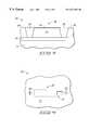
- FIG. 1is a top plan view of a semiconductor wafer fragment in process in accordance with one embodiment of the invention.
- FIG. 2is a diagrammatic side sectional view of the FIG. 1 wafer fragment taken along line 2 — 2 in FIG. 1 .
- FIG. 3is a view of the FIG. 2 wafer fragment at a processing step subsequent to that shown in FIG. 2 .
- FIG. 4is a top plan view of the FIG. 1 wafer fragment at a processing step subsequent to that shown in FIG. 1 .
- FIG. 5is a view which is taken along line 5 — 5 in FIG. 4 .
- FIG. 6is a view of the FIG. 5 wafer fragment at a processing step subsequent to that shown in FIG. 5 .
- FIG. 7is a top plan view of the FIG. 4 wafer fragment at a processing step subsequent to that shown in FIG. 4 .
- FIG. 8is a view of the FIG. 7 wafer fragment taken along line 8 — 8 in FIG. 7 .
- FIG. 9is a view of the FIG. 7 wafer fragment at a processing step subsequent to that shown in FIG. 7 .
- FIG. 10is a view of the FIG. 9 wafer fragment taken along line 10 — 10 in FIG. 9 .
- FIG. 11is a view of the FIG. 9 wafer fragment at a processing step which is subsequent to that shown in FIG. 9 .
- FIG. 12is a view which is taken along line 12 — 12 in FIG. 11 .
- FIG. 13is a view of the FIG. 11 wafer fragment at a processing step subsequent to that shown in FIG. 11 .
- FIG. 14is a view of the FIG. 13 wafer fragment at a processing step subsequent to that shown in FIG. 13 .
- FIG. 15is a view which is taken along line 15 — 15 in FIG. 14 .
- FIG. 16is a view of the FIG. 14 wafer fragment at a processing step subsequent to that shown in FIG. 14 .
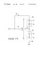
- FIG. 17is a schematic diagram of field effect transistor circuitry constructed in accordance with a preferred embodiment of the invention.
- a semiconductor wafer fragment 20includes a semiconductive substrate 22 having a substrate region 23 .
- Region 23comprises a body of a field effect transistor which is to be formed.
- substrate 22includes a buried mega eV (MeV) layer 24 and a pair of isolation regions 26 which collectively isolate the body.
- substrate region 23comprises p-type material and layer 24 comprises n-type material.
- substrate region 23comprises n-type material and layer 24 comprises p-type material.
- Layer 24 and isolation regions 26define an area 28 over or within which field effect transistor circuitry is to be formed.
- the substratecan comprise any suitable substrate.
- the term “semiconductive substrate”is defined to mean any construction comprising semiconductive material, including, but not limited to, bulk semiconductive materials such as a semiconductive wafer (either alone or in assemblies comprising other materials thereon), and semiconductive material layers (either alone or in assemblies comprising other materials).
- substraterefers to any supporting structure, including, but not limited to, the semiconductive substrates described above.
- the substratecan also comprise silicon-on-insulator substrates formed through various known techniques.
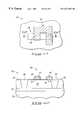
- a gate oxide layer 30is formed over substrate 22 .
- a first patterned masking layer 32is formed over substrate 22 and defines an opening 34 over area 28 .
- Layer 32can comprise photoresist.
- Dopantis introduced into the substrate through opening 34 to form a buried contact diffusion region 36 .
- layer 24comprises an n-type material
- substrate region 23comprises a p-type material
- buried contact diffusion region 36comprises a p+ diffusion region.
- a wet oxide etchcan be conducted either prior to or subsequent to formation of diffusion region 36 to remove portions of oxide layer 30 from over the substrate area where dopant is to be introduced.
- first patterned masking layer 32is removed.
- a conductive material layer 38is formed over substrate 22 and in electrical communication with buried contact diffusion region 36 .
- layer 38is in physical contact with diffusion region 36 .
- An exemplary materialis in situ n-type doped polysilicon.
- a patterned masking layer 40is formed over substrate 22 and defines a conductive line pattern.
- Layer 40can comprise photoresist.
- Conductive layer 38is etched to provide a conductive line 42 which is in electrical communication with buried contact diffusion region 36 (FIG. 12 ).
- Conductive line 42includes a portion 44 which provides a gate for a field effect transistor which is to be formed.
- a patterned masking layer 46is formed over substrate 22 and includes masking openings 48 , 50 and 52 over selected portions of conductive line 42 .
- Exposed conductive line portionsare first doped with a first-type dopant which, in the preferred embodiment, comprises p-type dopant.
- CMOS circuitrycan be contemporaneously formed with the present field effect transistor.
- the p-type doping of the conductive line portionscan also dope other portions of the wafer where, for example, p-channel devices are being formed.
- the p-type regions formed within conductive line 42are spaced-apart along and within the line. Layer 46 is subsequently removed.
- the material comprising conductive line 42is in situ n-type doped polysilicon. Accordingly, the doping of the selected portions of conductive line 42 just described provides alternating regions of p-type dopant and n-type dopant within conductive line 42 . Accordingly, a plurality of pn junctions 66 (FIG. 16) are distributed throughout conductive line 42 . In the event that the material comprising conductive line 42 is not in situ doped n-type polysilicon, or in the event conductive line 42 is desired to be rendered even more n-type, it can be further doped with n-type impurity described just below.
- a patterned masking layer 54is formed over substrate 22 and has masking openings over the illustrated cross-hatched portions of conductive line 42 and other transistor structures which define substrate areas within which source/drain regions are to be formed.
- Exposed conductive line portionsare second doped with a second-type dopant which is different from the first-type dopant.
- the second-type dopantis n-type dopant.
- Dopingalso occurs sufficiently to form source drain regions 62 , 64 (FIG. 15) within substrate 22 . Desired spacing between diffusion regions 64 and 36 , and the dopant concentration of region 23 therebetween, can combine to avoid Zener diode action.
- the doping of the selected portions of conductive line 42 just describedprovides alternating regions of p-type dopant and n-type dopant within conductive line 42 . Accordingly, the dopings define a plurality of pn junctions 66 (FIG. 16) which are distributed throughout conductive line 42 .
- That portion of conductive line 42 comprising the gate line of the transistorcan subjected to silicide processing.
- spacerscan be provided over the line, and a protective layer such as an oxide formed through decomposition of TEOS can be formed over the substrate and subsequently patterned to overlie regions 72 - 80 .
- the protective layercan also overlie other portions of the substrate which are not to be subjected to silicide processing.
- a refractory metalsuch as titanium can be formed over the subject polysilicon, and subsequently heat processed to form a silicide layer over the substrate.
- the silicidecan also be formed over the source/drain regions depending upon design considerations.
- two nodes 68 , 70are provided.
- the nodesare provided by forming openings (designated at “x”) through an insulative material (not shown), and subsequently filling the openings with conductive material.
- Metal linesare provided over the insulative material and comprise node portions which are designated with the lead lines of designators 68 , 70 respectively.
- Node 68provides a reference voltage node which extends to a reference voltage.
- Node 70provides a gate voltage node.
- a plurality of regions 72 , 74 , 76 , 78 and 80are formed within conductive line 42 and are arranged to provide a voltage divider circuit which is connected between gate 44 , body 23 , and reference voltage node 68 .
- the voltage divider circuitis preferably configured to selectively change threshold voltages of the field effect transistor with state changes in the gate voltage as will become apparent below.
- regions 72 - 80are arranged to provide first and second resistive elements received by, supported by, or preferably positioned over the substrate and suitably connected to provide the voltage divider circuit.
- a first resistive elementincludes regions 72 , 74 and 76 (a first p-n-p structure)
- a second resistive elementincludes regions 76 , 78 and 80 (a second p-n-p structure).
- the plurality of regions 72 - 80are arranged within conductive line 42 to provide first and second diode assemblies 82 , 84 (FIG. 17 ).
- the diode assembliesare received by, supported by, or preferably positioned over the substrate, with the first diode assembly 82 connected between gate 44 and body 23 , and second diode assembly 84 connected between body 23 and reference voltage node 68 .
- first diode assembly 82comprises a pair of diodes D 1 , D 2 .
- Each diodehas an anode and a cathode, with the cathodes being connected together in a cathode-connected configuration as shown.
- the anode of diode D 1is connected with gate 44 while the anode of diode D 2 is connected with body 23 .
- Diode assembly 84preferably comprises a pair of diodes D 3 , D 4 , each diode having an anode and a cathode with the cathodes being connected together in a cathode-connected configuration as shown.
- the anode of diode D 3is connected to body 23
- the anode of D 4is connected to reference voltage node 68 .
- the field effect transistor of the present inventionprovides monolithic transistor construction with a bi-level threshold voltage which increases the ratio of I on to I off .
- the transistor's gateis operably connected with the substrate and is configured to change the potential of the substrate. Accordingly, the transistor is selectively configurable by the substrate potential to have different threshold voltages.
- the gate voltage V Gis high (e.g. 3.3 volts)
- the bulk or bodyis at 0 volts and the threshold voltage is adjusted by the enhancement implant to be between 0.5 volts to 0 volts. This is desirable for an aggressive I DS conduction.
- the gate voltage V Gis low (e.g.
- the bulk or bodyis at ⁇ 1.5 volts and the threshold voltage moves up to 1.0 volts according to the doping profile in the bulk of the n-channel device.
- the reference voltage V refis ⁇ 3.0 volts.
- the gate voltagecan be less than 0 volts depending on the gate-induced drain leakage of the device as well.
- Field-effect transistors constructed in accordance with the inventioncan have enhanced speed performance which justifies any increase in circuit layout.
- Other advantages of the inventioncan include a fairly simplified process flow which enhances the manufacturability of the device.
- the field effect transistorcan have improved drive, as well as an improved on/off current ratio. Accordingly, faster devices can be implemented in current CMOS technologies without sacrificing sub 24 threshold and/or stand-by current.
- inventive methods and structureshave been described in the context of n-channel devices, it is to be understood that the inventive methods and structures can be equally well-suited for application with p-channel devices, with consideration being given for the inherent differences between n- and p-channel devices.
Landscapes
- Metal-Oxide And Bipolar Metal-Oxide Semiconductor Integrated Circuits (AREA)
- Semiconductor Integrated Circuits (AREA)
Abstract
Description
Claims (9)
Priority Applications (6)
| Application Number | Priority Date | Filing Date | Title |
|---|---|---|---|
| US09/032,267US6271067B1 (en) | 1998-02-27 | 1998-02-27 | Methods of forming field effect transistors and field effect transistor circuitry |
| US09/266,710US6121665A (en) | 1998-02-27 | 1999-03-11 | Methods of forming field effect transistors and field effect transistor circuitry |
| US09/266,701US6734502B2 (en) | 1998-02-27 | 1999-03-11 | Field effect transistor circuitry |
| US09/545,976US6307238B1 (en) | 1998-02-27 | 2000-04-10 | Methods of forming field effect transistors and field effect transistor circuitry |
| US09/844,819US6746907B2 (en) | 1998-02-27 | 2001-04-27 | Methods of forming field effect transistors and field effect transistor circuitry |
| US09/956,171US6958519B2 (en) | 1998-02-27 | 2001-09-18 | Methods of forming field effect transistors and field effect transistor circuitry |
Applications Claiming Priority (1)
| Application Number | Priority Date | Filing Date | Title |
|---|---|---|---|
| US09/032,267US6271067B1 (en) | 1998-02-27 | 1998-02-27 | Methods of forming field effect transistors and field effect transistor circuitry |
Related Child Applications (3)
| Application Number | Title | Priority Date | Filing Date |
|---|---|---|---|
| US09/266,710DivisionUS6121665A (en) | 1998-02-27 | 1999-03-11 | Methods of forming field effect transistors and field effect transistor circuitry |
| US09/266,701DivisionUS6734502B2 (en) | 1998-02-27 | 1999-03-11 | Field effect transistor circuitry |
| US09/844,819ContinuationUS6746907B2 (en) | 1998-02-27 | 2001-04-27 | Methods of forming field effect transistors and field effect transistor circuitry |
Publications (1)
| Publication Number | Publication Date |
|---|---|
| US6271067B1true US6271067B1 (en) | 2001-08-07 |
Family
ID=21864011
Family Applications (6)
| Application Number | Title | Priority Date | Filing Date |
|---|---|---|---|
| US09/032,267Expired - LifetimeUS6271067B1 (en) | 1998-02-27 | 1998-02-27 | Methods of forming field effect transistors and field effect transistor circuitry |
| US09/266,701Expired - Fee RelatedUS6734502B2 (en) | 1998-02-27 | 1999-03-11 | Field effect transistor circuitry |
| US09/266,710Expired - LifetimeUS6121665A (en) | 1998-02-27 | 1999-03-11 | Methods of forming field effect transistors and field effect transistor circuitry |
| US09/545,976Expired - LifetimeUS6307238B1 (en) | 1998-02-27 | 2000-04-10 | Methods of forming field effect transistors and field effect transistor circuitry |
| US09/844,819Expired - Fee RelatedUS6746907B2 (en) | 1998-02-27 | 2001-04-27 | Methods of forming field effect transistors and field effect transistor circuitry |
| US09/956,171Expired - LifetimeUS6958519B2 (en) | 1998-02-27 | 2001-09-18 | Methods of forming field effect transistors and field effect transistor circuitry |
Family Applications After (5)
| Application Number | Title | Priority Date | Filing Date |
|---|---|---|---|
| US09/266,701Expired - Fee RelatedUS6734502B2 (en) | 1998-02-27 | 1999-03-11 | Field effect transistor circuitry |
| US09/266,710Expired - LifetimeUS6121665A (en) | 1998-02-27 | 1999-03-11 | Methods of forming field effect transistors and field effect transistor circuitry |
| US09/545,976Expired - LifetimeUS6307238B1 (en) | 1998-02-27 | 2000-04-10 | Methods of forming field effect transistors and field effect transistor circuitry |
| US09/844,819Expired - Fee RelatedUS6746907B2 (en) | 1998-02-27 | 2001-04-27 | Methods of forming field effect transistors and field effect transistor circuitry |
| US09/956,171Expired - LifetimeUS6958519B2 (en) | 1998-02-27 | 2001-09-18 | Methods of forming field effect transistors and field effect transistor circuitry |
Country Status (1)
| Country | Link |
|---|---|
| US (6) | US6271067B1 (en) |
Cited By (4)
| Publication number | Priority date | Publication date | Assignee | Title |
|---|---|---|---|---|
| US6746907B2 (en)* | 1998-02-27 | 2004-06-08 | Micron Technology, Inc. | Methods of forming field effect transistors and field effect transistor circuitry |
| US6798013B2 (en) | 2002-08-28 | 2004-09-28 | Fernando Gonzalez | Vertically integrated flash memory cell and method of fabricating a vertically integrated flash memory cell |
| US20080062088A1 (en)* | 2006-09-13 | 2008-03-13 | Tpo Displays Corp. | Pixel driving circuit and OLED display apparatus and electrionic device using the same |
| US20150170905A1 (en)* | 2007-07-30 | 2015-06-18 | Micron Technology, Inc. | Methods for device fabrication using pitch reduction and related devices |
Families Citing this family (25)
| Publication number | Priority date | Publication date | Assignee | Title |
|---|---|---|---|---|
| US6329691B1 (en)* | 1999-12-13 | 2001-12-11 | Tower Semiconductor Ltd. | Device for protection of sensitive gate dielectrics of advanced non-volatile memory devices from damage due to plasma charging |
| US6818930B2 (en)* | 2002-11-12 | 2004-11-16 | Micron Technology, Inc. | Gated isolation structure for imagers |
| US7087978B1 (en)* | 2003-08-01 | 2006-08-08 | National Semiconductor Corporation | Semiconductor resistor with improved width accuracy |
| KR100585886B1 (en)* | 2004-01-27 | 2006-06-01 | 삼성전자주식회사 | Semiconductor circuit with dynamic threshold voltage |
| US8247840B2 (en)* | 2004-07-07 | 2012-08-21 | Semi Solutions, Llc | Apparatus and method for improved leakage current of silicon on insulator transistors using a forward biased diode |
| US7224205B2 (en)* | 2004-07-07 | 2007-05-29 | Semi Solutions, Llc | Apparatus and method for improving drive-strength and leakage of deep submicron MOS transistors |
| US7683433B2 (en)* | 2004-07-07 | 2010-03-23 | Semi Solution, Llc | Apparatus and method for improving drive-strength and leakage of deep submicron MOS transistors |
| US7375402B2 (en)* | 2004-07-07 | 2008-05-20 | Semi Solutions, Llc | Method and apparatus for increasing stability of MOS memory cells |
| US7651905B2 (en)* | 2005-01-12 | 2010-01-26 | Semi Solutions, Llc | Apparatus and method for reducing gate leakage in deep sub-micron MOS transistors using semi-rectifying contacts |
| EP1831932B1 (en)* | 2004-12-29 | 2013-05-08 | Semi Solutions LLC. | Apparatus and method for improving drive strength, leakage and stability of deep submicron mos transistors and memory cells |
| US7898297B2 (en)* | 2005-01-04 | 2011-03-01 | Semi Solution, Llc | Method and apparatus for dynamic threshold voltage control of MOS transistors in dynamic logic circuits |
| US7286417B2 (en)* | 2005-06-21 | 2007-10-23 | Micron Technology, Inc. | Low power dissipation voltage generator |
| US7863689B2 (en)* | 2006-09-19 | 2011-01-04 | Semi Solutions, Llc. | Apparatus for using a well current source to effect a dynamic threshold voltage of a MOS transistor |
| US7864492B2 (en)* | 2006-10-31 | 2011-01-04 | Siemens Industry, Inc. | Systems and methods for arc fault detection |
| US8207784B2 (en)* | 2008-02-12 | 2012-06-26 | Semi Solutions, Llc | Method and apparatus for MOSFET drain-source leakage reduction |
| US8004340B2 (en)* | 2009-12-08 | 2011-08-23 | Stmicroelectronics Asia Pacific Pte. Ltd. | System and method for a semiconductor switch |
| WO2012112594A2 (en)* | 2011-02-14 | 2012-08-23 | California Institute Of Technology | Systems and methods for dynamic mosfet body biasing for low power, fast response vlsi applications |
| US8829967B2 (en) | 2012-06-27 | 2014-09-09 | Triquint Semiconductor, Inc. | Body-contacted partially depleted silicon on insulator transistor |
| US8729952B2 (en) | 2012-08-16 | 2014-05-20 | Triquint Semiconductor, Inc. | Switching device with non-negative biasing |
| US8847672B2 (en)* | 2013-01-15 | 2014-09-30 | Triquint Semiconductor, Inc. | Switching device with resistive divider |
| US9214932B2 (en) | 2013-02-11 | 2015-12-15 | Triquint Semiconductor, Inc. | Body-biased switching device |
| US8923782B1 (en) | 2013-02-20 | 2014-12-30 | Triquint Semiconductor, Inc. | Switching device with diode-biased field-effect transistor (FET) |
| US8977217B1 (en) | 2013-02-20 | 2015-03-10 | Triquint Semiconductor, Inc. | Switching device with negative bias circuit |
| US9203396B1 (en) | 2013-02-22 | 2015-12-01 | Triquint Semiconductor, Inc. | Radio frequency switch device with source-follower |
| US9379698B2 (en) | 2014-02-04 | 2016-06-28 | Triquint Semiconductor, Inc. | Field effect transistor switching circuit |
Citations (14)
| Publication number | Priority date | Publication date | Assignee | Title |
|---|---|---|---|---|
| US3577019A (en)* | 1968-09-24 | 1971-05-04 | Gen Electric | Insulated gate field effect transistor used as a voltage-controlled linear resistor |
| US4246502A (en)* | 1978-08-16 | 1981-01-20 | Mitel Corporation | Means for coupling incompatible signals to an integrated circuit and for deriving operating supply therefrom |
| US4297721A (en)* | 1978-11-03 | 1981-10-27 | Mostek Corporation | Extremely low current load device for integrated circuit |
| US5250457A (en) | 1992-02-19 | 1993-10-05 | Micron Technology, Inc. | Method of forming a buried bit line array of memory cells |
| US5268323A (en)* | 1991-06-26 | 1993-12-07 | Eurosil Electronic Gmbh | Semiconductor array and method for its manufacture |
| US5317282A (en)* | 1991-10-16 | 1994-05-31 | Temic Telefunken Microelectronic Gmbh | Tetrode biasing circuit |
| US5629536A (en) | 1995-11-21 | 1997-05-13 | Motorola, Inc. | High voltage current limiter and method for making |
| US5631187A (en)* | 1988-12-02 | 1997-05-20 | Motorola, Inc. | Method for making semiconductor device having high energy sustaining capability and a temperature compensated sustaining voltage |
| US5681778A (en)* | 1995-11-27 | 1997-10-28 | Micron Technology, Inc. | Semiconductor processing method of forming a buried contact and conductive line |
| US5734175A (en) | 1994-11-14 | 1998-03-31 | Rohm Co., Ltd. | Insulated-gate semiconductor device having a position recognizing pattern directly on the gate contact area |
| US5744842A (en) | 1996-08-15 | 1998-04-28 | Industrial Technology Research Institute | Area-efficient VDD-to-VSS ESD protection circuit |
| US5847597A (en) | 1994-02-28 | 1998-12-08 | Mitsubishi Denki Kabushiki Kaisha | Potential detecting circuit for determining whether a detected potential has reached a prescribed level, and a semiconductor integrated circuit including the same |
| US6107664A (en) | 1996-07-16 | 2000-08-22 | Sgs-Thomson Microelectronics S.A. | Self-locking static micro-circuit breaker |
| US6121665A (en) | 1998-02-27 | 2000-09-19 | Micron Technology, Inc. | Methods of forming field effect transistors and field effect transistor circuitry |
Family Cites Families (21)
| Publication number | Priority date | Publication date | Assignee | Title |
|---|---|---|---|---|
| US4112481A (en)* | 1977-05-05 | 1978-09-05 | Wescom, Inc. | Miniature multi-impedance transformer module |
| SE435436B (en) | 1983-02-16 | 1984-09-24 | Asea Ab | DOUBLE FLOOD PROTECTION |
| US5093646A (en)* | 1988-04-29 | 1992-03-03 | Fmtt, Inc. | High frequency matrix transformer |
| US5389469A (en)* | 1993-06-14 | 1995-02-14 | Rayovac Corporation | AgO battery, and material |
| JPH0729752A (en)* | 1993-07-09 | 1995-01-31 | Mitsubishi Electric Corp | Ignition coil for internal combustion engine |
| KR950021600A (en) | 1993-12-09 | 1995-07-26 | 가나이 쯔또무 | Semiconductor integrated circuit device and manufacturing method thereof |
| JPH10270734A (en)* | 1997-03-27 | 1998-10-09 | Canon Inc | Solar cell module |
| JPH11150287A (en)* | 1997-09-10 | 1999-06-02 | Canon Inc | Solar cell module, enclosure with solar cell, method of installing enclosure with solar cell, and solar power generation system |
| JP3792867B2 (en)* | 1997-11-06 | 2006-07-05 | キヤノン株式会社 | Solar cell module, solar cell array, and solar power generation apparatus construction method |
| US6114197A (en)* | 1998-02-26 | 2000-09-05 | Sharp Laboratories Of America, Inc. | Method of forming fully depleted SIMOX CMOS having electrostatic discharge protection |
| JP3937654B2 (en)* | 1998-06-30 | 2007-06-27 | キヤノン株式会社 | SOLAR CELL MODULE, ITS INSTALLATION METHOD, AND SOLAR POWER GENERATOR AND ROOF USING THE SAME |
| JP2001345472A (en)* | 2000-03-29 | 2001-12-14 | Canon Inc | Inspection method for solar cell module, inspection apparatus and manufacturing method, inspection method and inspection apparatus for photovoltaic power generation system, insulation resistance measuring instrument and withstand voltage tester |
| JP2002111038A (en)* | 2000-09-29 | 2002-04-12 | Canon Inc | Solar cell module, method of manufacturing the same, and power generation device |
| JP2003052185A (en)* | 2001-05-30 | 2003-02-21 | Canon Inc | Power converter, photovoltaic element module using the same, and power generator |
| TW569013B (en)* | 2002-02-21 | 2004-01-01 | Via Tech Inc | Chip test method for testing host controller of universal serial bus |
| JP2003333861A (en)* | 2002-05-10 | 2003-11-21 | Canon Inc | Power supply device, design method thereof, and power generation device |
| JP2004207700A (en)* | 2002-12-11 | 2004-07-22 | Canon Inc | Electronic component and method of manufacturing the same |
| AU2003270988A1 (en)* | 2002-12-19 | 2004-07-08 | Canon Kabushiki Kaisha | Electrical Device, Transformer, and Inductor, and Method of Manufacturing Electrical Device |
| JP2004335886A (en)* | 2003-05-09 | 2004-11-25 | Canon Inc | Transformer assembly, power conversion device and solar power generation device using the same |
| JP2004336944A (en)* | 2003-05-09 | 2004-11-25 | Canon Inc | Power conversion device and solar power generation system |
| US20040246087A1 (en)* | 2003-05-09 | 2004-12-09 | Canon Kabushiki Kaisha | Electric component and method of producing the same |
- 1998
- 1998-02-27USUS09/032,267patent/US6271067B1/ennot_activeExpired - Lifetime
- 1999
- 1999-03-11USUS09/266,701patent/US6734502B2/ennot_activeExpired - Fee Related
- 1999-03-11USUS09/266,710patent/US6121665A/ennot_activeExpired - Lifetime
- 2000
- 2000-04-10USUS09/545,976patent/US6307238B1/ennot_activeExpired - Lifetime
- 2001
- 2001-04-27USUS09/844,819patent/US6746907B2/ennot_activeExpired - Fee Related
- 2001-09-18USUS09/956,171patent/US6958519B2/ennot_activeExpired - Lifetime
Patent Citations (14)
| Publication number | Priority date | Publication date | Assignee | Title |
|---|---|---|---|---|
| US3577019A (en)* | 1968-09-24 | 1971-05-04 | Gen Electric | Insulated gate field effect transistor used as a voltage-controlled linear resistor |
| US4246502A (en)* | 1978-08-16 | 1981-01-20 | Mitel Corporation | Means for coupling incompatible signals to an integrated circuit and for deriving operating supply therefrom |
| US4297721A (en)* | 1978-11-03 | 1981-10-27 | Mostek Corporation | Extremely low current load device for integrated circuit |
| US5631187A (en)* | 1988-12-02 | 1997-05-20 | Motorola, Inc. | Method for making semiconductor device having high energy sustaining capability and a temperature compensated sustaining voltage |
| US5268323A (en)* | 1991-06-26 | 1993-12-07 | Eurosil Electronic Gmbh | Semiconductor array and method for its manufacture |
| US5317282A (en)* | 1991-10-16 | 1994-05-31 | Temic Telefunken Microelectronic Gmbh | Tetrode biasing circuit |
| US5250457A (en) | 1992-02-19 | 1993-10-05 | Micron Technology, Inc. | Method of forming a buried bit line array of memory cells |
| US5847597A (en) | 1994-02-28 | 1998-12-08 | Mitsubishi Denki Kabushiki Kaisha | Potential detecting circuit for determining whether a detected potential has reached a prescribed level, and a semiconductor integrated circuit including the same |
| US5734175A (en) | 1994-11-14 | 1998-03-31 | Rohm Co., Ltd. | Insulated-gate semiconductor device having a position recognizing pattern directly on the gate contact area |
| US5629536A (en) | 1995-11-21 | 1997-05-13 | Motorola, Inc. | High voltage current limiter and method for making |
| US5681778A (en)* | 1995-11-27 | 1997-10-28 | Micron Technology, Inc. | Semiconductor processing method of forming a buried contact and conductive line |
| US6107664A (en) | 1996-07-16 | 2000-08-22 | Sgs-Thomson Microelectronics S.A. | Self-locking static micro-circuit breaker |
| US5744842A (en) | 1996-08-15 | 1998-04-28 | Industrial Technology Research Institute | Area-efficient VDD-to-VSS ESD protection circuit |
| US6121665A (en) | 1998-02-27 | 2000-09-19 | Micron Technology, Inc. | Methods of forming field effect transistors and field effect transistor circuitry |
Non-Patent Citations (2)
| Title |
|---|
| Physics of Semiconductor Devices, by Simon M. Sze, Wiley-Interscience 1969, pp. 505-512. |
| Solid State Electronic Devices, by Benjamin G.Streetman, Prentice-Hall 1972, pp. 293-300. |
Cited By (9)
| Publication number | Priority date | Publication date | Assignee | Title |
|---|---|---|---|---|
| US6746907B2 (en)* | 1998-02-27 | 2004-06-08 | Micron Technology, Inc. | Methods of forming field effect transistors and field effect transistor circuitry |
| US6798013B2 (en) | 2002-08-28 | 2004-09-28 | Fernando Gonzalez | Vertically integrated flash memory cell and method of fabricating a vertically integrated flash memory cell |
| US20050139950A1 (en)* | 2002-08-28 | 2005-06-30 | Fernando Gonzalez | Vertically integrated flash memory cell and method of fabricating a vertically integrated flash memory cell |
| US7098122B2 (en) | 2002-08-28 | 2006-08-29 | Micron Technology, Inc. | Method of fabricating a vertically integrated memory cell |
| US20080062088A1 (en)* | 2006-09-13 | 2008-03-13 | Tpo Displays Corp. | Pixel driving circuit and OLED display apparatus and electrionic device using the same |
| US20150170905A1 (en)* | 2007-07-30 | 2015-06-18 | Micron Technology, Inc. | Methods for device fabrication using pitch reduction and related devices |
| US10522348B2 (en) | 2007-07-30 | 2019-12-31 | Micron Technology, Inc. | Methods for device fabrication using pitch reduction |
| US11348788B2 (en) | 2007-07-30 | 2022-05-31 | Micron Technology, Inc. | Methods for device fabrication using pitch reduction |
| US12400857B2 (en) | 2007-07-30 | 2025-08-26 | Micron Technology, Inc. | Methods of forming electronic devices using pitch reduction |
Also Published As
| Publication number | Publication date |
|---|---|
| US20020017678A1 (en) | 2002-02-14 |
| US6746907B2 (en) | 2004-06-08 |
| US20020096720A1 (en) | 2002-07-25 |
| US20010016378A1 (en) | 2001-08-23 |
| US6307238B1 (en) | 2001-10-23 |
| US6734502B2 (en) | 2004-05-11 |
| US6958519B2 (en) | 2005-10-25 |
| US6121665A (en) | 2000-09-19 |
Similar Documents
| Publication | Publication Date | Title |
|---|---|---|
| US6271067B1 (en) | Methods of forming field effect transistors and field effect transistor circuitry | |
| JP4664631B2 (en) | Semiconductor device and manufacturing method thereof | |
| EP0749165B1 (en) | Thin film transistor in insulated semiconductor substrate and manufacturing method thereof | |
| US7208386B2 (en) | Drain extended MOS transistor with improved breakdown robustness | |
| US6531356B1 (en) | Semiconductor devices and methods of manufacturing the same | |
| US6507080B2 (en) | MOS transistor and fabrication method thereof | |
| US7122861B2 (en) | Semiconductor device and manufacturing method thereof | |
| WO2002052649A1 (en) | Semiconductor device and portable electronic device | |
| US8227862B2 (en) | Semiconductor device | |
| JP2870635B2 (en) | Semiconductor device | |
| US9219117B2 (en) | Semiconductor structure and a method for processing a carrier | |
| EP0524030B1 (en) | Semiconductor device equipped with a high-voltage misfet | |
| JP3282375B2 (en) | Complementary insulated gate field effect transistor | |
| US6348382B1 (en) | Integration process to increase high voltage breakdown performance | |
| EP0989613A1 (en) | SOI transistor with body contact and method of forming same | |
| JP2903892B2 (en) | Method for manufacturing field effect transistor | |
| US6180983B1 (en) | High-voltage MOS transistor on a silicon on insulator wafer | |
| KR100331844B1 (en) | Complementary metal oxide semiconductor device | |
| JPH1174530A (en) | Semiconductor integrated circuit device and method of manufacturing the same | |
| US6552396B1 (en) | Matched transistors and methods for forming the same | |
| JPH04280474A (en) | Soi structure mosfet | |
| JP2917301B2 (en) | Semiconductor device and manufacturing method thereof | |
| JP2917931B2 (en) | Inverter structure | |
| JP2540754B2 (en) | High voltage transistor | |
| JPH1027901A (en) | Manufacture of mos transistor |
Legal Events
| Date | Code | Title | Description |
|---|---|---|---|
| AS | Assignment | Owner name:MICRON TECHNOLOGY, INC., IDAHO Free format text:ASSIGNMENT OF ASSIGNORS INTEREST;ASSIGNORS:GONZALEZ, FERNANDO;MOULI, CHANDRA;REEL/FRAME:009318/0980 Effective date:19980625 | |
| AS | Assignment | Owner name:MICRON TECHNOLOGY, INC., IDAHO Free format text:RE-RECORD TO REPLACE ASSIGNMENT DOCUMENT, FILED 02-13-1998, WITH A REVISED ASSIGNMENT THAT IDENTIFIES THE SERIAL THE SERIAL NUMBER;ASSIGNORS:GONZALEZ, FERNANDO;MOULI, CHANDRA;REEL/FRAME:009819/0920 Effective date:19990304 | |
| STCF | Information on status: patent grant | Free format text:PATENTED CASE | |
| FEPP | Fee payment procedure | Free format text:PAYOR NUMBER ASSIGNED (ORIGINAL EVENT CODE: ASPN); ENTITY STATUS OF PATENT OWNER: LARGE ENTITY | |
| CC | Certificate of correction | ||
| FPAY | Fee payment | Year of fee payment:4 | |
| FPAY | Fee payment | Year of fee payment:8 | |
| FPAY | Fee payment | Year of fee payment:12 | |
| AS | Assignment | Owner name:U.S. BANK NATIONAL ASSOCIATION, AS COLLATERAL AGENT, CALIFORNIA Free format text:SECURITY INTEREST;ASSIGNOR:MICRON TECHNOLOGY, INC.;REEL/FRAME:038669/0001 Effective date:20160426 Owner name:U.S. BANK NATIONAL ASSOCIATION, AS COLLATERAL AGEN Free format text:SECURITY INTEREST;ASSIGNOR:MICRON TECHNOLOGY, INC.;REEL/FRAME:038669/0001 Effective date:20160426 | |
| AS | Assignment | Owner name:MORGAN STANLEY SENIOR FUNDING, INC., AS COLLATERAL AGENT, MARYLAND Free format text:PATENT SECURITY AGREEMENT;ASSIGNOR:MICRON TECHNOLOGY, INC.;REEL/FRAME:038954/0001 Effective date:20160426 Owner name:MORGAN STANLEY SENIOR FUNDING, INC., AS COLLATERAL Free format text:PATENT SECURITY AGREEMENT;ASSIGNOR:MICRON TECHNOLOGY, INC.;REEL/FRAME:038954/0001 Effective date:20160426 | |
| AS | Assignment | Owner name:U.S. BANK NATIONAL ASSOCIATION, AS COLLATERAL AGENT, CALIFORNIA Free format text:CORRECTIVE ASSIGNMENT TO CORRECT THE REPLACE ERRONEOUSLY FILED PATENT #7358718 WITH THE CORRECT PATENT #7358178 PREVIOUSLY RECORDED ON REEL 038669 FRAME 0001. ASSIGNOR(S) HEREBY CONFIRMS THE SECURITY INTEREST;ASSIGNOR:MICRON TECHNOLOGY, INC.;REEL/FRAME:043079/0001 Effective date:20160426 Owner name:U.S. BANK NATIONAL ASSOCIATION, AS COLLATERAL AGEN Free format text:CORRECTIVE ASSIGNMENT TO CORRECT THE REPLACE ERRONEOUSLY FILED PATENT #7358718 WITH THE CORRECT PATENT #7358178 PREVIOUSLY RECORDED ON REEL 038669 FRAME 0001. ASSIGNOR(S) HEREBY CONFIRMS THE SECURITY INTEREST;ASSIGNOR:MICRON TECHNOLOGY, INC.;REEL/FRAME:043079/0001 Effective date:20160426 | |
| AS | Assignment | Owner name:MICRON TECHNOLOGY, INC., IDAHO Free format text:RELEASE BY SECURED PARTY;ASSIGNOR:U.S. BANK NATIONAL ASSOCIATION, AS COLLATERAL AGENT;REEL/FRAME:047243/0001 Effective date:20180629 | |
| AS | Assignment | Owner name:MICRON TECHNOLOGY, INC., IDAHO Free format text:RELEASE BY SECURED PARTY;ASSIGNOR:MORGAN STANLEY SENIOR FUNDING, INC., AS COLLATERAL AGENT;REEL/FRAME:050937/0001 Effective date:20190731 |