US6271060B1 - Process of fabricating a chip scale surface mount package for semiconductor device - Google Patents
Process of fabricating a chip scale surface mount package for semiconductor deviceDownload PDFInfo
- Publication number
- US6271060B1 US6271060B1US09/395,095US39509599AUS6271060B1US 6271060 B1US6271060 B1US 6271060B1US 39509599 AUS39509599 AUS 39509599AUS 6271060 B1US6271060 B1US 6271060B1
- Authority
- US
- United States
- Prior art keywords
- die
- wafer
- substrate
- dice
- front side
- Prior art date
- Legal status (The legal status is an assumption and is not a legal conclusion. Google has not performed a legal analysis and makes no representation as to the accuracy of the status listed.)
- Expired - Lifetime
Links
Images


Classifications
- H—ELECTRICITY
- H01—ELECTRIC ELEMENTS
- H01L—SEMICONDUCTOR DEVICES NOT COVERED BY CLASS H10
- H01L25/00—Assemblies consisting of a plurality of semiconductor or other solid state devices
- H01L25/50—Multistep manufacturing processes of assemblies consisting of devices, the devices being individual devices of subclass H10D or integrated devices of class H10
- H—ELECTRICITY
- H01—ELECTRIC ELEMENTS
- H01L—SEMICONDUCTOR DEVICES NOT COVERED BY CLASS H10
- H01L21/00—Processes or apparatus adapted for the manufacture or treatment of semiconductor or solid state devices or of parts thereof
- H01L21/02—Manufacture or treatment of semiconductor devices or of parts thereof
- H01L21/04—Manufacture or treatment of semiconductor devices or of parts thereof the devices having potential barriers, e.g. a PN junction, depletion layer or carrier concentration layer
- H01L21/50—Assembly of semiconductor devices using processes or apparatus not provided for in a single one of the groups H01L21/18 - H01L21/326 or H10D48/04 - H10D48/07 e.g. sealing of a cap to a base of a container
- H01L21/60—Attaching or detaching leads or other conductive members, to be used for carrying current to or from the device in operation
- H—ELECTRICITY
- H01—ELECTRIC ELEMENTS
- H01L—SEMICONDUCTOR DEVICES NOT COVERED BY CLASS H10
- H01L23/00—Details of semiconductor or other solid state devices
- H01L23/48—Arrangements for conducting electric current to or from the solid state body in operation, e.g. leads, terminal arrangements ; Selection of materials therefor
- H01L23/488—Arrangements for conducting electric current to or from the solid state body in operation, e.g. leads, terminal arrangements ; Selection of materials therefor consisting of soldered or bonded constructions
- H01L23/498—Leads, i.e. metallisations or lead-frames on insulating substrates, e.g. chip carriers
- H01L23/49805—Leads, i.e. metallisations or lead-frames on insulating substrates, e.g. chip carriers the leads being also applied on the sidewalls or the bottom of the substrate, e.g. leadless packages for surface mounting
- H—ELECTRICITY
- H01—ELECTRIC ELEMENTS
- H01L—SEMICONDUCTOR DEVICES NOT COVERED BY CLASS H10
- H01L25/00—Assemblies consisting of a plurality of semiconductor or other solid state devices
- H01L25/03—Assemblies consisting of a plurality of semiconductor or other solid state devices all the devices being of a type provided for in a single subclass of subclasses H10B, H10D, H10F, H10H, H10K or H10N, e.g. assemblies of rectifier diodes
- H01L25/04—Assemblies consisting of a plurality of semiconductor or other solid state devices all the devices being of a type provided for in a single subclass of subclasses H10B, H10D, H10F, H10H, H10K or H10N, e.g. assemblies of rectifier diodes the devices not having separate containers
- H01L25/065—Assemblies consisting of a plurality of semiconductor or other solid state devices all the devices being of a type provided for in a single subclass of subclasses H10B, H10D, H10F, H10H, H10K or H10N, e.g. assemblies of rectifier diodes the devices not having separate containers the devices being of a type provided for in group H10D89/00
- H01L25/0657—Stacked arrangements of devices
- H—ELECTRICITY
- H01—ELECTRIC ELEMENTS
- H01L—SEMICONDUCTOR DEVICES NOT COVERED BY CLASS H10
- H01L2225/00—Details relating to assemblies covered by the group H01L25/00 but not provided for in its subgroups
- H01L2225/03—All the devices being of a type provided for in the same main group of the same subclass of class H10, e.g. assemblies of rectifier diodes
- H01L2225/04—All the devices being of a type provided for in the same main group of the same subclass of class H10, e.g. assemblies of rectifier diodes the devices not having separate containers
- H01L2225/065—All the devices being of a type provided for in the same main group of the same subclass of class H10
- H01L2225/06503—Stacked arrangements of devices
- H01L2225/06513—Bump or bump-like direct electrical connections between devices, e.g. flip-chip connection, solder bumps
- H—ELECTRICITY
- H01—ELECTRIC ELEMENTS
- H01L—SEMICONDUCTOR DEVICES NOT COVERED BY CLASS H10
- H01L2225/00—Details relating to assemblies covered by the group H01L25/00 but not provided for in its subgroups
- H01L2225/03—All the devices being of a type provided for in the same main group of the same subclass of class H10, e.g. assemblies of rectifier diodes
- H01L2225/04—All the devices being of a type provided for in the same main group of the same subclass of class H10, e.g. assemblies of rectifier diodes the devices not having separate containers
- H01L2225/065—All the devices being of a type provided for in the same main group of the same subclass of class H10
- H01L2225/06503—Stacked arrangements of devices
- H01L2225/06517—Bump or bump-like direct electrical connections from device to substrate
- H—ELECTRICITY
- H01—ELECTRIC ELEMENTS
- H01L—SEMICONDUCTOR DEVICES NOT COVERED BY CLASS H10
- H01L2225/00—Details relating to assemblies covered by the group H01L25/00 but not provided for in its subgroups
- H01L2225/03—All the devices being of a type provided for in the same main group of the same subclass of class H10, e.g. assemblies of rectifier diodes
- H01L2225/04—All the devices being of a type provided for in the same main group of the same subclass of class H10, e.g. assemblies of rectifier diodes the devices not having separate containers
- H01L2225/065—All the devices being of a type provided for in the same main group of the same subclass of class H10
- H01L2225/06503—Stacked arrangements of devices
- H01L2225/06551—Conductive connections on the side of the device
- H—ELECTRICITY
- H01—ELECTRIC ELEMENTS
- H01L—SEMICONDUCTOR DEVICES NOT COVERED BY CLASS H10
- H01L2225/00—Details relating to assemblies covered by the group H01L25/00 but not provided for in its subgroups
- H01L2225/03—All the devices being of a type provided for in the same main group of the same subclass of class H10, e.g. assemblies of rectifier diodes
- H01L2225/04—All the devices being of a type provided for in the same main group of the same subclass of class H10, e.g. assemblies of rectifier diodes the devices not having separate containers
- H01L2225/065—All the devices being of a type provided for in the same main group of the same subclass of class H10
- H01L2225/06503—Stacked arrangements of devices
- H01L2225/06582—Housing for the assembly, e.g. chip scale package [CSP]
- H01L2225/06586—Housing with external bump or bump-like connectors
- H—ELECTRICITY
- H01—ELECTRIC ELEMENTS
- H01L—SEMICONDUCTOR DEVICES NOT COVERED BY CLASS H10
- H01L2924/00—Indexing scheme for arrangements or methods for connecting or disconnecting semiconductor or solid-state bodies as covered by H01L24/00
- H01L2924/0001—Technical content checked by a classifier
- H01L2924/0002—Not covered by any one of groups H01L24/00, H01L24/00 and H01L2224/00
- H—ELECTRICITY
- H01—ELECTRIC ELEMENTS
- H01L—SEMICONDUCTOR DEVICES NOT COVERED BY CLASS H10
- H01L2924/00—Indexing scheme for arrangements or methods for connecting or disconnecting semiconductor or solid-state bodies as covered by H01L24/00
- H01L2924/095—Indexing scheme for arrangements or methods for connecting or disconnecting semiconductor or solid-state bodies as covered by H01L24/00 with a principal constituent of the material being a combination of two or more materials provided in the groups H01L2924/013 - H01L2924/0715
- H01L2924/097—Glass-ceramics, e.g. devitrified glass
- H01L2924/09701—Low temperature co-fired ceramic [LTCC]
- H—ELECTRICITY
- H01—ELECTRIC ELEMENTS
- H01L—SEMICONDUCTOR DEVICES NOT COVERED BY CLASS H10
- H01L2924/00—Indexing scheme for arrangements or methods for connecting or disconnecting semiconductor or solid-state bodies as covered by H01L24/00
- H01L2924/10—Details of semiconductor or other solid state devices to be connected
- H01L2924/11—Device type
- H01L2924/12—Passive devices, e.g. 2 terminal devices
- H01L2924/1204—Optical Diode
- H01L2924/12044—OLED
Definitions
- the resulting integrated circuit (IC) chips or dicemust be separated and packaged in such a way that they can be connected to external circuitry.
- ICintegrated circuit
- packaging techniquesMost involve mounting the die on a leadframe, connecting the die pads to the leadframe by wire-bonding or otherwise, and then encapsulating the die and wire bonds in a plastic capsule, with the leadframe left protruding from the capsule. The encapsulation is often done by injection-molding. The leadframe is then trimmed to remove the tie bars that hold it together, and the leads are bent in such a way that the package can be mounted on a flat surface, typically a printed circuit board (PCB).
- PCBprinted circuit board
- a power MOSFETtypically has its source and gate terminals on the front side of the die and its drain terminal on the back side of the die.
- a vertical diodehas its anode terminal on one face of the die and its cathode terminal on the opposite face of the die.
- Bipolar transistors, junction field effect transistors (JFETs), and various types of integrated circuits (ICs)can also be fabricated in a “vertical” configuration.
- the fabrication processstarts with a semiconductor wafer including a plurality of dice and includes: forming an overcoat on a surface of the wafer; attaching the wafer to a substrate; patterning the overcoat to expose connection pads on a front side of the dice; forming an electrically conductive wraparound layer on a side of a die, the wraparound layer wrapping around an edge of the die to form at least a portion of an electrical connection between a location on the front side of the die and a terminal on a back side of the die; and breaking the wafer into individual dice.
- the formation of a wraparound layerincludes severing the wafer along parallel lines between the dice so as to yield a plurality of multiple-die strips; mounting the strips adjacent to each other, sandwich-like, to form a stack; depositing at least a first metal layer on an exposed side of the stack, the first metal layer wrapping around the edge of each die to form an electrical connection between the front side of the die and an electrical terminal on the back side of the die; disassembling the strips in the stack; separating the individual dice in the strips; and plating a second metal layer over the first metal layer.
- the first and second metal layersare, in effect, sublayers of a single metal “layer”.
- the processmay include forming a solderable metal layer on the connection pads.
- the solderable metal layercan be formed, for example, by removing a native oxide layer from the connection pad (e.g., removing aluminum oxide from an aluminum layer) and depositing a solderable metal such as gold, nickel or silver on the exposed metal by sputtering or plating.
- the processmay also include forming solder or polymer bumps or balls on the connection pads on the front side of the die, thereby enabling the package to be mounted to a PCB using known flip-chip techniques.
- perpendicular saw cutsare made between the dice, the cuts extending partially through the substrate such that the substrate remains intact at its back side.
- the multiple-die stripsare formed by breaking the wafer along a series of parallel cuts. After the first metal layer has been deposited and the stack has been disassembled, the strips are broken into individual dice along the cuts perpendicular to those that were broken to form the strips.
- the substratemay be a sheet of a conductive material such as copper or aluminum and may be attached to at least one terminal on a back side of the die with a conductive cement.
- the conductive substratemay serve as a heat sink as well as an electrical contact.
- the substratemay be nonconductive, and vias or holes may be formed in the substrate and filled with a conductive material to facilitate electrical contact with the back side of the die.
- the first metal layeris a relatively thin layer deposited by sputtering or evaporation and the second metal layer is a relatively thick layer formed by plating. In some embodiments, it may be possible to make the first metal layer thick enough that the second metal layer can be omitted.
- the semiconductor waferthinner, for example by grinding the back side of the wafer, to reduce the resistance of the semiconductor device.
- a supporting substratewhich could be made of a nonconductive material such as glass or a conductive material such as copper. Holes are opened in the supporting substrate to expose the connection pads on the front side of the wafer.
- a semiconductor package in accordance with this inventioncomprises a semiconductor die; a supporting substrate attached to a back side of the die; a nonconductive overcoat overlying a front side of the die, an opening in the overcoat corresponding with a connection pad on the front side of the die, and an electrically conductive wraparound layer (which may include a conductive polymer layer or one or more metal layers or sublayers) extending from the front side of the die, around an edge of the die to the substrate, and thereby establishing an electrical connection between a location on the front side of the die and a terminal on the back side of the die.
- a solder or polymer bump or ballcan be formed on the connection pad.
- the semiconductor packageincludes a vertical power MOSFET, and the supporting substrate comprises a sheet of copper.
- the overcoatis patterned so as to expose source and gate pads on the front side of the die.
- the copper substrateis attached with a conductive cement to a drain terminal on the back side of the die, and the wraparound layer extends around an edge of the die to establish an electrical connection between the front side of the die and the copper substrate.
- the portion of the wraparound layer on the front side of the dieeffectively forms a front side drain pad.
- Solder ballsare formed on the source, gate and drain pads.
- the packagecan be inverted and mounted, flip-chip style, on a PCB.
- the substrateis nonconductive, and vias filled with a conductive material extend through the substrate to allow electrical contact between the wraparound layer and the terminal on the back side of the die.
- Semiconductor packages according to this inventiondo not require an epoxy capsule or bond wires; the one or more substrates attached to the die serve to protect the die and act as heat sinks for the die; the packages are very small (e.g., 50% the size of molded packages) and thin; they provide a very low on-resistance for the semiconductor device, particularly if the wafer is ground thinner; they are economical to produce, since they require no molds or lead frames; and they can be used for a wide variety of semiconductor devices such as diodes, MOSFETs, JFETs, bipolar transistors and various types of integrated circuit chips.
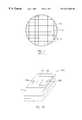
- FIG. 1illustrates a top view of a conventional semiconductor wafer including a plurality of dice.
- FIG. 2Aillustrates a cross-sectional view of a wafer attached to a substrate in accordance with this invention.
- FIG. 2Billustrates a single die of the wafer after the overcoat has been deposited and patterned.
- FIG. 2Cillustrates the wafer after partial cuts have been made along the scribe lines separating the dice.
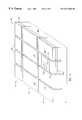
- FIG. 3illustrates a cross-sectional view of strips of dice mounted together to form a stack in accordance with this invention.
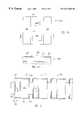
- FIGS. 4A and 4Billustrate top and cross-sectional views, respectively, of one of the dice in the stack.
- FIG. 5illustrates a cross-sectional view of three of the dice in the stack, showing how the metal layers are deposited on the pads and wrap around the edges of the dice to establish an electrical connection with a terminal on the back side of the die.
- FIG. 6illustrates a perspective view of the die after the plating process has been completed.
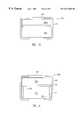
- FIGS. 7A and 7Billustrate top and side views, respectively, of the completed semiconductor package including solder balls for making external connections.
- FIG. 7Cillustrates a side view of a package similar to the one shown in FIGS. 7A and 7B, except that the solder balls have been omitted.
- FIG. 8illustrates a cross-sectional view of an alternative embodiment wherein the supporting substrate is made of a nonconductive material and vias filled with a conductive material are formed in the substrate.
- FIG. 9Ashows an alternative embodiment wherein a supporting substrate is attached to the front side of the wafer to support the wafer as the back side of the wafer is being ground to make the wafer thinner.
- FIG. 9Bshows a cross-sectional view of a semiconductor package fabricated by the process shown in FIG. 9 A.
- FIG. 1illustrates a top view of a wafer 100 and dice 102 .
- the diceare separated by a perpendicular network of scribe lines 104 , where saw cuts are typically made to separate the dice 102 .
- This inventionwill be described with respect to a package for a vertical power MOSFET, which typically has source and gate terminals on its front side and a drain terminal on its back side. It should be understood, however, that the broad principles of this invention can be used to fabricate a package for any type of semiconductor die which has terminals both its front and back sides, including diodes, bipolar transistors, junction field effect transistors (JFETs), and various types of integrated circuits (ICs).
- the “front side” of a dierefers to the side of the die on which the electrical devices and/or a majority of the connection pads are located; “back side” refers to the opposite side of the die.
- a semiconductor dienormally has a top metal layer that includes connection pads used for making interconnections with external devices. Typically, this is an aluminum metal layer, although copper layers are also being used. In most embodiments of this invention, this metal layer needs to be modified so that it will adhere to a solder metal such as tin/lead, for the reasons described below. If there is a native oxide layer on the metal, this native oxide layer must first be removed. Then a solderable metal, such as gold, nickel or silver, is deposited on the exposed metal. The removal of the oxide layer and deposition of a solderable metal can be accomplished by means of a number of known processes.
- an aluminum layercan be sputter-etched to remove the native aluminum oxide layer and then gold, silver or nickel can be sputtered onto the aluminum.
- the diecan be dipped in a liquid etchant to strip away the oxide layer and the solderable metal can then be deposited by electroless or electrolytic plating.
- Electroless platingincludes the use of a “zyering” process to displace the oxide, followed by the plating of nickel to displace the zincate.
- FIG. 2Ashows a rectangular section of a semiconductor wafer 200 containing a number of dice 206 .
- the back side of semiconductor wafer 200is attached to an electrically conductive supporting substrate 202 with a layer of a conductive cement 204 .
- substrate 202is made of copper, but it could also be made of any other conductive material capable of providing support and acting as an electrical contact for wafer 200 .
- Cement 204could be a metallic cement, a silver-filled conductive epoxy or another conductive glue.
- Wafer 200is typically silicon but it could also be another semiconductor material such as silicon carbide or gallium arsenide.
- a metal layer(not shown) is formed on the backside of wafer 200 before the cement 204 is applied to provide good adhesion to the cement.
- the metal layercan include a 500 ⁇ titanium sublayer overlain by a 3,000 ⁇ nickel sublayer and a 1 ⁇ m silver sublayer.
- the titanium, nickel and silver sublayerscan be deposited by evaporation or sputtering.
- Wafer 200includes dice 206 which in this embodiment contain power MOSFETs, but as described above dice 206 could alternatively contain bipolar transistors, diodes, JFETs, ICs or any type of vertical or lateral current-flow device.
- the MOSFETs, bipolar transistors, diodes or other devicesare often formed in a two-dimensional array in each of dice 206 .
- dice 206are separated by a perpendicular network of scribe lines 207 .
- Dice 206have connection pads on their front sides which are exemplified by source pads 208 S and gate pads 208 G shown in one of dice 206 designated die 206 A. There are typically drain pads (not shown) on the backsides of the dice 206 .
- pads 208 S and 208 Gare located in a central region of die 206 A.
- the portion of the front side of die 206 A that is not occupied by pads 208 G and 208 Sis covered by a passivation layer 209 .
- openingsare etched in the passivation layer to expose the gate and source pads.
- an overcoat 210 of polyimide, plastic or glassis formed in the exposed surface of wafer 200 using spin-on, deposition or spray techniques, and overcoat 210 is then patterned using known photolithographic techniques, for example, so as to leave the pads 208 S and 208 G and portions of passivation layer 209 exposed.
- the patterned overcoatcan be formed by other processes such as screen printing.
- screen-printed polyimideis used to form an overcoat that is 1 mil thick.
- FIG. 2Bshows a view of die 206 A after overcoat 210 has been deposited and patterned, leaving pads 208 S and 208 G and portions of passivation layer 209 exposed.
- Overcoat 210can also be formed of a conductive material such as aluminum or copper, but in that case a nonconductive adhesive layer should be formed between the overcoat and the wafer to ensure that the conductive overcoat does not become shorted to the connection pads 208 S and 208 G.
- wafer 200can be screen-printed or laser-marked with markings such as the model number, etc.
- partial cuts 212 X and 212 Yare made in the sandwich of wafer 200 , overcoat 210 and substrate 202 .
- Partial cuts 212 X and 212 Ydo not extend all the way through the sandwich, but they extend entirely through wafer 200 and overcoat 210 and far enough into substrate 202 that substrate 202 can easily be broken at the locations of partial cuts 212 X and 212 Y without damaging the dice 206 .
- partial cuts 212 X and 212 Yare perpendicular to each other and are made at the locations of the scribe lines 207 between the individual dice 206 . Partial cuts 212 X and 212 Y can be made with a conventional dicing saw or, alternatively, by other methods such as laser cutting or photolithographic patterning and etching techniques.
- Wafer 200 and substrate 202are then broken into multichip strips 214 along partial cuts 212 X, each of which contains a row of dice 206 .
- partial cuts 212 Xcan be made somewhat deeper than partial cuts 212 Y.
- partial cuts 212 Xare 5 mils deeper than partial cuts 212 Y.
- a ceramic breaking machinesuch as the Tokyo Weld TWA-100 AG III can be used to break the wafer 200 into strips 214 .
- partial cuts 212 Yare not made at this time, and the strips 214 are separated into individual dice at a later stage in the process.
- partial cuts 212 Yare made before cuts 212 X, and cuts 212 X can extend all the way through the substrate 202 such that there is no need to break the substrate.
- Strips 214are assembled sandwich-like to form a stack 213 , as shown in FIG. 3, which is a cross-sectional view taken at the location of one of the cuts 212 Y.
- strips 214can be held against one another in a magazine or other fixture which contains a cavity shaped to hold the strips 214 in place with one edge of the strips 214 exposed. While only three strips 214 are shown in FIG. 3, as many as 50 or 100 or more strips 214 or can be mounted in the stack.
- FIG. 3also shows the overcoat 210 (exaggerated in thickness) which covers the surface of wafer 200 except where the pads 208 S and 208 G and the exposed portions of passivation layer 209 are located.
- FIG. 4Ashows a top view of die 206 A in one of strips 214 , showing the locations of pads 208 S and 208 G. Also shown are the exposed portions of passivation layer 209 , which are located adjacent an edge of die 206 A.
- FIG. 4Bshows a view taken at cross-section 4 B— 4 B in FIG. 4A, showing how overcoat 210 surrounds the source pad 208 S. It will be evident that overcoat 210 similarly surrounds the gate pad 208 G.
- Strips 214are then exposed to a deposition process by which a first metal layer 215 is sputtered on the exposed portions of passivation layer 209 and on the edges of strips 214 , as shown in the cross-sectional view of FIG. 5 .
- Metal layer 215begins on the front side of the die 206 A and extends around the edge of the die 206 A to conductive substrate 202 , thereby establishing an electrical connection between the front side of die 206 A and the drain terminal of the MOSFET (shown symbolically) within dice 206 .
- metal layer 215contacts both the edge and back side of substrate 202 .
- layer 215can be a layer of nickel or copper 1000 ⁇ thick. Since, as shown in FIGS.
- pads 208 S and 208 Gare totally enclosed by overcoat 210 and the back side of the adjacent strip 214 , the metal does not sputter onto pads 208 S and 208 G.
- another processsuch as evaporation can be used to form metal layer 215 .
- Metal layer 215may extend onto the edges of overcoat 210 but this does not create a problem because the strips 214 will later be separated as described below.
- the stack 213is then turned over in the magazine to expose the opposite edges of the dice 206 , and the same process is performed to create a similar layer 215 on the opposite sides of the dice 206 .
- stack 213is disassembled into individual strips 214 , and the multichip strips 214 are broken into individual dice 206 along the cuts 212 X.
- a Tokyo Weld TWA-100 AG III ceramic breaking machinecan be used to break the strips.
- the individual dice 206are placed in a barrel-plating machine such as one manufactured by HBS or American Plating, and an electroplating process is performed to form a second metal layer 216 over the first metal layer 215 .
- a barrel-plating machinesuch as one manufactured by HBS or American Plating
- an electroplating processis performed to form a second metal layer 216 over the first metal layer 215 .
- other types of electroless plating machines or processescan be used to form second metal layer 216 .
- Metal layer 216forms only on top of the metal layer 215 and does not adhere to overcoat 210 .
- metal layer 216can be a one mil thick layer of a solderable metal such as tin/lead. Metal layer 216 thus creates a good electrical connection between the front side of die 206 A and the copper substrate 202 along opposite edges of the die.
- the overcoat 210is formed of a conductive material, as described above a nonconductive adhesive layer is preferably applied to separate the overcoat from the wafer. This nonconductive layer creates a gap between the overcoat and the connection pads and prevents the plated metal layer from creating a short between the overcoat and the connection pads.
- the second metal layermay be omit by depositing a relatively thick first metal layer by, for example, sputtering or evaporation.
- more than two metal layersmay be deposited to make the connection between the front side of the die and the device terminal on the back side of the die. When two or more layers are deposited, the layers can be viewed, in effect, as sublayers in a single wraparound metal “layer”.
- FIG. 6shows die 206 A after the plating process has been completed, with the front side of die 206 A being connected to substrate 202 by means of the metal layers 215 and 216 .
- the portion of metal layer 216 on the front side of die 206 Abecomes in effect a front side “drain pad.” Since die 206 A contains power MOSFETs, substrate 202 would be in electrical contact with their drain terminals, and thus the front side drain pads would be electrically connected to the drain terminals of the power MOSFETs.
- metal layers 215 and 216would connect the front side of die 206 A to whichever terminals (anodes or cathodes) were located on the back side of the die 206 A. Either pad 208 G or 208 S could be used to connect to the other terminal of the diodes.
- a wraparound conductive polymer or metal layer functionally similar to layers 215 and 216can be formed on die strips 214 using, for example, a machine available from the Nitto company of Japan.
- the electrically conductive wraparound layer connecting the front side of the die and the device terminal on the back side of the diecan be formed after the wafer has been separated into individual dice.
- solder bumps or balls 219can then be formed on the pads 208 S and 208 G and the portions of the metal layer 216 on the front side of die 206 A (the “front side drain pad”), producing the completed package 220 shown in the top view of FIG. 7 A and the side view of FIG. 7 B.
- solder balls 219may be applied in a conventional manner by depositing and reflowing solder paste or by other processes such as screen-printing or solder jetting (using, for example, equipment available from Pac Tech GmbH, Am Sch GmbH, Am Sch GmbH, Am Sch GmbH, Am Sch GmbH, Am Sch GmbH, Am Sch GmbH, Am Sch GmbH, Am Sch GmbH, Am Sch GmbH, Am Sch GmbH, Am Sch GmbH, Am Sch GmbH, Am Sch GmbH, Am Sch GmbH, Am Sch GmbH, 1841 Nauen, Germany) or by using the wafer level solder ball mounter available from Shibuya Kogyo Co., Ltd., Mameda-Honmachi, Kanazawa 920-8681, Japan.
- Conductive polymer bumpsare another alternative, using for example thermosetting polymers, B-state adhesives, or thermoplastic polymers.
- Package 220is then mounted on a PCB or other flat surface by the well-known “flip-chip” technique.
- the solder or polymer bumps or balls 219can be omitted to produce the package 230 shown in the side view of FIG. 7 C.
- FIG. 8shows a package 250 wherein a nonconductive substrate 252 is attached to the back side of die 254 . Vias 256 extend through substrate 252 . Vias 256 are filled with a conductive material 260 that is in electrical contact with a layer 258 of conductive cement. Otherwise, the package is similar to the embodiment described above, with an overcoat 262 deposited on the front side of die 254 and metal layers 264 extending around the edges of die 254 and substrate 252 to make electrical contact with the conductive material 260 .
- Substrate 252could be made of ceramic, aluminum oxide, glass, or plastic.
- Conductive material 260could be a metal.
- Conductive material 260may also extend through the layer 258 so as to make a direct contact with a terminal on the back side of die 254 .
- Vias 256could be formed, for example, by drilling, and they could be filled by a plating process, using machines manufactured by 3M or Nikko Denko.
- Semiconductor wafersare normally on the order of 15 to 30 mils thick. In order to reduce the resistance between the front and back sides of the wafer, it may to desirable to make the wafer thinner. This can be accomplished by processing the back side of the wafer, e.g., by grinding. To provide proper support for the wafer during the grinding process, the front side of the wafer is bonded to a supporting substrate. After the grinding has been completed, the back side of the wafer is attached to a substrate, in the manner in which wafer 200 is attached to a conductive substrate 202 , as shown in FIG. 2A, or a nonconductive substrate 252 , as shown in FIG. 8 . Thus a sandwich is created, including the thinned wafer interposed between the substrates attached to its front and back sides, respectively. Thereafter, the process described above is applied to the sandwich structure.
- FIG. 9Ashows a section of a thinned wafer 300 sandwiched between a front side substrate 302 and a back side substrate 304 .
- Openings 306have been formed in the front side substrate 302 to provide access to connection pads (not shown) and a portion of the passivation layer on the front side of wafer 300 .
- Front side substrate 302could be made of glass or copper and is attached to wafer 300 with a layer 301 of a nonconductive cement such as nonconductive epoxy, for example, to prevent shorting between the connection pads.
- Openings 306could be formed by etching or by a mechanical means such as stamping or drilling, and openings 306 can be performed in front side substrate 302 before substrate 302 is attached to wafer 300 .
- the back side of wafer 300is ground with, for example, a grinding machine available from Strausbaugh after wafer 300 is attached to front side substrate 302 but before wafer 300 is attached to back side substrate 304 .
- Wafer 300may be ground to a thickness of 1-2 mils, for example.
- wafer 300can be thinned by lapping or etching.
- front side substrate 302may eliminate the need for an overcoat on the front side of wafer 300 , or an overcoat may be applied to the front side of wafer 300 before front side substrate 302 is attached.
- FIG. 9AThe sandwich structure shown in FIG. 9A is processed as described above in, for example, FIGS. 2C, 3 , and 5 , to produce a semiconductor package having a wraparound metal layer which establishes an electrical connection between the front side of the die and a device terminal on their back side of the die.
- a cross-sectional view of the resulting package at section 9 B— 9 Bis shown in FIG. 9B, with one or more metal layers 310 wrapping around an edge of die 300 A to form an electrical connection between the front side of die 300 A and a terminal on the back side of die 300 A.
Landscapes
- Engineering & Computer Science (AREA)
- Microelectronics & Electronic Packaging (AREA)
- Power Engineering (AREA)
- Physics & Mathematics (AREA)
- Condensed Matter Physics & Semiconductors (AREA)
- General Physics & Mathematics (AREA)
- Computer Hardware Design (AREA)
- Manufacturing & Machinery (AREA)
- Dicing (AREA)
- Internal Circuitry In Semiconductor Integrated Circuit Devices (AREA)
Abstract
Description
Claims (35)
Priority Applications (8)
| Application Number | Priority Date | Filing Date | Title |
|---|---|---|---|
| US09/395,095US6271060B1 (en) | 1999-09-13 | 1999-09-13 | Process of fabricating a chip scale surface mount package for semiconductor device |
| JP28415199AJP3343535B2 (en) | 1999-09-13 | 1999-10-05 | Semiconductor device package having footprint approximately the same size as semiconductor die and manufacturing process thereof |
| EP99120190AEP1085561B1 (en) | 1999-09-13 | 1999-10-09 | Chip scale surface mount package for semiconductor device and process of fabricating the same |
| SG9905072ASG106568A1 (en) | 1999-09-13 | 1999-10-09 | Chip scale surface mount package for semiconductor device and process of fabricating the same |
| KR10-1999-0045233AKR100419352B1 (en) | 1999-09-13 | 1999-10-19 | Chip scale surface mount package for semiconductor device and process of fabricating the same |
| CNB991243188ACN1177358C (en) | 1999-09-13 | 1999-11-16 | Semiconductor device chip scale surface assembling and packaging, and mfg. method therefor |
| TW088121054ATW441051B (en) | 1999-09-13 | 1999-12-02 | Chip scale surface mount package for semiconductor device and process of fabricating the same |
| US09/733,823US6441475B2 (en) | 1999-09-13 | 2000-12-08 | Chip scale surface mount package for semiconductor device and process of fabricating the same |
Applications Claiming Priority (1)
| Application Number | Priority Date | Filing Date | Title |
|---|---|---|---|
| US09/395,095US6271060B1 (en) | 1999-09-13 | 1999-09-13 | Process of fabricating a chip scale surface mount package for semiconductor device |
Related Child Applications (1)
| Application Number | Title | Priority Date | Filing Date |
|---|---|---|---|
| US09/733,823DivisionUS6441475B2 (en) | 1999-09-13 | 2000-12-08 | Chip scale surface mount package for semiconductor device and process of fabricating the same |
Publications (1)
| Publication Number | Publication Date |
|---|---|
| US6271060B1true US6271060B1 (en) | 2001-08-07 |
Family
ID=23561666
Family Applications (2)
| Application Number | Title | Priority Date | Filing Date |
|---|---|---|---|
| US09/395,095Expired - LifetimeUS6271060B1 (en) | 1999-09-13 | 1999-09-13 | Process of fabricating a chip scale surface mount package for semiconductor device |
| US09/733,823Expired - LifetimeUS6441475B2 (en) | 1999-09-13 | 2000-12-08 | Chip scale surface mount package for semiconductor device and process of fabricating the same |
Family Applications After (1)
| Application Number | Title | Priority Date | Filing Date |
|---|---|---|---|
| US09/733,823Expired - LifetimeUS6441475B2 (en) | 1999-09-13 | 2000-12-08 | Chip scale surface mount package for semiconductor device and process of fabricating the same |
Country Status (7)
| Country | Link |
|---|---|
| US (2) | US6271060B1 (en) |
| EP (1) | EP1085561B1 (en) |
| JP (1) | JP3343535B2 (en) |
| KR (1) | KR100419352B1 (en) |
| CN (1) | CN1177358C (en) |
| SG (1) | SG106568A1 (en) |
| TW (1) | TW441051B (en) |
Cited By (28)
| Publication number | Priority date | Publication date | Assignee | Title |
|---|---|---|---|---|
| US20010005053A1 (en)* | 1999-12-27 | 2001-06-28 | Matsushita Electric Industrial Co., Ltd. | Electronic part, an electronic part mounting element and an process for manufacturing such the articles |
| US20020015780A1 (en)* | 2000-07-11 | 2002-02-07 | William Holm | Method and apparatus for applying viscous medium onto a substrate |
| US20030017647A1 (en)* | 2001-07-19 | 2003-01-23 | Samsung Electronics Co., Ltd. | Wafer level stack chip package and method for manufacturing same |
| US6583032B1 (en)* | 1999-11-05 | 2003-06-24 | Tokyo Seimitsu Co., Ltd. | Method for manufacturing semiconductor chips |
| US20030232488A1 (en)* | 2002-06-14 | 2003-12-18 | Chua Swee Kwang | Wafer level packaging |
| US20030235983A1 (en)* | 2002-06-21 | 2003-12-25 | Nanhai Li | Temperature control sequence of electroless plating baths |
| US6677182B2 (en)* | 2000-04-20 | 2004-01-13 | Digirad Corporation | Technique for suppression of edge current in semiconductor devices |
| SG102639A1 (en)* | 2001-10-08 | 2004-03-26 | Micron Technology Inc | Apparatus and method for packing circuits |
| US20040142114A1 (en)* | 2003-01-21 | 2004-07-22 | Mattson Technology, Inc. | Electroless plating solution and process |
| US20040188400A1 (en)* | 2001-09-10 | 2004-09-30 | Micron Technology, Inc. | Wafer dicing device and method |
| US20040221451A1 (en)* | 2003-05-06 | 2004-11-11 | Micron Technology, Inc. | Method for packaging circuits and packaged circuits |
| SG115429A1 (en)* | 2001-11-16 | 2005-10-28 | Micron Technology Inc | Stackable semiconductor package and wafer level fabrication method |
| US20060286706A1 (en)* | 2005-06-21 | 2006-12-21 | Salian Arvind S | Method of making a substrate contact for a capped MEMS at the package level |
| US20060286707A1 (en)* | 2005-06-21 | 2006-12-21 | Hooper Stephen R | Substrate contact for a capped MEMS and method of making the substrate contact at the wafer level |
| US20070063341A1 (en)* | 2005-07-01 | 2007-03-22 | King Owyang | Complete power management system implemented in a single surface mount package |
| US20070235774A1 (en)* | 1999-09-13 | 2007-10-11 | Vishay-Siliconix | Chip scale surface mount package for semiconductor device and process of fabricating the same |
| US20070290337A1 (en)* | 2006-06-14 | 2007-12-20 | Ralf Otremba | Electrically Conductive Connection, Electronic Component and Method for Their Production |
| US20080116560A1 (en)* | 2006-11-17 | 2008-05-22 | Mangrum Marc A | Method of packaging a device having a tangible element and device thereof |
| US20080116573A1 (en)* | 2006-11-17 | 2008-05-22 | Mangrum Marc A | Method of packaging a device having a multi-contact elastomer connector contact area and device thereof |
| US7476563B2 (en) | 2006-11-17 | 2009-01-13 | Freescale Semiconductor, Inc. | Method of packaging a device using a dielectric layer |
| US20090160045A1 (en)* | 2007-12-21 | 2009-06-25 | Alpha & Omega Semiconductor, Ltd. | Wafer level chip scale packaging |
| US20090174055A1 (en)* | 2000-06-09 | 2009-07-09 | Vishay-Siliconix | Leadless Semiconductor Packages |
| US20090286390A1 (en)* | 2006-11-17 | 2009-11-19 | Freescale Semiconductor, Inc. | Method of packaging a semiconductor device and a prefabricated connector |
| US20110033977A1 (en)* | 2009-08-06 | 2011-02-10 | Maxim Integrated Products, Inc. | Method of forming solderable side-surface terminals of quad no-lead frame (qfn) integrated circuit packages |
| US8169081B1 (en) | 2007-12-27 | 2012-05-01 | Volterra Semiconductor Corporation | Conductive routings in integrated circuits using under bump metallization |
| US8362606B2 (en) | 2010-07-29 | 2013-01-29 | Alpha & Omega Semiconductor, Inc. | Wafer level chip scale package |
| US10217523B1 (en) | 2008-04-14 | 2019-02-26 | Netlist, Inc. | Multi-mode memory module with data handlers |
| US20220293558A1 (en)* | 2016-09-02 | 2022-09-15 | Infineon Technologies Ag | Method for forming semiconductor devices using a glass structure attached to a wide band-gap semiconductor wafer |
Families Citing this family (33)
| Publication number | Priority date | Publication date | Assignee | Title |
|---|---|---|---|---|
| US6468638B2 (en) | 1999-03-16 | 2002-10-22 | Alien Technology Corporation | Web process interconnect in electronic assemblies |
| US6606247B2 (en)* | 2001-05-31 | 2003-08-12 | Alien Technology Corporation | Multi-feature-size electronic structures |
| FR2828428B1 (en)* | 2001-08-07 | 2003-10-17 | Soitec Silicon On Insulator | DEVICE FOR PICKING UP SUBSTRATES AND ASSOCIATED METHOD |
| US7214569B2 (en)* | 2002-01-23 | 2007-05-08 | Alien Technology Corporation | Apparatus incorporating small-feature-size and large-feature-size components and method for making same |
| KR100461718B1 (en) | 2002-03-18 | 2004-12-14 | 삼성전기주식회사 | Chip scale package and the method of fabricating the same |
| KR100452818B1 (en)* | 2002-03-18 | 2004-10-15 | 삼성전기주식회사 | Chip scale package and method of fabricating the same |
| KR100452819B1 (en) | 2002-03-18 | 2004-10-15 | 삼성전기주식회사 | Chip scale package and method of fabricating the same |
| US6667191B1 (en) | 2002-08-05 | 2003-12-23 | Asat Ltd. | Chip scale integrated circuit package |
| US6921719B2 (en)* | 2002-10-31 | 2005-07-26 | Strasbaugh, A California Corporation | Method of preparing whole semiconductor wafer for analysis |
| US6975527B1 (en)* | 2002-11-12 | 2005-12-13 | Integrated Device Technology, Inc. | Memory device layout |
| US7253735B2 (en) | 2003-03-24 | 2007-08-07 | Alien Technology Corporation | RFID tags and processes for producing RFID tags |
| JP3693665B2 (en)* | 2003-08-06 | 2005-09-07 | 東京エレクトロン株式会社 | Capacitance detection circuit and capacitance detection method |
| US7551141B1 (en) | 2004-11-08 | 2009-06-23 | Alien Technology Corporation | RFID strap capacitively coupled and method of making same |
| US7353598B2 (en)* | 2004-11-08 | 2008-04-08 | Alien Technology Corporation | Assembly comprising functional devices and method of making same |
| US7452748B1 (en) | 2004-11-08 | 2008-11-18 | Alien Technology Corporation | Strap assembly comprising functional block deposited therein and method of making same |
| US20060109130A1 (en)* | 2004-11-22 | 2006-05-25 | Hattick John B | Radio frequency identification (RFID) tag for an item having a conductive layer included or attached |
| US7688206B2 (en) | 2004-11-22 | 2010-03-30 | Alien Technology Corporation | Radio frequency identification (RFID) tag for an item having a conductive layer included or attached |
| US7385284B2 (en)* | 2004-11-22 | 2008-06-10 | Alien Technology Corporation | Transponder incorporated into an electronic device |
| US7542301B1 (en) | 2005-06-22 | 2009-06-02 | Alien Technology Corporation | Creating recessed regions in a substrate and assemblies having such recessed regions |
| DE102005061263B4 (en)* | 2005-12-20 | 2007-10-11 | Infineon Technologies Austria Ag | Semiconductor wafer substrate for power semiconductor devices and method of making the same |
| US7521284B2 (en)* | 2007-03-05 | 2009-04-21 | Texas Instruments Incorporated | System and method for increased stand-off height in stud bumping process |
| US8208266B2 (en)* | 2007-05-29 | 2012-06-26 | Avx Corporation | Shaped integrated passives |
| CN101315899B (en)* | 2007-05-30 | 2010-11-24 | 热速得控股股份有限公司 | method for manufacturing label type integrated circuit soft board and structure thereof |
| US7763983B2 (en)* | 2007-07-02 | 2010-07-27 | Tessera, Inc. | Stackable microelectronic device carriers, stacked device carriers and methods of making the same |
| SG149725A1 (en)* | 2007-07-24 | 2009-02-27 | Micron Technology Inc | Thin semiconductor die packages and associated systems and methods |
| SG149724A1 (en)* | 2007-07-24 | 2009-02-27 | Micron Technology Inc | Semicoductor dies with recesses, associated leadframes, and associated systems and methods |
| US20090032871A1 (en)* | 2007-08-01 | 2009-02-05 | Louis Vervoort | Integrated circuit with interconnected frontside contact and backside contact |
| US8193620B2 (en)* | 2010-02-17 | 2012-06-05 | Analog Devices, Inc. | Integrated circuit package with enlarged die paddle |
| EP2390909A1 (en)* | 2010-05-24 | 2011-11-30 | Jerry Hu | Miniature packaging for discrete circuit components |
| CN110035601B (en)* | 2019-04-23 | 2020-05-26 | Oppo广东移动通信有限公司 | Laminated board and terminal equipment |
| US11296005B2 (en) | 2019-09-24 | 2022-04-05 | Analog Devices, Inc. | Integrated device package including thermally conductive element and method of manufacturing same |
| US12315776B2 (en) | 2021-11-08 | 2025-05-27 | Analog Devices, Inc. | Integrated device package with an integrated heat sink |
| US20250062129A1 (en)* | 2023-08-16 | 2025-02-20 | Applied Materials, Inc. | DIE BACKSIDE PROFILE for SEMICONDUCTOR DEVICES |
Citations (8)
| Publication number | Priority date | Publication date | Assignee | Title |
|---|---|---|---|---|
| US3698080A (en) | 1970-11-02 | 1972-10-17 | Gen Electric | Process for forming low impedance ohmic attachments |
| US4249299A (en) | 1979-03-05 | 1981-02-10 | Hughes Aircraft Company | Edge-around leads for backside connections to silicon circuit die |
| DE3009985A1 (en) | 1980-03-14 | 1981-09-24 | Siemens AG, 1000 Berlin und 8000 München | Light emitting diode chip assembly - is formed by applying thick metal layer one side for sawing into lines and columns |
| US5270261A (en) | 1991-09-13 | 1993-12-14 | International Business Machines Corporation | Three dimensional multichip package methods of fabrication |
| WO1998019337A1 (en) | 1996-10-29 | 1998-05-07 | Trusi Technologies, Llc | Integrated circuits and methods for their fabrication |
| US5753529A (en) | 1994-05-05 | 1998-05-19 | Siliconix Incorporated | Surface mount and flip chip technology for total integrated circuit isolation |
| US5767578A (en) | 1994-10-12 | 1998-06-16 | Siliconix Incorporated | Surface mount and flip chip technology with diamond film passivation for total integated circuit isolation |
| US5888884A (en) | 1998-01-02 | 1999-03-30 | General Electric Company | Electronic device pad relocation, precision placement, and packaging in arrays |
Family Cites Families (11)
| Publication number | Priority date | Publication date | Assignee | Title |
|---|---|---|---|---|
| JPS51426A (en) | 1974-06-19 | 1976-01-06 | Kenichi Yoshimura | Senjobutsuno haakuhojiki |
| US5235211A (en)* | 1990-06-22 | 1993-08-10 | Digital Equipment Corporation | Semiconductor package having wraparound metallization |
| US5170146A (en)* | 1991-08-01 | 1992-12-08 | Motorola, Inc. | Leadless resistor |
| US5375041A (en)* | 1992-12-02 | 1994-12-20 | Intel Corporation | Ra-tab array bump tab tape based I.C. package |
| JP2980495B2 (en)* | 1993-09-07 | 1999-11-22 | 株式会社東芝 | Method for manufacturing semiconductor device |
| KR0140034B1 (en)* | 1993-12-16 | 1998-07-15 | 모리시다 요이치 | Semiconductor wafer storage device, connection method between integrated circuit terminal and probe terminal for inspection of semiconductor wafer and apparatus therefor, inspection method for semiconductor integrated circuit, probe card and manufacturing method thereof |
| JP2570628B2 (en)* | 1994-09-21 | 1997-01-08 | 日本電気株式会社 | Semiconductor package and manufacturing method thereof |
| KR0179920B1 (en)* | 1996-05-17 | 1999-03-20 | 문정환 | Method of manufacturing chip-size package |
| US6054760A (en)* | 1996-12-23 | 2000-04-25 | Scb Technologies Inc. | Surface-connectable semiconductor bridge elements and devices including the same |
| JP3796016B2 (en)* | 1997-03-28 | 2006-07-12 | 三洋電機株式会社 | Semiconductor device |
| US6008529A (en)* | 1998-06-25 | 1999-12-28 | Bily Wang | Laser diode package |
- 1999
- 1999-09-13USUS09/395,095patent/US6271060B1/ennot_activeExpired - Lifetime
- 1999-10-05JPJP28415199Apatent/JP3343535B2/ennot_activeExpired - Fee Related
- 1999-10-09SGSG9905072Apatent/SG106568A1/enunknown
- 1999-10-09EPEP99120190Apatent/EP1085561B1/ennot_activeExpired - Lifetime
- 1999-10-19KRKR10-1999-0045233Apatent/KR100419352B1/ennot_activeExpired - Fee Related
- 1999-11-16CNCNB991243188Apatent/CN1177358C/ennot_activeExpired - Fee Related
- 1999-12-02TWTW088121054Apatent/TW441051B/ennot_activeIP Right Cessation
- 2000
- 2000-12-08USUS09/733,823patent/US6441475B2/ennot_activeExpired - Lifetime
Patent Citations (9)
| Publication number | Priority date | Publication date | Assignee | Title |
|---|---|---|---|---|
| US3698080A (en) | 1970-11-02 | 1972-10-17 | Gen Electric | Process for forming low impedance ohmic attachments |
| US4249299A (en) | 1979-03-05 | 1981-02-10 | Hughes Aircraft Company | Edge-around leads for backside connections to silicon circuit die |
| DE3009985A1 (en) | 1980-03-14 | 1981-09-24 | Siemens AG, 1000 Berlin und 8000 München | Light emitting diode chip assembly - is formed by applying thick metal layer one side for sawing into lines and columns |
| US5270261A (en) | 1991-09-13 | 1993-12-14 | International Business Machines Corporation | Three dimensional multichip package methods of fabrication |
| US5753529A (en) | 1994-05-05 | 1998-05-19 | Siliconix Incorporated | Surface mount and flip chip technology for total integrated circuit isolation |
| US5757081A (en) | 1994-05-05 | 1998-05-26 | Siliconix Incorporated | Surface mount and flip chip technology for total integrated circuit isolation |
| US5767578A (en) | 1994-10-12 | 1998-06-16 | Siliconix Incorporated | Surface mount and flip chip technology with diamond film passivation for total integated circuit isolation |
| WO1998019337A1 (en) | 1996-10-29 | 1998-05-07 | Trusi Technologies, Llc | Integrated circuits and methods for their fabrication |
| US5888884A (en) | 1998-01-02 | 1999-03-30 | General Electric Company | Electronic device pad relocation, precision placement, and packaging in arrays |
Non-Patent Citations (2)
| Title |
|---|
| Lawrence Kren, "The Race for Less Space", Machine Design, Jul. 8, 1999, pp. 86-88 and 90. |
| Patrick Mannion, "MOSFETs Break Out Of The Shackles Of Wirebonding", Electronic Design, Mar. 22, 1999, vol. 47, No. 6, pp. 1-5. |
Cited By (74)
| Publication number | Priority date | Publication date | Assignee | Title |
|---|---|---|---|---|
| US20070235774A1 (en)* | 1999-09-13 | 2007-10-11 | Vishay-Siliconix | Chip scale surface mount package for semiconductor device and process of fabricating the same |
| US7589396B2 (en) | 1999-09-13 | 2009-09-15 | Vishay-Siliconix | Chip scale surface mount package for semiconductor device and process of fabricating the same |
| US6583032B1 (en)* | 1999-11-05 | 2003-06-24 | Tokyo Seimitsu Co., Ltd. | Method for manufacturing semiconductor chips |
| US7151306B2 (en) | 1999-12-27 | 2006-12-19 | Matsushita Electric Industrial Co., Ltd. | Electronic part, and electronic part mounting element and an process for manufacturing such the articles |
| US6853074B2 (en)* | 1999-12-27 | 2005-02-08 | Matsushita Electric Industrial Co., Ltd. | Electronic part, an electronic part mounting element and a process for manufacturing such the articles |
| US20050098338A1 (en)* | 1999-12-27 | 2005-05-12 | Matsushita Electric Industrial Co., Ltd. | Electronic part, and electronic part mounting element and an process for manufacturing such the articles |
| US20010005053A1 (en)* | 1999-12-27 | 2001-06-28 | Matsushita Electric Industrial Co., Ltd. | Electronic part, an electronic part mounting element and an process for manufacturing such the articles |
| US6798034B2 (en) | 2000-04-20 | 2004-09-28 | Diglrad Corporation | Technique for suppression of edge current in semiconductor devices |
| US20050173774A1 (en)* | 2000-04-20 | 2005-08-11 | Digirad Corporation, A Delaware Corporation | Technique for suppression of edge current in semiconductor devices |
| US7217953B2 (en) | 2000-04-20 | 2007-05-15 | Digirad Corporation | Technique for suppression of edge current in semiconductor devices |
| US6677182B2 (en)* | 2000-04-20 | 2004-01-13 | Digirad Corporation | Technique for suppression of edge current in semiconductor devices |
| US20090174055A1 (en)* | 2000-06-09 | 2009-07-09 | Vishay-Siliconix | Leadless Semiconductor Packages |
| US8928157B2 (en) | 2000-06-09 | 2015-01-06 | Vishay-Siliconix | Encapsulation techniques for leadless semiconductor packages |
| US20020015780A1 (en)* | 2000-07-11 | 2002-02-07 | William Holm | Method and apparatus for applying viscous medium onto a substrate |
| US7757391B2 (en)* | 2000-07-11 | 2010-07-20 | Mydata Automation Ab | Method for applying viscous medium on a substrate |
| US6607938B2 (en)* | 2001-07-19 | 2003-08-19 | Samsung Electronics Co., Ltd. | Wafer level stack chip package and method for manufacturing same |
| US20030017647A1 (en)* | 2001-07-19 | 2003-01-23 | Samsung Electronics Co., Ltd. | Wafer level stack chip package and method for manufacturing same |
| US20040188400A1 (en)* | 2001-09-10 | 2004-09-30 | Micron Technology, Inc. | Wafer dicing device and method |
| SG102639A1 (en)* | 2001-10-08 | 2004-03-26 | Micron Technology Inc | Apparatus and method for packing circuits |
| US20080054423A1 (en)* | 2001-10-08 | 2008-03-06 | Micron Technology, Inc. | Apparatus and method for packaging circuits |
| US6894386B2 (en) | 2001-10-08 | 2005-05-17 | Micron Technology, Inc. | Apparatus and method for packaging circuits |
| US20060084240A1 (en)* | 2001-10-08 | 2006-04-20 | Micron Technology, Inc. | Apparatus and method for packaging circuits |
| US20050029668A1 (en)* | 2001-10-08 | 2005-02-10 | Micron Technology, Inc. | Apparatus and method for packaging circuits |
| US8138617B2 (en) | 2001-10-08 | 2012-03-20 | Round Rock Research, Llc | Apparatus and method for packaging circuits |
| US8115306B2 (en) | 2001-10-08 | 2012-02-14 | Round Rock Research, Llc | Apparatus and method for packaging circuits |
| US7358154B2 (en) | 2001-10-08 | 2008-04-15 | Micron Technology, Inc. | Method for fabricating packaged die |
| US7675169B2 (en) | 2001-10-08 | 2010-03-09 | Micron Technology, Inc. | Apparatus and method for packaging circuits |
| SG115429A1 (en)* | 2001-11-16 | 2005-10-28 | Micron Technology Inc | Stackable semiconductor package and wafer level fabrication method |
| US20030232488A1 (en)* | 2002-06-14 | 2003-12-18 | Chua Swee Kwang | Wafer level packaging |
| US8564106B2 (en) | 2002-06-14 | 2013-10-22 | Micron Technology, Inc. | Wafer level packaging |
| US8106488B2 (en) | 2002-06-14 | 2012-01-31 | Micron Technology, Inc. | Wafer level packaging |
| US7375009B2 (en) | 2002-06-14 | 2008-05-20 | Micron Technology, Inc. | Method of forming a conductive via through a wafer |
| US20030235983A1 (en)* | 2002-06-21 | 2003-12-25 | Nanhai Li | Temperature control sequence of electroless plating baths |
| US6875691B2 (en) | 2002-06-21 | 2005-04-05 | Mattson Technology, Inc. | Temperature control sequence of electroless plating baths |
| US6797312B2 (en) | 2003-01-21 | 2004-09-28 | Mattson Technology, Inc. | Electroless plating solution and process |
| US20040142114A1 (en)* | 2003-01-21 | 2004-07-22 | Mattson Technology, Inc. | Electroless plating solution and process |
| US10811278B2 (en) | 2003-05-06 | 2020-10-20 | Micron Technology, Inc. | Method for packaging circuits |
| US8065792B2 (en) | 2003-05-06 | 2011-11-29 | Micron Technology, Inc. | Method for packaging circuits |
| US10453704B2 (en) | 2003-05-06 | 2019-10-22 | Micron Technology, Inc. | Method for packaging circuits |
| US9484225B2 (en) | 2003-05-06 | 2016-11-01 | Micron Technology, Inc. | Method for packaging circuits |
| US8555495B2 (en) | 2003-05-06 | 2013-10-15 | Micron Technology, Inc. | Method for packaging circuits |
| US20040221451A1 (en)* | 2003-05-06 | 2004-11-11 | Micron Technology, Inc. | Method for packaging circuits and packaged circuits |
| US7712211B2 (en) | 2003-05-06 | 2010-05-11 | Micron Technology, Inc. | Method for packaging circuits and packaged circuits |
| US7316965B2 (en) | 2005-06-21 | 2008-01-08 | Freescale Semiconductor, Inc. | Substrate contact for a capped MEMS and method of making the substrate contact at the wafer level |
| US20060286707A1 (en)* | 2005-06-21 | 2006-12-21 | Hooper Stephen R | Substrate contact for a capped MEMS and method of making the substrate contact at the wafer level |
| US20060286706A1 (en)* | 2005-06-21 | 2006-12-21 | Salian Arvind S | Method of making a substrate contact for a capped MEMS at the package level |
| US8471381B2 (en) | 2005-07-01 | 2013-06-25 | Vishay-Siliconix | Complete power management system implemented in a single surface mount package |
| US8928138B2 (en) | 2005-07-01 | 2015-01-06 | Vishay-Siliconix | Complete power management system implemented in a single surface mount package |
| US20100219519A1 (en)* | 2005-07-01 | 2010-09-02 | King Owyang | Complete power management system implemented in a single surface mount package |
| US20070063340A1 (en)* | 2005-07-01 | 2007-03-22 | King Owyang | Complete power management system implemented in a single surface mount package |
| US9093359B2 (en) | 2005-07-01 | 2015-07-28 | Vishay-Siliconix | Complete power management system implemented in a single surface mount package |
| US20070063341A1 (en)* | 2005-07-01 | 2007-03-22 | King Owyang | Complete power management system implemented in a single surface mount package |
| US20070290337A1 (en)* | 2006-06-14 | 2007-12-20 | Ralf Otremba | Electrically Conductive Connection, Electronic Component and Method for Their Production |
| US7476563B2 (en) | 2006-11-17 | 2009-01-13 | Freescale Semiconductor, Inc. | Method of packaging a device using a dielectric layer |
| US7696016B2 (en) | 2006-11-17 | 2010-04-13 | Freescale Semiconductor, Inc. | Method of packaging a device having a tangible element and device thereof |
| US20080116560A1 (en)* | 2006-11-17 | 2008-05-22 | Mangrum Marc A | Method of packaging a device having a tangible element and device thereof |
| US20080116573A1 (en)* | 2006-11-17 | 2008-05-22 | Mangrum Marc A | Method of packaging a device having a multi-contact elastomer connector contact area and device thereof |
| US7807511B2 (en) | 2006-11-17 | 2010-10-05 | Freescale Semiconductor, Inc. | Method of packaging a device having a multi-contact elastomer connector contact area and device thereof |
| US20090286390A1 (en)* | 2006-11-17 | 2009-11-19 | Freescale Semiconductor, Inc. | Method of packaging a semiconductor device and a prefabricated connector |
| US7655502B2 (en) | 2006-11-17 | 2010-02-02 | Freescale Semiconductor, Inc. | Method of packaging a semiconductor device and a prefabricated connector |
| US8426960B2 (en) | 2007-12-21 | 2013-04-23 | Alpha & Omega Semiconductor, Inc. | Wafer level chip scale packaging |
| US20090160045A1 (en)* | 2007-12-21 | 2009-06-25 | Alpha & Omega Semiconductor, Ltd. | Wafer level chip scale packaging |
| US8664767B2 (en) | 2007-12-27 | 2014-03-04 | Volterra Semiconductor Corporation | Conductive routings in integrated circuits using under bump metallization |
| US8933520B1 (en) | 2007-12-27 | 2015-01-13 | Volterra Semiconductor LLC | Conductive routings in integrated circuits using under bump metallization |
| US8169081B1 (en) | 2007-12-27 | 2012-05-01 | Volterra Semiconductor Corporation | Conductive routings in integrated circuits using under bump metallization |
| US10217523B1 (en) | 2008-04-14 | 2019-02-26 | Netlist, Inc. | Multi-mode memory module with data handlers |
| US11862267B2 (en) | 2008-04-14 | 2024-01-02 | Netlist, Inc. | Multi mode memory module with data handlers |
| US8709870B2 (en)* | 2009-08-06 | 2014-04-29 | Maxim Integrated Products, Inc. | Method of forming solderable side-surface terminals of quad no-lead frame (QFN) integrated circuit packages |
| US9159586B1 (en) | 2009-08-06 | 2015-10-13 | Maxim Integrated Products, Inc. | Method of forming solderable side-surface terminals of quad no-lead frame (QFN) integrated circuit packages |
| US20110033977A1 (en)* | 2009-08-06 | 2011-02-10 | Maxim Integrated Products, Inc. | Method of forming solderable side-surface terminals of quad no-lead frame (qfn) integrated circuit packages |
| TWI467721B (en)* | 2010-07-29 | 2015-01-01 | Alpha & Omega Semiconductor | Wafer level wafer size package |
| US8890296B2 (en) | 2010-07-29 | 2014-11-18 | Alpha And Omega Semiconductor Incorporated | Wafer level chip scale package |
| US8362606B2 (en) | 2010-07-29 | 2013-01-29 | Alpha & Omega Semiconductor, Inc. | Wafer level chip scale package |
| US20220293558A1 (en)* | 2016-09-02 | 2022-09-15 | Infineon Technologies Ag | Method for forming semiconductor devices using a glass structure attached to a wide band-gap semiconductor wafer |
Also Published As
| Publication number | Publication date |
|---|---|
| KR100419352B1 (en) | 2004-02-19 |
| SG106568A1 (en) | 2004-10-29 |
| CN1177358C (en) | 2004-11-24 |
| CN1288255A (en) | 2001-03-21 |
| JP3343535B2 (en) | 2002-11-11 |
| TW441051B (en) | 2001-06-16 |
| EP1085561B1 (en) | 2012-08-22 |
| US20010000631A1 (en) | 2001-05-03 |
| KR20010029402A (en) | 2001-04-06 |
| US6441475B2 (en) | 2002-08-27 |
| JP2001085366A (en) | 2001-03-30 |
| EP1085561A1 (en) | 2001-03-21 |
Similar Documents
| Publication | Publication Date | Title |
|---|---|---|
| US6271060B1 (en) | Process of fabricating a chip scale surface mount package for semiconductor device | |
| US6316287B1 (en) | Chip scale surface mount packages for semiconductor device and process of fabricating the same | |
| US6562647B2 (en) | Chip scale surface mount package for semiconductor device and process of fabricating the same | |
| US7589396B2 (en) | Chip scale surface mount package for semiconductor device and process of fabricating the same | |
| US7537966B2 (en) | Method for fabricating board on chip (BOC) semiconductor package with circuit side polymer layer | |
| US6191487B1 (en) | Semiconductor and flip chip packages and method having a back-side connection | |
| US11721654B2 (en) | Ultra-thin multichip power devices | |
| JP3402086B2 (en) | Semiconductor device and manufacturing method thereof | |
| US6576988B2 (en) | Semiconductor package | |
| US6339253B1 (en) | Semiconductor package | |
| JPH0562980A (en) | Semiconductor device and manufacture thereof | |
| KR100308393B1 (en) | Semiconductor Package and Manufacturing Method | |
| JP2000077450A (en) | Semiconductor device and method of manufacturing the same | |
| HK1034806A (en) | Chip scale surface mount packages for semiconductor device and process of fabricating the same |
Legal Events
| Date | Code | Title | Description |
|---|---|---|---|
| AS | Assignment | Owner name:VISHAY INTERTECHNOLOGY, INC., PENNSYLVANIA Free format text:ASSIGNMENT OF ASSIGNORS INTEREST;ASSIGNORS:ZANDMAN, FELIX;KASEM, Y. MOHAMMED;HO, YUEH-SE;REEL/FRAME:010659/0723;SIGNING DATES FROM 20000209 TO 20000222 | |
| STCF | Information on status: patent grant | Free format text:PATENTED CASE | |
| REMI | Maintenance fee reminder mailed | ||
| FPAY | Fee payment | Year of fee payment:4 | |
| SULP | Surcharge for late payment | ||
| FPAY | Fee payment | Year of fee payment:8 | |
| AS | Assignment | Owner name:COMERICA BANK, AS AGENT,MICHIGAN Free format text:SECURITY AGREEMENT;ASSIGNORS:VISHAY SPRAGUE, INC., SUCCESSOR IN INTEREST TO VISHAY EFI, INC. AND VISHAY THIN FILM, LLC;VISHAY DALE ELECTRONICS, INC.;VISHAY INTERTECHNOLOGY, INC.;AND OTHERS;REEL/FRAME:024006/0515 Effective date:20100212 Owner name:COMERICA BANK, AS AGENT, MICHIGAN Free format text:SECURITY AGREEMENT;ASSIGNORS:VISHAY SPRAGUE, INC., SUCCESSOR IN INTEREST TO VISHAY EFI, INC. AND VISHAY THIN FILM, LLC;VISHAY DALE ELECTRONICS, INC.;VISHAY INTERTECHNOLOGY, INC.;AND OTHERS;REEL/FRAME:024006/0515 Effective date:20100212 | |
| AS | Assignment | Owner name:VISHAY MEASUREMENTS GROUP, INC., A DELAWARE CORPOR Free format text:RELEASE BY SECURED PARTY;ASSIGNOR:COMERICA BANK, AS AGENT, A TEXAS BANKING ASSOCIATION (FORMERLY A MICHIGAN BANKING CORPORATION);REEL/FRAME:025489/0184 Effective date:20101201 Owner name:VISHAY DALE ELECTRONICS, INC., A DELAWARE CORPORAT Free format text:RELEASE BY SECURED PARTY;ASSIGNOR:COMERICA BANK, AS AGENT, A TEXAS BANKING ASSOCIATION (FORMERLY A MICHIGAN BANKING CORPORATION);REEL/FRAME:025489/0184 Effective date:20101201 Owner name:VISHAY GENERAL SEMICONDUCTOR, LLC, F/K/A GENERAL S Free format text:RELEASE BY SECURED PARTY;ASSIGNOR:COMERICA BANK, AS AGENT, A TEXAS BANKING ASSOCIATION (FORMERLY A MICHIGAN BANKING CORPORATION);REEL/FRAME:025489/0184 Effective date:20101201 Owner name:SILICONIX INCORPORATED, A DELAWARE CORPORATION, PE Free format text:RELEASE BY SECURED PARTY;ASSIGNOR:COMERICA BANK, AS AGENT, A TEXAS BANKING ASSOCIATION (FORMERLY A MICHIGAN BANKING CORPORATION);REEL/FRAME:025489/0184 Effective date:20101201 Owner name:VISHAY SPRAGUE, INC., SUCCESSOR-IN-INTEREST TO VIS Free format text:RELEASE BY SECURED PARTY;ASSIGNOR:COMERICA BANK, AS AGENT, A TEXAS BANKING ASSOCIATION (FORMERLY A MICHIGAN BANKING CORPORATION);REEL/FRAME:025489/0184 Effective date:20101201 Owner name:YOSEMITE INVESTMENT, INC., AN INDIANA CORPORATION, Free format text:RELEASE BY SECURED PARTY;ASSIGNOR:COMERICA BANK, AS AGENT, A TEXAS BANKING ASSOCIATION (FORMERLY A MICHIGAN BANKING CORPORATION);REEL/FRAME:025489/0184 Effective date:20101201 Owner name:VISHAY VITRAMON, INCORPORATED, A DELAWARE CORPORAT Free format text:RELEASE BY SECURED PARTY;ASSIGNOR:COMERICA BANK, AS AGENT, A TEXAS BANKING ASSOCIATION (FORMERLY A MICHIGAN BANKING CORPORATION);REEL/FRAME:025489/0184 Effective date:20101201 Owner name:VISHAY INTERTECHNOLOGY, INC., A DELAWARE CORPORATI Free format text:RELEASE BY SECURED PARTY;ASSIGNOR:COMERICA BANK, AS AGENT, A TEXAS BANKING ASSOCIATION (FORMERLY A MICHIGAN BANKING CORPORATION);REEL/FRAME:025489/0184 Effective date:20101201 | |
| AS | Assignment | Owner name:JPMORGAN CHASE BANK, N.A., AS ADMINISTRATIVE AGENT, TEXAS Free format text:SECURITY AGREEMENT;ASSIGNORS:VISHAY INTERTECHNOLOGY, INC.;VISHAY DALE ELECTRONICS, INC.;SILICONIX INCORPORATED;AND OTHERS;REEL/FRAME:025675/0001 Effective date:20101201 Owner name:JPMORGAN CHASE BANK, N.A., AS ADMINISTRATIVE AGENT Free format text:SECURITY AGREEMENT;ASSIGNORS:VISHAY INTERTECHNOLOGY, INC.;VISHAY DALE ELECTRONICS, INC.;SILICONIX INCORPORATED;AND OTHERS;REEL/FRAME:025675/0001 Effective date:20101201 | |
| FPAY | Fee payment | Year of fee payment:12 | |
| AS | Assignment | Owner name:JPMORGAN CHASE BANK, N.A., AS ADMINISTRATIVE AGENT Free format text:SECURITY INTEREST;ASSIGNORS:VISHAY DALE ELECTRONICS, INC.;DALE ELECTRONICS, INC.;VISHAY DALE ELECTRONICS, LLC;AND OTHERS;REEL/FRAME:049440/0876 Effective date:20190605 Owner name:JPMORGAN CHASE BANK, N.A., AS ADMINISTRATIVE AGENT, ILLINOIS Free format text:SECURITY INTEREST;ASSIGNORS:VISHAY DALE ELECTRONICS, INC.;DALE ELECTRONICS, INC.;VISHAY DALE ELECTRONICS, LLC;AND OTHERS;REEL/FRAME:049440/0876 Effective date:20190605 | |
| AS | Assignment | Owner name:VISHAY SPRAGUE, INC., VERMONT Free format text:RELEASE BY SECURED PARTY;ASSIGNOR:JPMORGAN CHASE BANK, N.A., AS ADMINISTRATIVE AGENT;REEL/FRAME:049826/0312 Effective date:20190716 Owner name:VISHAY EFI, INC., VERMONT Free format text:RELEASE BY SECURED PARTY;ASSIGNOR:JPMORGAN CHASE BANK, N.A., AS ADMINISTRATIVE AGENT;REEL/FRAME:049826/0312 Effective date:20190716 Owner name:VISHAY VITRAMON, INC., VERMONT Free format text:RELEASE BY SECURED PARTY;ASSIGNOR:JPMORGAN CHASE BANK, N.A., AS ADMINISTRATIVE AGENT;REEL/FRAME:049826/0312 Effective date:20190716 Owner name:DALE ELECTRONICS, INC., NEBRASKA Free format text:RELEASE BY SECURED PARTY;ASSIGNOR:JPMORGAN CHASE BANK, N.A., AS ADMINISTRATIVE AGENT;REEL/FRAME:049826/0312 Effective date:20190716 Owner name:SILICONIX INCORPORATED, CALIFORNIA Free format text:RELEASE BY SECURED PARTY;ASSIGNOR:JPMORGAN CHASE BANK, N.A., AS ADMINISTRATIVE AGENT;REEL/FRAME:049826/0312 Effective date:20190716 Owner name:VISHAY TECHNO COMPONENTS, LLC, VERMONT Free format text:RELEASE BY SECURED PARTY;ASSIGNOR:JPMORGAN CHASE BANK, N.A., AS ADMINISTRATIVE AGENT;REEL/FRAME:049826/0312 Effective date:20190716 Owner name:VISHAY DALE ELECTRONICS, INC., NEBRASKA Free format text:RELEASE BY SECURED PARTY;ASSIGNOR:JPMORGAN CHASE BANK, N.A., AS ADMINISTRATIVE AGENT;REEL/FRAME:049826/0312 Effective date:20190716 Owner name:VISHAY INTERTECHNOLOGY, INC., PENNSYLVANIA Free format text:RELEASE BY SECURED PARTY;ASSIGNOR:JPMORGAN CHASE BANK, N.A., AS ADMINISTRATIVE AGENT;REEL/FRAME:049826/0312 Effective date:20190716 Owner name:SPRAGUE ELECTRIC COMPANY, VERMONT Free format text:RELEASE BY SECURED PARTY;ASSIGNOR:JPMORGAN CHASE BANK, N.A., AS ADMINISTRATIVE AGENT;REEL/FRAME:049826/0312 Effective date:20190716 |