US6268630B1 - Silicon-on-insulator field effect transistor with improved body ties for rad-hard applications - Google Patents
Silicon-on-insulator field effect transistor with improved body ties for rad-hard applicationsDownload PDFInfo
- Publication number
- US6268630B1 US6268630B1US09/270,374US27037499AUS6268630B1US 6268630 B1US6268630 B1US 6268630B1US 27037499 AUS27037499 AUS 27037499AUS 6268630 B1US6268630 B1US 6268630B1
- Authority
- US
- United States
- Prior art keywords
- source
- transistor
- device layer
- drain
- gate
- Prior art date
- Legal status (The legal status is an assumption and is not a legal conclusion. Google has not performed a legal analysis and makes no representation as to the accuracy of the status listed.)
- Expired - Lifetime
Links
Images


Classifications
- H—ELECTRICITY
- H10—SEMICONDUCTOR DEVICES; ELECTRIC SOLID-STATE DEVICES NOT OTHERWISE PROVIDED FOR
- H10D—INORGANIC ELECTRIC SEMICONDUCTOR DEVICES
- H10D86/00—Integrated devices formed in or on insulating or conducting substrates, e.g. formed in silicon-on-insulator [SOI] substrates or on stainless steel or glass substrates
- H10D86/201—Integrated devices formed in or on insulating or conducting substrates, e.g. formed in silicon-on-insulator [SOI] substrates or on stainless steel or glass substrates the substrates comprising an insulating layer on a semiconductor body, e.g. SOI
- H—ELECTRICITY
- H10—SEMICONDUCTOR DEVICES; ELECTRIC SOLID-STATE DEVICES NOT OTHERWISE PROVIDED FOR
- H10D—INORGANIC ELECTRIC SEMICONDUCTOR DEVICES
- H10D30/00—Field-effect transistors [FET]
- H10D30/60—Insulated-gate field-effect transistors [IGFET]
- H10D30/67—Thin-film transistors [TFT]
- H10D30/6704—Thin-film transistors [TFT] having supplementary regions or layers in the thin films or in the insulated bulk substrates for controlling properties of the device
- H10D30/6706—Thin-film transistors [TFT] having supplementary regions or layers in the thin films or in the insulated bulk substrates for controlling properties of the device for preventing leakage current
- H—ELECTRICITY
- H10—SEMICONDUCTOR DEVICES; ELECTRIC SOLID-STATE DEVICES NOT OTHERWISE PROVIDED FOR
- H10D—INORGANIC ELECTRIC SEMICONDUCTOR DEVICES
- H10D30/00—Field-effect transistors [FET]
- H10D30/60—Insulated-gate field-effect transistors [IGFET]
- H10D30/67—Thin-film transistors [TFT]
- H10D30/6704—Thin-film transistors [TFT] having supplementary regions or layers in the thin films or in the insulated bulk substrates for controlling properties of the device
- H10D30/6713—Thin-film transistors [TFT] having supplementary regions or layers in the thin films or in the insulated bulk substrates for controlling properties of the device characterised by the properties of the source or drain regions, e.g. compositions or sectional shapes
- H—ELECTRICITY
- H10—SEMICONDUCTOR DEVICES; ELECTRIC SOLID-STATE DEVICES NOT OTHERWISE PROVIDED FOR
- H10D—INORGANIC ELECTRIC SEMICONDUCTOR DEVICES
- H10D86/00—Integrated devices formed in or on insulating or conducting substrates, e.g. formed in silicon-on-insulator [SOI] substrates or on stainless steel or glass substrates
- H10D86/01—Manufacture or treatment
Definitions
- the present inventionrelates in general to silicon-on-insulator (SOI) devices, and in particular to radiation-hardened SOI field-effect transistors (FETs) for integrated circuits (ICs), and to a method for manufacturing the same.
- SOIsilicon-on-insulator
- FETsradiation-hardened SOI field-effect transistors
- Silicon-on-insulator ICscan also function without upset or failure after exposure to extremely high dose-rate pulses of ionizing radiation. It is impossible to fabricate bulk-silicon ICs that can function at radiation dose levels achievable by properly designed SOI ICs. These radiation-hardness properties make SOI devices attractive for space and weapon applications. Because of the high levels of SEU and dose-rate radiation hardness obtainable by SOI circuits, system applications heretofore unimaginable with bulk-silicon ICs can be realized. However, the total-dose hardening of SOI devices is much more difficult than for bulk-silicon ICs due to a back-channel leakage current resulting from charge trapping in an oxide layer buried below the SOI devices.
- Transistors in a bulk-silicon ICare formed in n-type or p-type wells that have been ion implanted into the wafer.
- the SEU hardness of an ICcan be related to the charge collected after a cosmic-ray strike.
- chargecan be collected from a region several microns deep in the silicon wafer.
- SOI transistoronly the charge deposited within the very thin device layer is collected since the buried oxide layer electrically isolates the device layer from the remainder of the wafer. This provides a higher degree of SEU hardness for SOI devices than for bulk-silicon devices.
- the dose-rate hardness of an SOI deviceis superior to a bulk-silicon device since the SOI device has considerably less p-n junction area than the bulk-silicon device because the dose-rate hardness of an IC is related to the total p-n junction area of the IC.
- the silicon depletion regiondoes not extend completely through the device layer so that a thin silicon body region exists between the edge of the silicon depletion region and the silicon/buried oxide interface and between the source and drain of the transistor. In normal operation of the SOI transistor as a three-terminal device, this silicon body region is not tied to a specific electrical potential, but is instead floating.
- any charge generated within the body region by a cosmic ray strikecan cause a reduction in a potential barrier between the source and the body region (i.e. a source-to-body potential).
- electrical charge generated by impact ionization due to an increased current flow as a result of exposure to a high dose-rate pulse of ionizing radiationcan cause a reduction in the source-to-body potential.
- a parasitic bipolar transistor effectcan be initiated that can significantly increase the collected electrical charge.
- the magnitude of floating body effectscan be sufficient to cause reliability degradation due to soft errors in conventional SOI transistors due to terrestrial cosmic rays.
- body tiescan be used to tie or electrically connect the body potential to a fixed electrical potential, generally at the same potential as the transistor source.
- body tiescan significantly increase the size of the transistors so that most commercial SOI circuit designs use body ties only at critical locations.
- the total-dose hardening of SOI ICsis more difficult than hardening bulk-silicon ICs due to the presence of the SOI buried oxide layer.
- Total-dose ionizing radiation-induced back-channel leakageoccurs as positive electrical charge is trapped in the buried oxide near the bottom silicon/buried oxide interface.
- Typical SOI buried oxidescontain numerous defects that result in considerable radiation-induced charge trapping.
- the overlying siliconbecomes inverted at the silicon/buried oxide interface, thereby forming a back-channel leakage current path between the transistor source and drain (see FIG. 3 b ).
- the back-channel leakage currentcan be substantial even at low levels of total-dose ionizing irradiation (see FIG.
- An advantage of the present inventionis that a radiation-hardened SOI field-effect transistor can be fabricated with a significantly reduced radiation-induced back-channel leakage current, while retaining the SEU and dose-rate hardness advantages inherent to thin-film SOI technology.
- a further advantage of the present inventionis that the SOI field-effect transistor can be formed with a body tie contact extending along an entire conducting channel of the transistor, thereby reducing floating body effects during operation of the transistor.
- Yet another advantage of the SOI field-effect transistor having the body tie contactis that the body tie contact can be formed without a significant increase in the area of the transistor.
- Yet another advantage of the present inventionis that a radiation-hardened SOI integrated circuit can be fabricated comprising one or more complementary pairs of SOI field-effect transistors.
- a further advantage of the present inventionis that the SOI field-effect transistor of the present invention has an improved radiation hardness to provide a prolonged lifetime in harsh environments.
- the present inventionrelates to a semiconductor field-effect transistor formed on a silicon-on-insulator wafer, and to a method for fabricating the same.
- the inventionprovides an improvement in both electrical characteristics and radiation hardness as compared with conventional SOI FETs.
- the semiconductor field-effect transistorcomprises an SOI wafer having a monocrystalline silicon substrate, an insulating layer of silicon dioxide overlying the silicon substrate, and a monocrystalline silicon device layer (generally up to 500 nanometers thick) overlying the insulating layer; a gate formed above the device layer; a drain formed on one side of the gate in the device layer and extending completely through the device layer; a source formed on the other side of the gate in the device layer and extending only partially through the device layer (e.g. about halfway); and a body tie contact formed adjacent to the source and electrically connected to the source.
- the body tie contactcan comprise an Ohmic contact; whereas in other embodiments of the present invention, the body tie contact can comprise an ion implanted region that extends either partially or completely through the device layer.
- the electrical connection between the body tie contact and the sourcecan be provided by a source contact; and the SOI FET can further include electrical contacts to the drain and gate.
- the gatepreferably comprises a layer of polysilicon overlying a layer of silicon dioxide. Additionally, a sidewall spacer comprising silicon nitride or silicon dioxide is preferably provided on opposite sides of the gate above the drain and source.
- a region of the device layer between the source and draini.e. a body region
- the drain and sourceare doped with ions of a second conductivity type.
- the region of the device layer between the source and draincan further have a retrograde doping profile.
- the body tie contactcan also be doped by ion implantation with ions of the first conductivity type.
- the electrical contacts to the SOI FETcomprise a metal or metal alloy, preferably a metal silicide, and most preferably titanium silicide.
- Complementary pairs of transistorscan be fabricated according to the present invention for use in forming an integrated circuit.
- the body tie contactacts in combination with a region underneath the source to form a body tie which improves electrical characteristics of the device. Additionally, the SOI FET of the present invention provides a high level of radiation hardness.
- the method for forming the SOI FETcomprises steps for forming an island within a device layer of the wafer at a location wherein the field-effect transistor is to be formed, with the island being doped with ions of a first conductivity type and electrically isolated from the remainder of the device layer; forming a transistor gate over the island; forming a transistor drain on one side of the gate by implanting ions of a second conductivity type into the device layer with the implanted ions extending completely through the device layer; forming a transistor source on the other side of the gate by implanting ions of the second conductivity type into the device layer with the implanted ions extending only partially (e.g. half-way) through the device layer; forming a body tie contact adjacent to the source and electrically connected to the source, with the body tie contact acting in combination with a portion of the doped island underlying the source to form a body tie to improve performance of the device.
- the methodcan further include a step for forming a sidewall spacer on opposite sides of the gate above the drain and source, with the sidewall spacer comprising a deposited and patterned layer of silicon nitride or silicon dioxide. Additionally, the method preferably includes an annealing step for activating the implanted ions.
- the step for forming the island within the device layerpreferably comprises etching a trench into the device layer surrounding a region wherein the transistor is to be formed, and filling the trench with an electrically-insulating material.
- the step for forming the transistor gatepreferably comprises forming a silicon dioxide layer over the device layer, depositing a polysilicon layer over the silicon dioxide layer, and patterning the polysilicon layer.
- the step for forming the transistor drainpreferably comprises a plurality of implants of ions at different energies.
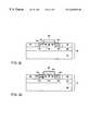
- FIGS. 2 a - 2 kschematically illustrate a series of process steps for fabricating the transistors of FIG. 1 .
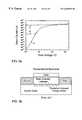
- FIG. 3 ashows computer simulations of the current-versus-voltage (I-V) characteristics of a conventional n-channel SOI field-effect transistor in response to various doses of ionizing radiation.
- FIG. 3 bschematically illustrates the formation of a back-channel leakage conduction path that is formed in the conventional transistor of FIG. 3 a at high irradiation levels.
- FIG. 4 ashows computer simulations of the I-V characteristics of a radiation-hardened n-channel SOI field-effect transistor formed according to the present invention.
- FIG. 4 bschematically illustrates that no back-channel leakage conduction path is formed with the n-channel SOI transistor of FIG. 4 a even though a back-channel inversion layer is generated at high irradiation levels.
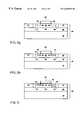
- the present inventioncan be used to form an IC 10 comprised of complementary pairs of n-channel SOI field-effect transistors 12 and p-channel SOI field-effect transistors 14 as shown in the schematic cross-section representation in FIG. 1 .
- Additional circuit elementssuch as resistors and capacitors (not shown in FIG. 1) can also be used to form the IC 10 in combination with the transistors 12 and 14 .
- the SOI field-effect transistors 12 and 14 of the present inventionare different from conventional devices in two important respects that improve their radiation hardness and reduce floating body effects: (1) the source 52 of the transistors 12 and 14 of the present invention does not extend completely through the device layer 22 ; and (2) next to the source 52 is provided a heavily-doped body tie contact 56 that extends partially or completely through the device layer 22 and electrically connects to a body or channel region under the source 52 .
- the transistors 12 and 14 of the present inventioncan be termed as “Body Under Source FETs” or BUSFETs.
- the transistors 12 and 14are formed on an SOI wafer 16 which comprises a substrate 18 of monocrystalline silicon upon which is disposed an electrically insulating buried oxide layer 20 comprising silicon dioxide (SiO 2 ), and a monocrystalline silicon device layer 22 above the layer 20 .
- SOI wafers 16are commercially available, and can be formed by different methods including a separation by implantation of oxygen (SIMOX) process and a wafer bonding process. With the present invention, specially-hardened SOI wafers are not required, thereby reducing cost and increasing wafer availability.
- the SOI wafer 16has a total thickness of generally less than one millimeter, with the device layer 22 typically being up to 500 nanometers thick, and with the buried oxide layer 20 being, for example, about 100-400 nanometers thick.
- FIG. 2 ashows the formation of a patterned mask layer 24 blanketing the device layer 22 of the SOI wafer 16 in preparation for etching a trench 26 down through the device layer 22 to form an isolation region about an island 28 wherein the n-channel SOI field-effect transistor 12 is to be formed, thereby electrically isolating the transistor 12 from the remainder of the device layer 22 .
- Islands 28 used for forming p-channel SOI transistors 14can be formed in the same step.
- a field oxide 30(e.g. SiO 2 or a silicate glass) can be formed in the trench 26 (e.g. by thermal oxidation of the silicon surrounding the trench 26 ) or deposited therein to fill up the trench 26 to planarize the wafer 16 .
- the field oxide 30electrically isolates each island 28 from the remainder of the device layer 22 ; whereas the buried oxide layer 20 electrically isolates each island 28 from the underlying silicon substrate 18 . Any of the field oxide 30 extending above the device layer 22 can be removed by etching, or by chemical-mechanical polishing to planarize the wafer 16 .
- the island 28can be uniformly doped to a dopant concentration of, for example, 10 17 -10 18 cm ⁇ 3 .
- An alternate method for doping the island 28is to use a retrograde doping profile wherein the island dopant concentration is increased with depth from about 10 17 cm ⁇ 3 at the top of the island 28 to about 10 18 cm ⁇ 3 or more at a back-channel interface 36 of the island 28 with the underlying buried oxide layer 20 .
- This retrograde doping profilecan be achieved by initially uniformly ion implanting the island 28 to about 10 17 cm ⁇ 3 and then providing an additional ion implant in the island 28 near the interface 36 with the buried oxide layer 20 to increase the dopant concentration at this location to about 10 18 cm ⁇ 3 or more after thermal activation.
- the use of a retrograde doping profileis advantageous for further increasing the total-dose hardness that can be obtained in the transistors, 12 and 14 , by minimizing the depth of a depletion region at the back-channel interface 36 to aid in prevention of the formation of a conducting path between the source 52 and drain 54 near the back-channel interface 36 .
- high doping at the bottom of the island 28 near the interface 36will improve the effectiveness of the body tie formed by a portion of the doped island 28 underlying the source 52 acting in combination with a body tie contact 56 .
- the goal hereis to provide a doping level that is as high as possible without causing junction breakdown. Additional masking and ion implantation steps can be used for n-type doping of particular islands 28 reserved for p-channel transistors 14 to similar dopant concentrations and profiles using arsenic or phosphorous as the n-type dopant.
- a transistor gate 38is formed over a central portion of the island 28 .
- Thiscan be done by forming a thin thermal oxide 40 comprising about 5-15 nanometers thickness of silicon dioxide on an upper surface of the island 28 , and then depositing and patterning a polysilicon (i.e. polycrystalline silicon) layer 42 over the thermal oxide 40 .
- the thermal oxidecan be formed using a conventional oxidation process (e.g. by exposing the wafer to a dry oxygen ambient at 900° C. for one-half hour).
- the polysilicon layer 42can be deposited by low-pressure chemical vapor deposition (LPCVD) at a temperature of about 580° C.
- the gate 38can be rectangular in shape with a length of, for example, 0.1-2 ⁇ m and a width of, for example, 0.75-10 ⁇ m to form transistors 12 and 14 operating at a voltage of 1-5 volts.
- FIGS. 2 f - 2 ia series of process steps are used to form a drain region 44 and a source region 46 in the island 28 on opposite sides of the gate 38 .
- lightly-doped regions 48are ion implanted into the drain and source regions, 44 and 46 , respectively to reduce the electric field and thereby reduce hot carrier effects.
- the lightly-doped regions 48extend only partially through the thickness of the device layer 22 .
- the depth of the lightly-doped regions 48is preferably about 90 nanometers (i.e. about one-half the thickness of the device layer 22 ).
- arsenicis preferably used as the n-type dopant to form the n-type lightly-doped regions 48 for each n-channel transistor 12 .
- the arseniccan be ion implanted at an energy of, for example, 30 keV and a dose of about 10 13 cm ⁇ 2 to provide a dopant concentration after thermal activation in the range of 5 ⁇ 10 18 -1 ⁇ 10 19 cm ⁇ 3 .
- a p-type dopantsuch as boron can be ion implanted to a similar dose, thereby forming p-type lightly-doped regions 48 on opposite sides of the gate 38 .
- a sidewall spacer 50is preferably formed on each side of the gate 38 above the device layer 22 and above the lightly-doped regions 48 .
- the sidewall spacers 50can be formed by blanket depositing about 100 nanometers of silicon nitride (e.g. by LPCVD) or silicon dioxide over the SOI wafer 16 , and then removing a horizontally-disposed portion of the deposited material by anisotropic dry etching (e.g. reactive ion etching) to leave a vertically-disposed portion (i.e. a fillet) that forms the sidewall spacers 50 as shown in FIG. 2 g.
- anisotropic dry etchinge.g. reactive ion etching
- each n-channel transistor 12are implanted with an n-type dopant that substantially overlaps the earlier implant forming the lightly-doped regions 48 .
- the n-type dopant used for this stepis preferably arsenic which can be ion implanted at an ion beam energy of 30 keV and a dose of 2 ⁇ 10 15 cm ⁇ 2 for the example of a 180-nanometer-thick device layer 22 .
- this implantUpon activation, this implant provides a heavy doping level of about 10 20 cm ⁇ 3 extending about half-way through the thickness of the device layer 22 and forming an n+source 52 for the n-channel transistor 12 .
- boroncan be substituted for the arsenic in the above ion implant step.
- an n + drain 54 for each n-channel field-effect transistor 12can be formed using an additional deep implant step wherein an n-type dopant is implanted to laterally overlap the earlier implants in the drain region 44 and to extend completely through the thickness of the device layer 22 .
- arsenicis preferably used as the n-type dopant, and can be ion implanted at an ion beam energy of 100 keV and a dose of 4 ⁇ 10 15 cm ⁇ 3 .
- the doping level in the deep n + drain 54will be about 10 20 cm ⁇ 3 .
- a deep p + drain 54can be similarly formed for each p-channel transistor 14 in the IC 10 , using boron in place of arsenic as the dopant.
- a body tie contact 56is formed for each radiation-hardened field-effect transistor, 12 or 14 .
- the body tie contact 56can comprise an Ohmic contact formed over a portion of the doped island 28 between the source 52 and the adjacent field oxide 30 , with the body tie contact 56 further being electrically connected to the source 52 .
- the body tie contact 56comprises a highly doped region produced by ion implanting an impurity dopant into a region between the source 52 and the adjacent field oxide 30 .
- the body tie contact 56can extend partially or completely through the thickness of the device layer 22 .
- FIG. 2 jshows a body tie contact 56 that extends completely through the island 28 to the underlying buried oxide layer 20 .
- the body tie contact 56electrically connects to the body under the source 52 to form a body tie that maintains an entire active channel of the transistor 12 or 14 at a fixed electrical potential, thereby significantly reducing any voltage drops along the channel caused by high electrical currents due to a high dose-rate pulse of ionizing radiation, or due to a cosmic ray strike near the center of the active channel.
- the body tie contact 56can thus minimize floating body effects which can otherwise make SOI circuit design difficult and result in increased design margins at the expense of circuit speed and power dissipation.
- the body tie contact 56can be small in area so that the combination of the body tie contact 56 and the source 52 occupy about the same space as the drain 54 . The provision of the body tie contact 56 can thus substantially improve the radiation hardness and electrical performance of the SOI field-effect transistor of the present invention as compared to conventional devices.
- a single n-type dopant implant step(e.g. arsenic) can be used to simultaneously form the deep implants for the n + drain 54 of a plurality of n-channel transistors 12 and n + body tie contacts 56 for a plurality of p-channel transistors 14 .
- a single p-type dopant implant step(e.g. arsenic) can be used to simultaneously form the deep implants for the n + drain 54 of a plurality of n-channel transistors 12 and n + body tie contacts 56 for a plurality of p-channel transistors 14 .
- boroncan be used to simultaneously form the deep implants for the p + drain 54 of a plurality of p-channel transistors 14 and p + body tie contacts 56 for a plurality of n-channel transistors 12 .
- the ion beam energycan be adjusted for the above ion implant steps to provide the desired depth of penetration for the ions as recited above.
- the wafer 16can be annealed to activate the implanted dopant ions.
- This annealing stepcan be performed for example by heating the wafer 16 to a temperature of 900° C. for 60 minutes. Alternately, rapid thermal annealing can be used to activate the implanted ions.
- titaniumis blanket deposited over the wafer 16 to a layer thickness of about 50 nanometers by sputtering and is then reacted with the underlying silicon in a rapid thermal annealing system to form titanium silicide. Any unreacted titanium (e.g. overlying the sidewall spacers 48 and overlying the titanium silicide) is then removed using a conventional wet etchant for titanium.
- the contact 58 overlying the source 52 and the body tie contact 56 in FIG. 2 kserves to short-circuit these two regions, thereby minimizing any radiation-induced photocurrent generated at a p-n junction formed at the interface between the source 52 and the body tie contact 56 .
- an Ohmic contact 58can be used to form the body tie contact without any need for an ion implanted region 56 .
- each p-channel transistor 14is similar to that described above for the n-channel transistor 12 except that a p-type dopant (e.g. boron) is substituted in each instance for the n-type dopant (e.g. arsenic), and vice versa.
- a p-type dopante.g. boron
- the n-type dopante.g. arsenic
- some implant stepscan be used to simultaneously form elements of both the n-channel transistors 12 and the p-channel transistors 14 . The net result is that a minimum of only two additional mask levels are required beyond that needed for the fabrication of conventional CMOS ICs.
- These two additional mask levelsinclude one for deep n + ion implantation of drains of n-channel transistors 12 and body tie contacts of p-channel transistors 14 , and another for deep p + ion implantation of body tie contacts of n-channel transistors 12 and drains of p-channel transistors 14 .
- FIG. 3 ashows the results of a three-dimensional simulation of a conventional partially-depleted n-channel SOI field-effect transistor with 10 ⁇ m ⁇ 0.35 ⁇ m gate dimensions for operation at 3.3 V.
- These computer simulationsshow the response of this conventional device to various doses of ionizing radiation.
- the total-dose response of a particular transistor structureis calculated after providing a sheet of radiation-induced charge of a predetermined magnitude at the back-channel interface 36 (see FIG. 3 b ) and then determining the effect of this charge sheet on the subthreshold drain current versus gate voltage (I-V) characteristics of the transistor structure.
- the curve labelled “A”corresponds to the calculated response of a conventional transistor to a back-channel interface charge of 10 12 cm ⁇ 2 which, in the simulation, can be generated by 3.4 kilorad (SiO 2 ) of irradiation to the buried oxide layer. It should be noted that 1 kilorad (SiO 2 ) of irradiation generates 8.1 ⁇ 10 15 electron-hole pairs per cubic centimeter within the buried oxide layer. The I-V curve “A” in FIG. 3 a is not noticeably affected by this level of irradiation.
- FIGS. 3 a and 3 bshow that the back-channel leakage current can be high even for relatively low levels of total-dose ionizing irradiation; and this can severely limit the lifetime of conventional SOI integrated circuits in space systems.
- FIG. 4 aComputer simulations for a 10 ⁇ m ⁇ 0.35 ⁇ m n-channel radiation-hardened SOI transistor with a retrograde body doping profile formed according to the present invention are shown in FIG. 4 a .
- the I-V curve labelled “D”is calculated for an interface charge level of 10 13 cm ⁇ 2 corresponding to 34.5 kilorad (SiO 2 ) of irradiation of the buried oxide layer 20 .
- the I-V curve labelled “E”is calculated for an interface charge level of 10 15 cm ⁇ 2 corresponding to 3.45 megarad (SiO 2 ) of irradiation of the layer 20 .
- the I-V curve labelled “F”is calculated for an interface charge level of 10 16 cm ⁇ 2 corresponding to 34.5 megarad (SiO 2 ) of irradiation of the layer 20 . Even at these much higher irradiation levels, no back-channel leakage path is formed so that the transistor drain current is not substantially increased.
- the present inventionit is possible to form an IC 10 having an improved radiation hardness without the need for a specially processed hardened buried oxide layer to minimize radiation-induced back-channel leakage.
- This considerable improvement in radiation hardness according to the present inventionis largely due to the design of the source 52 which extends only about halfway through the thickness of the device layer 22 as shown schematically in FIG. 4 b .
- a back-channel inversion layerexists in the silicon island 28 due to the radiation-induced charge sheet, there is no direct conducting path formed between the source 52 and drain 54 because the source 52 is not deep enough to electrically connect to the inversion layer to form a back-channel leakage path.
- a reverse-biased p-n junctionis formed at an interface between the back-channel inversion layer and the body tie contact, thereby limiting any current conduction at this interface.
- the net resultis an orders-of-magnitude improvement in total-dose radiation hardness according to the present invention as compared with conventional SOI technology.
- the IC 10 in FIG. 1can be completed by depositing and patterning one or more layers of metallization (not shown) to interconnect the various transistors and other elements (e.g. resistors and capacitors). Multiple layers of the interconnect metallization can be separated by dielectric layers (not shown), and a final passivation layer (not shown) can be provided to blanket the device 10 for environmental protection. The completed IC 10 can then be packaged for use.
- the SOI field-effect transistors 12 and 14 and the IC 10 formed therefrompresent numerous advantages over conventional SOI technology.
- a BUSFET structure for these devicesallows the devices to achieve high total-dose levels of radiation hardness without sacrificing dose-rate or SEU hardness.
- a BUSFET body tie layout of the devices wherein all regions of the channel width are directly electrically connected to the body tiemay result in an even better dose-rate performance and SEU immunity than conventional radiation-hardened SOI devices.
- the present inventionthus provides an ideal solution for space and weapon systems.
- Floating body effectsafflict conventional commercial SOI devices, creating threshold voltage instabilities, hysteresis effects, and reduced device reliability. These instabilities make circuit design difficult using conventional SOI technology, and result in increased design margins at the expense of circuit speed and power dissipation.
- circuit design models that adequately take into account floating body effectsare not available.
- existing body tie structuresconsume large amounts of additional area, and thus are not compatible with advanced high-performance, high-density integrated circuits.
- the present inventionprovides radiation-hardening advantages
- the present inventionalso provides additional advantages in reducing floating body effects.
- Thisprovides the present invention with utility for forming transistors and integrated circuits for applications that do not require radiation hardening.
- the present inventionis expected to be attractive to designers of commercial SOI circuits.
- the body tie design of the present inventioncan address SEU radiation hardness which is becoming of increasing importance for reliability even for commercial applications on earth or in space. Because of the ever-decreasing feature sizes for ICs, these ICs are becoming more prone to single-event upset due to energetic cosmic rays that penetrate the earth's atmosphere and also to energetic particles generated during processing and packaging.
- the present inventionprovides an improvement in SEU hardness that addresses these concerns and can provide an increased reliability for both commercial and military ICs, thereby reducing the incidence of “soft errors” in the ICs.
Landscapes
- Thin Film Transistor (AREA)
Abstract
Description
This invention was made with Government support under Contract No. DE-AC04-94AL85000 awarded by the U.S. Department of Energy. The Government has certain rights in the invention.
The present invention relates in general to silicon-on-insulator (SOI) devices, and in particular to radiation-hardened SOI field-effect transistors (FETs) for integrated circuits (ICs), and to a method for manufacturing the same.
Silicon-on-insulator (SOI) integrated-circuit (IC) technology offers performance advantages over bulk-silicon or epitaxial-silicon IC technologies for commercial and military applications. SOI ICs can operate at higher speeds and lower power levels than equivalent bulk-silicon ICs, making the SOI ICs particularly useful for mobile communication and high-speed computer applications. These SOI ICs are also less prone to single-event upset (SEU) due to energetic cosmic particles which is important for deployment in outer space, in high-altitude aircraft, or in terrestrial systems.
Single-event upset can lead to system performance degradation or failure in space systems, and is becoming an increasing system reliability concern even in terrestrial systems. To SEU-harden bulk-silicon ICs to high cosmic ray levels, performance-degrading and/or area-degrading radiation hardening techniques must be currently used. Thus, SEU-hardened bulk-silicon ICs may not be compatible with future advanced complementary-metal-oxide-semiconductor (CMOS) technologies.
Silicon-on-insulator ICs can also function without upset or failure after exposure to extremely high dose-rate pulses of ionizing radiation. It is impossible to fabricate bulk-silicon ICs that can function at radiation dose levels achievable by properly designed SOI ICs. These radiation-hardness properties make SOI devices attractive for space and weapon applications. Because of the high levels of SEU and dose-rate radiation hardness obtainable by SOI circuits, system applications heretofore unimaginable with bulk-silicon ICs can be realized. However, the total-dose hardening of SOI devices is much more difficult than for bulk-silicon ICs due to a back-channel leakage current resulting from charge trapping in an oxide layer buried below the SOI devices.
The primary factor that leads to the SEU and dose-rate advantages of SOI technology over bulk-silicon technology is that SOI transistors are built in a thin silicon active layer (also termed a device layer) above a buried silicon dioxide (SiO2) layer (also termed a buried oxide layer) rather than in a bulk silicon wafer. The SOI device layer is typically about 50-200 nanometers thick, compared to a thickness of about 725 μm for a bulk silicon wafer. In a conventional thin-film SOI field-effect transistor or complementary field-effect transistor pair (i.e. an inverter), a source region and a drain region are formed to extend completely through the device layer to the buried oxide below. Transistors in a bulk-silicon IC are formed in n-type or p-type wells that have been ion implanted into the wafer. The SEU hardness of an IC can be related to the charge collected after a cosmic-ray strike. For a bulk-silicon CMOS transistor, charge can be collected from a region several microns deep in the silicon wafer. On the other hand, for an SOI transistor, only the charge deposited within the very thin device layer is collected since the buried oxide layer electrically isolates the device layer from the remainder of the wafer. This provides a higher degree of SEU hardness for SOI devices than for bulk-silicon devices. Furthermore, the dose-rate hardness of an SOI device is superior to a bulk-silicon device since the SOI device has considerably less p-n junction area than the bulk-silicon device because the dose-rate hardness of an IC is related to the total p-n junction area of the IC.
Despite the inherent dose-rate and SEU hardness advantage of SOI technology, two factors can reduce the radiation hardness of SOI circuits. These two factors are floating body effects that degrade SEU and dose-rate hardness, and back-channel leakage that degrades total-dose ionizing radiation hardness. For a partially-depleted SOI transistor, the silicon depletion region does not extend completely through the device layer so that a thin silicon body region exists between the edge of the silicon depletion region and the silicon/buried oxide interface and between the source and drain of the transistor. In normal operation of the SOI transistor as a three-terminal device, this silicon body region is not tied to a specific electrical potential, but is instead floating. Thus, any charge generated within the body region by a cosmic ray strike can cause a reduction in a potential barrier between the source and the body region (i.e. a source-to-body potential). Similarly, electrical charge generated by impact ionization due to an increased current flow as a result of exposure to a high dose-rate pulse of ionizing radiation can cause a reduction in the source-to-body potential. As a result, a parasitic bipolar transistor effect can be initiated that can significantly increase the collected electrical charge. The magnitude of floating body effects can be sufficient to cause reliability degradation due to soft errors in conventional SOI transistors due to terrestrial cosmic rays. To prevent such floating body effects, body ties can be used to tie or electrically connect the body potential to a fixed electrical potential, generally at the same potential as the transistor source. Unfortunately, these body ties can significantly increase the size of the transistors so that most commercial SOI circuit designs use body ties only at critical locations.
The total-dose hardening of SOI ICs is more difficult than hardening bulk-silicon ICs due to the presence of the SOI buried oxide layer. Total-dose ionizing radiation-induced back-channel leakage occurs as positive electrical charge is trapped in the buried oxide near the bottom silicon/buried oxide interface. Typical SOI buried oxides contain numerous defects that result in considerable radiation-induced charge trapping. As charge is trapped in the buried oxide, the overlying silicon becomes inverted at the silicon/buried oxide interface, thereby forming a back-channel leakage current path between the transistor source and drain (see FIG. 3b). The back-channel leakage current can be substantial even at low levels of total-dose ionizing irradiation (see FIG. 3a), and can severely limit the lifetime of conventional SOI ICs in space systems. Techniques have been developed to fabricate hardened SOI buried oxides to minimize radiation-induced positive charge buildup near the back-channel interface. Unfortunately, the present processing techniques used to fabricate radiation hardened buried oxides are expensive to implement, are difficult to control, and are not compatible with standard IC processing equipment.
An advantage of the present invention is that a radiation-hardened SOI field-effect transistor can be fabricated with a significantly reduced radiation-induced back-channel leakage current, while retaining the SEU and dose-rate hardness advantages inherent to thin-film SOI technology.
A further advantage of the present invention is that the SOI field-effect transistor can be formed with a body tie contact extending along an entire conducting channel of the transistor, thereby reducing floating body effects during operation of the transistor.
Yet another advantage of the SOI field-effect transistor having the body tie contact is that the body tie contact can be formed without a significant increase in the area of the transistor.
Still another advantage of the SOI field-effect transistor having the body tie contact is that the body tie contact improves radiation hardening of the transistor, and in particular the single-event-upset hardening of the transistor.
A further advantage is that the SOI field-effect transistor of the present invention provides an improvement over conventional SOI transistors for terrestrial applications (e.g. consumer applications) as well as for space applications.
Yet another advantage of the present invention is that a radiation-hardened SOI integrated circuit can be fabricated comprising one or more complementary pairs of SOI field-effect transistors.
Still another advantage is that the SOI field-effect transistor of the present invention can be formed using a conventional SOI wafer without the need for a SOI wafer having a specially prepared hardened buried oxide layer.
A further advantage of the present invention is that the SOI field-effect transistor of the present invention has an improved radiation hardness to provide a prolonged lifetime in harsh environments.
These and other advantages of the present invention will become evident to those skilled in the art.
The present invention relates to a semiconductor field-effect transistor formed on a silicon-on-insulator wafer, and to a method for fabricating the same. The invention provides an improvement in both electrical characteristics and radiation hardness as compared with conventional SOI FETs.
The semiconductor field-effect transistor comprises an SOI wafer having a monocrystalline silicon substrate, an insulating layer of silicon dioxide overlying the silicon substrate, and a monocrystalline silicon device layer (generally up to 500 nanometers thick) overlying the insulating layer; a gate formed above the device layer; a drain formed on one side of the gate in the device layer and extending completely through the device layer; a source formed on the other side of the gate in the device layer and extending only partially through the device layer (e.g. about halfway); and a body tie contact formed adjacent to the source and electrically connected to the source. In some embodiments of the present invention, the body tie contact can comprise an Ohmic contact; whereas in other embodiments of the present invention, the body tie contact can comprise an ion implanted region that extends either partially or completely through the device layer. The electrical connection between the body tie contact and the source can be provided by a source contact; and the SOI FET can further include electrical contacts to the drain and gate. In the SOI FET, the gate preferably comprises a layer of polysilicon overlying a layer of silicon dioxide. Additionally, a sidewall spacer comprising silicon nitride or silicon dioxide is preferably provided on opposite sides of the gate above the drain and source.
The SOI FET can further include an isolation region formed about the transistor to electrically isolate the transistor from the remainder of the device layer, and from any other transistors formed in the device layer. The isolation region preferably comprises a trench filled with a field oxide that surrounds the transistor.
In the SOI FET, a region of the device layer between the source and drain (i.e. a body region) is doped by ion implantation with ions of a first conductivity type; whereas the drain and source are doped with ions of a second conductivity type. The region of the device layer between the source and drain can further have a retrograde doping profile. The body tie contact can also be doped by ion implantation with ions of the first conductivity type.
The electrical contacts to the SOI FET comprise a metal or metal alloy, preferably a metal silicide, and most preferably titanium silicide. Complementary pairs of transistors can be fabricated according to the present invention for use in forming an integrated circuit.
The body tie contact acts in combination with a region underneath the source to form a body tie which improves electrical characteristics of the device. Additionally, the SOI FET of the present invention provides a high level of radiation hardness.
The method for forming the SOI FET comprises steps for forming an island within a device layer of the wafer at a location wherein the field-effect transistor is to be formed, with the island being doped with ions of a first conductivity type and electrically isolated from the remainder of the device layer; forming a transistor gate over the island; forming a transistor drain on one side of the gate by implanting ions of a second conductivity type into the device layer with the implanted ions extending completely through the device layer; forming a transistor source on the other side of the gate by implanting ions of the second conductivity type into the device layer with the implanted ions extending only partially (e.g. half-way) through the device layer; forming a body tie contact adjacent to the source and electrically connected to the source, with the body tie contact acting in combination with a portion of the doped island underlying the source to form a body tie to improve performance of the device.
The method can further include a step for forming a sidewall spacer on opposite sides of the gate above the drain and source, with the sidewall spacer comprising a deposited and patterned layer of silicon nitride or silicon dioxide. Additionally, the method preferably includes an annealing step for activating the implanted ions.
According to the present invention, the step for forming the island within the device layer preferably comprises etching a trench into the device layer surrounding a region wherein the transistor is to be formed, and filling the trench with an electrically-insulating material. The step for forming the transistor gate preferably comprises forming a silicon dioxide layer over the device layer, depositing a polysilicon layer over the silicon dioxide layer, and patterning the polysilicon layer. The step for forming the transistor drain preferably comprises a plurality of implants of ions at different energies. The step for forming the transistor source preferably comprises implanting ions to a depth that is preferably equal to about one-half the thickness of the device layer, with the device layer generally being about less than 500 nanometers thick, and preferably in the range of 50-200 nanometers thick. The step for forming the body tie contact can include forming an Ohmic contact or alternately implanting ions of the first conductivity type into the device layer with the implanted ions extending partially or completely through the device layer. The method can further include a step for forming electrical contacts to the drain, source and gate, with the source contact further electrically connecting the body tie contact to the source.
Additional advantages and novel features of the invention will become apparent to those skilled in the art upon examination of the following detailed description thereof when considered in conjunction with the accompanying drawings. The advantages of the invention can be realized and attained by means of the instrumentalities and combinations particularly pointed out in the appended claims.
The accompanying drawings, which are incorporated into and form a part of the specification, illustrate several aspects of the present invention and, together with the description, serve to explain the principles of the invention. The drawings are only for the purpose of illustrating preferred embodiments of the invention and are not to be construed as limiting the invention. In the drawings:
FIG. 1 schematically illustrates a cross-section view of a complementary pair of radiation-hardened SOI field-effect transistors formed according to the present invention.
FIGS. 2a-2kschematically illustrate a series of process steps for fabricating the transistors of FIG.1.
FIG. 3ashows computer simulations of the current-versus-voltage (I-V) characteristics of a conventional n-channel SOI field-effect transistor in response to various doses of ionizing radiation.
FIG. 3bschematically illustrates the formation of a back-channel leakage conduction path that is formed in the conventional transistor of FIG. 3aat high irradiation levels.
FIG. 4ashows computer simulations of the I-V characteristics of a radiation-hardened n-channel SOI field-effect transistor formed according to the present invention.
FIG. 4bschematically illustrates that no back-channel leakage conduction path is formed with the n-channel SOI transistor of FIG. 4aeven though a back-channel inversion layer is generated at high irradiation levels.
The present invention relates to a body-tied partially-depleted SOI transistor structure that is hardened to total-dose ionizing irradiation and that maintains the high dose-rate and SEU hardness levels intrinsic to SOI technology and to a method for fabricating the same. The present invention also provides electrical performance advantages over conventional SOI transistors so that the present invention can also be useful for terrestrial applications wherever transistors or integrated circuits (ICs) are used.
The present invention can be used to form anIC 10 comprised of complementary pairs of n-channel SOI field-effect transistors 12 and p-channel SOI field-effect transistors 14 as shown in the schematic cross-section representation in FIG.1. Additional circuit elements such as resistors and capacitors (not shown in FIG. 1) can also be used to form theIC 10 in combination with thetransistors
The SOI field-effect transistors source 52 of thetransistors device layer 22; and (2) next to thesource 52 is provided a heavily-dopedbody tie contact 56 that extends partially or completely through thedevice layer 22 and electrically connects to a body or channel region under thesource 52. Thetransistors
An advantage of limiting the depth of thesource 52 according to the present invention is that the effects of radiation-induced back-channel leakage in thetransistors source 52 and drain54 in thetransistors channel interface 36 is inverted by charge trapped in an underlyingburied oxide layer 20 due to total-dose ionizing irradiation. This substantially improves the radiation hardness of the transistors of the present invention to total-dose ionizing irradiation as compared with conventional SOI transistors. Furthermore, the channel region under thesource 52 is also used in combination with thebody tie contact 56 to form an effective body tie for thetransistors
In FIG. 1, thetransistors SOI wafer 16 which comprises asubstrate 18 of monocrystalline silicon upon which is disposed an electrically insulating buriedoxide layer 20 comprising silicon dioxide (SiO2), and a monocrystallinesilicon device layer 22 above thelayer 20.SOI wafers 16 are commercially available, and can be formed by different methods including a separation by implantation of oxygen (SIMOX) process and a wafer bonding process. With the present invention, specially-hardened SOI wafers are not required, thereby reducing cost and increasing wafer availability. TheSOI wafer 16 has a total thickness of generally less than one millimeter, with thedevice layer 22 typically being up to 500 nanometers thick, and with the buriedoxide layer 20 being, for example, about 100-400 nanometers thick.
FIGS. 2a-2kare schematic cross-section representation views of an n-channel transistor 12 during fabrication. Although the method of the present invention will be described in terms of fabrication of a single n-channel transistor 12, it will be understood by those skilled in the art that a plurality of both n-channel and p-channel transistors can be formed simultaneously on thesame wafer 16 using the same or similar process steps. Furthermore, the fabrication of an integrated circuit (IC) comprising a plurality of n-channel transistors 12 and p-channel transistors 14 can require up to hundreds of individual process steps. Therefore, only the relevant process steps for the present invention will be described herein in detail since those skilled in the art understand other conventional IC processing steps such as photolithography, masking, etching, mask stripping, cleaning, metallization and deposition of dielectric and passivation layers.
FIG. 2ashows the formation of a patternedmask layer 24 blanketing thedevice layer 22 of theSOI wafer 16 in preparation for etching atrench 26 down through thedevice layer 22 to form an isolation region about anisland 28 wherein the n-channel SOI field-effect transistor 12 is to be formed, thereby electrically isolating thetransistor 12 from the remainder of thedevice layer 22.Islands 28 used for forming p-channel SOI transistors 14 can be formed in the same step.
In FIG. 2b, atrench 26 can be etched through thedevice layer 22 to form eachisland 28 and to isolate thatisland 28 from the remainder of thedevice layer 22. This is preferably done using a dry etching process such as reactive ion etching. Thetrench 26 can extend completely through thedevice layer 22 as shown in FIG. 2b; or alternately thetrench 26 can extend most of the way through thedevice layer 22, with the underlying silicon then being thermally oxidized for conversion to silicon dioxide.
In FIG. 2c, a field oxide30 (e.g. SiO2or a silicate glass) can be formed in the trench26 (e.g. by thermal oxidation of the silicon surrounding the trench26) or deposited therein to fill up thetrench 26 to planarize thewafer 16. Thefield oxide 30 electrically isolates eachisland 28 from the remainder of thedevice layer 22; whereas the buriedoxide layer 20 electrically isolates eachisland 28 from theunderlying silicon substrate 18. Any of thefield oxide 30 extending above thedevice layer 22 can be removed by etching, or by chemical-mechanical polishing to planarize thewafer 16.
In FIG. 2d, apatterned implant mask 32 is formed over thewafer 16 with an opening through to theisland 28. P-type dopant ions34 (e.g. boron) are then ion implanted into theisland 28 to dope the island p-type for forming an n-channel transistor 12. Alternately, this step can be performed before thetrench 26 is etched.
In FIG. 2d, theisland 28 can be uniformly doped to a dopant concentration of, for example, 1017-1018cm−3. An alternate method for doping theisland 28 is to use a retrograde doping profile wherein the island dopant concentration is increased with depth from about 1017cm−3at the top of theisland 28 to about 1018cm−3or more at a back-channel interface 36 of theisland 28 with the underlying buriedoxide layer 20. This retrograde doping profile can be achieved by initially uniformly ion implanting theisland 28 to about 1017cm−3and then providing an additional ion implant in theisland 28 near theinterface 36 with the buriedoxide layer 20 to increase the dopant concentration at this location to about 1018cm−3or more after thermal activation. The use of a retrograde doping profile is advantageous for further increasing the total-dose hardness that can be obtained in the transistors,12 and14, by minimizing the depth of a depletion region at the back-channel interface 36 to aid in prevention of the formation of a conducting path between thesource 52 and drain54 near the back-channel interface 36. Also, high doping at the bottom of theisland 28 near theinterface 36 will improve the effectiveness of the body tie formed by a portion of the dopedisland 28 underlying thesource 52 acting in combination with abody tie contact 56. The goal here is to provide a doping level that is as high as possible without causing junction breakdown. Additional masking and ion implantation steps can be used for n-type doping ofparticular islands 28 reserved for p-channel transistors 14 to similar dopant concentrations and profiles using arsenic or phosphorous as the n-type dopant.
In FIG. 2eatransistor gate 38 is formed over a central portion of theisland 28. This can be done by forming a thinthermal oxide 40 comprising about 5-15 nanometers thickness of silicon dioxide on an upper surface of theisland 28, and then depositing and patterning a polysilicon (i.e. polycrystalline silicon)layer 42 over thethermal oxide 40. The thermal oxide can be formed using a conventional oxidation process (e.g. by exposing the wafer to a dry oxygen ambient at 900° C. for one-half hour). Thepolysilicon layer 42 can be deposited by low-pressure chemical vapor deposition (LPCVD) at a temperature of about 580° C. Thegate 38 can be rectangular in shape with a length of, for example, 0.1-2 μm and a width of, for example, 0.75-10 μm to formtransistors
In FIGS. 2f-2i, a series of process steps are used to form adrain region 44 and asource region 46 in theisland 28 on opposite sides of thegate 38.
In FIG. 2f, lightly-dopedregions 48 are ion implanted into the drain and source regions,44 and46, respectively to reduce the electric field and thereby reduce hot carrier effects. The lightly-dopedregions 48 extend only partially through the thickness of thedevice layer 22. For example, if thedevice layer 22 has a thickness of 180 nanometers, the depth of the lightly-dopedregions 48 is preferably about 90 nanometers (i.e. about one-half the thickness of the device layer22). In this example, arsenic is preferably used as the n-type dopant to form the n-type lightly-dopedregions 48 for each n-channel transistor 12. The arsenic can be ion implanted at an energy of, for example, 30 keV and a dose of about 1013cm−2to provide a dopant concentration after thermal activation in the range of 5×10¹⁸-1×1019cm−3. To form each p-channel transistor 14, a p-type dopant such as boron can be ion implanted to a similar dose, thereby forming p-type lightly-dopedregions 48 on opposite sides of thegate 38.
In FIG. 2g, asidewall spacer 50 is preferably formed on each side of thegate 38 above thedevice layer 22 and above the lightly-dopedregions 48. The sidewall spacers50 can be formed by blanket depositing about 100 nanometers of silicon nitride (e.g. by LPCVD) or silicon dioxide over theSOI wafer 16, and then removing a horizontally-disposed portion of the deposited material by anisotropic dry etching (e.g. reactive ion etching) to leave a vertically-disposed portion (i.e. a fillet) that forms thesidewall spacers 50 as shown in FIG. 2g.
In FIG. 2h, the drain and source regions,44 and46, of each n-channel transistor 12 are implanted with an n-type dopant that substantially overlaps the earlier implant forming the lightly-dopedregions 48. This can be done using the same photomask previously used for forming the lightly-dopedregions 48. The n-type dopant used for this step is preferably arsenic which can be ion implanted at an ion beam energy of 30 keV and a dose of 2×1015cm−2for the example of a 180-nanometer-thick device layer 22. Upon activation, this implant provides a heavy doping level of about 1020cm−3extending about half-way through the thickness of thedevice layer 22 and forming an n+source 52 for the n-channel transistor 12. To form a p+ source52 for each p-channel transistor 14, boron can be substituted for the arsenic in the above ion implant step.
In FIG. 2i, an n+ drain54 for each n-channel field-effect transistor 12 can be formed using an additional deep implant step wherein an n-type dopant is implanted to laterally overlap the earlier implants in thedrain region 44 and to extend completely through the thickness of thedevice layer 22. For this step, arsenic is preferably used as the n-type dopant, and can be ion implanted at an ion beam energy of 100 keV and a dose of 4×1015cm−3. Upon activation, the doping level in the deep n+ drain54 will be about 1020cm−3. A deep p+ drain54 can be similarly formed for each p-channel transistor 14 in theIC 10, using boron in place of arsenic as the dopant.
In FIG. 2j, abody tie contact 56 is formed for each radiation-hardened field-effect transistor,12 or14. In some embodiments of the present invention, thebody tie contact 56 can comprise an Ohmic contact formed over a portion of the dopedisland 28 between thesource 52 and theadjacent field oxide 30, with thebody tie contact 56 further being electrically connected to thesource 52. In other embodiments of the present invention as shown in FIGS. 1-2, thebody tie contact 56 comprises a highly doped region produced by ion implanting an impurity dopant into a region between thesource 52 and theadjacent field oxide 30. Thebody tie contact 56 can extend partially or completely through the thickness of thedevice layer 22. FIG. 2jshows abody tie contact 56 that extends completely through theisland 28 to the underlying buriedoxide layer 20.
Thebody tie contact 56 electrically connects to the body under thesource 52 to form a body tie that maintains an entire active channel of thetransistor body tie contact 56 can thus minimize floating body effects which can otherwise make SOI circuit design difficult and result in increased design margins at the expense of circuit speed and power dissipation. Furthermore, thebody tie contact 56 can be small in area so that the combination of thebody tie contact 56 and thesource 52 occupy about the same space as thedrain 54. The provision of thebody tie contact 56 can thus substantially improve the radiation hardness and electrical performance of the SOI field-effect transistor of the present invention as compared to conventional devices.
For an n-channel transistor 12 with an ion implantedbody tie contact 56 as shown in FIG. 2j, a high p+ doping level of about 1020cm−3is used. This high p+ doping level can be achieved using a boron implant at an energy of 30 keV and 2×1015cm−2dose for the example of a 180-nanometer-thick device layer 22. For a p-channel transistor 14, arsenic can be implanted to form thebody tie contact 56.
It should be noted that, when thebody tie contact 56 extends to the underlying buriedoxide layer 20 as shown in FIGS. 1 and 2j, a single n-type dopant implant step (e.g. arsenic) can be used to simultaneously form the deep implants for the n+ drain54 of a plurality of n-channel transistors 12 and n+body tie contacts 56 for a plurality of p-channel transistors 14. Similarly, in the example of FIGS. 1 and 2j, a single p-type dopant implant step (e.g. boron) can be used to simultaneously form the deep implants for the p+ drain54 of a plurality of p-channel transistors 14 and p+body tie contacts 56 for a plurality of n-channel transistors 12. For adevice layer 22 of a different layer thickness from the above example, the ion beam energy can be adjusted for the above ion implant steps to provide the desired depth of penetration for the ions as recited above.
After the various ion implantation steps are performed, thewafer 16 can be annealed to activate the implanted dopant ions. This annealing step can be performed for example by heating thewafer 16 to a temperature of 900° C. for 60 minutes. Alternately, rapid thermal annealing can be used to activate the implanted ions.
In FIG. 2k,electrical contacts 58 are formed over thegate 38,source 52 and drain54 of each transistor,12 and14. Although theelectrical contacts 58 can comprise any deposited or sputtered metal or metal alloy conventionally used for ICs (e.g. aluminum, or copper, or an alloy of aluminum or copper), theelectrical contacts 58 according to a preferred embodiment of the present invention comprise a metal silicide (e.g. cobalt silicide or titanium silicide), and preferably titanium silicide. The titanium silicide can be formed by a self-aligned silicide process (termed “SALICIDE”). In this process, titanium is blanket deposited over thewafer 16 to a layer thickness of about 50 nanometers by sputtering and is then reacted with the underlying silicon in a rapid thermal annealing system to form titanium silicide. Any unreacted titanium (e.g. overlying thesidewall spacers 48 and overlying the titanium silicide) is then removed using a conventional wet etchant for titanium.
Thecontact 58 overlying thesource 52 and thebody tie contact 56 in FIG. 2kserves to short-circuit these two regions, thereby minimizing any radiation-induced photocurrent generated at a p-n junction formed at the interface between thesource 52 and thebody tie contact 56. As described previously, in some instances, anOhmic contact 58 can be used to form the body tie contact without any need for an ion implantedregion 56.
The process for forming each p-channel transistor 14 is similar to that described above for the n-channel transistor 12 except that a p-type dopant (e.g. boron) is substituted in each instance for the n-type dopant (e.g. arsenic), and vice versa. As mentioned previously, some implant steps can be used to simultaneously form elements of both the n-channel transistors 12 and the p-channel transistors 14. The net result is that a minimum of only two additional mask levels are required beyond that needed for the fabrication of conventional CMOS ICs. These two additional mask levels include one for deep n+ ion implantation of drains of n-channel transistors 12 and body tie contacts of p-channel transistors 14, and another for deep p+ ion implantation of body tie contacts of n-channel transistors 12 and drains of p-channel transistors 14.
FIG. 3ashows the results of a three-dimensional simulation of a conventional partially-depleted n-channel SOI field-effect transistor with 10 μm×0.35 μm gate dimensions for operation at 3.3 V. These computer simulations show the response of this conventional device to various doses of ionizing radiation. In the computer simulations, the total-dose response of a particular transistor structure is calculated after providing a sheet of radiation-induced charge of a predetermined magnitude at the back-channel interface36 (see FIG. 3b) and then determining the effect of this charge sheet on the subthreshold drain current versus gate voltage (I-V) characteristics of the transistor structure. In reality, charge generated in the buried oxide layer is nonuniformly trapped throughout the buried oxide layer, with the trapping efficiency and charge being dependent on the local electric field within the layer. The computer simulation is simplified by assuming a one-hundred percent trapping efficiency and charge yield, and in further assuming that all of the charge generated by the irradiation is trapped at the back-channel interface, thereby providing a worst-case total accumulated dose irradiation level. The simulations further assume a retrograde body doping profile with a back-channel doping level of 1×1018cm−3, a device layer thickness of 180 nanometers, and a buried oxide layer thickness of 370 nanometers.
In FIG. 3a, the curve labelled “A” corresponds to the calculated response of a conventional transistor to a back-channel interface charge of 1012cm−2which, in the simulation, can be generated by 3.4 kilorad (SiO2) of irradiation to the buried oxide layer. It should be noted that 1 kilorad (SiO2) of irradiation generates 8.1×10¹⁵electron-hole pairs per cubic centimeter within the buried oxide layer. The I-V curve “A” in FIG. 3ais not noticeably affected by this level of irradiation.
However, the I-V characteristics of the conventional transistor are significantly affected by a slight increase in the irradiation dose. This is seen in the calculated curve “B” at an interface charge of 3×1012cm−2corresponding to an irradiation dose of 10.3 kilorad (SiO2) to the buried oxide layer, and more profoundly in the curve “C” at a slightly higher interface charge of 5×1012cm−2corresponding to an irradiation dose of 17.2 kilorad (SiO2). The increased charge for curves “B” and “C” inverts the silicon near the interface and creates a direct back-channel leakage path between the source and drain regions as illustrated by the horizontal arrow in FIG. 3b. This leakage path results in a substantial leakage current conduction at the increased irradiation levels when 3.3 V of bias is applied to the drain in these simulations. FIGS. 3aand3bshow that the back-channel leakage current can be high even for relatively low levels of total-dose ionizing irradiation; and this can severely limit the lifetime of conventional SOI integrated circuits in space systems.
Computer simulations for a 10 μm×0.35 μm n-channel radiation-hardened SOI transistor with a retrograde body doping profile formed according to the present invention are shown in FIG. 4a. The I-V curve labelled “D” is calculated for an interface charge level of 1013cm−2corresponding to 34.5 kilorad (SiO2) of irradiation of the buriedoxide layer 20. The I-V curve labelled “E” is calculated for an interface charge level of 1015cm−2corresponding to 3.45 megarad (SiO2) of irradiation of thelayer 20. Finally, the I-V curve labelled “F” is calculated for an interface charge level of 1016cm−2corresponding to 34.5 megarad (SiO2) of irradiation of thelayer 20. Even at these much higher irradiation levels, no back-channel leakage path is formed so that the transistor drain current is not substantially increased. Thus, according to the present invention it is possible to form anIC 10 having an improved radiation hardness without the need for a specially processed hardened buried oxide layer to minimize radiation-induced back-channel leakage.
This considerable improvement in radiation hardness according to the present invention is largely due to the design of thesource 52 which extends only about halfway through the thickness of thedevice layer 22 as shown schematically in FIG. 4b. Although a back-channel inversion layer exists in thesilicon island 28 due to the radiation-induced charge sheet, there is no direct conducting path formed between thesource 52 and drain54 because thesource 52 is not deep enough to electrically connect to the inversion layer to form a back-channel leakage path. Furthermore a reverse-biased p-n junction is formed at an interface between the back-channel inversion layer and the body tie contact, thereby limiting any current conduction at this interface. The net result is an orders-of-magnitude improvement in total-dose radiation hardness according to the present invention as compared with conventional SOI technology.
TheIC 10 in FIG. 1 can be completed by depositing and patterning one or more layers of metallization (not shown) to interconnect the various transistors and other elements (e.g. resistors and capacitors). Multiple layers of the interconnect metallization can be separated by dielectric layers (not shown), and a final passivation layer (not shown) can be provided to blanket thedevice 10 for environmental protection. The completedIC 10 can then be packaged for use.
As described herein, the SOI field-effect transistors IC 10 formed therefrom present numerous advantages over conventional SOI technology. A BUSFET structure for these devices allows the devices to achieve high total-dose levels of radiation hardness without sacrificing dose-rate or SEU hardness. Furthermore, a BUSFET body tie layout of the devices wherein all regions of the channel width are directly electrically connected to the body tie may result in an even better dose-rate performance and SEU immunity than conventional radiation-hardened SOI devices. The present invention thus provides an ideal solution for space and weapon systems.
Floating body effects afflict conventional commercial SOI devices, creating threshold voltage instabilities, hysteresis effects, and reduced device reliability. These instabilities make circuit design difficult using conventional SOI technology, and result in increased design margins at the expense of circuit speed and power dissipation. Presently, circuit design models that adequately take into account floating body effects are not available. Finally, existing body tie structures consume large amounts of additional area, and thus are not compatible with advanced high-performance, high-density integrated circuits.
Thus, although the present invention provides radiation-hardening advantages, the present invention also provides additional advantages in reducing floating body effects. This provides the present invention with utility for forming transistors and integrated circuits for applications that do not require radiation hardening. Thus, the present invention is expected to be attractive to designers of commercial SOI circuits.
Finally, the body tie design of the present invention can address SEU radiation hardness which is becoming of increasing importance for reliability even for commercial applications on earth or in space. Because of the ever-decreasing feature sizes for ICs, these ICs are becoming more prone to single-event upset due to energetic cosmic rays that penetrate the earth's atmosphere and also to energetic particles generated during processing and packaging. The present invention provides an improvement in SEU hardness that addresses these concerns and can provide an increased reliability for both commercial and military ICs, thereby reducing the incidence of “soft errors” in the ICs.
Other applications and variations of the present invention will become evident to those skilled in the art. The actual scope of the invention is intended to be defined in the following claims when viewed in their proper perspective based on the prior art.
Claims (44)
1. A silicon-on-insulator field-effect transistor, comprising:
(a) a silicon-on-insulator wafer further comprising:
a monocrystalline silicon substrate;
an insulating layer of silicon dioxide overlying the silicon substrate; and
a monocrystalline silicon device layer overlying the insulating layer;
(b) a gate formed above the device layer;
(c) a multiply-doped drain formed on one side of the gate in the device layer and extending completely through the device layer, the drain further comprising a first lightly-doped portion formed with a first width and extending only partially through the device layer, with the first lightly-doped portion partially overlapping and extending laterally beyond a first heavily-doped portion that extends downward completely through the device layer;
(d) a multiply-doped source formed on the other side of the gate in the device layer and extending only partially through the device layer, the source further comprising a second lightly-doped portion and a second heavily-doped portion partially overlapping the second lightly-doped portion; and
(e) a body tie contact formed adjacent to the source and electrically connected to the source.
2. The transistor of claim1 further including a sidewall spacer on opposite sides of the gate above the drain and source.
3. The transistor of claim2 wherein the sidewall spacer comprises silicon nitride or silicon dioxide.
4. The transistor of claim1 wherein the gate comprises a layer of polysilicon overlying a layer of silicon dioxide.
5. The transistor of claim1 wherein a region of the device layer between the source and drain is doped with dopant ions of a first conductivity type, and the drain and source are doped with dopant ions of a second conductivity type.
6. The transistor of claim5 wherein the source extends only about half-way through the device layer.
7. The transistor of claim5 wherein the body tie contact comprises an ion implanted region doped with dopant ions of the first conductivity type and with the ion implanted region extending at least partially through the device layer.
8. The transistor of claim7 wherein the ion implanted region extends completely through the device layer.
9. The transistor of claim1 wherein the body tie contact comprises an Ohmic contact.
10. The transistor of claim1 wherein the device layer has a thickness of up to 500 nanometers.
11. The transistor of claim1 wherein the electrical connection between the body tie contact and the source is provided by a source contact, and further including electrical contacts to the drain and gate.
12. The transistor of claim11 wherein the drain, source and gate contacts comprise a metal or metal alloy.
13. The transistor of claim11 wherein the drain, source and gate contacts comprise a metal silicide.
14. The transistor of claim13 wherein the drain, source and gate contacts comprise titanium silicide.
15. A silicon-on-insulator field-effect transistor, comprising:
(a) a silicon-on-insulator wafer further comprising:
a monocrystalline silicon substrate;
an insulating layer of silicon dioxide overlying the silicon substrate; and
a monocrystalline silicon device layer overlying the insulating layer;
(b) a gate formed above the device layer;
(c) a drain formed on one side of the gate in the device layer and extending completely through the device layer;
(d) a source formed on the other side of the gate in the device layer and extending only partially through the device layer, with a region of the device layer underlying the source and between the source and drain being doped with dopant ions of a first conductivity type to form a retrograde doping profile, and with the drain and source being doped with dopant ions of a second conductivity type;
(e) a body tie contact formed adjacent to the source and electrically connected to the source; and
(f) a sidewall spacer on opposite sides of the gate above the drain and source.
16. The transistor of claim15 wherein the isolation region comprises a trench filled with a silicate glass.
17. The transistor of claim15 wherein the sidewall spacer comprises silicon nitride or silicon dioxide.
18. The transistor of claim15 wherein the gate further comprises a layer of polysilicon overlying a layer of silicon dioxide.
19. The transistor of claim15 wherein a region of the device layer between the source and drain is doped with dopant ions of a first conductivity type, and the drain and source are doped with dopant ions of a second conductivity type.
20. The transistor of claim19 wherein the region of the device layer between the source and drain has a retrograde doping profile.
21. The transistor of claim19 wherein the source extends only about half-way through the device layer.
22. The transistor of claim19 wherein the body tie contact comprises an ion implanted region doped with dopant ions of the first conductivity type and with the ion implanted region extending at least partially through the device layer.
23. The transistor of claim22 wherein the ion implanted region extends completely through the device layer.
24. The transistor of claim15 wherein the body tie contact comprises an Ohmic contact.
25. The transistor of claim15 wherein the device layer has a thickness of up to 500 nanometers.
26. The transistor of claim15 wherein the electrical connection between the body tie contact and the source is provided by a source contact, and further including electrical contacts to the drain and gate.
27. The transistor of claim26 wherein the drain, source and gate contacts comprise a metal or metal alloy.
28. The transistor of claim26 wherein the drain, source and gate contacts comprise a metal silicide.
29. The transistor of claim28 wherein the drain, source and gate contacts comprise titanium silicide.
30. A radiation-hardened silicon-on-insulator field-effect transistor, comprising:
(a) a silicon-on-insulator wafer further comprising:
a monocrystalline silicon substrate;
an insulating layer of silicon dioxide overlying the silicon substrate; and
a monocrystalline silicon device layer overlying the insulating layer;
(b) a gate formed above the device layer;
(c) a multiply-doped drain formed on one side of the gate in the device layer and extending completely through the device layer, the drain further comprising a first lightly-doped portion formed with a first width and extending only partially through the device layer, with the first lightly-doped portion partially overlapping and extending laterally beyond a first heavily-doped portion that extends downward completely through the device layer;
(d) a multiply-doped source formed on the other side of the gate in the device layer and extending only partially through the device layer, the source further comprising a second lightly-doped portion and a second heavily-doped portion partially overlapping the second lightly-doped portion; and
(e) a body tie contact formed adjacent to the source and electrically connected to the source.
31. The radiation-hardened transistor of claim30 further including a sidewall spacer on opposite sides of the gate above the drain and source.
32. The radiation-hardened transistor of claim31 wherein the sidewall spacer comprises silicon nitride or silicon dioxide.
33. The radiation-hardened transistor of claim30 wherein the gate comprises a layer of polysilicon overlying a layer of silicon dioxide.
34. The radiation-hardened transistor of claim30 wherein a region of the device layer between the source and drain is doped with dopant ions of a first conductivity type, and the drain and source are doped with dopant ions of a second conductivity type.
35. The radiation-hardened transistor of claim34 wherein the source extends only about half-way through the device layer.
36. The radiation-hardened transistor of claim34 wherein the body tie contact comprises an ion implanted region doped with dopant ions of the first conductivity type and with the ion implanted region extending at least partially through the device layer.
37. The radiation-hardened transistor of claim36 wherein the ion implanted region extends completely through the device layer.
38. The radiation-hardened transistor of claim30 wherein the body tie contact comprises an Ohmic contact.
39. The radiation-hardened transistor of claim30 wherein the device layer has a thickness of up to 500 nanometers.
40. The radiation-hardened transistor of claim30 wherein the electrical connection between the body tie contact and the source is provided by a source contact, and further including electrical contacts to the drain and gate.
41. The radiation-hardened transistor of claim40 wherein the drain, source and gate contacts comprise a metal or metal alloy.
42. The radiation-hardened transistor of claim40 wherein the drain, source and gate contacts comprise a metal silicide.
43. The radiation-hardened transistor of claim42 wherein the drain, source and gate contacts comprise titanium silicide.
44. A radiation-hardened silicon-on-insulator field-effect transistor, comprising:
(a) a silicon-on-insulator wafer further comprising:
a monocrystalline silicon substrate:
an insulating layer of silicon dioxide overlying the silicon substrate; and
a monocrystalline silicon device laver overlying the insulating layer;
(b) a gate formed above the device layer;
(c) a drain formed on one side of the gate in the device layer and extending completely through the device layer;
(d) a source formed on the other side of the gate in the device layer and extending only partially through the device layer, with a region of the device layer between the source and drain being doped with dopant ions of a first conductivity type to form a retrograde doping profile, and with the drain and source being doped with dopant ions of a second conductivity type; and
(e) a body tie contact formed adjacent to the source and electrically connected to the source.
Priority Applications (1)
| Application Number | Priority Date | Filing Date | Title |
|---|---|---|---|
| US09/270,374US6268630B1 (en) | 1999-03-16 | 1999-03-16 | Silicon-on-insulator field effect transistor with improved body ties for rad-hard applications |
Applications Claiming Priority (1)
| Application Number | Priority Date | Filing Date | Title |
|---|---|---|---|
| US09/270,374US6268630B1 (en) | 1999-03-16 | 1999-03-16 | Silicon-on-insulator field effect transistor with improved body ties for rad-hard applications |
Publications (1)
| Publication Number | Publication Date |
|---|---|
| US6268630B1true US6268630B1 (en) | 2001-07-31 |
Family
ID=23031093
Family Applications (1)
| Application Number | Title | Priority Date | Filing Date |
|---|---|---|---|
| US09/270,374Expired - LifetimeUS6268630B1 (en) | 1999-03-16 | 1999-03-16 | Silicon-on-insulator field effect transistor with improved body ties for rad-hard applications |
Country Status (1)
| Country | Link |
|---|---|
| US (1) | US6268630B1 (en) |
Cited By (60)
| Publication number | Priority date | Publication date | Assignee | Title |
|---|---|---|---|---|
| US6376882B1 (en)* | 2000-05-04 | 2002-04-23 | United Microelectronics Corp. | Electrostatic discharge protection apparatus with silicon control rectifier and the method of fabricating the same |
| US20020113266A1 (en)* | 2001-01-19 | 2002-08-22 | Akihiko Ebina | Semiconductor devices and methods for manufacturing the same |
| US6441434B1 (en) | 2000-03-31 | 2002-08-27 | Advanced Micro Devices, Inc. | Semiconductor-on-insulator body-source contact and method |
| US6472274B1 (en)* | 2000-06-29 | 2002-10-29 | International Business Machines Corporation | MOSFET with self-aligned channel edge implant and method |
| US6525381B1 (en)* | 2000-03-31 | 2003-02-25 | Advanced Micro Devices, Inc. | Semiconductor-on-insulator body-source contact using shallow-doped source, and method |
| US6531738B1 (en)* | 1999-08-31 | 2003-03-11 | Matsushita Electricindustrial Co., Ltd. | High voltage SOI semiconductor device |
| US6531739B2 (en)* | 2001-04-05 | 2003-03-11 | Peregrine Semiconductor Corporation | Radiation-hardened silicon-on-insulator CMOS device, and method of making the same |
| US20030138997A1 (en)* | 2002-01-16 | 2003-07-24 | Zhongze Wang | Methods of forming silicon-on-insulator comprising integrated circuitry, and wafer bonding methods of forming silicon-on-insulator comprising integrated circuitry |
| KR100400717B1 (en)* | 2002-01-16 | 2003-10-08 | 한국전자통신연구원 | Method of manufacturing a nano transistor |
| US20040007744A1 (en)* | 2002-07-12 | 2004-01-15 | Samsung Electronics Co., Ltd. | Semiconductor device having a merged region and method of fabrication |
| US20040021169A1 (en)* | 2002-05-22 | 2004-02-05 | Stmicroelectronics S.R.L. | Integrated structure effective to form a MOS component in a dielectrically insulated well |
| US6693326B2 (en)* | 2000-04-04 | 2004-02-17 | Sharp Kabushiki Kaisha | Semiconductor device of SOI structure |
| US6693329B2 (en) | 2001-01-19 | 2004-02-17 | Seiko Epson Corporation | Semiconductor devices having a field effect transistor and a bi-polar transistor |
| US20040044510A1 (en)* | 2002-08-27 | 2004-03-04 | Zolotov Vladamir P | Fast simulaton of circuitry having soi transistors |
| US6716682B1 (en)* | 2000-08-31 | 2004-04-06 | Micron Technology, Inc. | SOI CMOS device with reduced DIBL |
| US20040084689A1 (en)* | 2002-01-28 | 2004-05-06 | Taiwan Semiconductor Manufacturing Company | Gate-controlled, negative resistance diode device using band-to-band tunneling |
| US6734500B2 (en) | 2000-12-15 | 2004-05-11 | Seiko Epson Corporation | Semiconductor devices including a bi-polar transistor and a field effect transistor |
| US20040152278A1 (en)* | 2000-02-14 | 2004-08-05 | Micron Technology, Inc. | Low dielectric constant STI with SOI devices |
| US6806539B2 (en)* | 2001-06-19 | 2004-10-19 | Sharp Kabushiki Kaisha | Semiconductor device and its manufacturing method |
| US20050006703A1 (en)* | 2001-04-05 | 2005-01-13 | Miscione Anthony M. | Radiation-hardened silicon-on-insulator CMOS device, and method of making the same |
| US20050017289A1 (en)* | 2003-07-24 | 2005-01-27 | Ji-Young Kim | Vertical double-channel silicon-on-insulator transistor and method of manufacturing the same |
| US20050029663A1 (en)* | 2000-02-22 | 2005-02-10 | Micron Technology, Inc. | Polynorbornene foam insulation for integrated circuits |
| US6872640B1 (en) | 2004-03-16 | 2005-03-29 | Micron Technology, Inc. | SOI CMOS device with reduced DIBL |
| US20050205953A1 (en)* | 2004-03-22 | 2005-09-22 | Mitsutoshi Nakamura | Semiconductor device |
| US20060027869A1 (en)* | 2003-07-24 | 2006-02-09 | Samsung Electronics Co., Ltd. | Vertical double-channel silicon-on-insulator transistor and method of manufacturing the same |
| US7009250B1 (en) | 2004-08-20 | 2006-03-07 | Micron Technology, Inc. | FinFET device with reduced DIBL |
| US20060060844A1 (en)* | 2004-09-17 | 2006-03-23 | International Business Machines Corporation | Electrical open/short contact alignment structure for active region vs. gate region |
| US20060060926A1 (en)* | 2004-09-17 | 2006-03-23 | International Business Machines Corporation | Semiconductor scheme for reduced circuit area in a simplified process |
| US20060104095A1 (en)* | 2004-11-15 | 2006-05-18 | Summer Steven E | Method for implementing radiation hardened, power efficient, non isolated low output voltage DC/DC converters with non-radiation hardened components |
| US20060205128A1 (en)* | 2005-03-10 | 2006-09-14 | Micron Technology, Inc. | Integrated circuits and methods of forming a field effect transistor |
| US20060244062A1 (en)* | 2005-04-28 | 2006-11-02 | International Business Machines Corporation | Silicon-on-insulator based radiation detection device and method |
| US20070181882A1 (en)* | 2006-02-09 | 2007-08-09 | Lee Han-Sin | Multi-level semiconductor device and method of fabricating the same |
| US20070195841A1 (en)* | 2006-02-21 | 2007-08-23 | Aitken John M | Charge neutralization in semiconductor structures |
| US20070257310A1 (en)* | 2006-05-02 | 2007-11-08 | Honeywell International Inc. | Body-tied MOSFET device with strained active area |
| US7298010B1 (en)* | 2006-02-21 | 2007-11-20 | Sandia Corporation | Radiation-hardened transistor and integrated circuit |
| US20080044979A1 (en)* | 2006-08-18 | 2008-02-21 | Micron Technology, Inc. | Integrated circuitry, electromagnetic radiation interaction components, transistor devices and semiconductor construction; and methods of forming integrated circuitry, electromagnetic radiation interaction components, transistor devices and semiconductor constructions |
| US7335965B2 (en) | 1999-08-25 | 2008-02-26 | Micron Technology, Inc. | Packaging of electronic chips with air-bridge structures |
| RU2320049C2 (en)* | 2003-06-20 | 2008-03-20 | ГНЦ РФ Государственное учреждение научно-производственный комплекс "Технологический центр" при Московском государственном институте электронной техники /технический университет/ | Method for enhancing radiation resistance of cmos circuit components on soi substrate |
| US20080187463A1 (en)* | 2007-02-07 | 2008-08-07 | Wells David H | Electromagnetic radiation interaction components, fluorimetry systems, semiconductor constructions, and electromagnetic radiation emitter and conduit construction |
| US20080233199A1 (en)* | 2007-03-22 | 2008-09-25 | Alkermes, Inc. | Coacervation Process |
| US20080260847A1 (en)* | 2004-04-15 | 2008-10-23 | Alkermes, Inc. | Polymer-Based Sustained Release Device |
| US20080317865A1 (en)* | 2007-06-20 | 2008-12-25 | Alkermes, Inc. | Quench liquids and washing systems for production of microparticles |
| US20090194894A1 (en)* | 2001-08-31 | 2009-08-06 | Alkermes, Inc. | Residual solvent extraction method and microparticles produced thereby |
| US20090243029A1 (en)* | 2008-03-26 | 2009-10-01 | Anderson Brent A | Method, structure and design structure for customizing history effects of soi circuits |
| US20090242985A1 (en)* | 2008-03-26 | 2009-10-01 | Anderson Brent A | Method, structure and design structure for customizing history effects of soi circuits |
| US20090243000A1 (en)* | 2008-03-26 | 2009-10-01 | Anderson Brent A | Method, structure and design structure for customizing history effects of soi circuits |
| US20100237389A1 (en)* | 2009-03-20 | 2010-09-23 | International Business Machines Corporation | Design structure for heavy ion tolerant device, method of manufacturing the same and structure thereof |
| US20110138735A1 (en)* | 2009-12-11 | 2011-06-16 | The Foley Group, LLC | Connector system for securing an end portion of a steel structural member to a vertical cast concrete member |
| US20110163380A1 (en)* | 2010-01-07 | 2011-07-07 | International Business Machines Corporation | Body-Tied Asymmetric N-Type Field Effect Transistor |
| US20110163379A1 (en)* | 2010-01-07 | 2011-07-07 | International Business Machines Corporation | Body-Tied Asymmetric P-Type Field Effect Transistor |
| US20120132994A1 (en)* | 2010-11-29 | 2012-05-31 | International Business Machines Corporation | High-voltage semiconductor-on-insulator device |
| US8217456B1 (en) | 2011-03-11 | 2012-07-10 | International Business Machines Corporation | Low capacitance hi-K dual work function metal gate body-contacted field effect transistor |
| RU2477904C1 (en)* | 2011-07-25 | 2013-03-20 | Учреждение Российской академии наук Научно-исследовательский институт системных исследований РАН (НИИСИ РАН) | Transistor with metal-oxide-semiconductor structure on silicon-on-insulator substrate |
| CN103700701A (en)* | 2013-12-26 | 2014-04-02 | 杭州电子科技大学 | Silicon on insulator (SOI) process-based back gate drain/source semi-floating front gate P type metal-oxide-semiconductor field effect transistor (P-MOSFET) radio frequency switch zero loss device |
| CN103715263A (en)* | 2013-12-26 | 2014-04-09 | 杭州电子科技大学 | Back grid drain/source self-floating front grid N-MOSFET radio frequency switch zero-loss device based on SOI technology |
| US9401334B1 (en) | 2015-03-13 | 2016-07-26 | International Business Machines Corporation | Preventing unauthorized use of integrated circuits for radiation-hard applications |
| US20160276332A1 (en)* | 2015-03-19 | 2016-09-22 | Freescale Semiconductor, Inc. | Esd protection structure and method of fabrication thereof |
| US9515171B1 (en) | 2015-10-22 | 2016-12-06 | International Business Machines Corporation | Radiation tolerant device structure |
| US9960251B2 (en) | 2015-03-19 | 2018-05-01 | Nxp Usa, Inc. | ESD protection structure and method of fabrication thereof |
| CN114664919A (en)* | 2022-03-14 | 2022-06-24 | 电子科技大学 | Channel heavily doped anti-total dose NMOS device |
Citations (10)
| Publication number | Priority date | Publication date | Assignee | Title |
|---|---|---|---|---|
| US5021359A (en) | 1988-06-21 | 1991-06-04 | Harris Corporation | Radiation hardened complementary transistor integrated circuits |
| US5024965A (en) | 1990-02-16 | 1991-06-18 | Chang Chen Chi P | Manufacturing high speed low leakage radiation hardened CMOS/SOI devices |
| US5137837A (en) | 1990-08-20 | 1992-08-11 | Hughes Aircraft Company | Radiation-hard, high-voltage semiconductive device structure fabricated on SOI substrate |
| US5489792A (en)* | 1994-04-07 | 1996-02-06 | Regents Of The University Of California | Silicon-on-insulator transistors having improved current characteristics and reduced electrostatic discharge susceptibility |
| US5517047A (en)* | 1992-07-28 | 1996-05-14 | Harris Corporation | Bonded wafer processing |
| US5659192A (en) | 1993-06-30 | 1997-08-19 | Honeywell Inc. | SOI substrate fabrication |
| US5760443A (en) | 1993-10-18 | 1998-06-02 | Regents Of The University Of California | Silicon on insulator with active buried regions |
| US5795813A (en) | 1996-05-31 | 1998-08-18 | The United States Of America As Represented By The Secretary Of The Navy | Radiation-hardening of SOI by ion implantation into the buried oxide layer |
| US5808319A (en)* | 1996-10-10 | 1998-09-15 | Advanced Micro Devices, Inc. | Localized semiconductor substrate for multilevel transistors |
| US5807771A (en) | 1996-06-04 | 1998-09-15 | Raytheon Company | Radiation-hard, low power, sub-micron CMOS on a SOI substrate |
- 1999
- 1999-03-16USUS09/270,374patent/US6268630B1/ennot_activeExpired - Lifetime
Patent Citations (10)
| Publication number | Priority date | Publication date | Assignee | Title |
|---|---|---|---|---|
| US5021359A (en) | 1988-06-21 | 1991-06-04 | Harris Corporation | Radiation hardened complementary transistor integrated circuits |
| US5024965A (en) | 1990-02-16 | 1991-06-18 | Chang Chen Chi P | Manufacturing high speed low leakage radiation hardened CMOS/SOI devices |
| US5137837A (en) | 1990-08-20 | 1992-08-11 | Hughes Aircraft Company | Radiation-hard, high-voltage semiconductive device structure fabricated on SOI substrate |
| US5517047A (en)* | 1992-07-28 | 1996-05-14 | Harris Corporation | Bonded wafer processing |
| US5659192A (en) | 1993-06-30 | 1997-08-19 | Honeywell Inc. | SOI substrate fabrication |
| US5760443A (en) | 1993-10-18 | 1998-06-02 | Regents Of The University Of California | Silicon on insulator with active buried regions |
| US5489792A (en)* | 1994-04-07 | 1996-02-06 | Regents Of The University Of California | Silicon-on-insulator transistors having improved current characteristics and reduced electrostatic discharge susceptibility |
| US5795813A (en) | 1996-05-31 | 1998-08-18 | The United States Of America As Represented By The Secretary Of The Navy | Radiation-hardening of SOI by ion implantation into the buried oxide layer |
| US5807771A (en) | 1996-06-04 | 1998-09-15 | Raytheon Company | Radiation-hard, low power, sub-micron CMOS on a SOI substrate |
| US5808319A (en)* | 1996-10-10 | 1998-09-15 | Advanced Micro Devices, Inc. | Localized semiconductor substrate for multilevel transistors |
Non-Patent Citations (1)
| Title |
|---|
| E.P. Ver Ploeg, T. Watanabe, N.A. Kistler, J.C.S. Woo and J.D. Plummer, "Elimination of Bipolar-Induced Breakdown in Fully-Depleted SOI MOSFETs," Technical Digest of the International Electron Devices Meeting, pp. 337-340 (IEEE, 1992). |
Cited By (167)
| Publication number | Priority date | Publication date | Assignee | Title |
|---|---|---|---|---|
| US7387912B2 (en) | 1999-08-25 | 2008-06-17 | Micron Technology, Inc. | Packaging of electronic chips with air-bridge structures |
| US7335965B2 (en) | 1999-08-25 | 2008-02-26 | Micron Technology, Inc. | Packaging of electronic chips with air-bridge structures |
| USRE41368E1 (en)* | 1999-08-31 | 2010-06-08 | Panasonic Corporation | High voltage SOI semiconductor device |
| US6531738B1 (en)* | 1999-08-31 | 2003-03-11 | Matsushita Electricindustrial Co., Ltd. | High voltage SOI semiconductor device |
| US20040152278A1 (en)* | 2000-02-14 | 2004-08-05 | Micron Technology, Inc. | Low dielectric constant STI with SOI devices |
| US6953983B2 (en)* | 2000-02-14 | 2005-10-11 | Micron Technology, Inc. | Low dielectric constant STI with SOI devices |
| US20050029663A1 (en)* | 2000-02-22 | 2005-02-10 | Micron Technology, Inc. | Polynorbornene foam insulation for integrated circuits |
| US6525381B1 (en)* | 2000-03-31 | 2003-02-25 | Advanced Micro Devices, Inc. | Semiconductor-on-insulator body-source contact using shallow-doped source, and method |
| US6441434B1 (en) | 2000-03-31 | 2002-08-27 | Advanced Micro Devices, Inc. | Semiconductor-on-insulator body-source contact and method |
| US6790750B1 (en) | 2000-03-31 | 2004-09-14 | Advanced Micro Devices, Inc. | Semiconductor-on-insulator body-source contact and method |
| US6693326B2 (en)* | 2000-04-04 | 2004-02-17 | Sharp Kabushiki Kaisha | Semiconductor device of SOI structure |
| US6376882B1 (en)* | 2000-05-04 | 2002-04-23 | United Microelectronics Corp. | Electrostatic discharge protection apparatus with silicon control rectifier and the method of fabricating the same |
| US6472274B1 (en)* | 2000-06-29 | 2002-10-29 | International Business Machines Corporation | MOSFET with self-aligned channel edge implant and method |
| US6905918B2 (en) | 2000-08-31 | 2005-06-14 | Micron Technology, Inc. | SOI device with reduced drain induced barrier lowering |
| US20050020041A1 (en)* | 2000-08-31 | 2005-01-27 | Mouli Chandra V. | SOI device with reduced drain induced barrier lowering |
| US6716682B1 (en)* | 2000-08-31 | 2004-04-06 | Micron Technology, Inc. | SOI CMOS device with reduced DIBL |
| US20070026652A1 (en)* | 2000-08-31 | 2007-02-01 | Mouli Chandra V | SOI device with reduced drain induced barrier lowering |
| US7122411B2 (en) | 2000-08-31 | 2006-10-17 | Micron Technology, Inc | SOI device with reduced drain induced barrier lowering |
| US7566600B2 (en) | 2000-08-31 | 2009-07-28 | Micron Technology, Inc. | SOI device with reduced drain induced barrier lowering |
| US6734500B2 (en) | 2000-12-15 | 2004-05-11 | Seiko Epson Corporation | Semiconductor devices including a bi-polar transistor and a field effect transistor |
| US20020113266A1 (en)* | 2001-01-19 | 2002-08-22 | Akihiko Ebina | Semiconductor devices and methods for manufacturing the same |
| US6762465B2 (en)* | 2001-01-19 | 2004-07-13 | Seiko Epson Corporation | BiCMOS inverter |
| US6693329B2 (en) | 2001-01-19 | 2004-02-17 | Seiko Epson Corporation | Semiconductor devices having a field effect transistor and a bi-polar transistor |
| US20050006703A1 (en)* | 2001-04-05 | 2005-01-13 | Miscione Anthony M. | Radiation-hardened silicon-on-insulator CMOS device, and method of making the same |
| US20030173591A1 (en)* | 2001-04-05 | 2003-09-18 | Cable James S. | Radiation-hardened silicon-on-insulator CMOS device, and method of making the same |
| US7524710B2 (en) | 2001-04-05 | 2009-04-28 | Peregrine Semiconductor Corporation | Radiation-hardened silicon-on-insulator CMOS device, and method of making the same |
| US7411250B2 (en) | 2001-04-05 | 2008-08-12 | Peregrine Semiconductor Corporation | Radiation-hardened silicon-on-insulator CMOS device, and method of making the same |
| US20080230837A1 (en)* | 2001-04-05 | 2008-09-25 | Peregrine Semiconductor Corporation | Radiation-hardened silicon-on-insulator cmos device, and method of making the same |
| US6531739B2 (en)* | 2001-04-05 | 2003-03-11 | Peregrine Semiconductor Corporation | Radiation-hardened silicon-on-insulator CMOS device, and method of making the same |
| US6806539B2 (en)* | 2001-06-19 | 2004-10-19 | Sharp Kabushiki Kaisha | Semiconductor device and its manufacturing method |
| US20090194894A1 (en)* | 2001-08-31 | 2009-08-06 | Alkermes, Inc. | Residual solvent extraction method and microparticles produced thereby |
| US20110086104A1 (en)* | 2001-08-31 | 2011-04-14 | Alkermes, Inc. | Residual solvent extraction method and microparticles produced thereby |
| US20040150046A1 (en)* | 2002-01-16 | 2004-08-05 | Zhongze Wang | Silicon-on-insulator comprising integrated circuitry |
| KR100400717B1 (en)* | 2002-01-16 | 2003-10-08 | 한국전자통신연구원 | Method of manufacturing a nano transistor |
| US20040089863A1 (en)* | 2002-01-16 | 2004-05-13 | Zhongze Wang | Method of forming silicon-on-insulator comprising integrated circuitry |
| US6903420B2 (en)* | 2002-01-16 | 2005-06-07 | Micron Technology, Inc. | Silicon-on-insulator comprising integrated circuitry |
| US6864155B2 (en) | 2002-01-16 | 2005-03-08 | Micron Technology, Inc. | Methods of forming silicon-on-insulator comprising integrated circuitry, and wafer bonding methods of forming silicon-on-insulator comprising integrated circuitry |
| US6936894B2 (en) | 2002-01-16 | 2005-08-30 | Micron Technology, Inc. | Silicon-on-insulator comprising integrated circuitry |
| US20040124470A1 (en)* | 2002-01-16 | 2004-07-01 | Zhongze Wang | Wafer Bonding Method Of Forming Silicon-On-Insulator Comprising Integrated Circuitry |
| US20050098828A1 (en)* | 2002-01-16 | 2005-05-12 | Zhongze Wang | Silicon-on-insulator comprising integrated circuitry |
| US20040178449A1 (en)* | 2002-01-16 | 2004-09-16 | Zhongze Wang | Silicon-on-insulator comprising integrated circuitry and methods of forming silicon-on-insulator circuitry |
| US20030138997A1 (en)* | 2002-01-16 | 2003-07-24 | Zhongze Wang | Methods of forming silicon-on-insulator comprising integrated circuitry, and wafer bonding methods of forming silicon-on-insulator comprising integrated circuitry |
| US6974757B2 (en) | 2002-01-16 | 2005-12-13 | Micron Technology, Inc. | Method of forming silicon-on-insulator comprising integrated circuitry |
| US6984570B2 (en) | 2002-01-16 | 2006-01-10 | Micron Technology, Inc. | Wafer bonding method of forming silicon-on-insulator comprising integrated circuitry |
| US6855587B2 (en)* | 2002-01-28 | 2005-02-15 | Taiwan Semiconductor Manufacturing Company | Gate-controlled, negative resistance diode device using band-to-band tunneling |
| US20040084689A1 (en)* | 2002-01-28 | 2004-05-06 | Taiwan Semiconductor Manufacturing Company | Gate-controlled, negative resistance diode device using band-to-band tunneling |
| US20040021169A1 (en)* | 2002-05-22 | 2004-02-05 | Stmicroelectronics S.R.L. | Integrated structure effective to form a MOS component in a dielectrically insulated well |
| US6900504B2 (en)* | 2002-05-22 | 2005-05-31 | Stmicroelectronics S.R.L. | Integrated structure effective to form a MOS component in a dielectrically insulated well |
| US7112856B2 (en) | 2002-07-12 | 2006-09-26 | Samsung Electronics Co., Ltd. | Semiconductor device having a merged region and method of fabrication |
| DE10331560B4 (en)* | 2002-07-12 | 2008-10-16 | Samsung Electronics Co., Ltd., Suwon | A compound area semiconductor device and a method of manufacturing the same |
| US20040007744A1 (en)* | 2002-07-12 | 2004-01-15 | Samsung Electronics Co., Ltd. | Semiconductor device having a merged region and method of fabrication |
| US20060189088A1 (en)* | 2002-07-12 | 2006-08-24 | Samsung Electronics Co., Ltd. | Semiconductor device having a merged region and method of fabrication |
| US7127384B2 (en)* | 2002-08-27 | 2006-10-24 | Freescale Semiconductor, Inc. | Fast simulation of circuitry having SOI transistors |
| US20040044510A1 (en)* | 2002-08-27 | 2004-03-04 | Zolotov Vladamir P | Fast simulaton of circuitry having soi transistors |
| RU2320049C2 (en)* | 2003-06-20 | 2008-03-20 | ГНЦ РФ Государственное учреждение научно-производственный комплекс "Технологический центр" при Московском государственном институте электронной техники /технический университет/ | Method for enhancing radiation resistance of cmos circuit components on soi substrate |
| US6960507B2 (en) | 2003-07-24 | 2005-11-01 | Samsung Electronics Co., Ltd. | Vertical double-channel silicon-on-insulator transistor and method of manufacturing the same |
| US20060027869A1 (en)* | 2003-07-24 | 2006-02-09 | Samsung Electronics Co., Ltd. | Vertical double-channel silicon-on-insulator transistor and method of manufacturing the same |
| US7262462B2 (en) | 2003-07-24 | 2007-08-28 | Samsung Electronics Co., Ltd. | Vertical double-channel silicon-on-insulator transistor and method of manufacturing the same |
| US20050017289A1 (en)* | 2003-07-24 | 2005-01-27 | Ji-Young Kim | Vertical double-channel silicon-on-insulator transistor and method of manufacturing the same |
| US20050205931A1 (en)* | 2004-03-16 | 2005-09-22 | Mouli Chandra V | SOI CMOS device with reduced DIBL |
| US6872640B1 (en) | 2004-03-16 | 2005-03-29 | Micron Technology, Inc. | SOI CMOS device with reduced DIBL |
| US20050205953A1 (en)* | 2004-03-22 | 2005-09-22 | Mitsutoshi Nakamura | Semiconductor device |
| US7180114B2 (en)* | 2004-03-22 | 2007-02-20 | Kabushiki Kaisha Toshiba | Semiconductor device |
| US9238076B2 (en) | 2004-04-15 | 2016-01-19 | Alkermes Pharma Ireland Limited | Polymer-based sustained release device |
| US20080260847A1 (en)* | 2004-04-15 | 2008-10-23 | Alkermes, Inc. | Polymer-Based Sustained Release Device |
| US7235468B1 (en) | 2004-08-20 | 2007-06-26 | Micron Technology, Inc. | FinFET device with reduced DIBL |
| US7009250B1 (en) | 2004-08-20 | 2006-03-07 | Micron Technology, Inc. | FinFET device with reduced DIBL |
| US7183780B2 (en) | 2004-09-17 | 2007-02-27 | International Business Machines Corporation | Electrical open/short contact alignment structure for active region vs. gate region |
| US20070068627A1 (en)* | 2004-09-17 | 2007-03-29 | International Business Machines Corporation | Electrical Open/Short Contact Alignment Structure for Active Region vs. Gate Region |
| US7317217B2 (en) | 2004-09-17 | 2008-01-08 | International Business Machines Corporation | Semiconductor scheme for reduced circuit area in a simplified process |
| US20070102700A1 (en)* | 2004-09-17 | 2007-05-10 | International Business Machines Corporation | Electrical Open/Short Contact Alignment Structure for Active Region vs. Gate Region |
| US20070072385A1 (en)* | 2004-09-17 | 2007-03-29 | International Business Machines Corporation | Electrical Open/Short Contact Alignment Structure for Active Region vs. Gate Region |
| US20060060844A1 (en)* | 2004-09-17 | 2006-03-23 | International Business Machines Corporation | Electrical open/short contact alignment structure for active region vs. gate region |
| US7336086B2 (en) | 2004-09-17 | 2008-02-26 | International Business Machines Corporation | Measurement of bias of a silicon area using bridging vertices on polysilicon shapes to create an electrical open/short contact structure |
| US7453272B2 (en) | 2004-09-17 | 2008-11-18 | International Business Machines Corporation | Electrical open/short contact alignment structure for active region vs. gate region |
| US20060060926A1 (en)* | 2004-09-17 | 2006-03-23 | International Business Machines Corporation | Semiconductor scheme for reduced circuit area in a simplified process |
| US7659733B2 (en) | 2004-09-17 | 2010-02-09 | International Business Machines Corporation | Electrical open/short contact alignment structure for active region vs. gate region |
| US20080093683A1 (en)* | 2004-09-17 | 2008-04-24 | International Business Machines Corporation | Semiconductor Scheme for Reduced Circuit Area in a Simplified Process |
| US7935629B2 (en) | 2004-09-17 | 2011-05-03 | International Business Machines Corporation | Semiconductor scheme for reduced circuit area in a simplified process |
| US20080102627A1 (en)* | 2004-09-17 | 2008-05-01 | International Business Machines Corporation | Semiconductor Scheme for Reduced Circuit Area in a Simplified Process |
| US7626220B2 (en) | 2004-09-17 | 2009-12-01 | International Business Machines Corporation | Semiconductor scheme for reduced circuit area in a simplified process |
| US7635970B2 (en) | 2004-11-15 | 2009-12-22 | Summer Steven E | Method for implementing radiation hardened, power efficient, non isolated low output voltage DC/DC converters with non-radiation hardened components |
| US20060104095A1 (en)* | 2004-11-15 | 2006-05-18 | Summer Steven E | Method for implementing radiation hardened, power efficient, non isolated low output voltage DC/DC converters with non-radiation hardened components |
| US20070141771A1 (en)* | 2005-03-10 | 2007-06-21 | Tang Sanh D | Integrated circuits and methods of forming a field effect transistor |
| US7244659B2 (en) | 2005-03-10 | 2007-07-17 | Micron Technology, Inc. | Integrated circuits and methods of forming a field effect transistor |
| US20060205128A1 (en)* | 2005-03-10 | 2006-09-14 | Micron Technology, Inc. | Integrated circuits and methods of forming a field effect transistor |
| US20080099847A1 (en)* | 2005-03-10 | 2008-05-01 | Micron Technology, Inc. | Integrated Circuits and Methods of Forming a Field Effect Transistor |
| US7329924B2 (en) | 2005-03-10 | 2008-02-12 | Micron Technology, Inc. | Integrated circuits and methods of forming a field effect transistor |
| US7687857B2 (en) | 2005-03-10 | 2010-03-30 | Micron Technology, Inc. | Integrated circuits |
| US8106457B2 (en) | 2005-04-28 | 2012-01-31 | International Business Machines Corporation | Silicon-on-insulator based radiation detection device and method |
| US20080093634A1 (en)* | 2005-04-28 | 2008-04-24 | Clark William F Jr | Silicon-on-insulator based radiation detection device and method |
| US7355249B2 (en)* | 2005-04-28 | 2008-04-08 | International Business Machines Corporation | Silicon-on-insulator based radiation detection device and method |
| US20060244062A1 (en)* | 2005-04-28 | 2006-11-02 | International Business Machines Corporation | Silicon-on-insulator based radiation detection device and method |
| US20070181882A1 (en)* | 2006-02-09 | 2007-08-09 | Lee Han-Sin | Multi-level semiconductor device and method of fabricating the same |
| US7947540B2 (en)* | 2006-02-09 | 2011-05-24 | Samsung Electronics Co., Ltd. | Multi-level semiconductor device and method of fabricating the same |
| US7736915B2 (en) | 2006-02-21 | 2010-06-15 | International Business Machines Corporation | Method for neutralizing trapped charge in a charge accumulation layer of a semiconductor structure |
| US20070195841A1 (en)* | 2006-02-21 | 2007-08-23 | Aitken John M | Charge neutralization in semiconductor structures |
| US20100237475A1 (en)* | 2006-02-21 | 2010-09-23 | International Business Machines Corporation | Neutralization of trapped charge in a charge accumulation layer of a semiconductor structure |
| US7298010B1 (en)* | 2006-02-21 | 2007-11-20 | Sandia Corporation | Radiation-hardened transistor and integrated circuit |
| US8035200B2 (en) | 2006-02-21 | 2011-10-11 | International Business Machines Corporation | Neutralization of trapped charge in a charge accumulation layer of a semiconductor structure |
| US20070257310A1 (en)* | 2006-05-02 | 2007-11-08 | Honeywell International Inc. | Body-tied MOSFET device with strained active area |
| US20110210400A1 (en)* | 2006-08-18 | 2011-09-01 | Micron Technology, Inc. | Integrated Circuitry |
| US7557002B2 (en) | 2006-08-18 | 2009-07-07 | Micron Technology, Inc. | Methods of forming transistor devices |
| US8426919B2 (en) | 2006-08-18 | 2013-04-23 | Micron Technology, Inc. | Integrated circuitry |
| US7956416B2 (en) | 2006-08-18 | 2011-06-07 | Micron Technology, Inc. | Integrated circuitry |
| US20080044979A1 (en)* | 2006-08-18 | 2008-02-21 | Micron Technology, Inc. | Integrated circuitry, electromagnetic radiation interaction components, transistor devices and semiconductor construction; and methods of forming integrated circuitry, electromagnetic radiation interaction components, transistor devices and semiconductor constructions |
| US20090236666A1 (en)* | 2006-08-18 | 2009-09-24 | Micron Technology, Inc. | Integrated Circuitry |
| US9922869B2 (en) | 2007-02-07 | 2018-03-20 | Micron Technology, Inc. | Electromagnetic radiation emitters and conduit structures |
| US9117744B2 (en) | 2007-02-07 | 2015-08-25 | Micron Technology, Inc. | Methods of forming a span comprising silicon dioxide |
| US20100171176A1 (en)* | 2007-02-07 | 2010-07-08 | Micron Technology, Inc. | Integrated Circuitry And Methods Of Forming A Semiconductor-On-Insulator Substrate |
| US7709327B2 (en) | 2007-02-07 | 2010-05-04 | Micron Technology, Inc. | Methods of forming semiconductor-on-insulator substrates, and integrated circuitry |
| US9786548B2 (en) | 2007-02-07 | 2017-10-10 | Micron Technology, Inc. | Methods of forming one or more covered voids in a semiconductor substrate |
| US9059078B2 (en) | 2007-02-07 | 2015-06-16 | Micron Technology, Inc. | Covered void within a semiconductor substrate and method of forming a covered void within a semiconductor substrate |
| US20080188051A1 (en)* | 2007-02-07 | 2008-08-07 | Micron Technology, Inc. | Methods of forming one or more covered voids in a semiconductor substrate, methods of forming field effect transistors, methods of forming semiconductor-on-insulator substrates, methods of forming a span comprising silicon dioxide, methods of cooling semiconductor devices, methods of forming electromagnetic radiation emitters and conduits, methods of forming imager systems, methods of forming nanofluidic channels, fluorimetry methods, and integrated circuitry |
| US20080188073A1 (en)* | 2007-02-07 | 2008-08-07 | Micron Technology, Inc. | Methods of forming a span comprising silicon dioxide |
| US9023714B2 (en) | 2007-02-07 | 2015-05-05 | Micron Technology, Inc. | Methods of forming a plurality of covered voids in a semiconductor substrate |
| US10026643B2 (en) | 2007-02-07 | 2018-07-17 | Micron Technology, Inc. | Methods of forming nanofluidic channels |
| US8617966B2 (en) | 2007-02-07 | 2013-12-31 | Micron Technology, Inc. | Methods of forming a span comprising silicon dioxide |
| US7749786B2 (en) | 2007-02-07 | 2010-07-06 | Micron Technology, Inc. | Methods of forming imager systems |
| US10998222B2 (en) | 2007-02-07 | 2021-05-04 | Micron Technology, Inc. | Methods of forming electromagnetic radiation emitters and conduits |
| US7989322B2 (en) | 2007-02-07 | 2011-08-02 | Micron Technology, Inc. | Methods of forming transistors |
| US8004055B2 (en) | 2007-02-07 | 2011-08-23 | Micron Technology, Inc. | Electromagnetic radiation conduits |
| US20080188019A1 (en)* | 2007-02-07 | 2008-08-07 | Wells David H | Methods of forming electromagnetic radiation emitters and conduits, methods of forming imager systems, methods of forming nanofluidic channels, fluorimetry methods |
| US20110233734A1 (en)* | 2007-02-07 | 2011-09-29 | Micron Technology, Inc. | Methods of Forming One or More Covered Voids in a Semiconductor Substrate, Methods of Forming Field Effect Transistors, Methods of Forming Semiconductor-On-Insulator Substrates, Methods of Forming a Span Comprising Silicon Dioxide, Methods of Cooling Semiconductor Devices, Methods of Forming Electromagnetic Radiation Emitters and Conduits, Methods of Forming Imager Systems, Methods of Forming Nanofluidic Channels, Fluorimetry Methods, and Integrated Circuitry |
| US20080185647A1 (en)* | 2007-02-07 | 2008-08-07 | Wells David H | Methods of forming semiconductor-on-insulator substrates, and integrated circuitry |
| US8039357B2 (en) | 2007-02-07 | 2011-10-18 | Micron Technology, Inc. | Integrated circuitry and methods of forming a semiconductor-on-insulator substrate |
| US20080187463A1 (en)* | 2007-02-07 | 2008-08-07 | Wells David H | Electromagnetic radiation interaction components, fluorimetry systems, semiconductor constructions, and electromagnetic radiation emitter and conduit construction |
| US10727109B2 (en) | 2007-02-07 | 2020-07-28 | Micron Technology, Inc. | Fluorimetry methods |
| US10504773B2 (en) | 2007-02-07 | 2019-12-10 | Micron Technology, Inc. | Fluorimetry systems |
| US10438840B2 (en) | 2007-02-07 | 2019-10-08 | Micron Technology, Inc. | Semiconductor devices and systems containing nanofluidic channels |
| US10438839B2 (en) | 2007-02-07 | 2019-10-08 | Micron Technology, Inc. | Methods of forming electromagnetic radiation conduits |
| US20080233199A1 (en)* | 2007-03-22 | 2008-09-25 | Alkermes, Inc. | Coacervation Process |
| US20080317865A1 (en)* | 2007-06-20 | 2008-12-25 | Alkermes, Inc. | Quench liquids and washing systems for production of microparticles |
| US9349852B2 (en) | 2008-03-26 | 2016-05-24 | Globalfoundries Inc. | Method, structure and design structure for customizing history effects of SOI circuits |
| US20090243000A1 (en)* | 2008-03-26 | 2009-10-01 | Anderson Brent A | Method, structure and design structure for customizing history effects of soi circuits |
| US7964467B2 (en) | 2008-03-26 | 2011-06-21 | International Business Machines Corporation | Method, structure and design structure for customizing history effects of soi circuits |
| US8420460B2 (en) | 2008-03-26 | 2013-04-16 | International Business Machines Corporation | Method, structure and design structure for customizing history effects of SOI circuits |
| US9286425B2 (en) | 2008-03-26 | 2016-03-15 | Globalfoundries Inc. | Method, structure and design structure for customizing history effects of SOI circuits |
| US8410554B2 (en) | 2008-03-26 | 2013-04-02 | International Business Machines Corporation | Method, structure and design structure for customizing history effects of SOI circuits |
| US8963211B2 (en) | 2008-03-26 | 2015-02-24 | International Business Machines Corporation | Method, structure and design structure for customizing history effects of SOI circuits |
| US20090243029A1 (en)* | 2008-03-26 | 2009-10-01 | Anderson Brent A | Method, structure and design structure for customizing history effects of soi circuits |
| US20090242985A1 (en)* | 2008-03-26 | 2009-10-01 | Anderson Brent A | Method, structure and design structure for customizing history effects of soi circuits |
| US20100237389A1 (en)* | 2009-03-20 | 2010-09-23 | International Business Machines Corporation | Design structure for heavy ion tolerant device, method of manufacturing the same and structure thereof |
| US8890256B2 (en) | 2009-03-20 | 2014-11-18 | International Business Machines Corporation | Structure for heavy ion tolerant device, method of manufacturing the same and structure thereof |
| US20110138735A1 (en)* | 2009-12-11 | 2011-06-16 | The Foley Group, LLC | Connector system for securing an end portion of a steel structural member to a vertical cast concrete member |
| US20110163380A1 (en)* | 2010-01-07 | 2011-07-07 | International Business Machines Corporation | Body-Tied Asymmetric N-Type Field Effect Transistor |
| CN102714161B (en)* | 2010-01-07 | 2015-05-13 | 国际商业机器公司 | A body-tied asymmetric P-type field effect transistor |
| EP2522032A4 (en)* | 2010-01-07 | 2014-05-28 | Ibm | ASYMMETRIC N-TYPE FIELD EFFECT TRANSISTOR ATTACHED TO SUBSTRATE |
| EP2522027A4 (en)* | 2010-01-07 | 2014-05-28 | Ibm | ASYMMETRIC P-TYPE FIELD EFFECT TRANSISTOR INTERCONNECTED TO SUBSTRATE |
| US20110163379A1 (en)* | 2010-01-07 | 2011-07-07 | International Business Machines Corporation | Body-Tied Asymmetric P-Type Field Effect Transistor |
| CN102714161A (en)* | 2010-01-07 | 2012-10-03 | 国际商业机器公司 | A body-tied asymmetric P-type field effect transistor |
| US8426917B2 (en) | 2010-01-07 | 2013-04-23 | International Business Machines Corporation | Body-tied asymmetric P-type field effect transistor |
| US8643107B2 (en) | 2010-01-07 | 2014-02-04 | International Business Machines Corporation | Body-tied asymmetric N-type field effect transistor |
| US20120132994A1 (en)* | 2010-11-29 | 2012-05-31 | International Business Machines Corporation | High-voltage semiconductor-on-insulator device |
| US8217456B1 (en) | 2011-03-11 | 2012-07-10 | International Business Machines Corporation | Low capacitance hi-K dual work function metal gate body-contacted field effect transistor |
| RU2477904C1 (en)* | 2011-07-25 | 2013-03-20 | Учреждение Российской академии наук Научно-исследовательский институт системных исследований РАН (НИИСИ РАН) | Transistor with metal-oxide-semiconductor structure on silicon-on-insulator substrate |
| CN103700701A (en)* | 2013-12-26 | 2014-04-02 | 杭州电子科技大学 | Silicon on insulator (SOI) process-based back gate drain/source semi-floating front gate P type metal-oxide-semiconductor field effect transistor (P-MOSFET) radio frequency switch zero loss device |
| CN103700701B (en)* | 2013-12-26 | 2016-09-28 | 杭州电子科技大学 | The floating front gate P-MOSFET RF switching devices in backgate leakage/source based on SOI technology half |
| CN103715263B (en)* | 2013-12-26 | 2016-09-28 | 杭州电子科技大学 | The floating front gate N-MOSFET radio-frequency (RF) switch low-loss device in backgate leakage/source based on SOI technology half |
| CN103715263A (en)* | 2013-12-26 | 2014-04-09 | 杭州电子科技大学 | Back grid drain/source self-floating front grid N-MOSFET radio frequency switch zero-loss device based on SOI technology |
| US9741672B2 (en) | 2015-03-13 | 2017-08-22 | International Business Machines Corporation | Preventing unauthorized use of integrated circuits for radiation-hard applications |
| US9401334B1 (en) | 2015-03-13 | 2016-07-26 | International Business Machines Corporation | Preventing unauthorized use of integrated circuits for radiation-hard applications |
| US9960251B2 (en) | 2015-03-19 | 2018-05-01 | Nxp Usa, Inc. | ESD protection structure and method of fabrication thereof |
| US10037986B2 (en)* | 2015-03-19 | 2018-07-31 | Nxp Usa, Inc. | ESD protection structure and method of fabrication thereof |
| US20160276332A1 (en)* | 2015-03-19 | 2016-09-22 | Freescale Semiconductor, Inc. | Esd protection structure and method of fabrication thereof |
| US9515171B1 (en) | 2015-10-22 | 2016-12-06 | International Business Machines Corporation | Radiation tolerant device structure |
| CN114664919A (en)* | 2022-03-14 | 2022-06-24 | 电子科技大学 | Channel heavily doped anti-total dose NMOS device |
Similar Documents
| Publication | Publication Date | Title |
|---|---|---|
| US6268630B1 (en) | Silicon-on-insulator field effect transistor with improved body ties for rad-hard applications | |
| EP0465961B1 (en) | Semiconductor device on a dielectric isolated substrate | |
| US4906587A (en) | Making a silicon-on-insulator transistor with selectable body node to source node connection | |
| US5489792A (en) | Silicon-on-insulator transistors having improved current characteristics and reduced electrostatic discharge susceptibility | |
| JP3495257B2 (en) | Method for manufacturing semiconductor device | |
| Schwank et al. | Radiation effects in SOI technologies | |
| US9530796B2 (en) | Semiconductor-on-insulator integrated circuit with interconnect below the insulator | |
| US5578865A (en) | Reduction of parasitic effects in floating body mosfets | |
| US7235468B1 (en) | FinFET device with reduced DIBL | |
| US6770517B2 (en) | Semiconductor device and method for fabricating the same | |
| EP0902482B1 (en) | SOI-MOSFET and fabrication process thereof | |
| US7511341B2 (en) | SOI device having increased reliability and reduced free floating body effects | |
| JPH1140811A (en) | Semiconductor device and manufacturing method thereof | |
| US6429099B1 (en) | Implementing contacts for bodies of semiconductor-on-insulator transistors | |
| US7326969B1 (en) | Semiconductor device incorporating thyristor-based memory and strained silicon | |
| WO2007047429A1 (en) | A cmos device with zero soft error rate | |
| US5079605A (en) | Silicon-on-insulator transistor with selectable body node to source node connection | |
| JP3742845B2 (en) | Manufacturing method of SOI device having double gate structure and SOI device having double gate structure manufactured by the manufacturing method | |
| KR19980058391A (en) | SOI semiconductor device and manufacturing method thereof | |
| US6605843B1 (en) | Fully depleted SOI device with tungsten damascene contacts and method of forming same | |
| JP3254431B2 (en) | Semiconductor device having decoupling capacitance and method of manufacturing the same | |
| US20110291191A1 (en) | MOS Structure with Suppressed SOI Floating Body Effect and Manufacturing Method thereof | |
| US6512244B1 (en) | SOI device with structure for enhancing carrier recombination and method of fabricating same | |
| JP3942192B2 (en) | Semiconductor integrated circuit device and manufacturing method thereof | |
| JP2914000B2 (en) | Method for manufacturing semiconductor device |
Legal Events
| Date | Code | Title | Description |
|---|---|---|---|
| AS | Assignment | Owner name:SANDIA CORPORATION, NEW MEXICO Free format text:ASSIGNMENT OF ASSIGNORS INTEREST;ASSIGNORS:SCHWANK, JAMES R.;SHANEYFELT, MARTY R.;DRAPER, BRUCE L.;AND OTHERS;REEL/FRAME:010194/0199 Effective date:19990316 | |
| STCF | Information on status: patent grant | Free format text:PATENTED CASE | |
| AS | Assignment | Owner name:U.S. DEPARTMENT OF ENERGY, DISTRICT OF COLUMBIA Free format text:CONFIRMATORY LICENSE;ASSIGNOR:SANDIA CORPORATION;REEL/FRAME:014709/0654 Effective date:20040517 | |
| FPAY | Fee payment | Year of fee payment:4 | |
| FPAY | Fee payment | Year of fee payment:8 | |
| FPAY | Fee payment | Year of fee payment:12 | |
| AS | Assignment | Owner name:NATIONAL TECHNOLOGY & ENGINEERING SOLUTIONS OF SAN Free format text:CHANGE OF NAME;ASSIGNOR:SANDIA CORPORATION;REEL/FRAME:043293/0702 Effective date:20170501 |