US6267641B1 - Method of manufacturing a semiconductor component and chemical-mechanical polishing system therefor - Google Patents
Method of manufacturing a semiconductor component and chemical-mechanical polishing system thereforDownload PDFInfo
- Publication number
- US6267641B1 US6267641B1US09/574,969US57496900AUS6267641B1US 6267641 B1US6267641 B1US 6267641B1US 57496900 AUS57496900 AUS 57496900AUS 6267641 B1US6267641 B1US 6267641B1
- Authority
- US
- United States
- Prior art keywords
- cmp slurry
- cmp
- vessel
- component
- refractometer
- Prior art date
- Legal status (The legal status is an assumption and is not a legal conclusion. Google has not performed a legal analysis and makes no representation as to the accuracy of the status listed.)
- Expired - Lifetime
Links
Images


Classifications
- H—ELECTRICITY
- H01—ELECTRIC ELEMENTS
- H01L—SEMICONDUCTOR DEVICES NOT COVERED BY CLASS H10
- H01L21/00—Processes or apparatus adapted for the manufacture or treatment of semiconductor or solid state devices or of parts thereof
- H01L21/02—Manufacture or treatment of semiconductor devices or of parts thereof
- H01L21/04—Manufacture or treatment of semiconductor devices or of parts thereof the devices having potential barriers, e.g. a PN junction, depletion layer or carrier concentration layer
- H01L21/18—Manufacture or treatment of semiconductor devices or of parts thereof the devices having potential barriers, e.g. a PN junction, depletion layer or carrier concentration layer the devices having semiconductor bodies comprising elements of Group IV of the Periodic Table or AIIIBV compounds with or without impurities, e.g. doping materials
- H01L21/30—Treatment of semiconductor bodies using processes or apparatus not provided for in groups H01L21/20 - H01L21/26
- H01L21/302—Treatment of semiconductor bodies using processes or apparatus not provided for in groups H01L21/20 - H01L21/26 to change their surface-physical characteristics or shape, e.g. etching, polishing, cutting
- H01L21/304—Mechanical treatment, e.g. grinding, polishing, cutting
- B—PERFORMING OPERATIONS; TRANSPORTING
- B24—GRINDING; POLISHING
- B24B—MACHINES, DEVICES, OR PROCESSES FOR GRINDING OR POLISHING; DRESSING OR CONDITIONING OF ABRADING SURFACES; FEEDING OF GRINDING, POLISHING, OR LAPPING AGENTS
- B24B37/00—Lapping machines or devices; Accessories
- B24B37/04—Lapping machines or devices; Accessories designed for working plane surfaces
- B—PERFORMING OPERATIONS; TRANSPORTING
- B01—PHYSICAL OR CHEMICAL PROCESSES OR APPARATUS IN GENERAL
- B01F—MIXING, e.g. DISSOLVING, EMULSIFYING OR DISPERSING
- B01F33/00—Other mixers; Mixing plants; Combinations of mixers
- B01F33/45—Magnetic mixers; Mixers with magnetically driven stirrers
- B01F33/452—Magnetic mixers; Mixers with magnetically driven stirrers using independent floating stirring elements
- B—PERFORMING OPERATIONS; TRANSPORTING
- B01—PHYSICAL OR CHEMICAL PROCESSES OR APPARATUS IN GENERAL
- B01F—MIXING, e.g. DISSOLVING, EMULSIFYING OR DISPERSING
- B01F35/00—Accessories for mixers; Auxiliary operations or auxiliary devices; Parts or details of general application
- B01F35/20—Measuring; Control or regulation
- B01F35/21—Measuring
- B01F35/2132—Concentration, pH, pOH, p(ION) or oxygen-demand
- B—PERFORMING OPERATIONS; TRANSPORTING
- B01—PHYSICAL OR CHEMICAL PROCESSES OR APPARATUS IN GENERAL
- B01F—MIXING, e.g. DISSOLVING, EMULSIFYING OR DISPERSING
- B01F35/00—Accessories for mixers; Auxiliary operations or auxiliary devices; Parts or details of general application
- B01F35/80—Forming a predetermined ratio of the substances to be mixed
- B01F35/82—Forming a predetermined ratio of the substances to be mixed by adding a material to be mixed to a mixture in response to a detected feature, e.g. density, radioactivity, consumed power or colour
- B—PERFORMING OPERATIONS; TRANSPORTING
- B24—GRINDING; POLISHING
- B24B—MACHINES, DEVICES, OR PROCESSES FOR GRINDING OR POLISHING; DRESSING OR CONDITIONING OF ABRADING SURFACES; FEEDING OF GRINDING, POLISHING, OR LAPPING AGENTS
- B24B49/00—Measuring or gauging equipment for controlling the feed movement of the grinding tool or work; Arrangements of indicating or measuring equipment, e.g. for indicating the start of the grinding operation
- B24B49/10—Measuring or gauging equipment for controlling the feed movement of the grinding tool or work; Arrangements of indicating or measuring equipment, e.g. for indicating the start of the grinding operation involving electrical means
- B—PERFORMING OPERATIONS; TRANSPORTING
- B24—GRINDING; POLISHING
- B24B—MACHINES, DEVICES, OR PROCESSES FOR GRINDING OR POLISHING; DRESSING OR CONDITIONING OF ABRADING SURFACES; FEEDING OF GRINDING, POLISHING, OR LAPPING AGENTS
- B24B57/00—Devices for feeding, applying, grading or recovering grinding, polishing or lapping agents
- B24B57/02—Devices for feeding, applying, grading or recovering grinding, polishing or lapping agents for feeding of fluid, sprayed, pulverised, or liquefied grinding, polishing or lapping agents
- B—PERFORMING OPERATIONS; TRANSPORTING
- B01—PHYSICAL OR CHEMICAL PROCESSES OR APPARATUS IN GENERAL
- B01F—MIXING, e.g. DISSOLVING, EMULSIFYING OR DISPERSING
- B01F23/00—Mixing according to the phases to be mixed, e.g. dispersing or emulsifying
- B01F23/40—Mixing liquids with liquids; Emulsifying
Definitions
- This inventionrelates, in general, to manufacturing semiconductor components, and more particularly, to detecting concentrations of components in mixtures used in the manufacturing of semiconductor components.
- CMP slurriescan be used to planarize metal layers.
- Such CMP slurriescan include a buffered solution, an oxidizer, and an abrasive.
- the oxidizerchemically passivates or oxidizes the metal, and the abrasive physically polishes or removes the oxidized metal, which is softer than the unoxidized metal.
- CMP slurries for polishing tungsten metalsrequire precise quantities of the oxidizer, which has an extremely short useful lifetime. Therefore, the new quantities of the oxidizer must be added to the CMP slurry to maintain the necessary chemical activity.
- Prior techniques for determining when additional amounts of oxidizer are requiredinclude manual techniques such as titration. Typically, these manual techniques require at least a quarter of an hour to complete before the appropriate amount of oxidizer to be added to the CMP slurry is determined. This long delay between the sampling of the CMP slurry and the addition of the oxidizer to the CMP slurry produces poor manufacturing process control.
- CMP systemsuse large day tanks that hold significant quantities of CMP slurry to be used during an entire day or at least during an eight hour manufacturing shift. These day tanks consume large amounts of floor space and are expensive. Furthermore, large amounts of oxidizer must be added periodically to several types of CMP slurry stored in day tanks. Moreover, a new batch of CMP slurry may have a residence time or dwell time before the CMP slurry can be used or beyond which the CMP slurry may not be used. Therefore, the large quantities of CMP slurry in the day tanks may have residence time problems as new batches of slurry are introduced to the day tank and/or as older slurry ages beyond its useful life and must be rejuvenated via chemical additions.
- FIG. 1illustrates a cross-sectional view of a portion of a chemical-mechanical polishing system in accordance with an embodiment of the invention
- FIG. 2illustrates a flow chart of a method of manufacturing a semiconductor component in accordance with an embodiment of the invention
- FIGS. 3 and 4illustrate fuzzy logic graphs for the method of FIG. 2 in accordance with an embodiment of the invention
- FIG. 5illustrates a fuzzy logic table for the method of FIG. 2 in accordance with an embodiment of the invention.
- FIG. 6illustrates another fuzzy logic graph for the method of FIG. 2 in accordance with an embodiment of the invention.
- first, second, third, fourth, top, bottom, over, under, above, below, and the like in the description and in the claims, if any,are used for distinguishing between similar elements and not necessarily for describing relative positions or a sequential or chronological order.
- embodiments of the invention described hereinare capable of operation in other orientations or sequences than described or illustrated herein. It is further understood that the terms so used are interchangeable under appropriate circumstances.
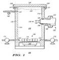
- FIG. 1illustrates a cross-sectional view of a portion of a Chemical-Mechanical Polishing (CMP) system 100 .
- CMP system 100comprises a vessel 110 having a first input port 111 , a second input port 112 , a CMP slurry output port 113 , a CMP slurry sensing port 114 , and a CMP slurry fill level represented by a dashed line 119 .
- CMP slurry output port 113is located below the CMP slurry fill level
- input ports 111 and 112are located below CMP slurry output port 113 .
- CMP slurry sensing port 114is located below output port 113 and the CMP slurry fill level, and CMP slurry sensing port 114 is also located above input ports 111 and 112 .
- the reasons for these preferred relative locations of input ports 111 and 112 , CMP slurry output port 113 , CMP slurry sensing port 114 , and the CMP slurry fill levelare explained hereinafter.
- Vessel 110also comprises an internal wall 115 defining a reservoir 120 .
- wall 115is smooth, but fins (not shown in FIG. 1) may extend from wall 115 to increase the turbulence within reservoir 120 .
- vessel 110 and reservoir 120are preferably sealed tightly so that pumps coupled to input ports 111 , 112 can be used to pump the slurry components into vessel 110 through input ports 111 , 112 and can also be used to pump the slurry out of vessel 110 through output port 113 .
- CMP system 100can include a compliant o-ring 117 , a rigid lid 116 , and mechanical clamps 118 removably coupling or securing lid 116 to the top of vessel 110 .
- O-ring 117is used to provide an air-tight seal.
- CMP system 100can also comprise a dynamic mixing device 130 located at the bottom of vessel 110 .
- Device 130dynamically mixes the CMP slurry within reservoir 120 .
- device 130can include a rotating stirrer or blade 131 that is magnetically coupled to a magnetic actuator 132 .
- blade 131is located within reservoir 120
- magnetic actuator 132is located outside of reservoir 120 .
- a first component of the CMP slurrycan be delivered into the bottom of reservoir 120 through input port 111
- a second component of the CMP slurrycan be delivered into the bottom of reservoir 120 through input port 112 .
- the first componentcan be an oxidizer
- the second componentcan be an abrasive comprised of silica particles in a liquid suspension or a liquid carrier.
- the CMP slurrycan also be comprised of other components such as, for example, a buffered solution.
- device 130dynamically mixes the components together to form the CMP slurry.
- device 130is preferably located adjacent to input ports 111 and 112 such that the components of the CMP slurry can be mixed together immediately after being introduced into reservoir 120 . As the CMP slurry is mixed together, additional amounts of the components of the CMP slurry are introduced into reservoir 120 to increase the amount of CMP slurry in reservoir 120 up to the CMP slurry fill level indicated by dashed line 119 .
- CMP system 100also comprises a pump 171 coupled to input port 111 .
- Pump 171forces the first component of the CMP slurry into reservoir 120 through input port 111 .
- CMP system 100additionally comprises a pump 172 coupled to input port 112 .
- Pump 172forces the second component of the CMP slurry into reservoir 120 through input port 112 .
- Pumps 171 and 172can also be used to force the CMP slurry out of vessel 110 through output port 113 and to deliver the CMP slurry to the semiconductor, dielectric, or metal layer to be planarized or removed.
- CMP system 100further comprises an optical sensor or refractometer 150 located adjacent to CMP slurry sensing port 114 .
- a first portion of refractometer 150is located external to reservoir 120
- a second portion of refractometer 150is located internal to reservoir 120 .
- the second portion of refractometer 150extends through CMP slurry sensing port 114 , from wall 115 into reservoir 120 .
- the second portion of refractometer 150protrudes into reservoir 120 away from or beyond wall 115 .
- the second portion of refractometer 150does not extend into a central portion of reservoir 120 so that interface 152 is not located within a vortex of the CMP slurry, but is located in a relatively high tangential velocity region of the CMP slurry within reservoir 120 .
- CMP slurry sensing port 114 and interface 152are located below the CMP slurry fill level indicated by dashed line 119 to avoid detecting or sensing any vapors within reservoir 120 above the CMP slurry.
- refractometer 150can be a model REFRAC DS Process Refractometer commercially available from the Uniloc Division of Rosemount Analytical, Incorporated of Irvine, Calif.
- This embodiment of refractometer 150comprises a prism 151 , and an interface 152 exists between the CMP slurry and prism 151 .
- prism 151can be comprised of sapphire.
- Refractometer 150is removably coupled or secured to vessel 110 by mechanical clamps 153 , and o-ring 154 is located between the wall of CMP slurry sensing port 114 and refractometer 150 in order to provide an airtight seal between refractometer 150 and port 114 .
- the CMP slurryAs the CMP slurry is introduced into reservoir 120 and is pushed upwards within reservoir 120 towards CMP output port 113 , the CMP slurry moves pass CMP slurry sensing port 114 and refractometer 150 so that refractometer 150 can detect a concentration of the first component in the CMP slurry.
- the first componentis comprised of hydrogen peroxide.
- CMP system 100also comprises a flow rate sensor 160 coupled to CMP slurry output port 113 .
- Sensor 160measures the flow rate of CMP slurry out of reservoir 120 through CMP slurry output port 113 .
- Sensor 160can be a level sensor, but is preferably an instantaneous flow sensor.
- flow rate sensor 160provides a first signal to adjust the flow rate of the first component of the CMP slurry through input port 111 and into vessel 110 .
- Refractometer 150provides a second signal to adjust the flow rate of the first component of the CMP slurry through input port 111 and into vessel 110 .
- CMP system 100also includes other features not illustrated in FIG. 1, but known to those skilled in the art.
- CMP system 100further comprises supply tanks for the first and second components of the CMP slurry.
- the supply tankscan be coupled to pumps 171 and 172 .
- CMP system 100additionally comprises a carrier assembly for supporting a semiconductor substrate that optionally has a plurality of metal and dielectric layers.
- CMP system 100additionally comprises a platen for mechanically polishing the semiconductor substrate or any of its dielectric or metal layers.
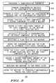
- FIG. 2illustrates a flowchart of a method 200 of manufacturing a semiconductor component.
- Method 200uses CMP system 100 (FIG. 1 ).
- a semiconductor substrateis provided.
- the semiconductor substratecan include at least one semiconductor epitaxial layer overlying a semiconductor support layer.
- a plurality of semiconductor devicesare formed in the semiconductor substrate.
- a first layeris formed over the semiconductor substrate and the semiconductor devices.
- the first layercan be a dielectric layer comprised of silicon dioxide or silicon nitrate.
- the first layeris comprised of a metal such as, for example, copper, aluminum, titanium, or tungsten. When comprised of a metal, the first layer can be used as an interconnect layer.
- first and second components of a mixtureare provided and mixed together.
- the mixtureis a CMP slurry;
- the first componentis an oxidizer such as, for example, hydrogen peroxide;
- the second componentis an abrasive such as, for example, silica particles suspended in a liquid carrier.
- the mixturecan also be comprised of other components known to those skilled in the art of CMP processing.
- the first and second componentsare mixed or combined together within reservoir 120 of FIG. 1 .
- the first and second componentsare dynamically mixed together by, for example, device 130 in FIG. 1 .
- the first and second componentsare mixed together to form a homogenous mixture or solution, which facilitates uniform CMP processing.
- a first additional amount of the first componentcan be added to the mixture at a first injection rate or pump output volumetric rate.
- pump 171 in FIG. 1can operate at a first stroke speed and a first stroke volume to provide the first injection rate. Pump 171 can be used to add the first component into reservoir 120 in FIG. 1 .
- the second componentcan also be added to the mixture.
- pump 172 in FIG. 1can be used to add the second component into reservoir 120 in FIG. 1 .
- a concentration of the first component in the mixtureis optically detected or measured.
- refractometer 150FIG. 1
- step 230is performed in-situ within reservoir 120 (FIG. 1) while dynamically mixing together the first and second components. This fast, automated, and in-situ measurement provides a more accurate measurement of the concentration of the first component than a slow titration process.
- Step 230includes measuring an index of refraction of a portion of the mixture.
- the portion of the mixtureis comprised of a boundary layer in the CMP slurry.
- the boundary layeris a liquid boundary layer comprised of the first component, or the oxidizer, and is devoid of the second component, or the abrasive particles.
- the liquid boundary layeris also comprised of other liquid components of the CMP slurry such as, for example, the liquid carrier for the abrasive particles.
- the liquid boundary layeris located around each of the abrasive particles.
- the refractometershines a light through a solid material such as, for example, prism 151 (FIG.
- the refractometeroptically detects the angle of the light reflected off of interface 152 to determine the index of refraction of the liquid boundary layer surrounding the CMP slurry abrasive particles.
- the refractometercan be configured to detect a specific range of index of refraction. As an example, the range of the index of refraction can be approximately 1.333 to 1.340 when prism 151 is comprised of sapphire and when the first component is comprised of hydrogen peroxide.
- the measured index of refractionis directly and linearly proportional to the concentration of the first component within the mixture.
- This index of refraction measurementis not affected by the color, turgidity, clouding, solids, concentration of solids, or flow rate of the mixture.
- the concentration determined in step 230is subsequently used to determine a second injection rate for the first component of the mixture.
- a flow rate of the mixtureis detected or measured.
- flow rate sensor 160 in FIG. 1can be used to perform step 235 in FIG. 2 .
- the flow rate determined in step 235is subsequently used to determine a second injection rate for the first component of the mixture.
- the sequence of steps 230 and 235can be reversed.
- the concentration determined in step 230 and the flow rate determined in step 235are used to determine fuzzy logic parameters or variables.
- the index of refraction measured in step 230can be converted into a first signal by refractometer 150 (FIG. 1 ).
- the first signalcan be a current or a voltage.
- This first signalis subsequently converted into at least one, and possibly two, fuzzy logic parameters or variables.
- the flow rate determined in step 235is converted into a second signal by flow rate sensor 160 (FIG. 1 ).
- this second signalcan be a current or a voltage.
- This second signalis subsequently converted into at least one, and possibly two, additional fuzzy logic parameters or variables. The details of these conversions into fuzzy logic variables are described in more detail with respect to FIGS. 3 and 4.
- step 245 of method 200the fuzzy logic variables are used to determine a second injection rate or pump stroke rate for the first component of the mixture.
- the details of step 245are explained in more detail hereinafter with reference to FIGS. 5 and 6.
- steps 230 , 235 , 240 , and 245can be performed within 30 seconds.
- a second additional amount of the first componentis added to the mixture at the second injection rate.
- the second injection ratewill most likely be different from the first injection rate.
- pump 171 in FIG. 1can operate at a second speed to provide the second injection rate. Pump 171 can be used to add the first component into reservoir 120 in FIG. 1 .
- the second componentcan also be added to the mixture.
- pump 172 in FIG. 1can be used to add the second component into reservoir 120 in FIG. 1 .
- the mixtureis applied to the first layer over the semiconductor substrate, and at a step 260 of method 200 , the mixture is used to chemically-mechanically polished to planarized or remove the first layer.
- FIG. 3illustrates a fuzzy logic graph used in method 200 of FIG. 2 .
- This graph in FIG. 3converts the first signal from the refractometer into at least one fuzzy logic variable.
- the first signalis a current in FIG. 3 .
- the x-axis or horizontal axis of the graphrepresents the output current from the refractometer. This x-axis ranges from approximately 4 milliAmperes (mA) to 20 mA.
- the y-axis or vertical axisrepresents the fuzzy grade of the fuzzy logic variable. The y-axis ranges from 0 to 1.
- the NS and PS fuzzy logic variablescan represent control limits while the NM and PM fuzzy logic variables can represent specification limits.
- the refractometermay convert the index of refraction into a current having a magnitude of approximately 11 mA, and the graph in FIG. 3 is used to convert the 11 mA output into two different fuzzy logic variables.
- the first fuzzy logic variableis NS with a fuzzy grade of approximately 0.8
- the second fuzzy logic variableis NM with a fuzzy grade of approximately 0.2.
- FIG. 4illustrates a fuzzy logic graph used in method 200 of FIG. 2 .
- This graph in FIG. 4converts the second signal from the flow rate sensor into at least one fuzzy logic variable.
- the second signalis a current in FIG. 4 .
- the x-axis or horizontal axis of the graphrepresents the output current from the flow rate sensor.
- the x-axisranges from approximately 4 mA to 20 mA.
- the y-axis or vertical axisrepresents the fuzzy grade of the fuzzy logic variable.
- the y-axisranges from 0 to 1.
- the fuzzy logic graph of FIG. 4also includes seven fuzzy logic variables: NL, NM, NS, ZR, PS, PM, and PL.
- the NS and PS fuzzy logic variablescan represent control limits while the NM and PM fuzzy logic variable can represent specification limits.
- the flow rate sensorcan convert the flow rate into a current having a magnitude of approximately 16 mA, and the graph in FIG. 4 is used to convert the 16 mA output into two fuzzy logic variables.
- the first fuzzy logic variableis PS with a fuzzy grade of approximately 0.6
- the second fuzzy variable logicis PM with a fuzzy grade of approximately 0.4.
- FIG. 5illustrates a fuzzy logic table used in method 200 of FIG. 2 .
- the table of FIG. 5converts the fuzzy logic variables from FIGS. 3 and 4 into other fuzzy logic variables.
- the table in FIG. 5includes seven columns representing the seven fuzzy logic variables in FIG. 3, and the table in FIG. 5 also has seven rows representing the seven fuzzy logic variables of FIG. 4 .
- the two fuzzy logic variables determined in FIG. 3were NS and NM, and the two fuzzy logic variables determined in FIG. 4 were PS and PM.
- the intersection of these four fuzzy logic variables in the table of FIG. 5produces four other fuzzy logic variables. For example, the intersection of the NM column with the PM row produces a fuzzy logic variable of PM, and the intersection of the NM column with PS row produces a fuzzy logic variable PM.
- the intersection of the NS column with the PM rowproduces a fuzzy logic variable PM
- the intersection of the NS column with the PS rowproduces a fuzzy logic variable PS.
- the four resulting fuzzy logic variablesare PM, PM, PM, and PS. These four fuzzy variables are averaged to produce a composite fuzzy logic variable of approximately 75 percent PM and 25 percent PS.
- FIG. 6illustrates another fuzzy logic graph used in method 200 of FIG. 2 .
- the graph in FIG. 6converts the composite fuzzy logic variable of FIG. 5 into the second injection rate for the first component of the mixture.
- the x-axis or horizontal axis of the graph in FIG. 6represents the input current for the pump that controls the second injection rate.
- the x-axisranges from approximately 4 mA to 20 mA.
- the y-axis or vertical axisrepresents the fuzzy grade of the composite fuzzy logic variable.
- the y-axisranges from 0 to 1.
- the graph in FIG. 6includes seven fuzzy logic variables: NL, NM, NS, ZR, PS, PM, and PL. Continuing with the example from FIG.
- the composite fuzzy logic variable of 75 percent PM and 25 percent PSproduces a current of approximately 15.5 mA in FIG. 6 .
- This currentis supplied to the pump for the first component.
- the 15.5 mAcan be supplied to pump 171 in FIG. 1 to establish the second injection rate for the first component of the mixture.
- the thirty second optical detection cycleis much faster and more accurate than the fifteen minute titration cycle of the prior art.
- the optical detectionis in-line and non-intrusive. Off-line sampling is not required, and no reagents are required. Accordingly, minimal training is required to use the CPM system or method described herein.
- the optical systemis estimated to be approximately $30,000.00 to $70,000.00 less expensive than a conventional titration system. Thus, the method and system are also cost effective.
- the fuzzy logic control systemprovides a faster and more accurate response that will not overshoot the intended target and that will also not oscillate around the intended target.
- the method described hereinis not limited to CMP processes, but can also be used for other processes such as, for example, semiconductor wafer cleaning where the index of refraction of the solute is different than that of the solvent and provides a significant change in the index of refraction depending on its concentration in the solvent. Accordingly, the disclosure of embodiments of the invention is intended to be illustrative of the scope of the invention and is not intended to be limiting. It is intended that the scope of the invention shall be limited only to the extent required by the appended claims.
Landscapes
- Engineering & Computer Science (AREA)
- Mechanical Engineering (AREA)
- Chemical & Material Sciences (AREA)
- Chemical Kinetics & Catalysis (AREA)
- Physics & Mathematics (AREA)
- Condensed Matter Physics & Semiconductors (AREA)
- General Physics & Mathematics (AREA)
- Manufacturing & Machinery (AREA)
- Computer Hardware Design (AREA)
- Microelectronics & Electronic Packaging (AREA)
- Power Engineering (AREA)
- Mechanical Treatment Of Semiconductor (AREA)
- Finish Polishing, Edge Sharpening, And Grinding By Specific Grinding Devices (AREA)
- Grinding-Machine Dressing And Accessory Apparatuses (AREA)
Abstract
Description
Claims (6)
Priority Applications (8)
| Application Number | Priority Date | Filing Date | Title |
|---|---|---|---|
| US09/574,969US6267641B1 (en) | 2000-05-19 | 2000-05-19 | Method of manufacturing a semiconductor component and chemical-mechanical polishing system therefor |
| PCT/US2001/011143WO2001089767A2 (en) | 2000-05-19 | 2001-04-06 | A chemical-mechanical polishing system for the manufacture of semiconductor devices |
| JP2001585993AJP4869536B2 (en) | 2000-05-19 | 2001-04-06 | Chemical mechanical polishing system for semiconductor manufacturing |
| CNB018114202ACN100402236C (en) | 2000-05-19 | 2001-04-06 | Method for manufacturing semiconductor element and chemical mechanical polishing system thereof |
| AU2001253180AAU2001253180A1 (en) | 2000-05-19 | 2001-04-06 | A chemical-mechanical polishing system for the manufacture of semiconductor devices |
| KR1020027015502AKR100777147B1 (en) | 2000-05-19 | 2001-04-06 | Chemical mechanical polishing systems for semiconductor device manufacturing |
| EP01926659AEP1286808A2 (en) | 2000-05-19 | 2001-04-06 | A chemical-mechanical polishing system for the manufacture of semiconductor devices |
| TW090110067ATW504764B (en) | 2000-05-19 | 2001-04-27 | Method of manufacturing a semiconductor component |
Applications Claiming Priority (1)
| Application Number | Priority Date | Filing Date | Title |
|---|---|---|---|
| US09/574,969US6267641B1 (en) | 2000-05-19 | 2000-05-19 | Method of manufacturing a semiconductor component and chemical-mechanical polishing system therefor |
Publications (1)
| Publication Number | Publication Date |
|---|---|
| US6267641B1true US6267641B1 (en) | 2001-07-31 |
Family
ID=24298369
Family Applications (1)
| Application Number | Title | Priority Date | Filing Date |
|---|---|---|---|
| US09/574,969Expired - LifetimeUS6267641B1 (en) | 2000-05-19 | 2000-05-19 | Method of manufacturing a semiconductor component and chemical-mechanical polishing system therefor |
Country Status (8)
| Country | Link |
|---|---|
| US (1) | US6267641B1 (en) |
| EP (1) | EP1286808A2 (en) |
| JP (1) | JP4869536B2 (en) |
| KR (1) | KR100777147B1 (en) |
| CN (1) | CN100402236C (en) |
| AU (1) | AU2001253180A1 (en) |
| TW (1) | TW504764B (en) |
| WO (1) | WO2001089767A2 (en) |
Cited By (24)
| Publication number | Priority date | Publication date | Assignee | Title |
|---|---|---|---|---|
| US20020048213A1 (en)* | 2000-07-31 | 2002-04-25 | Wilmer Jeffrey Alexander | Method and apparatus for blending process materials |
| US6464562B1 (en)* | 2001-12-19 | 2002-10-15 | Winbond Electronics Corporation | System and method for in-situ monitoring slurry flow rate during a chemical mechanical polishing process |
| US20020171837A1 (en)* | 2001-05-17 | 2002-11-21 | Chi-Feng Cheng | System for monitoring oxidant concentration of slurry in a chemical mechanical polishing process |
| US6709311B2 (en) | 2001-08-13 | 2004-03-23 | Particle Measuring Systems, Inc. | Spectroscopic measurement of the chemical constituents of a CMP slurry |
| US20040057334A1 (en)* | 2001-07-31 | 2004-03-25 | Wilmer Jeffrey Alexander | Method and apparatus for blending process materials |
| US20040100860A1 (en)* | 2002-07-19 | 2004-05-27 | Wilmer Jeffrey A. | Method and apparatus for blending process materials |
| US20040166584A1 (en)* | 2000-12-21 | 2004-08-26 | Ashutosh Misra | Method and apparatus for monitoring of a chemical characteristic of a process chemical |
| US20040206374A1 (en)* | 2001-10-09 | 2004-10-21 | Dinesh Chopra | Inline monitoring of pad loading for CuCMP and developing an endpoint technique for cleaning |
| US7066191B2 (en) | 2002-04-12 | 2006-06-27 | Kinetics Germany Gmbh | Installation for making available highly pure fine chemicals |
| US20060158653A1 (en)* | 2005-01-14 | 2006-07-20 | Jetalon Solutions, Inc. | Metal ion concentration analysis for liquids |
| US20070070332A1 (en)* | 2005-09-26 | 2007-03-29 | Jetalon Solutions, Inc. | Method for a liquid chemical concentration analysis system |
| US20100296079A1 (en)* | 2009-05-20 | 2010-11-25 | Jetalon Solutions, Inc. | Sensing system and method |
| US11446788B2 (en) | 2014-10-17 | 2022-09-20 | Applied Materials, Inc. | Precursor formulations for polishing pads produced by an additive manufacturing process |
| US11471999B2 (en) | 2017-07-26 | 2022-10-18 | Applied Materials, Inc. | Integrated abrasive polishing pads and manufacturing methods |
| US11524384B2 (en) | 2017-08-07 | 2022-12-13 | Applied Materials, Inc. | Abrasive delivery polishing pads and manufacturing methods thereof |
| US11685014B2 (en) | 2018-09-04 | 2023-06-27 | Applied Materials, Inc. | Formulations for advanced polishing pads |
| US11724362B2 (en) | 2014-10-17 | 2023-08-15 | Applied Materials, Inc. | Polishing pads produced by an additive manufacturing process |
| US11745302B2 (en) | 2014-10-17 | 2023-09-05 | Applied Materials, Inc. | Methods and precursor formulations for forming advanced polishing pads by use of an additive manufacturing process |
| US11772229B2 (en) | 2016-01-19 | 2023-10-03 | Applied Materials, Inc. | Method and apparatus for forming porous advanced polishing pads using an additive manufacturing process |
| US11878389B2 (en) | 2021-02-10 | 2024-01-23 | Applied Materials, Inc. | Structures formed using an additive manufacturing process for regenerating surface texture in situ |
| US11958162B2 (en) | 2014-10-17 | 2024-04-16 | Applied Materials, Inc. | CMP pad construction with composite material properties using additive manufacturing processes |
| US11964359B2 (en) | 2015-10-30 | 2024-04-23 | Applied Materials, Inc. | Apparatus and method of forming a polishing article that has a desired zeta potential |
| US11986922B2 (en) | 2015-11-06 | 2024-05-21 | Applied Materials, Inc. | Techniques for combining CMP process tracking data with 3D printed CMP consumables |
| US12023853B2 (en) | 2014-10-17 | 2024-07-02 | Applied Materials, Inc. | Polishing articles and integrated system and methods for manufacturing chemical mechanical polishing articles |
Families Citing this family (3)
| Publication number | Priority date | Publication date | Assignee | Title |
|---|---|---|---|---|
| CN106442408A (en)* | 2016-10-12 | 2017-02-22 | 上海胤飞自动化科技有限公司 | Chemical-mechanical polishing liquid automatic preparation control system |
| CN114193328A (en)* | 2020-09-18 | 2022-03-18 | 中国科学院微电子研究所 | Polishing agent container and polishing agent supply method |
| CN116117687A (en)* | 2021-11-15 | 2023-05-16 | 成都高真科技有限公司 | Abrasive supply unit for CMP process |
Citations (12)
| Publication number | Priority date | Publication date | Assignee | Title |
|---|---|---|---|---|
| US5597595A (en) | 1995-04-07 | 1997-01-28 | Abbott Laboratories | Low pH beverage fortified with calcium and vitamin D |
| US5750440A (en) | 1995-11-20 | 1998-05-12 | Motorola, Inc. | Apparatus and method for dynamically mixing slurry for chemical mechanical polishing |
| US5755614A (en) | 1996-07-29 | 1998-05-26 | Integrated Process Equipment Corporation | Rinse water recycling in CMP apparatus |
| US5846398A (en)* | 1996-08-23 | 1998-12-08 | Sematech, Inc. | CMP slurry measurement and control technique |
| US5905571A (en) | 1995-08-30 | 1999-05-18 | Sandia Corporation | Optical apparatus for forming correlation spectrometers and optical processors |
| US5911619A (en) | 1997-03-26 | 1999-06-15 | International Business Machines Corporation | Apparatus for electrochemical mechanical planarization |
| US5914275A (en) | 1992-05-26 | 1999-06-22 | Kabushiki Kaisha Toshiba | Polishing apparatus and method for planarizing layer on a semiconductor wafer |
| US5922606A (en) | 1997-09-16 | 1999-07-13 | Nalco Chemical Company | Fluorometric method for increasing the efficiency of the rinsing and water recovery process in the manufacture of semiconductor chips |
| US5939831A (en) | 1996-11-13 | 1999-08-17 | Applied Materials, Inc. | Methods and apparatus for pre-stabilized plasma generation for microwave clean applications |
| US6106728A (en)* | 1997-06-23 | 2000-08-22 | Iida; Shinya | Slurry recycling system and method for CMP apparatus |
| US6126531A (en)* | 1998-03-30 | 2000-10-03 | Speedfam Co., Ltd. | Slurry recycling system of CMP apparatus and method of same |
| US6183352B1 (en)* | 1998-08-28 | 2001-02-06 | Nec Corporation | Slurry recycling apparatus and slurry recycling method for chemical-mechanical polishing technique |
Family Cites Families (6)
| Publication number | Priority date | Publication date | Assignee | Title |
|---|---|---|---|---|
| JPH05269462A (en)* | 1992-03-26 | 1993-10-19 | Showa Alum Corp | Grinding effluent recovery method |
| JP2971714B2 (en)* | 1993-10-01 | 1999-11-08 | 住友金属工業株式会社 | Mirror polishing method for semiconductor substrate |
| JPH10223599A (en) | 1998-03-12 | 1998-08-21 | Dainippon Screen Mfg Co Ltd | Immersion substrate-treating device |
| JP2000117635A (en)* | 1998-10-15 | 2000-04-25 | Sumitomo Metal Ind Ltd | Polishing method and polishing system |
| JP2000260736A (en)* | 1999-03-04 | 2000-09-22 | Rohm Co Ltd | Manufacture of electronic device and chemical mechanical polishing device |
| US6048256A (en)* | 1999-04-06 | 2000-04-11 | Lucent Technologies Inc. | Apparatus and method for continuous delivery and conditioning of a polishing slurry |
- 2000
- 2000-05-19USUS09/574,969patent/US6267641B1/ennot_activeExpired - Lifetime
- 2001
- 2001-04-06JPJP2001585993Apatent/JP4869536B2/ennot_activeExpired - Fee Related
- 2001-04-06AUAU2001253180Apatent/AU2001253180A1/ennot_activeAbandoned
- 2001-04-06EPEP01926659Apatent/EP1286808A2/ennot_activeWithdrawn
- 2001-04-06WOPCT/US2001/011143patent/WO2001089767A2/enactiveApplication Filing
- 2001-04-06CNCNB018114202Apatent/CN100402236C/ennot_activeExpired - Fee Related
- 2001-04-06KRKR1020027015502Apatent/KR100777147B1/ennot_activeExpired - Fee Related
- 2001-04-27TWTW090110067Apatent/TW504764B/ennot_activeIP Right Cessation
Patent Citations (12)
| Publication number | Priority date | Publication date | Assignee | Title |
|---|---|---|---|---|
| US5914275A (en) | 1992-05-26 | 1999-06-22 | Kabushiki Kaisha Toshiba | Polishing apparatus and method for planarizing layer on a semiconductor wafer |
| US5597595A (en) | 1995-04-07 | 1997-01-28 | Abbott Laboratories | Low pH beverage fortified with calcium and vitamin D |
| US5905571A (en) | 1995-08-30 | 1999-05-18 | Sandia Corporation | Optical apparatus for forming correlation spectrometers and optical processors |
| US5750440A (en) | 1995-11-20 | 1998-05-12 | Motorola, Inc. | Apparatus and method for dynamically mixing slurry for chemical mechanical polishing |
| US5755614A (en) | 1996-07-29 | 1998-05-26 | Integrated Process Equipment Corporation | Rinse water recycling in CMP apparatus |
| US5846398A (en)* | 1996-08-23 | 1998-12-08 | Sematech, Inc. | CMP slurry measurement and control technique |
| US5939831A (en) | 1996-11-13 | 1999-08-17 | Applied Materials, Inc. | Methods and apparatus for pre-stabilized plasma generation for microwave clean applications |
| US5911619A (en) | 1997-03-26 | 1999-06-15 | International Business Machines Corporation | Apparatus for electrochemical mechanical planarization |
| US6106728A (en)* | 1997-06-23 | 2000-08-22 | Iida; Shinya | Slurry recycling system and method for CMP apparatus |
| US5922606A (en) | 1997-09-16 | 1999-07-13 | Nalco Chemical Company | Fluorometric method for increasing the efficiency of the rinsing and water recovery process in the manufacture of semiconductor chips |
| US6126531A (en)* | 1998-03-30 | 2000-10-03 | Speedfam Co., Ltd. | Slurry recycling system of CMP apparatus and method of same |
| US6183352B1 (en)* | 1998-08-28 | 2001-02-06 | Nec Corporation | Slurry recycling apparatus and slurry recycling method for chemical-mechanical polishing technique |
Non-Patent Citations (3)
| Title |
|---|
| Omron, "Fuzzy Guide Book", 1992, whole book. |
| Rosemount Analytical, "Process Refractometer" Instruction Manual-P/N 510REFRACDS, May 1998, Chapters 1.0-1.3. |
| Rosemount Analytical, "Process Refractometer" Product Data Sheet-PDS 71-REFRACDS, Feb. 1998, pp. 1-3. |
Cited By (41)
| Publication number | Priority date | Publication date | Assignee | Title |
|---|---|---|---|---|
| US20080062813A1 (en)* | 2000-07-31 | 2008-03-13 | Celerity, Inc. | Method and apparatus for blending process materials |
| US20020048213A1 (en)* | 2000-07-31 | 2002-04-25 | Wilmer Jeffrey Alexander | Method and apparatus for blending process materials |
| US20110153084A1 (en)* | 2000-07-31 | 2011-06-23 | Mega Fluid Systems, Inc. | Method and Apparatus for Blending Process Materials |
| US6923568B2 (en) | 2000-07-31 | 2005-08-02 | Celerity, Inc. | Method and apparatus for blending process materials |
| US20040166584A1 (en)* | 2000-12-21 | 2004-08-26 | Ashutosh Misra | Method and apparatus for monitoring of a chemical characteristic of a process chemical |
| US6856394B2 (en)* | 2001-05-17 | 2005-02-15 | Macronix International Co., Ltd. | System for monitoring oxidant concentration of slurry in a chemical mechanical polishing process |
| US20020171837A1 (en)* | 2001-05-17 | 2002-11-21 | Chi-Feng Cheng | System for monitoring oxidant concentration of slurry in a chemical mechanical polishing process |
| US20040057334A1 (en)* | 2001-07-31 | 2004-03-25 | Wilmer Jeffrey Alexander | Method and apparatus for blending process materials |
| US7905653B2 (en) | 2001-07-31 | 2011-03-15 | Mega Fluid Systems, Inc. | Method and apparatus for blending process materials |
| US6709311B2 (en) | 2001-08-13 | 2004-03-23 | Particle Measuring Systems, Inc. | Spectroscopic measurement of the chemical constituents of a CMP slurry |
| US8557132B2 (en)* | 2001-10-09 | 2013-10-15 | Micron Technology, Inc. | Inline monitoring of pad loading for CuCMP and developing an endpoint technique for cleaning |
| US20040206374A1 (en)* | 2001-10-09 | 2004-10-21 | Dinesh Chopra | Inline monitoring of pad loading for CuCMP and developing an endpoint technique for cleaning |
| US6464562B1 (en)* | 2001-12-19 | 2002-10-15 | Winbond Electronics Corporation | System and method for in-situ monitoring slurry flow rate during a chemical mechanical polishing process |
| US7066191B2 (en) | 2002-04-12 | 2006-06-27 | Kinetics Germany Gmbh | Installation for making available highly pure fine chemicals |
| US7344298B2 (en) | 2002-07-19 | 2008-03-18 | Celerity, Inc. | Method and apparatus for blending process materials |
| US20040100860A1 (en)* | 2002-07-19 | 2004-05-27 | Wilmer Jeffrey A. | Method and apparatus for blending process materials |
| US7317533B2 (en) | 2005-01-14 | 2008-01-08 | Jetalon Solutions, Inc. | Metal ion concentration analysis for liquids |
| US20060158653A1 (en)* | 2005-01-14 | 2006-07-20 | Jetalon Solutions, Inc. | Metal ion concentration analysis for liquids |
| US20080001105A1 (en)* | 2005-09-26 | 2008-01-03 | Jetalon Solutions, Inc. | Method for a liquid chemical concentration analysis system |
| US7319523B2 (en) | 2005-09-26 | 2008-01-15 | Jetalon Solutions, Inc. | Apparatus for a liquid chemical concentration analysis system |
| US20070070331A1 (en)* | 2005-09-26 | 2007-03-29 | Jetalon Solutions, Inc. | Method and apparatus for a liquid chemical concentration analysis system |
| US20070070330A1 (en)* | 2005-09-26 | 2007-03-29 | Jetalon Solutions, Inc. | Method and apparatus for a liquid chemical concentration analysis system |
| US7397547B2 (en) | 2005-09-26 | 2008-07-08 | Jetalon Solutions, Inc. | Method and apparatus for a liquid chemical concentration analysis system |
| US7471379B2 (en) | 2005-09-26 | 2008-12-30 | Jetalon Solutions, Inc. | Method for a liquid chemical concentration analysis system |
| US7268864B2 (en) | 2005-09-26 | 2007-09-11 | Jetalon Solutions, Inc. | Method for a liquid chemical concentration analysis system |
| US20070070332A1 (en)* | 2005-09-26 | 2007-03-29 | Jetalon Solutions, Inc. | Method for a liquid chemical concentration analysis system |
| US8602640B2 (en) | 2009-05-20 | 2013-12-10 | Entegris—Jetalon Solutions, Inc. | Sensing system and method |
| US20100296079A1 (en)* | 2009-05-20 | 2010-11-25 | Jetalon Solutions, Inc. | Sensing system and method |
| US11958162B2 (en) | 2014-10-17 | 2024-04-16 | Applied Materials, Inc. | CMP pad construction with composite material properties using additive manufacturing processes |
| US11724362B2 (en) | 2014-10-17 | 2023-08-15 | Applied Materials, Inc. | Polishing pads produced by an additive manufacturing process |
| US11745302B2 (en) | 2014-10-17 | 2023-09-05 | Applied Materials, Inc. | Methods and precursor formulations for forming advanced polishing pads by use of an additive manufacturing process |
| US11446788B2 (en) | 2014-10-17 | 2022-09-20 | Applied Materials, Inc. | Precursor formulations for polishing pads produced by an additive manufacturing process |
| US12023853B2 (en) | 2014-10-17 | 2024-07-02 | Applied Materials, Inc. | Polishing articles and integrated system and methods for manufacturing chemical mechanical polishing articles |
| US11964359B2 (en) | 2015-10-30 | 2024-04-23 | Applied Materials, Inc. | Apparatus and method of forming a polishing article that has a desired zeta potential |
| US11986922B2 (en) | 2015-11-06 | 2024-05-21 | Applied Materials, Inc. | Techniques for combining CMP process tracking data with 3D printed CMP consumables |
| US11772229B2 (en) | 2016-01-19 | 2023-10-03 | Applied Materials, Inc. | Method and apparatus for forming porous advanced polishing pads using an additive manufacturing process |
| US11471999B2 (en) | 2017-07-26 | 2022-10-18 | Applied Materials, Inc. | Integrated abrasive polishing pads and manufacturing methods |
| US11980992B2 (en) | 2017-07-26 | 2024-05-14 | Applied Materials, Inc. | Integrated abrasive polishing pads and manufacturing methods |
| US11524384B2 (en) | 2017-08-07 | 2022-12-13 | Applied Materials, Inc. | Abrasive delivery polishing pads and manufacturing methods thereof |
| US11685014B2 (en) | 2018-09-04 | 2023-06-27 | Applied Materials, Inc. | Formulations for advanced polishing pads |
| US11878389B2 (en) | 2021-02-10 | 2024-01-23 | Applied Materials, Inc. | Structures formed using an additive manufacturing process for regenerating surface texture in situ |
Also Published As
| Publication number | Publication date |
|---|---|
| KR20020097287A (en) | 2002-12-31 |
| JP2004515905A (en) | 2004-05-27 |
| EP1286808A2 (en) | 2003-03-05 |
| WO2001089767A2 (en) | 2001-11-29 |
| AU2001253180A1 (en) | 2001-12-03 |
| JP4869536B2 (en) | 2012-02-08 |
| KR100777147B1 (en) | 2007-11-19 |
| TW504764B (en) | 2002-10-01 |
| WO2001089767A3 (en) | 2002-07-25 |
| CN100402236C (en) | 2008-07-16 |
| CN1438932A (en) | 2003-08-27 |
Similar Documents
| Publication | Publication Date | Title |
|---|---|---|
| US6267641B1 (en) | Method of manufacturing a semiconductor component and chemical-mechanical polishing system therefor | |
| CN1332741C (en) | Method and apparatus for blending process materials | |
| Pate et al. | Chemical metrology methods for CMP quality | |
| KR100548750B1 (en) | Conductivity feedback control system for slurry mixing | |
| US9852915B2 (en) | Etching apparatus | |
| Andreasen et al. | Integrating electrochemical detection with centrifugal microfluidics for real-time and fully automated sample testing | |
| KR19980081288A (en) | Ultra-pure chemical dilution system used in microelectronics industry | |
| US6039055A (en) | Wafer cleaning with dissolved gas concentration control | |
| US20240059549A1 (en) | Liquid supply system and liquid preparation method | |
| US6955764B2 (en) | Method and apparatus for preparing slurry for CMP apparatus | |
| Laurell et al. | A micromachined enzyme reactor in⪢ 110>-oriented silicon | |
| EP1068373A1 (en) | Automated chemical process control system | |
| WO1996030934A1 (en) | Carrier matrix for integrated microanalysis systems, method for the production thereof and use of the same | |
| US20030132417A1 (en) | Method and apparatus for preparing slurry for CMP apparatus | |
| JP2000230894A (en) | Specific gravity measuring device | |
| Cho | Batch-dissolved wafer process for low-cost sensor applications | |
| US20020094579A1 (en) | Methods of determining concentration of a component of a slurry | |
| JP2002267511A (en) | Flow measuring instrument and substrate treating device using the same | |
| Hinze et al. | Point of Use Quality Control of CMP Slurries | |
| JPH01282450A (en) | Analysis container | |
| Singh et al. | A symposium | |
| SU1651194A1 (en) | Method of determination of size distribution of dispersed phase of a suspension | |
| JPH0145580B2 (en) | ||
| KR970063435A (en) | Semiconductor manufacturing equipment | |
| KR20010095894A (en) | Method for measuring End Point of Chemical Mechanical Polishing |
Legal Events
| Date | Code | Title | Description |
|---|---|---|---|
| AS | Assignment | Owner name:MOTOROLA, INC., ILLINOIS Free format text:ASSIGNMENT OF ASSIGNORS INTEREST;ASSIGNORS:VANELL, JAMES F.;BRAY, CHAD B.;REEL/FRAME:011209/0250 Effective date:20000518 | |
| STCF | Information on status: patent grant | Free format text:PATENTED CASE | |
| CC | Certificate of correction | ||
| AS | Assignment | Owner name:FREESCALE SEMICONDUCTOR, INC., TEXAS Free format text:ASSIGNMENT OF ASSIGNORS INTEREST;ASSIGNOR:MOTOROLA, INC.;REEL/FRAME:015698/0657 Effective date:20040404 Owner name:FREESCALE SEMICONDUCTOR, INC.,TEXAS Free format text:ASSIGNMENT OF ASSIGNORS INTEREST;ASSIGNOR:MOTOROLA, INC.;REEL/FRAME:015698/0657 Effective date:20040404 | |
| FPAY | Fee payment | Year of fee payment:4 | |
| AS | Assignment | Owner name:CITIBANK, N.A. AS COLLATERAL AGENT, NEW YORK Free format text:SECURITY AGREEMENT;ASSIGNORS:FREESCALE SEMICONDUCTOR, INC.;FREESCALE ACQUISITION CORPORATION;FREESCALE ACQUISITION HOLDINGS CORP.;AND OTHERS;REEL/FRAME:018855/0129 Effective date:20061201 Owner name:CITIBANK, N.A. AS COLLATERAL AGENT,NEW YORK Free format text:SECURITY AGREEMENT;ASSIGNORS:FREESCALE SEMICONDUCTOR, INC.;FREESCALE ACQUISITION CORPORATION;FREESCALE ACQUISITION HOLDINGS CORP.;AND OTHERS;REEL/FRAME:018855/0129 Effective date:20061201 | |
| FPAY | Fee payment | Year of fee payment:8 | |
| AS | Assignment | Owner name:CITIBANK, N.A., AS COLLATERAL AGENT,NEW YORK Free format text:SECURITY AGREEMENT;ASSIGNOR:FREESCALE SEMICONDUCTOR, INC.;REEL/FRAME:024397/0001 Effective date:20100413 Owner name:CITIBANK, N.A., AS COLLATERAL AGENT, NEW YORK Free format text:SECURITY AGREEMENT;ASSIGNOR:FREESCALE SEMICONDUCTOR, INC.;REEL/FRAME:024397/0001 Effective date:20100413 | |
| FPAY | Fee payment | Year of fee payment:12 | |
| AS | Assignment | Owner name:CITIBANK, N.A., AS NOTES COLLATERAL AGENT, NEW YORK Free format text:SECURITY AGREEMENT;ASSIGNOR:FREESCALE SEMICONDUCTOR, INC.;REEL/FRAME:030633/0424 Effective date:20130521 Owner name:CITIBANK, N.A., AS NOTES COLLATERAL AGENT, NEW YOR Free format text:SECURITY AGREEMENT;ASSIGNOR:FREESCALE SEMICONDUCTOR, INC.;REEL/FRAME:030633/0424 Effective date:20130521 | |
| AS | Assignment | Owner name:CITIBANK, N.A., AS NOTES COLLATERAL AGENT, NEW YORK Free format text:SECURITY AGREEMENT;ASSIGNOR:FREESCALE SEMICONDUCTOR, INC.;REEL/FRAME:031591/0266 Effective date:20131101 Owner name:CITIBANK, N.A., AS NOTES COLLATERAL AGENT, NEW YOR Free format text:SECURITY AGREEMENT;ASSIGNOR:FREESCALE SEMICONDUCTOR, INC.;REEL/FRAME:031591/0266 Effective date:20131101 | |
| AS | Assignment | Owner name:FREESCALE SEMICONDUCTOR, INC., TEXAS Free format text:PATENT RELEASE;ASSIGNOR:CITIBANK, N.A., AS COLLATERAL AGENT;REEL/FRAME:037356/0553 Effective date:20151207 Owner name:FREESCALE SEMICONDUCTOR, INC., TEXAS Free format text:PATENT RELEASE;ASSIGNOR:CITIBANK, N.A., AS COLLATERAL AGENT;REEL/FRAME:037354/0225 Effective date:20151207 Owner name:FREESCALE SEMICONDUCTOR, INC., TEXAS Free format text:PATENT RELEASE;ASSIGNOR:CITIBANK, N.A., AS COLLATERAL AGENT;REEL/FRAME:037356/0143 Effective date:20151207 | |
| AS | Assignment | Owner name:MORGAN STANLEY SENIOR FUNDING, INC., MARYLAND Free format text:ASSIGNMENT AND ASSUMPTION OF SECURITY INTEREST IN PATENTS;ASSIGNOR:CITIBANK, N.A.;REEL/FRAME:037486/0517 Effective date:20151207 | |
| AS | Assignment | Owner name:MORGAN STANLEY SENIOR FUNDING, INC., MARYLAND Free format text:ASSIGNMENT AND ASSUMPTION OF SECURITY INTEREST IN PATENTS;ASSIGNOR:CITIBANK, N.A.;REEL/FRAME:037518/0292 Effective date:20151207 | |
| AS | Assignment | Owner name:NORTH STAR INNOVATIONS INC., CALIFORNIA Free format text:ASSIGNMENT OF ASSIGNORS INTEREST;ASSIGNOR:FREESCALE SEMICONDUCTOR, INC.;REEL/FRAME:037694/0264 Effective date:20151002 | |
| AS | Assignment | Owner name:NXP, B.V., F/K/A FREESCALE SEMICONDUCTOR, INC., NETHERLANDS Free format text:RELEASE BY SECURED PARTY;ASSIGNOR:MORGAN STANLEY SENIOR FUNDING, INC.;REEL/FRAME:040925/0001 Effective date:20160912 Owner name:NXP, B.V., F/K/A FREESCALE SEMICONDUCTOR, INC., NE Free format text:RELEASE BY SECURED PARTY;ASSIGNOR:MORGAN STANLEY SENIOR FUNDING, INC.;REEL/FRAME:040925/0001 Effective date:20160912 | |
| AS | Assignment | Owner name:NXP B.V., NETHERLANDS Free format text:RELEASE BY SECURED PARTY;ASSIGNOR:MORGAN STANLEY SENIOR FUNDING, INC.;REEL/FRAME:040928/0001 Effective date:20160622 | |
| AS | Assignment | Owner name:MORGAN STANLEY SENIOR FUNDING, INC., MARYLAND Free format text:CORRECTIVE ASSIGNMENT TO CORRECT THE REMOVE PATENTS 8108266 AND 8062324 AND REPLACE THEM WITH 6108266 AND 8060324 PREVIOUSLY RECORDED ON REEL 037518 FRAME 0292. ASSIGNOR(S) HEREBY CONFIRMS THE ASSIGNMENT AND ASSUMPTION OF SECURITY INTEREST IN PATENTS;ASSIGNOR:CITIBANK, N.A.;REEL/FRAME:041703/0536 Effective date:20151207 | |
| AS | Assignment | Owner name:SHENZHEN XINGUODU TECHNOLOGY CO., LTD., CHINA Free format text:CORRECTIVE ASSIGNMENT TO CORRECT THE TO CORRECT THE APPLICATION NO. FROM 13,883,290 TO 13,833,290 PREVIOUSLY RECORDED ON REEL 041703 FRAME 0536. ASSIGNOR(S) HEREBY CONFIRMS THE THE ASSIGNMENT AND ASSUMPTION OF SECURITYINTEREST IN PATENTS.;ASSIGNOR:MORGAN STANLEY SENIOR FUNDING, INC.;REEL/FRAME:048734/0001 Effective date:20190217 | |
| AS | Assignment | Owner name:MORGAN STANLEY SENIOR FUNDING, INC., MARYLAND Free format text:CORRECTIVE ASSIGNMENT TO CORRECT THE REMOVE APPLICATION11759915 AND REPLACE IT WITH APPLICATION 11759935 PREVIOUSLY RECORDED ON REEL 037486 FRAME 0517. ASSIGNOR(S) HEREBY CONFIRMS THE ASSIGNMENT AND ASSUMPTION OF SECURITYINTEREST IN PATENTS;ASSIGNOR:CITIBANK, N.A.;REEL/FRAME:053547/0421 Effective date:20151207 | |
| AS | Assignment | Owner name:NXP B.V., NETHERLANDS Free format text:CORRECTIVE ASSIGNMENT TO CORRECT THE REMOVEAPPLICATION 11759915 AND REPLACE IT WITH APPLICATION11759935 PREVIOUSLY RECORDED ON REEL 040928 FRAME 0001. ASSIGNOR(S) HEREBY CONFIRMS THE RELEASE OF SECURITYINTEREST;ASSIGNOR:MORGAN STANLEY SENIOR FUNDING, INC.;REEL/FRAME:052915/0001 Effective date:20160622 | |
| AS | Assignment | Owner name:NXP, B.V. F/K/A FREESCALE SEMICONDUCTOR, INC., NETHERLANDS Free format text:CORRECTIVE ASSIGNMENT TO CORRECT THE REMOVEAPPLICATION 11759915 AND REPLACE IT WITH APPLICATION11759935 PREVIOUSLY RECORDED ON REEL 040925 FRAME 0001. ASSIGNOR(S) HEREBY CONFIRMS THE RELEASE OF SECURITYINTEREST;ASSIGNOR:MORGAN STANLEY SENIOR FUNDING, INC.;REEL/FRAME:052917/0001 Effective date:20160912 |