US6267125B1 - Apparatus and method for processing the surface of a workpiece with ozone - Google Patents
Apparatus and method for processing the surface of a workpiece with ozoneDownload PDFInfo
- Publication number
- US6267125B1 US6267125B1US09/677,934US67793400AUS6267125B1US 6267125 B1US6267125 B1US 6267125B1US 67793400 AUS67793400 AUS 67793400AUS 6267125 B1US6267125 B1US 6267125B1
- Authority
- US
- United States
- Prior art keywords
- liquid
- workpiece
- ozone
- chamber
- reservoir
- Prior art date
- Legal status (The legal status is an assumption and is not a legal conclusion. Google has not performed a legal analysis and makes no representation as to the accuracy of the status listed.)
- Expired - Lifetime
Links
Images


Classifications
- H—ELECTRICITY
- H01—ELECTRIC ELEMENTS
- H01L—SEMICONDUCTOR DEVICES NOT COVERED BY CLASS H10
- H01L21/00—Processes or apparatus adapted for the manufacture or treatment of semiconductor or solid state devices or of parts thereof
- H01L21/02—Manufacture or treatment of semiconductor devices or of parts thereof
- H01L21/02041—Cleaning
- H01L21/02043—Cleaning before device manufacture, i.e. Begin-Of-Line process
- H01L21/02054—Cleaning before device manufacture, i.e. Begin-Of-Line process combining dry and wet cleaning steps
- B—PERFORMING OPERATIONS; TRANSPORTING
- B08—CLEANING
- B08B—CLEANING IN GENERAL; PREVENTION OF FOULING IN GENERAL
- B08B3/00—Cleaning by methods involving the use or presence of liquid or steam
- B08B3/02—Cleaning by the force of jets or sprays
- B—PERFORMING OPERATIONS; TRANSPORTING
- B08—CLEANING
- B08B—CLEANING IN GENERAL; PREVENTION OF FOULING IN GENERAL
- B08B3/00—Cleaning by methods involving the use or presence of liquid or steam
- B08B3/04—Cleaning involving contact with liquid
- B08B3/08—Cleaning involving contact with liquid the liquid having chemical or dissolving effect
- B—PERFORMING OPERATIONS; TRANSPORTING
- B08—CLEANING
- B08B—CLEANING IN GENERAL; PREVENTION OF FOULING IN GENERAL
- B08B7/00—Cleaning by methods not provided for in a single other subclass or a single group in this subclass
- H—ELECTRICITY
- H01—ELECTRIC ELEMENTS
- H01L—SEMICONDUCTOR DEVICES NOT COVERED BY CLASS H10
- H01L21/00—Processes or apparatus adapted for the manufacture or treatment of semiconductor or solid state devices or of parts thereof
- H01L21/02—Manufacture or treatment of semiconductor devices or of parts thereof
- H01L21/02041—Cleaning
- H01L21/02043—Cleaning before device manufacture, i.e. Begin-Of-Line process
- H01L21/02052—Wet cleaning only
- H—ELECTRICITY
- H01—ELECTRIC ELEMENTS
- H01L—SEMICONDUCTOR DEVICES NOT COVERED BY CLASS H10
- H01L21/00—Processes or apparatus adapted for the manufacture or treatment of semiconductor or solid state devices or of parts thereof
- H01L21/67—Apparatus specially adapted for handling semiconductor or electric solid state devices during manufacture or treatment thereof; Apparatus specially adapted for handling wafers during manufacture or treatment of semiconductor or electric solid state devices or components ; Apparatus not specifically provided for elsewhere
- H01L21/67005—Apparatus not specifically provided for elsewhere
- H01L21/67011—Apparatus for manufacture or treatment
- H01L21/67017—Apparatus for fluid treatment
- H01L21/67028—Apparatus for fluid treatment for cleaning followed by drying, rinsing, stripping, blasting or the like
- H01L21/6704—Apparatus for fluid treatment for cleaning followed by drying, rinsing, stripping, blasting or the like for wet cleaning or washing
- B—PERFORMING OPERATIONS; TRANSPORTING
- B08—CLEANING
- B08B—CLEANING IN GENERAL; PREVENTION OF FOULING IN GENERAL
- B08B2203/00—Details of cleaning machines or methods involving the use or presence of liquid or steam
- B08B2203/005—Details of cleaning machines or methods involving the use or presence of liquid or steam the liquid being ozonated
- B—PERFORMING OPERATIONS; TRANSPORTING
- B08—CLEANING
- B08B—CLEANING IN GENERAL; PREVENTION OF FOULING IN GENERAL
- B08B2230/00—Other cleaning aspects applicable to all B08B range
- B08B2230/01—Cleaning with steam
- Y—GENERAL TAGGING OF NEW TECHNOLOGICAL DEVELOPMENTS; GENERAL TAGGING OF CROSS-SECTIONAL TECHNOLOGIES SPANNING OVER SEVERAL SECTIONS OF THE IPC; TECHNICAL SUBJECTS COVERED BY FORMER USPC CROSS-REFERENCE ART COLLECTIONS [XRACs] AND DIGESTS
- Y10—TECHNICAL SUBJECTS COVERED BY FORMER USPC
- Y10S—TECHNICAL SUBJECTS COVERED BY FORMER USPC CROSS-REFERENCE ART COLLECTIONS [XRACs] AND DIGESTS
- Y10S134/00—Cleaning and liquid contact with solids
- Y10S134/902—Semiconductor wafer
Definitions
- Cleaning of a semiconductor workpiece, and other electronic workpiecesoccurs at many intermediate stages of the fabrication process. Cleaning of the workpiece is often critical after, for example, photoresist stripping and/or ashing. This is particularly true where the stripping and/or ashing process immediately proceeds a thermal process. Complete removal of the ashed photoresist or the photoresist/stripper is necessary to insure the integrity of subsequent processes.
- the actual stripping of photoresist from the workpieceis yet another fabrication process that is important to integrated circuit yield, and the yield of other workpiece types. It is during the stripping process that a substantial majority of the photoresist is removed or otherwise disengaged from the surface of the semiconductor workpiece. If the stripping agent is not completely effective, photoresist may remain bonded to the surface. Such bonded photoresist may be extremely difficult to remove during a subsequent cleaning operation- and thereby impact the ability- to further process, the workpiece.
- Plasma stripping systemsprovide such an alternative and have been used for stripping both pre- and post-metal photoresist layers.
- This stripping techniquedoes not provide an ideal solution due to the high molecular temperatures generated at the semiconductor workpiece surface.
- photoresistis not purely a hydrocarbon (i.e., it generally contains elements other than hydrogen and carbon), residual compounds may be left behind after the plasma strip. Such residual compounds must then the removed in a subsequent wet clean.
- Ozonehas been used in various applications in the semiconductor industry for a number of years. Often, the ozone is combined with deionized water to form an effective treatment solution.
- the attractive features of such a solutioninclude low-cost, repeatable processing, minimal attack on underlying device layers, and the elimination of waste streams that must be treated before disposal.
- the main drawback with using such solutionshas been the slow reaction rates that translate into long process times and flow throughput.
- Photoresist strip using ozone dissolved in waterhas been somewhat more successful in achieving viable process rate at acceptable process temperatures.
- ozonelike all gases, has a limited solubility in aqueous solutions. At temperatures near ambient, ozone saturation occurs at around 20 ppm. Ozone solubility in water increases dramatically with decreasing temperature, to a maximum of a little over 100 ppm at temperatures approaching 0 degrees Celsius and drops to almost zero at temperatures approaching 60 degrees Celsius. While increasing ozone concentration increases the kinetic reaction rate, a decrease in temperature simultaneously suppresses that rate.
- An apparatus for supplying a mixture of a treatment liquid and ozone for treatment of a surface of a workpiece, such as a semiconductor workpiece, and a corresponding methodare set forth.
- the preferred embodiment of the apparatuscomprises a liquid supply line that is used to provide fluid communication between a reservoir containing the treatment liquid and a treatment chamber housing the semiconductor workpiece.
- a heateris disposed to heat the workpiece, either directly or indirectly.
- the workpieceis heated by heating the treatment liquid that is supplied to the workpiece.
- One or more nozzlesaccept the treatment liquid from the liquid supply line and spray it onto the surface of the workpiece while an ozone generator provides ozone into an environment containing the workpiece.
- a heated treatment liquidis ill suited for dissolving ozone therein.
- a thick boundary layer of treatment fluid disposed on the surface of the workpiecemay act to inhibit the ability of the ozone to reach and react with the components that are, for example, to be removed from the surface of the workpiece.
- the apparatustherefore preferably includes one or more processing components that are used to control the thickness of the boundary layer of the heated treatment liquid on the surface of the workpiece. Reducing the thickness of the boundary layer facilitates diffusion of the ozone through the boundary layer to the surface of the workpiece.
- Significantly increased cleaning and stripping rateshave been observed in such an apparatus, particularly when the treatment liquid is a water-containing liquid such as deionized water.
- the workpieceis first heated.
- a treatment liquidis provided to the surface of the workpiece that is to be treated and an amount of ozone is introduced into an environment containing the workpiece.
- the thickness of a liquid boundary layer on the surface of the semiconductor workpieceis controlled to allow diffusion of the ozone therethrough so that the ozone may react at the surface of the workpiece.
- the apparatuscomprises a liquid reservoir having a liquid chamber, a pump having an input in fluid communication with the liquid chamber and an output in fluid communication with one or more nozzles disposed to spray fluid therefrom onto the surface of the workpiece.
- a fluid pathextends between the output of the pump and the nozzle and carries the pressurized liquid that is provided at the output of the pump.
- An ozone supply systeminjects ozone into the fluid path. As such, a pressurized mixture of treatment liquid and ozone is sprayed onto the surface of the semiconductor workpiece to thereby eliminate many of the problems associated with prior systems.
- a method for treating a workpiece in the manner exercised by the foregoing apparatus systemis also disclosed.
- FIG. 1is a schematic block diagram of one embodiment of an apparatus for treating a semiconductor workpiece in which ozone is injected into a line containing a pressurized treatment liquid.
- FIG. 2is a schematic block diagram of one embodiment of an apparatus for treating a semiconductor workpiece in which the semiconductor workpiece is indirectly heated by heating a treatment liquid that is sprayed on the surface of the workpiece.
- FIG. 3is a flow diagram illustrating one embodiment of a process flow for treating a semiconductor workpiece with a treatment fluid and ozone.
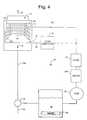
- FIG. 4is a schematic block diagram of an alternative embodiment of the system set forth in FIG. 2 wherein the ozone and treatment fluid are provided to the semiconductor workpiece along different flow paths.
- FIG. 5is a schematic block diagram of an embodiment of an apparatus for treating a semiconductor workpiece in which pressurized steam and ozone are provided in a pressurized chamber containing a semiconductor workpiece.
- FIG. 6is a schematic block diagram of an embodiment of an apparatus for treating a semiconductor workpiece in which an ultra-violet lamp is used to enhance the kinetic reactions at the surface of the workpiece.
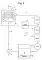
- FIG. 1One embodiment of an apparatus suitable for providing ozone and a treatment liquid for treatment of a semiconductor workpiece is illustrated in FIG. 1 .
- the treatment systemshown generally at 10 , includes a treatment chamber 15 that contains one or more workpieces 20 , such as semiconductor wafer workpieces.
- workpieces 20such as semiconductor wafer workpieces.
- the illustrated systemis directed to a batch workpiece apparatus, it will be recognized that the system is readily adaptable for use in single workpiece processing as well.
- the semiconductor workpieces 20are supported within the chamber 15 by one or more supports 25 extending from, for example, a rotor assembly 30 .
- Rotor assembly 30seals with the housing of the treatment chamber 15 to form a sealed, closed processing environment Further, rotor assembly 30 is provided so that the semiconductor workpieces 20 may be spun about axis 35 during or after treatment with the ozone and treatment liquid.
- One or mere nozzles 40are disposed within the treatment chamber 15 so as to direct a spray mixture of ozone and treatment liquid onto the surfaces of the semiconductor workpieces 20 that are to be treated
- the nozzles 40direct a spray of treatment fluid to the underside of the semiconductor workpieces 20 .
- the fluid spraymay be directed alternatively, or in addition, to the upper surface of the semiconductor workpieces 20 .
- Treatment liquid and ozoneare supplied to the nozzles 40 with the assistance of a number of system components that are uniquely arranged to provide a single fluid line comprising ozone mixed with the treating liquid.
- a reservoir 45defines a chamber 50 in which the liquid that is to be mixed with the ozone is stored.
- the chamber 50is in fluid communication with the input of a pump mechanism 55 .
- the pump mechanism 55provides the liquid under pressure along a fluid flow path, shown generally at 60 , for ultimate supply to the input of the nozzles 40 .
- the preferred treatment fluidis deionized water, but it will be recognized that other treatment fluids, such as other aqueous or non-aqueous solutions, may also be employed.
- a number of componentsare disposed along the fluid flow path 60 .
- a filter 65is disposed along the fluid flow path 60 to filter out microscopic contaminants from the treatment fluid.
- the treatment fluidstill under pressure, is provided at the output of the filter 65 along fluid flow line 70 . It is along fluid flow line 70 that ozone is injected.
- the ozoneis generated by ozone generator 75 and is supplied along fluid flow line 80 under pressure to fluid flow line 70 .
- the treatment liquid, now injected with ozoneis supplied to the input of a mixer 90 that mixes the ozone and the treatment liquid.
- the mixer 90may be static or active.
- the treatment liquid and ozoneare provided to be input of nozzles 40 which, in turn, spray the liquid on the surface of the semiconductor workpieces 20 that are to be treated and, further, introduce the ozone into the environment of the treatment chamber 15 .
- an output of the ozone generator 75may be supplied to a dispersion unit 95 disposed in the liquid chamber 50 of the reservoir 45 .
- the dispersion unit 95provides a dispersed flow of ozone through the treatment liquid to thereby add ozone to the fluid stream prior to injection of a further amount of ozone along the fluid path 60 .
- spent liquid in chamber 15is provided along fluid line 105 to, for example, a valve mechanism 110 .
- the valve mechanism 110may be operated to provide the spent liquid to either a drain output 115 or back to the liquid chamber 50 of the reservoir 45 . Repeated cycling of the treatment liquid through the system and back to the reservoir 45 assists in elevating the ozone concentration in the liquid through repeated ozone injection and/or ozone dispersion.
- FIG. 2A further embodiment of a system for delivering a fluid mixture for treating the surface of a semiconductor workpiece is illustrated in FIG. 2 .
- the system 120 of FIG. 2appears to be substantially similar to the system 10 of FIG. 1, there are significant differences.
- the system 120 of FIG. 2is based upon the recognition by the present inventors that the heating of the surfaces of the semiconductor workpieces 20 with a heated liquid that is supplied along with a flow of ozone that creates an ozonated atmosphere is highly effective in photoresist stripping, ash removal, and/or cleaning processes.
- system 120includes one or more heaters 125 that are used to heat the treatment liquid so that it is supplied to the surfaces of the semiconductor workpieces at an elevated temperature that accelerates the surface reactions.
- supports 25may include heating elements that may be used to heat the workpieces 20 .
- the chamber 15may include a heater for elevating the temperature of the chamber environment and workpieces.
- the preferred treatment liquidis deionized water since it is believed to be required to initiate the cleaning/removal reactions at the workpiece surface, probably through hydrolysis of the carbon-carbon bonds of organic molecules.
- the present inventorsrecognize that significant amounts of water can form a continuous film on the semiconductor workpiece surface. This film acts as a diffusion barrier to the ozone, thereby inhibiting reaction rates.
- Control of the boundary layer thicknessis implemented by control of the rpm of the semiconductor workpiece, vapor delivery, and controlled spraying of the treatment liquid, or a combination of one or more of these techniques. By reducing the boundary layer thickness, the ozone is allowed to diffuse to the surface of the workpieces and react with the organic materials that are to be removed.
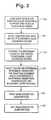
- FIG. 3illustrates one embodiment of a process that may be implemented in the system of FIG. 2 when the system 120 is used, for example, to strip photoresist from the surfaces of semiconductor workpieces.
- the workpieces 20 that are to be strippedare placed in, for example, a Teflon wafer cassette.
- This cassetteis placed in a closed environment, such as in chamber 15 .
- Chamber 15 and its corresponding componentsmay be constructed based on a spray solvent tool platform or spray acid tool platform such as those available from Semitool, Inc, of Kalispell, Mont.
- the semiconductor workpieces 20may be disposed in chamber 15 in a carrierless manner, consistent with the automated processing platform design of the MAGNUM® brand semiconductor processing tool available from Semitool, Inc.
- heated deionized wateris sprayed onto the surfaces of the semiconductor workpieces 20 .
- the heated deionized waterheats the surfaces of the semiconductor workpieces 20 as well as the enclosed environment of the chamber 15 .
- a thin liquid filmremains on the workpiece surfaces.
- a surfactantmay be added to the deionized water to assist in creating a thin liquid boundary layer on the workpiece surfaces.
- the surface boundary layer of deionized wateris controlled at step 210 using one or more techniques.
- the semiconductor workpieces 20may be rotated about axis 35 by rotor 30 to thereby generate centripetal accelerations that thin the boundary layer.
- the flow rate of the deionized watermay also be used to control the thickness of the surface boundary layer. Lowering of the flow rate results in decreased boundary layer thickness: Still further, the manner in which the deionized water is injected into the chamber 15 may be used to control the boundary layer thickness.
- Nozzles 40may be designed to provide the deionized water as micro-droplets thereby resulting in a thin boundary layer.
- ozoneis injected into the fluid flow path 60 during the water spray, or otherwise provided to the internal chamber environment of chamber 15 . If the apparatus of FIG. 2 is utilized, the injection of the ozone continues after the spray has shut off. If the workpiece surface begins to dry, a brief spray is preferably activated to replenish the liquid film on the workpiece surface. This ensures that the exposed workpiece surfaces remain wetted at all times and, further, ensures that the workpiece temperature is and remains elevated at the desired reaction temperature.
- ozoneWhile ozone has a limited solubility in the heated deionized water, the ozone is able to diffuse through the water and react with photoresist at the liquid/resist interface. It is believed that the presence of the deionized water itself further assists in the reactions by hydrolyzing the carbon bon bonds of organic deposits, such as photoresist, on the surface of the wafer.
- the higher temperaturepromotes the reaction kinetics while the high concentration of ozone in the gas phase promotes diffusion of ozone through the boundary layer film even though the high temperature of the boundary layer film does not actually have a high concentration of dissolved ozone.
- the workpiecesare subject to a rinse at 220 and are dried at step 225 .
- the workpiecesmay be sprayed with a flow of deionized water during the rinse at step 220 . They may then be subject to any one or more known drying techniques thereafter at step 225 .
- nozzles 230are disposed within the treatment chamber 15 to conduct ozone from ozone generator 75 directly into the reaction environment
- the heated treatment fluidis provided to the chamber 15 through nozzles 40 that receive the treatment fluid, such as heated deionized water, through a supply line that is separate from the ozone supply line.
- injection of ozone in fluid path 60is optional.
- FIG. 5Another embodiment of an ozone treatment system is shown generally at 250 in FIG. 5 .
- a steam boiler 260that supplies saturated steam under pressure to the process chamber 15 has replaced the pump mechanism.
- the reaction chamber 15is preferably sealed to thereby form a pressurized atmosphere for the reactions.
- saturated steam at 126 degrees Celsiuscould be generated by steam boiler 260 and supplied to reaction chamber 15 to generate a pressure of 35 psia therein during the workpiece processing.
- Ozonemay be directly injected into the chamber 15 as shown, and/or may be injected into the path 60 for concurrent supply with the steam.
- FIG. 6A still further enhancement that may be made to any one of the foregoing systems is illustrated in FIG. 6 .
- an ultra-violet lamp 300is used to irradiate the surface of the semiconductor workpiece 20 during processing. Such irradiation further enhances the reaction kdnetics.
- this irradiation techniqueis applicable to batch semiconductor workpiece processing, it is more easily and economically implemented in the illustrated single wafer processing environment where the workpiece is more easily completely exposed to the UV radiation.
- the presently disclosed apparatus and methodsmay be used to treat workpieces beyond the semiconductor workpieces described above.
- other workpiecessuch as flat panel displays, hard disk media, CD glass, etc, may also be have their surfaces treated using the foregoing apparatus and methods.
- treatment liquid for the disclosed applicationis deionized water
- other treatment liquidsmay also be used.
- acidic and basic solutionsmay be used, depending on the particular surface to be treated and the material that is to be removed.
- Treatment liquidscomprising sulfonic acid, hydrochloric acid, and ammonium hydroxide may be useful in various applications.
Landscapes
- Engineering & Computer Science (AREA)
- Physics & Mathematics (AREA)
- Condensed Matter Physics & Semiconductors (AREA)
- General Physics & Mathematics (AREA)
- Manufacturing & Machinery (AREA)
- Computer Hardware Design (AREA)
- Microelectronics & Electronic Packaging (AREA)
- Power Engineering (AREA)
- Chemical & Material Sciences (AREA)
- Chemical Kinetics & Catalysis (AREA)
- General Chemical & Material Sciences (AREA)
- Cleaning Or Drying Semiconductors (AREA)
Abstract
Description
Claims (25)
Priority Applications (1)
| Application Number | Priority Date | Filing Date | Title |
|---|---|---|---|
| US09/677,934US6267125B1 (en) | 1997-05-09 | 2000-10-03 | Apparatus and method for processing the surface of a workpiece with ozone |
Applications Claiming Priority (3)
| Application Number | Priority Date | Filing Date | Title |
|---|---|---|---|
| US08/853,649US6240933B1 (en) | 1997-05-09 | 1997-05-09 | Methods for cleaning semiconductor surfaces |
| US6131898A | 1998-04-16 | 1998-04-16 | |
| US09/677,934US6267125B1 (en) | 1997-05-09 | 2000-10-03 | Apparatus and method for processing the surface of a workpiece with ozone |
Related Parent Applications (1)
| Application Number | Title | Priority Date | Filing Date |
|---|---|---|---|
| US6131898ADivision | 1997-05-09 | 1998-04-16 |
Publications (1)
| Publication Number | Publication Date |
|---|---|
| US6267125B1true US6267125B1 (en) | 2001-07-31 |
Family
ID=26740940
Family Applications (9)
| Application Number | Title | Priority Date | Filing Date |
|---|---|---|---|
| US09/536,251Expired - LifetimeUS6701941B1 (en) | 1997-05-09 | 2000-03-27 | Method for treating the surface of a workpiece |
| US09/677,925Expired - LifetimeUS6591845B1 (en) | 1997-05-09 | 2000-10-03 | Apparatus and method for processing the surface of a workpiece with ozone |
| US09/677,929Expired - LifetimeUS6273108B1 (en) | 1997-05-09 | 2000-10-03 | Apparatus and method for processing the surface of a workpiece with ozone |
| US09/677,934Expired - LifetimeUS6267125B1 (en) | 1997-05-09 | 2000-10-03 | Apparatus and method for processing the surface of a workpiece with ozone |
| US09/837,722Expired - LifetimeUS6601594B2 (en) | 1997-05-09 | 2001-04-18 | Apparatus and method for delivering a treatment liquid and ozone to treat the surface of a workpiece |
| US09/929,437Expired - LifetimeUS6582525B2 (en) | 1997-05-09 | 2001-08-14 | Methods for processing a workpiece using steam and ozone |
| US09/929,312Expired - Fee RelatedUS6497768B2 (en) | 1997-05-09 | 2001-08-14 | Process for treating a workpiece with hydrofluoric acid and ozone |
| US10/420,659Expired - LifetimeUS6817370B2 (en) | 1997-05-09 | 2003-04-21 | Method for processing the surface of a workpiece |
| US10/998,278AbandonedUS20050072446A1 (en) | 1997-05-09 | 2004-11-23 | Process and apparatus for treating a workpiece |
Family Applications Before (3)
| Application Number | Title | Priority Date | Filing Date |
|---|---|---|---|
| US09/536,251Expired - LifetimeUS6701941B1 (en) | 1997-05-09 | 2000-03-27 | Method for treating the surface of a workpiece |
| US09/677,925Expired - LifetimeUS6591845B1 (en) | 1997-05-09 | 2000-10-03 | Apparatus and method for processing the surface of a workpiece with ozone |
| US09/677,929Expired - LifetimeUS6273108B1 (en) | 1997-05-09 | 2000-10-03 | Apparatus and method for processing the surface of a workpiece with ozone |
Family Applications After (5)
| Application Number | Title | Priority Date | Filing Date |
|---|---|---|---|
| US09/837,722Expired - LifetimeUS6601594B2 (en) | 1997-05-09 | 2001-04-18 | Apparatus and method for delivering a treatment liquid and ozone to treat the surface of a workpiece |
| US09/929,437Expired - LifetimeUS6582525B2 (en) | 1997-05-09 | 2001-08-14 | Methods for processing a workpiece using steam and ozone |
| US09/929,312Expired - Fee RelatedUS6497768B2 (en) | 1997-05-09 | 2001-08-14 | Process for treating a workpiece with hydrofluoric acid and ozone |
| US10/420,659Expired - LifetimeUS6817370B2 (en) | 1997-05-09 | 2003-04-21 | Method for processing the surface of a workpiece |
| US10/998,278AbandonedUS20050072446A1 (en) | 1997-05-09 | 2004-11-23 | Process and apparatus for treating a workpiece |
Country Status (1)
| Country | Link |
|---|---|
| US (9) | US6701941B1 (en) |
Cited By (55)
| Publication number | Priority date | Publication date | Assignee | Title |
|---|---|---|---|---|
| US20020015863A1 (en)* | 2000-04-26 | 2002-02-07 | Norihiko Nakajima | Method for cleaning a glass substrate for a magnetic recording medium, a glass substrate cleaned by such a method, and a magnetic recording medium using such a substrate |
| US6406551B1 (en) | 1999-05-14 | 2002-06-18 | Fsi International, Inc. | Method for treating a substrate with heat sensitive agents |
| US6440871B1 (en)* | 2000-08-16 | 2002-08-27 | Micron Technology, Inc. | Gas assisted method for applying resist stripper and gas-resist stripper combinations |
| US20020121287A1 (en)* | 2001-03-02 | 2002-09-05 | Gilton Terry L. | Method for removing organic material from a substrate and for oxidizing oxidizable material thereon |
| WO2002076640A1 (en)* | 2001-03-27 | 2002-10-03 | Semitool, Inc. | Vertical process reactor |
| US20020157686A1 (en)* | 1997-05-09 | 2002-10-31 | Semitool, Inc. | Process and apparatus for treating a workpiece such as a semiconductor wafer |
| US20020185225A1 (en)* | 2001-05-28 | 2002-12-12 | Tokyo Electron Limited | Substrate processing method and substrate processing apparatus |
| US6505634B2 (en)* | 2001-03-23 | 2003-01-14 | Will Be S & T Co., Ltd. | Semiconductor wafer cleaning apparatus |
| US20030051742A1 (en)* | 2001-04-19 | 2003-03-20 | Boyers David G. | Method and apparatus for treating a substrate with an ozone-solvent solution II |
| US20030084927A1 (en)* | 2001-11-08 | 2003-05-08 | Mitsubishi Denki Kabushiki Kaisha | Washer and washing method |
| US20030136429A1 (en)* | 2002-01-22 | 2003-07-24 | Semitool, Inc. | Vapor cleaning and liquid rinsing process vessel |
| US6613692B1 (en)* | 1999-07-30 | 2003-09-02 | Tokyo Electron Limited | Substrate processing method and apparatus |
| US20030192577A1 (en)* | 2002-04-11 | 2003-10-16 | Applied Materials, Inc. | Method and apparatus for wafer cleaning |
| US20040020513A1 (en)* | 1997-05-09 | 2004-02-05 | Semitool, Inc. | Methods of thinning a silicon wafer using HF and ozone |
| US6699330B1 (en)* | 1999-09-30 | 2004-03-02 | Nomura Micro Science Co., Ltd. | Method of removing contamination adhered to surfaces and apparatus used therefor |
| US20040040583A1 (en)* | 1997-05-09 | 2004-03-04 | Semitool, Inc. | Workpiece processing system |
| US20040069320A1 (en)* | 1997-05-09 | 2004-04-15 | Semitool, Inc. | Methods for cleaning semiconductor surfaces |
| US6790783B1 (en) | 1999-05-27 | 2004-09-14 | Micron Technology, Inc. | Semiconductor fabrication apparatus |
| US20040216763A1 (en)* | 1997-05-09 | 2004-11-04 | Semitool, Inc. | Process and apparatus for treating a workpiece using ozone |
| US20040221877A1 (en)* | 1997-05-09 | 2004-11-11 | Semitool, Inc. | Process and apparatus for treating a workpiece with gases |
| US20040261823A1 (en)* | 2003-06-27 | 2004-12-30 | Lam Research Corporation | Method and apparatus for removing a target layer from a substrate using reactive gases |
| US20050034745A1 (en)* | 1997-05-09 | 2005-02-17 | Semitool, Inc. | Processing a workpiece with ozone and a halogenated additive |
| US6869487B1 (en) | 1997-05-09 | 2005-03-22 | Semitool, Inc. | Process and apparatus for treating a workpiece such as a semiconductor wafer |
| US20050072446A1 (en)* | 1997-05-09 | 2005-04-07 | Bergman Eric J. | Process and apparatus for treating a workpiece |
| US20050133060A1 (en)* | 2003-12-23 | 2005-06-23 | Larios John M.D. | Method and apparatus for cleaning semiconductor wafers using compressed and/or pressurized foams, bubbles, and/or liquids |
| US20050133067A1 (en)* | 1997-05-09 | 2005-06-23 | Bergman Eric J. | Processing a workpiece using water, a base, and ozone |
| US20050215063A1 (en)* | 1997-05-09 | 2005-09-29 | Bergman Eric J | System and methods for etching a silicon wafer using HF and ozone |
| US20050236363A1 (en)* | 1997-05-09 | 2005-10-27 | Bergman Eric J | System and methods for polishing a wafer |
| US20060107976A1 (en)* | 1999-10-19 | 2006-05-25 | Boyers David G | Apparatus for treating a substrate with an ozone-solvent solution |
| US20060128590A1 (en)* | 2003-06-27 | 2006-06-15 | Lam Research Corporation | Method for removing contamination from a substrate and for making a cleaning solution |
| US20060283486A1 (en)* | 2005-06-15 | 2006-12-21 | Lam Research Corporation | Method and apparatus for cleaning a substrate using non-newtonian fluids |
| US20060285930A1 (en)* | 2005-06-15 | 2006-12-21 | Lam Research Corporation | Method and apparatus for transporting a substrate using non-Newtonian fluid |
| US20070068552A1 (en)* | 2005-09-23 | 2007-03-29 | Bruce Willing | Ozonation for elimination of bacteria for wet processing systems |
| US20070079848A1 (en)* | 2003-06-27 | 2007-04-12 | Lam Research Corporation | Method and apparatus for removing contamination from substrate |
| US20070087950A1 (en)* | 2003-06-27 | 2007-04-19 | Lam Research Corporation | Method and system for using a two-phases substrate cleaning compound |
| US20070084485A1 (en)* | 2003-06-27 | 2007-04-19 | Freer Erik M | Method and apparatus for cleaning a semiconductor substrate |
| US20070084483A1 (en)* | 2003-06-27 | 2007-04-19 | Freer Erik M | Method and apparatus for cleaning a semiconductor substrate |
| US20070151583A1 (en)* | 2005-12-30 | 2007-07-05 | Lam Research Corporation | Method and apparatus for particle removal |
| US20070155640A1 (en)* | 2005-12-30 | 2007-07-05 | Lam Research Corporation | Substrate preparation using stabilized fluid solutions and methods for making stable fluid solutions |
| US20080148595A1 (en)* | 2006-12-20 | 2008-06-26 | Lam Research Corporation | Method and apparatus for drying substrates using a surface tensions reducing gas |
| US20080271749A1 (en)* | 2007-05-02 | 2008-11-06 | Lam Research Corporation | Substrate cleaning technique employing multi-phase solution |
| US20090114249A1 (en)* | 2007-02-08 | 2009-05-07 | Lam Research Corporation | System and method for contained chemical surface treatment |
| US20090205677A1 (en)* | 2002-04-11 | 2009-08-20 | Randhir Thakur | Method and apparatus for wafer cleaning |
| US20090308413A1 (en)* | 2005-12-30 | 2009-12-17 | Lam Research Corporation | Apparatus and system for cleaning a substrate |
| US20090308410A1 (en)* | 2005-12-30 | 2009-12-17 | Lam Research Corporation | Method and material for cleaning a substrate |
| EP2081604A4 (en)* | 2006-10-25 | 2010-12-15 | Agrimond Usa Corp | Ozone disinfection apparatus |
| US7913703B1 (en) | 2003-06-27 | 2011-03-29 | Lam Research Corporation | Method and apparatus for uniformly applying a multi-phase cleaning solution to a substrate |
| US20110305839A1 (en)* | 2010-06-09 | 2011-12-15 | Kurita Water Industries Ltd | Ozone gas treatment process and treatment apparatus |
| US8323420B2 (en) | 2005-06-30 | 2012-12-04 | Lam Research Corporation | Method for removing material from semiconductor wafer and apparatus for performing the same |
| US8758522B2 (en) | 2007-12-14 | 2014-06-24 | Lam Research Corporation | Method and apparatus for removing contaminants from substrate |
| US9919939B2 (en) | 2011-12-06 | 2018-03-20 | Delta Faucet Company | Ozone distribution in a faucet |
| US10002771B1 (en) | 2017-10-10 | 2018-06-19 | Applied Materials, Inc. | Methods for chemical mechanical polishing (CMP) processing with ozone |
| US11458214B2 (en) | 2015-12-21 | 2022-10-04 | Delta Faucet Company | Fluid delivery system including a disinfectant device |
| US11992585B2 (en) | 2020-03-13 | 2024-05-28 | Julian HENLEY | Electro-ionic devices for improved protection from airborne biopathogens |
| US12017232B2 (en) | 2020-03-13 | 2024-06-25 | Julian HENLEY | Electro-ionic mask devices for improved protection from airborne biopathogens |
Families Citing this family (101)
| Publication number | Priority date | Publication date | Assignee | Title |
|---|---|---|---|---|
| US20050194356A1 (en)* | 1997-05-09 | 2005-09-08 | Semitool, Inc. | Removing photoresist from a workpiece using water and ozone and a photoresist penetrating additive |
| US6715944B2 (en)* | 1998-11-12 | 2004-04-06 | Mitsubishi Denki Kabushiki Kaisha | Apparatus for removing photoresist film |
| JP2000147793A (en)* | 1998-11-12 | 2000-05-26 | Mitsubishi Electric Corp | Photoresist film removing method and apparatus therefor |
| JP3869566B2 (en)* | 1998-11-13 | 2007-01-17 | 三菱電機株式会社 | Photoresist film removal method and apparatus |
| JP3395696B2 (en) | 1999-03-15 | 2003-04-14 | 日本電気株式会社 | Wafer processing apparatus and wafer processing method |
| JP2001118817A (en)* | 1999-08-12 | 2001-04-27 | Uct Kk | Surface-purifying device and method |
| US6408535B1 (en)* | 1999-08-26 | 2002-06-25 | Semitool, Inc. | Ozone conversion in semiconductor manufacturing |
| US6758938B1 (en)* | 1999-08-31 | 2004-07-06 | Micron Technology, Inc. | Delivery of dissolved ozone |
| US6634368B1 (en)* | 1999-11-12 | 2003-10-21 | Texas Instruments Incorporated | Application of ozonated DI water to scrubbers for resist strip and particle removal processes |
| US6588437B1 (en)* | 1999-11-15 | 2003-07-08 | Agere Systems Inc. | System and method for removal of material |
| US6686297B1 (en) | 2000-08-17 | 2004-02-03 | Georg Gogg | Method of manufacturing a semiconductor device and apparatus to be used therefore |
| WO2002027775A1 (en)* | 2000-09-28 | 2002-04-04 | Mitsubishi Denki Kabushiki Kaisha | Method and apparatus for treating wafer |
| TW471010B (en)* | 2000-09-28 | 2002-01-01 | Applied Materials Inc | Wafer cleaning equipment |
| JP4014127B2 (en)* | 2000-10-04 | 2007-11-28 | 東京エレクトロン株式会社 | Substrate processing method and substrate processing apparatus |
| US6532974B2 (en) | 2001-04-06 | 2003-03-18 | Akrion Llc | Process tank with pressurized mist generation |
| US7841355B2 (en)* | 2005-06-16 | 2010-11-30 | Evrio, Inc. | Modular system including shaft segments having configuration and breakdown attachments |
| US7802582B2 (en)* | 2006-07-10 | 2010-09-28 | Evrio, Inc. | System for concealment and shelter with structure for rapid setup and tight skin |
| US8397738B2 (en)* | 2001-06-04 | 2013-03-19 | Evrio, Inc. | Modular system for concealment and shelter |
| ATE354175T1 (en)* | 2001-06-12 | 2007-03-15 | Akrion Technologies Inc | MEGASONIC CLEANING AND DRYING DEVICE |
| US6579810B2 (en)* | 2001-06-21 | 2003-06-17 | Macronix International Co. Ltd. | Method of removing a photoresist layer on a semiconductor wafer |
| JP3950319B2 (en)* | 2001-10-31 | 2007-08-01 | Hoya株式会社 | Method for cleaning glass substrate for information recording medium, method for producing glass substrate for information recording medium, and method for producing information recording medium |
| JP3717846B2 (en)* | 2001-12-25 | 2005-11-16 | Hoya株式会社 | Method for manufacturing plastic lens having antireflection film |
| US20030127425A1 (en)* | 2002-01-07 | 2003-07-10 | Hirohiko Nishiki | System and method for etching resin with an ozone wet etching process |
| US7371467B2 (en) | 2002-01-08 | 2008-05-13 | Applied Materials, Inc. | Process chamber component having electroplated yttrium containing coating |
| US20030139057A1 (en)* | 2002-01-18 | 2003-07-24 | Richard Novak | Process and apparatus for removal of photoresist from semiconductor wafers |
| JP2003249476A (en)* | 2002-02-22 | 2003-09-05 | Matsushita Electric Ind Co Ltd | Wafer cleaning method |
| US20040154641A1 (en)* | 2002-05-17 | 2004-08-12 | P.C.T. Systems, Inc. | Substrate processing apparatus and method |
| US20040159335A1 (en)* | 2002-05-17 | 2004-08-19 | P.C.T. Systems, Inc. | Method and apparatus for removing organic layers |
| AU2003243974A1 (en)* | 2002-06-25 | 2004-01-06 | Tokyo Electron Limited | Substrate processing device |
| ATE353475T1 (en)* | 2002-10-11 | 2007-02-15 | Soitec Silicon On Insulator | METHOD AND DEVICE FOR PRODUCING AN ADHESIVE SUBSTRATE SURFACE |
| AU2003276093A1 (en)* | 2002-10-14 | 2004-05-04 | Sez Ag | Method for generating oxide layers on semiconductor substrates |
| US7051743B2 (en)* | 2002-10-29 | 2006-05-30 | Yong Bae Kim | Apparatus and method for cleaning surfaces of semiconductor wafers using ozone |
| US7022193B2 (en)* | 2002-10-29 | 2006-04-04 | In Kwon Jeong | Apparatus and method for treating surfaces of semiconductor wafers using ozone |
| DE60320665T2 (en)* | 2002-12-10 | 2009-05-28 | Semitool, Inc., Kalispell | WORK PIECE PROCESSING SYSTEM |
| US20040115957A1 (en)* | 2002-12-17 | 2004-06-17 | Taiwan Semiconductor Manufacturing Co., Ltd. | Apparatus and method for enhancing wet stripping of photoresist |
| FR2852869B1 (en)* | 2003-03-26 | 2006-07-14 | Soitec Silicon On Insulator | SURFACE TREATMENT OF A SEMICONDUCTOR WAFER BEFORE COLLAGE |
| US7071077B2 (en)* | 2003-03-26 | 2006-07-04 | S.O.I.Tec Silicon On Insulator Technologies S.A. | Method for preparing a bonding surface of a semiconductor layer of a wafer |
| WO2004112093A2 (en)* | 2003-06-06 | 2004-12-23 | P.C.T. Systems, Inc. | Method and apparatus to process substrates with megasonic energy |
| US7279431B2 (en)* | 2003-06-18 | 2007-10-09 | Semitool, Inc. | Vapor phase etching MEMS devices |
| TWI377453B (en)* | 2003-07-31 | 2012-11-21 | Akrion Technologies Inc | Process sequence for photoresist stripping and/or cleaning of photomasks for integrated circuit manufacturing |
| KR100546386B1 (en)* | 2003-10-10 | 2006-01-26 | 삼성전자주식회사 | ST film formation method of a semiconductor device capable of preventing voids |
| US20050090856A1 (en)* | 2003-10-27 | 2005-04-28 | Scimed Life Systems, Inc. | Vasco-occlusive devices with bioactive elements |
| US7645292B2 (en)* | 2003-10-27 | 2010-01-12 | Boston Scientific Scimed, Inc. | Vaso-occlusive devices with in-situ stiffening elements |
| US7022610B2 (en)* | 2003-12-22 | 2006-04-04 | Taiwan Semiconductor Manufacturing Company | Wet cleaning method to eliminate copper corrosion |
| CN100377312C (en)* | 2004-03-03 | 2008-03-26 | 鸿富锦精密工业(深圳)有限公司 | Etching system and pure water adding device thereof |
| US7122484B2 (en)* | 2004-04-28 | 2006-10-17 | Taiwan Semiconductor Manufacturing Company, Ltd. | Process for removing organic materials during formation of a metal interconnect |
| US20050252547A1 (en)* | 2004-05-11 | 2005-11-17 | Applied Materials, Inc. | Methods and apparatus for liquid chemical delivery |
| JP4753596B2 (en)* | 2004-05-19 | 2011-08-24 | 大日本スクリーン製造株式会社 | Substrate processing equipment |
| US20050274393A1 (en)* | 2004-06-09 | 2005-12-15 | Taiwan Semiconductor Manufacturing Co., Ltd. | Wafer clean process |
| US20050284375A1 (en)* | 2004-06-24 | 2005-12-29 | Kodjo Leeds | Method and apparatus for processing a workpiece |
| US20050284568A1 (en)* | 2004-06-28 | 2005-12-29 | International Business Machines Corporation | Removing unwanted film from wafer edge region with reactive gas jet |
| US7781152B2 (en)* | 2004-07-28 | 2010-08-24 | Headway Technologies, Inc. | Ozone-assisted lithography process with image enhancement for CPP head manufacturing |
| US7288489B2 (en)* | 2004-08-20 | 2007-10-30 | Semitool, Inc. | Process for thinning a semiconductor workpiece |
| US20060040111A1 (en)* | 2004-08-20 | 2006-02-23 | Dolechek Kert L | Process chamber and system for thinning a semiconductor workpiece |
| US7354649B2 (en) | 2004-08-20 | 2008-04-08 | Semitool, Inc. | Semiconductor workpiece |
| US20060046499A1 (en)* | 2004-08-20 | 2006-03-02 | Dolechek Kert L | Apparatus for use in thinning a semiconductor workpiece |
| US7193295B2 (en)* | 2004-08-20 | 2007-03-20 | Semitool, Inc. | Process and apparatus for thinning a semiconductor workpiece |
| US7806988B2 (en)* | 2004-09-28 | 2010-10-05 | Micron Technology, Inc. | Method to address carbon incorporation in an interpoly oxide |
| JP4661784B2 (en)* | 2004-09-30 | 2011-03-30 | 信越半導体株式会社 | Method for cleaning SOI wafer |
| US7604780B2 (en)* | 2004-11-11 | 2009-10-20 | Agrimond Usa Corporation | Ozone disinfection apparatus |
| KR20060072498A (en)* | 2004-12-23 | 2006-06-28 | 동부일렉트로닉스 주식회사 | Semiconductor device and its manufacturing method |
| US20060254611A1 (en)* | 2005-04-12 | 2006-11-16 | Harald Koster | Acid-free cleaning process for substrates, in particular masks and mask blanks |
| JP2006352075A (en)* | 2005-05-17 | 2006-12-28 | Sumitomo Electric Ind Ltd | Nitride-based compound semiconductor, compound semiconductor cleaning method, manufacturing method thereof, and substrate |
| US20110018105A1 (en)* | 2005-05-17 | 2011-01-27 | Sumitomo Electric Industries, Ltd. | Nitride-based compound semiconductor device, compound semiconductor device, and method of producing the devices |
| US20060263281A1 (en)* | 2005-05-20 | 2006-11-23 | Dial Discoveries Llc | Systems and methods for treatment of various environments by application of ozone and steam |
| US20070012335A1 (en)* | 2005-07-18 | 2007-01-18 | Chang Hsiao C | Photomask cleaning using vacuum ultraviolet (VUV) light cleaning |
| JP4977999B2 (en)* | 2005-11-21 | 2012-07-18 | 株式会社Sumco | Manufacturing method of bonded substrate and bonded substrate manufactured by the method |
| CN101389415A (en)* | 2006-02-22 | 2009-03-18 | 赛迈有限公司 | Single side workpiece processing |
| US20070261718A1 (en)* | 2006-05-10 | 2007-11-15 | Rubinder Randhawa | Method and apparatus for ozone-enhanced cleaning of flat objects with pulsed liquid jet |
| US20080029123A1 (en)* | 2006-08-02 | 2008-02-07 | Brian Aegerter | Sonic and chemical wafer processor |
| US7653954B2 (en)* | 2006-12-20 | 2010-02-02 | Hill-Rom Services, Inc. | Lift system for a patient-support apparatus |
| KR100925029B1 (en)* | 2006-12-27 | 2009-11-03 | 주식회사 하이닉스반도체 | Manufacturing method of semiconductor device |
| US8741066B2 (en) | 2007-02-16 | 2014-06-03 | Akrion Systems, Llc | Method for cleaning substrates utilizing surface passivation and/or oxide layer growth to protect from pitting |
| KR101532224B1 (en) | 2007-05-18 | 2015-06-30 | 티이엘 에프에스아이, 인코포레이티드 | Process for treatment of substrates with water vapor or steam |
| DE102007027112B4 (en)* | 2007-06-13 | 2011-06-22 | Siltronic AG, 81737 | Process for cleaning, drying and hydrophilizing a semiconductor wafer |
| KR100899426B1 (en)* | 2007-09-14 | 2009-05-27 | 삼성모바일디스플레이주식회사 | Manufacturing method of organic electroluminescent display |
| DE102007044787A1 (en)* | 2007-09-19 | 2009-04-02 | Siltronic Ag | Method for cleaning a semiconductor wafer |
| JP2009081366A (en)* | 2007-09-27 | 2009-04-16 | Elpida Memory Inc | Batch processing apparatus |
| US20090087993A1 (en)* | 2007-09-28 | 2009-04-02 | Steven Maxwell | Methods and apparatus for cost-effectively increasing feature density using a mask shrinking process with double patterning |
| US20090085169A1 (en)* | 2007-09-28 | 2009-04-02 | Willy Rachmady | Method of achieving atomically smooth sidewalls in deep trenches, and high aspect ratio silicon structure containing atomically smooth sidewalls |
| DE102007058503B4 (en) | 2007-12-05 | 2011-08-25 | Siltronic AG, 81737 | Process for the wet-chemical treatment of a semiconductor wafer |
| US20100024847A1 (en)* | 2008-08-01 | 2010-02-04 | Breese Ronald G | Semiconductor wafer cleaning with dilute acids |
| US20100084261A1 (en)* | 2008-10-07 | 2010-04-08 | China Institute Of Technology | Method for fabricating polymeric wavelength filter |
| FR2951372B1 (en)* | 2009-10-20 | 2011-12-09 | Hill Rom Sas | HOSPITAL OR ACCOMMODATION BED WITH ADJUSTABLE SLEEPING PLAN |
| US20110130009A1 (en)* | 2009-11-30 | 2011-06-02 | Lam Research Ag | Method and apparatus for surface treatment using a mixture of acid and oxidizing gas |
| TW201206857A (en)* | 2010-06-17 | 2012-02-16 | Imec | Method for passivating a silicon surface |
| US8709165B2 (en) | 2010-12-03 | 2014-04-29 | Lam Research Ag | Method and apparatus for surface treatment using inorganic acid and ozone |
| US8940103B2 (en) | 2012-03-06 | 2015-01-27 | Tokyo Electron Limited | Sequential stage mixing for single substrate strip processing |
| US9075318B2 (en) | 2012-03-07 | 2015-07-07 | Tokyo Electron Limited | Sequential stage mixing for a resist batch strip process |
| US8871108B2 (en) | 2013-01-22 | 2014-10-28 | Tel Fsi, Inc. | Process for removing carbon material from substrates |
| WO2014117864A1 (en)* | 2013-02-01 | 2014-08-07 | Ruf Gmbh & Co Kg | Feeding device for feeding lumpy material into a briquetting press |
| US9881816B2 (en)* | 2013-02-01 | 2018-01-30 | Taiwan Semiconductor Manufacturing Company, Ltd. | Cleaning composition and method for semiconductor device fabrication |
| HRP20231107T1 (en)* | 2013-10-22 | 2023-12-22 | Bechtel Energy Technologies & Solutions, Inc. | System for on-line pigging and spalling of coker furnace outlets |
| US20150354403A1 (en)* | 2014-06-05 | 2015-12-10 | General Electric Company | Off-line wash systems and methods for a gas turbine engine |
| US20170018423A1 (en)* | 2015-07-15 | 2017-01-19 | Oem Group, Inc. | Apparatus and Method for Processing the Surface of a Workpiece Comprised of Sensitive Materials with an Ozone and Carbon Dioxide Treating Fluid |
| JP6593920B2 (en)* | 2015-08-18 | 2019-10-23 | 株式会社Screenホールディングス | Substrate processing method and substrate processing apparatus |
| US20180166300A1 (en)* | 2016-12-13 | 2018-06-14 | Lam Research Ag | Point-of-use mixing systems and methods for controlling temperatures of liquids dispensed at a substrate |
| JP7013710B2 (en)* | 2017-08-07 | 2022-02-01 | 住友電気工業株式会社 | Manufacturing method of nitride semiconductor transistor |
| CN109107974B (en)* | 2018-07-20 | 2020-08-11 | 横店集团东磁股份有限公司 | Cleaning method of quartz device for solar cell preparation |
| US11673830B2 (en)* | 2020-11-11 | 2023-06-13 | Applied Materials, Inc. | Glass carrier cleaning using ozone |
| US11728185B2 (en) | 2021-01-05 | 2023-08-15 | Applied Materials, Inc. | Steam-assisted single substrate cleaning process and apparatus |
Citations (37)
| Publication number | Priority date | Publication date | Assignee | Title |
|---|---|---|---|---|
| JPS5212063A (en) | 1975-07-15 | 1977-01-29 | Matsushita Electric Works Ltd | Hair curling apparatus |
| US4695327A (en) | 1985-06-13 | 1987-09-22 | Purusar Corporation | Surface treatment to remove impurities in microrecesses |
| US4778532A (en) | 1985-06-24 | 1988-10-18 | Cfm Technologies Limited Partnership | Process and apparatus for treating wafers with process fluids |
| EP0344764A2 (en) | 1988-06-01 | 1989-12-06 | Wacker-Chemitronic Gesellschaft für Elektronik-Grundstoffe mbH | Process for the wet-chemical surface treatment of semiconductor chips |
| US4899767A (en) | 1984-05-21 | 1990-02-13 | Cfm Technologies, Inc. | Method and system for fluid treatment of semiconductor wafers |
| US4974530A (en) | 1989-11-16 | 1990-12-04 | Energy And Environmental Research | Apparatus and methods for incineration of toxic organic compounds |
| US5032218A (en)* | 1988-08-12 | 1991-07-16 | Alameda Instruments, Inc. | Sulfuric acid reprocessor |
| US5055138A (en) | 1988-07-08 | 1991-10-08 | Isc Chemicals Limited | Cleaning and drying of electronic assemblies |
| US5071485A (en) | 1990-09-11 | 1991-12-10 | Fusion Systems Corporation | Method for photoresist stripping using reverse flow |
| US5120370A (en) | 1991-04-01 | 1992-06-09 | Shinichi Mori | Cleaning process |
| US5181985A (en) | 1988-06-01 | 1993-01-26 | Wacker-Chemitronic Gesellschaft Fur Elektronik-Grundstoffe Mbh | Process for the wet-chemical surface treatment of semiconductor wafers |
| EP0548596A2 (en) | 1991-11-29 | 1993-06-30 | CHLORINE ENGINEERS CORP., Ltd. | Method and apparatus for cleaning substrate |
| US5232511A (en) | 1990-05-15 | 1993-08-03 | Semitool, Inc. | Dynamic semiconductor wafer processing using homogeneous mixed acid vapors |
| US5234540A (en) | 1992-04-30 | 1993-08-10 | Submicron Systems, Inc. | Process for etching oxide films in a sealed photochemical reactor |
| US5235995A (en) | 1989-03-27 | 1993-08-17 | Semitool, Inc. | Semiconductor processor apparatus with dynamic wafer vapor treatment and particulate volatilization |
| US5244000A (en) | 1991-11-13 | 1993-09-14 | Hughes Aircraft Company | Method and system for removing contaminants |
| US5248380A (en) | 1990-11-06 | 1993-09-28 | Mitsubishi Denki Kabushiki Kaisha | Method of treating surface of rotating wafer using surface treating gas |
| US5308745A (en) | 1992-11-06 | 1994-05-03 | J. T. Baker Inc. | Alkaline-containing photoresist stripping compositions producing reduced metal corrosion with cross-linked or hardened resist resins |
| US5378317A (en) | 1990-10-09 | 1995-01-03 | Chlorine Engineers Corp., Ltd. | Method for removing organic film |
| US5415191A (en) | 1991-01-28 | 1995-05-16 | Kabushiki Kaisha Toshiba | Arrangement for cleaning semiconductor wafers using mixer |
| GB2287827A (en) | 1994-03-25 | 1995-09-27 | Nec Corp | Wet processing of semiconductor substrates |
| US5464480A (en) | 1993-07-16 | 1995-11-07 | Legacy Systems, Inc. | Process and apparatus for the treatment of semiconductor wafers in a fluid |
| EP0702399A1 (en) | 1994-09-14 | 1996-03-20 | Siemens Aktiengesellschaft | Process for wet chemical removal of contaminants from semiconductor crystal surfaces |
| US5503708A (en) | 1992-11-27 | 1996-04-02 | Hitachi, Ltd. | Method of and apparatus for removing an organic film |
| US5520744A (en) | 1993-05-17 | 1996-05-28 | Dainippon Screen Manufacturing Co., Ltd. | Device for rinsing and drying substrate |
| US5632847A (en) | 1994-04-26 | 1997-05-27 | Chlorine Engineers Corp., Ltd. | Film removing method and film removing agent |
| US5647386A (en) | 1994-10-04 | 1997-07-15 | Entropic Systems, Inc. | Automatic precision cleaning apparatus with continuous on-line monitoring and feedback |
| US5658615A (en) | 1993-03-25 | 1997-08-19 | Tokyo Electron Limited | Method of forming coating film and apparatus therefor |
| US5705089A (en) | 1992-03-11 | 1998-01-06 | Mitsubishi Gas Chemical Company, Inc. | Cleaning fluid for semiconductor substrate |
| US5714203A (en) | 1995-08-23 | 1998-02-03 | Ictop Entwicklungs Gmbh | Procedure for the drying of silicon |
| US5803982A (en) | 1996-10-15 | 1998-09-08 | Ez Environmental Solutions Corporation | Pressure washing apparatus with ozone generator |
| US5858107A (en) | 1998-01-07 | 1999-01-12 | Raytheon Company | Liquid carbon dioxide cleaning using jet edge sonic whistles at low temperature |
| US5896875A (en) | 1995-09-01 | 1999-04-27 | Matsushita Electronics Corporation | Equipment for cleaning, etching and drying semiconductor wafer and its using method |
| US5911837A (en) | 1993-07-16 | 1999-06-15 | Legacy Systems, Inc. | Process for treatment of semiconductor wafers in a fluid |
| US5944907A (en) | 1995-03-06 | 1999-08-31 | Ohmi; Tadahiro | Cleaning device and method |
| US5964954A (en) | 1993-11-05 | 1999-10-12 | Tokyo Electron Limited | Double-sided substrate cleaning apparatus and cleaning method using the same |
| US5971368A (en) | 1997-10-29 | 1999-10-26 | Fsi International, Inc. | System to increase the quantity of dissolved gas in a liquid and to maintain the increased quantity of dissolved gas in the liquid until utilized |
Family Cites Families (96)
| Publication number | Priority date | Publication date | Assignee | Title |
|---|---|---|---|---|
| US3226406A (en)* | 1963-01-03 | 1965-12-28 | Thomas K Miwa | Wax ester substitute for jojoba oil from the seed of limnanthes douglash |
| JPS5275181A (en)* | 1975-12-13 | 1977-06-23 | Sony Corp | Formation of oxide film |
| FR2341830A1 (en)* | 1976-02-19 | 1977-09-16 | Air Ind | INSTALLATION FOR THE CONTINUOUS HEAT TREATMENT OF A RUNNING PRODUCT IN AN ENCLOSURE |
| US4186032A (en)* | 1976-09-23 | 1980-01-29 | Rca Corp. | Method for cleaning and drying semiconductors |
| US4064885A (en)* | 1976-10-26 | 1977-12-27 | Branson Ultrasonics Corporation | Apparatus for cleaning workpieces by ultrasonic energy |
| JPS5434751A (en) | 1977-08-24 | 1979-03-14 | Hitachi Ltd | Washing method for silicon wafer |
| JPS60210840A (en)* | 1984-03-06 | 1985-10-23 | Fujitsu Ltd | Spinning proccessor |
| JPS614232A (en) | 1984-06-19 | 1986-01-10 | Nec Corp | Cleaning method of semiconductor substrate |
| US4749440A (en)* | 1985-08-28 | 1988-06-07 | Fsi Corporation | Gaseous process and apparatus for removing films from substrates |
| JPS62117330A (en) | 1985-11-18 | 1987-05-28 | Sanyo Electric Co Ltd | Washing method for semiconductor wafer |
| JPS648630A (en) | 1986-09-22 | 1989-01-12 | Tokyo Electron Ltd | Cleaning method |
| JPS63110732A (en) | 1986-10-29 | 1988-05-16 | Nec Corp | Washing method for semiconductor substrate |
| US4817652A (en)* | 1987-03-26 | 1989-04-04 | Regents Of The University Of Minnesota | System for surface and fluid cleaning |
| JPS6442129A (en)* | 1987-08-10 | 1989-02-14 | Hitachi Ltd | Cleaning and removal of organic substance |
| US5105556A (en)* | 1987-08-12 | 1992-04-21 | Hitachi, Ltd. | Vapor washing process and apparatus |
| JPH01179327A (en) | 1988-01-06 | 1989-07-17 | Hitachi Ltd | Ashing |
| JPH01189921A (en) | 1988-01-26 | 1989-07-31 | Mitsubishi Electric Corp | Resist removal equipment |
| JPH0724265B2 (en)* | 1988-04-13 | 1995-03-15 | 日本電気株式会社 | Semiconductor substrate cleaning equipment |
| JPH06103685B2 (en) | 1989-05-06 | 1994-12-14 | 大日本スクリーン製造株式会社 | Substrate cleaning method and apparatus |
| US5246526A (en)* | 1989-06-29 | 1993-09-21 | Hitachi, Ltd. | Surface treatment apparatus |
| JPH0341729A (en) | 1989-07-07 | 1991-02-22 | Tokyo Electron Ltd | Substrate cleaning |
| FI84764C (en)* | 1989-09-25 | 1992-01-10 | Labsystems Oy | SPOLNINGSANORDNING. |
| US5063609A (en)* | 1989-10-11 | 1991-11-05 | Applied Materials, Inc. | Steam generator |
| US5039349A (en)* | 1990-05-18 | 1991-08-13 | Veriflo Corporation | Method and apparatus for cleaning surfaces to absolute or near-absolute cleanliness |
| JPH0719739B2 (en)* | 1990-09-10 | 1995-03-06 | 信越半導体株式会社 | Bonded wafer manufacturing method |
| JPH04125927A (en) | 1990-09-18 | 1992-04-27 | Fujitsu Ltd | Substrate cleaning method |
| US5832177A (en)* | 1990-10-05 | 1998-11-03 | Fujitsu Limited | Method for controlling apparatus for supplying steam for ashing process |
| JP2820792B2 (en)* | 1990-11-29 | 1998-11-05 | 株式会社神戸製鋼所 | Method for producing dimethylnaphthalene |
| JPH04298038A (en)* | 1991-03-27 | 1992-10-21 | Hitachi Cable Ltd | Wafer cleaning method |
| JPH04302144A (en)* | 1991-03-29 | 1992-10-26 | Hitachi Ltd | Cleaning method |
| JPH04302145A (en) | 1991-03-29 | 1992-10-26 | Hitachi Ltd | Cleaning method |
| WO1992022084A1 (en)* | 1991-05-21 | 1992-12-10 | Advantage Production Technology, Inc. | Organic preclean for improving vapor phase wafer etch uniformity |
| JP2654874B2 (en) | 1991-06-19 | 1997-09-17 | 日立造船株式会社 | Substrate cleaning method |
| JPH051993A (en)* | 1991-06-26 | 1993-01-08 | Ishikawajima Harima Heavy Ind Co Ltd | Device for measuring the orientation of strip-shaped fibers |
| JPH0513398A (en) | 1991-07-05 | 1993-01-22 | Hitachi Zosen Corp | Substrate cleaning method |
| JP3069400B2 (en)* | 1991-07-23 | 2000-07-24 | ナカ工業株式会社 | Structure of floor panel support leg attachment part |
| US5147499A (en)* | 1991-07-24 | 1992-09-15 | Applied Materials, Inc. | Process for removal of residues remaining after etching polysilicon layer in formation of integrated circuit structure |
| US5326406A (en)* | 1991-07-31 | 1994-07-05 | Kawasaki Steel Corporation | Method of cleaning semiconductor substrate and apparatus for carrying out the same |
| JPH05109686A (en) | 1991-10-14 | 1993-04-30 | Nippon Steel Corp | Method and apparatus for cleaning silicon wafer |
| JPH05134397A (en)* | 1991-11-14 | 1993-05-28 | Nikon Corp | Glass substrate cleaning method and cleaning device |
| JPH05259139A (en) | 1992-03-16 | 1993-10-08 | Hitachi Ltd | Cleaning apparatus |
| JP2956347B2 (en) | 1992-03-31 | 1999-10-04 | 日本電気株式会社 | Semiconductor substrate cleaning method |
| JPH06168922A (en)* | 1992-06-25 | 1994-06-14 | Texas Instr Inc <Ti> | Vapor etching method of silicon |
| US5366757A (en)* | 1992-10-30 | 1994-11-22 | International Business Machines Corporation | In situ resist control during spray and spin in vapor |
| JPH06204130A (en) | 1992-12-28 | 1994-07-22 | Mitsubishi Electric Corp | Pattern formation method |
| US5922624A (en)* | 1993-05-13 | 1999-07-13 | Imec Vzw | Method for semiconductor processing using mixtures of HF and carboxylic acid |
| US5447640A (en)* | 1993-06-28 | 1995-09-05 | Permelec Electrode Ltd. | Method and apparatus for sterilization of and treatment with ozonized water |
| JPH0747377A (en)* | 1993-08-06 | 1995-02-21 | Permelec Electrode Ltd | Method for treating ozone water and device therefor |
| US5730806A (en)* | 1993-08-30 | 1998-03-24 | The United States Of America As Represented By The Administrator Of The National Aeronautics & Space Administration | Gas-liquid supersonic cleaning and cleaning verification spray system |
| JPH07159980A (en) | 1993-12-06 | 1995-06-23 | Nikon Corp | Substrate cleaning equipment |
| US5600838A (en)* | 1994-01-18 | 1997-02-04 | Sybase, Inc. | Object oriented dispatch and supercall process and arrangement |
| GB9402486D0 (en)* | 1994-02-09 | 1994-03-30 | Electrotech Ltd | Forming a layer |
| JP3080834B2 (en)* | 1994-03-30 | 2000-08-28 | 株式会社東芝 | Semiconductor substrate cleaning equipment |
| JPH088222A (en) | 1994-06-22 | 1996-01-12 | Sony Corp | Spin processor |
| US5500744A (en)* | 1994-08-05 | 1996-03-19 | Miles Inc. | Method and appparatus for image scaling using parallel incremental interpolation |
| DE19522525A1 (en)* | 1994-10-04 | 1996-04-11 | Kunze Concewitz Horst Dipl Phy | Method and device for fine cleaning of surfaces |
| JPH08238463A (en)* | 1995-03-03 | 1996-09-17 | Ebara Corp | Cleaning method and cleaning device |
| AT405225B (en)* | 1995-05-02 | 1999-06-25 | Sez Semiconduct Equip Zubehoer | DEVICE FOR TREATING APPROXIMATELY ROUND OR DISC-SHAPED OBJECTS, IN PARTICULAR SILICON WAFERS |
| US5950643A (en)* | 1995-09-06 | 1999-09-14 | Miyazaki; Takeshiro | Wafer processing system |
| US5954911A (en)* | 1995-10-12 | 1999-09-21 | Semitool, Inc. | Semiconductor processing using vapor mixtures |
| US5975098A (en)* | 1995-12-21 | 1999-11-02 | Dainippon Screen Mfg. Co., Ltd. | Apparatus for and method of cleaning substrate |
| US5749975A (en)* | 1995-12-28 | 1998-05-12 | Micron Technology, Inc. | Process for dry cleaning wafer surfaces using a surface diffusion layer |
| EP0782177A3 (en) | 1995-12-28 | 1997-07-30 | Texas Instruments Incorporated | Improvements in or relating to semiconductors |
| US5911836A (en)* | 1996-02-05 | 1999-06-15 | Mitsubishi Gas Chemical Company, Inc. | Method of producing semiconductor device and rinse for cleaning semiconductor device |
| JPH09321250A (en)* | 1996-06-03 | 1997-12-12 | Mitsubishi Electric Corp | Semiconductor device manufacturing method and its manufacturing apparatus |
| US6325081B1 (en)* | 1996-07-03 | 2001-12-04 | Kabushiki Kaisha Ultraclean Technology Research Institute | Washing apparatus and washing method |
| JP3274389B2 (en)* | 1996-08-12 | 2002-04-15 | 株式会社東芝 | Semiconductor substrate cleaning method |
| US6030932A (en)* | 1996-09-06 | 2000-02-29 | Olin Microelectronic Chemicals | Cleaning composition and method for removing residues |
| US6039059A (en)* | 1996-09-30 | 2000-03-21 | Verteq, Inc. | Wafer cleaning system |
| KR100277522B1 (en)* | 1996-10-08 | 2001-01-15 | 이시다 아키라 | Substrate Processing Equipment |
| JP3286539B2 (en)* | 1996-10-30 | 2002-05-27 | 信越半導体株式会社 | Cleaning device and cleaning method |
| JP3369418B2 (en)* | 1996-11-25 | 2003-01-20 | 大日本スクリーン製造株式会社 | Ultrasonic vibrator, ultrasonic cleaning nozzle, ultrasonic cleaning device, substrate cleaning device, substrate cleaning processing system, and ultrasonic cleaning nozzle manufacturing method |
| US5810840A (en)* | 1997-01-14 | 1998-09-22 | Lindsay; Richard G. | Vacuum extractor |
| US6551409B1 (en)* | 1997-02-14 | 2003-04-22 | Interuniversitair Microelektronica Centrum, Vzw | Method for removing organic contaminants from a semiconductor surface |
| US5990060A (en)* | 1997-02-25 | 1999-11-23 | Tadahiro Ohmi | Cleaning liquid and cleaning method |
| US5968374A (en)* | 1997-03-20 | 1999-10-19 | Lam Research Corporation | Methods and apparatus for controlled partial ashing in a variable-gap plasma processing chamber |
| US6869487B1 (en)* | 1997-05-09 | 2005-03-22 | Semitool, Inc. | Process and apparatus for treating a workpiece such as a semiconductor wafer |
| US20020066464A1 (en)* | 1997-05-09 | 2002-06-06 | Semitool, Inc. | Processing a workpiece using ozone and sonic energy |
| US6701941B1 (en)* | 1997-05-09 | 2004-03-09 | Semitool, Inc. | Method for treating the surface of a workpiece |
| US6240933B1 (en)* | 1997-05-09 | 2001-06-05 | Semitool, Inc. | Methods for cleaning semiconductor surfaces |
| US6085764A (en)* | 1997-07-22 | 2000-07-11 | Tdk Corporation | Cleaning apparatus and method |
| JPH1154471A (en)* | 1997-08-05 | 1999-02-26 | Tokyo Electron Ltd | Treatment device and treatment method |
| JPH11209876A (en)* | 1998-01-26 | 1999-08-03 | Nippon Asm Kk | Thin film forming device and its method |
| US6146469A (en)* | 1998-02-25 | 2000-11-14 | Gamma Precision Technology | Apparatus and method for cleaning semiconductor wafers |
| ATE259681T1 (en) | 1998-04-16 | 2004-03-15 | Semitool Inc | METHOD AND APPARATUS FOR TREATING A WORKPIECE, SUCH AS A SEMICONDUCTOR WAFER |
| US6225237B1 (en)* | 1998-09-01 | 2001-05-01 | Micron Technology, Inc. | Method for forming metal-containing films using metal complexes with chelating O- and/or N-donor ligands |
| US6202658B1 (en)* | 1998-11-11 | 2001-03-20 | Applied Materials, Inc. | Method and apparatus for cleaning the edge of a thin disc |
| US6406551B1 (en)* | 1999-05-14 | 2002-06-18 | Fsi International, Inc. | Method for treating a substrate with heat sensitive agents |
| JP4481394B2 (en)* | 1999-08-13 | 2010-06-16 | 株式会社荏原製作所 | Semiconductor substrate cleaning apparatus and cleaning method thereof |
| US6249933B1 (en)* | 1999-08-26 | 2001-06-26 | Shop Vac Corporation | Pump having sealless shaft |
| US6758938B1 (en)* | 1999-08-31 | 2004-07-06 | Micron Technology, Inc. | Delivery of dissolved ozone |
| JP2001176833A (en)* | 1999-12-14 | 2001-06-29 | Tokyo Electron Ltd | Substrate processor |
| US6743301B2 (en)* | 1999-12-24 | 2004-06-01 | mFSI Ltd. | Substrate treatment process and apparatus |
| KR100381011B1 (en)* | 2000-11-13 | 2003-04-26 | 한국전자통신연구원 | Stiction-free release method of microstructure for fabrication of MEMS device |
| US6532974B2 (en)* | 2001-04-06 | 2003-03-18 | Akrion Llc | Process tank with pressurized mist generation |
| US20040154641A1 (en)* | 2002-05-17 | 2004-08-12 | P.C.T. Systems, Inc. | Substrate processing apparatus and method |
- 2000
- 2000-03-27USUS09/536,251patent/US6701941B1/ennot_activeExpired - Lifetime
- 2000-10-03USUS09/677,925patent/US6591845B1/ennot_activeExpired - Lifetime
- 2000-10-03USUS09/677,929patent/US6273108B1/ennot_activeExpired - Lifetime
- 2000-10-03USUS09/677,934patent/US6267125B1/ennot_activeExpired - Lifetime
- 2001
- 2001-04-18USUS09/837,722patent/US6601594B2/ennot_activeExpired - Lifetime
- 2001-08-14USUS09/929,437patent/US6582525B2/ennot_activeExpired - Lifetime
- 2001-08-14USUS09/929,312patent/US6497768B2/ennot_activeExpired - Fee Related
- 2003
- 2003-04-21USUS10/420,659patent/US6817370B2/ennot_activeExpired - Lifetime
- 2004
- 2004-11-23USUS10/998,278patent/US20050072446A1/ennot_activeAbandoned
Patent Citations (38)
| Publication number | Priority date | Publication date | Assignee | Title |
|---|---|---|---|---|
| JPS5212063A (en) | 1975-07-15 | 1977-01-29 | Matsushita Electric Works Ltd | Hair curling apparatus |
| US4899767A (en) | 1984-05-21 | 1990-02-13 | Cfm Technologies, Inc. | Method and system for fluid treatment of semiconductor wafers |
| US4695327A (en) | 1985-06-13 | 1987-09-22 | Purusar Corporation | Surface treatment to remove impurities in microrecesses |
| US4778532A (en) | 1985-06-24 | 1988-10-18 | Cfm Technologies Limited Partnership | Process and apparatus for treating wafers with process fluids |
| EP0344764A2 (en) | 1988-06-01 | 1989-12-06 | Wacker-Chemitronic Gesellschaft für Elektronik-Grundstoffe mbH | Process for the wet-chemical surface treatment of semiconductor chips |
| US5181985A (en) | 1988-06-01 | 1993-01-26 | Wacker-Chemitronic Gesellschaft Fur Elektronik-Grundstoffe Mbh | Process for the wet-chemical surface treatment of semiconductor wafers |
| US5055138A (en) | 1988-07-08 | 1991-10-08 | Isc Chemicals Limited | Cleaning and drying of electronic assemblies |
| US5032218A (en)* | 1988-08-12 | 1991-07-16 | Alameda Instruments, Inc. | Sulfuric acid reprocessor |
| US5235995A (en) | 1989-03-27 | 1993-08-17 | Semitool, Inc. | Semiconductor processor apparatus with dynamic wafer vapor treatment and particulate volatilization |
| US4974530A (en) | 1989-11-16 | 1990-12-04 | Energy And Environmental Research | Apparatus and methods for incineration of toxic organic compounds |
| US5232511A (en) | 1990-05-15 | 1993-08-03 | Semitool, Inc. | Dynamic semiconductor wafer processing using homogeneous mixed acid vapors |
| US5071485A (en) | 1990-09-11 | 1991-12-10 | Fusion Systems Corporation | Method for photoresist stripping using reverse flow |
| US5378317A (en) | 1990-10-09 | 1995-01-03 | Chlorine Engineers Corp., Ltd. | Method for removing organic film |
| US5248380A (en) | 1990-11-06 | 1993-09-28 | Mitsubishi Denki Kabushiki Kaisha | Method of treating surface of rotating wafer using surface treating gas |
| US5415191A (en) | 1991-01-28 | 1995-05-16 | Kabushiki Kaisha Toshiba | Arrangement for cleaning semiconductor wafers using mixer |
| US5120370A (en) | 1991-04-01 | 1992-06-09 | Shinichi Mori | Cleaning process |
| US5244000A (en) | 1991-11-13 | 1993-09-14 | Hughes Aircraft Company | Method and system for removing contaminants |
| EP0548596A2 (en) | 1991-11-29 | 1993-06-30 | CHLORINE ENGINEERS CORP., Ltd. | Method and apparatus for cleaning substrate |
| US5705089A (en) | 1992-03-11 | 1998-01-06 | Mitsubishi Gas Chemical Company, Inc. | Cleaning fluid for semiconductor substrate |
| US5234540A (en) | 1992-04-30 | 1993-08-10 | Submicron Systems, Inc. | Process for etching oxide films in a sealed photochemical reactor |
| US5308745A (en) | 1992-11-06 | 1994-05-03 | J. T. Baker Inc. | Alkaline-containing photoresist stripping compositions producing reduced metal corrosion with cross-linked or hardened resist resins |
| US5503708A (en) | 1992-11-27 | 1996-04-02 | Hitachi, Ltd. | Method of and apparatus for removing an organic film |
| US5658615A (en) | 1993-03-25 | 1997-08-19 | Tokyo Electron Limited | Method of forming coating film and apparatus therefor |
| US5520744A (en) | 1993-05-17 | 1996-05-28 | Dainippon Screen Manufacturing Co., Ltd. | Device for rinsing and drying substrate |
| US5776296A (en) | 1993-07-16 | 1998-07-07 | Legacy Systems, Inc. | Apparatus for the treatment of semiconductor wafers in a fluid |
| US5911837A (en) | 1993-07-16 | 1999-06-15 | Legacy Systems, Inc. | Process for treatment of semiconductor wafers in a fluid |
| US5464480A (en) | 1993-07-16 | 1995-11-07 | Legacy Systems, Inc. | Process and apparatus for the treatment of semiconductor wafers in a fluid |
| US5964954A (en) | 1993-11-05 | 1999-10-12 | Tokyo Electron Limited | Double-sided substrate cleaning apparatus and cleaning method using the same |
| GB2287827A (en) | 1994-03-25 | 1995-09-27 | Nec Corp | Wet processing of semiconductor substrates |
| US5632847A (en) | 1994-04-26 | 1997-05-27 | Chlorine Engineers Corp., Ltd. | Film removing method and film removing agent |
| EP0702399A1 (en) | 1994-09-14 | 1996-03-20 | Siemens Aktiengesellschaft | Process for wet chemical removal of contaminants from semiconductor crystal surfaces |
| US5647386A (en) | 1994-10-04 | 1997-07-15 | Entropic Systems, Inc. | Automatic precision cleaning apparatus with continuous on-line monitoring and feedback |
| US5944907A (en) | 1995-03-06 | 1999-08-31 | Ohmi; Tadahiro | Cleaning device and method |
| US5714203A (en) | 1995-08-23 | 1998-02-03 | Ictop Entwicklungs Gmbh | Procedure for the drying of silicon |
| US5896875A (en) | 1995-09-01 | 1999-04-27 | Matsushita Electronics Corporation | Equipment for cleaning, etching and drying semiconductor wafer and its using method |
| US5803982A (en) | 1996-10-15 | 1998-09-08 | Ez Environmental Solutions Corporation | Pressure washing apparatus with ozone generator |
| US5971368A (en) | 1997-10-29 | 1999-10-26 | Fsi International, Inc. | System to increase the quantity of dissolved gas in a liquid and to maintain the increased quantity of dissolved gas in the liquid until utilized |
| US5858107A (en) | 1998-01-07 | 1999-01-12 | Raytheon Company | Liquid carbon dioxide cleaning using jet edge sonic whistles at low temperature |
Non-Patent Citations (43)
| Title |
|---|
| "Ozone Concentration Measurement In A Process Gas," Proposed IOA Pan American Group Guideline, pp. 1-21 (Dec. 1993). |
| "Ozone for Semiconductor Applications," Sorbios, pp. 1-6 (Oct. 1991). |
| Abstract of Japanese Appln. No. 1-192712 published Mar. 12, 1992. |
| Abstract of Japanese Appln. No. 52-100473 published Mar. 14, 1979. |
| Abstract of Japanese Appln. No. 63-16127 published Jul. 31, 1989. |
| Abstract of JP 1008630, published Jan. 12, 1989. |
| Abstract of JP 3041729 published Feb. 22, 1991. |
| Adler, Marilyn Grace and Hall, George Richard, "The Kinetics and Mechanism of Hydroxide Ion Catalyzed Ozone Decomposition in Aqueous Solution" J.Am.Chem.Soc., vol. 72, pp. 1884-1886, 1950. |
| Amick, J.A., "Cleanliness and the Cleaning of Silicon Wafers," Solid State Technology, pp. 47-52 (Nov. 1976). |
| Anantharaman, Ven, Ph.D., et al., "Organics: Detection and Characterization of Organics in Semiconductor DI Water Processes,"Ultrapure Water, pp. 30-36 (Apr. 1994). |
| Baumgärtner, H., et al., "Ozone Cleaning of the SI-SIO2 System," Appl. Phys. A, vol. 43, pp. 223-226 (1987). |
| Bedge, Satish, et al., "Kinetics of UV/O2 Cleaning and Surface Passivation Experiments and Modeling," Mat. Res. Soc. Symp. Proc., vol. 259, pp. 207-212 (1992). |
| Bolon, D.A., et al., "Ultraviolet Depolymerization of Photoresist Polymers," Polymer Engineering and Science, 12(2):108-111 (Mar. 1972). |
| Christenson, Kurt K., et al. "Deionized Water Helps Remove Wafer Stripping "Resist'-ance," www.precisioncleaningweb.com-Precision Cleaning Web-Archives, pp. 10-20 (Apr. 1998). |
| Egitto, F.D., et al., "Removal of Poly(Dimethylsiloxane) Contamination From Silicon Surfaces With UV/Ozone Treatment," Mat. Res. Soc. Symp. Proc., vol. 385, pp. 245-250 (1995). |
| Gabriel, Calvin, et al., "Reduced Device Damage Using An Ozone Based Photoresist Removal Process," SPIE Advances in Resist Technology and Processing VI, vol. 1086, pp. 598-604 (1989). |
| Ganesan, Gans S., et al., "Characterizing Organic Contamination in IC Package Assembly," The Int'l. Soc. for Hybrid Microelectronics, vol. 17, #2, Second Quarter, pp. 152-160 (1994). |
| Golland, D.E., et al., "The Clean Module: Advanced Technology for Processing Silicon Wafers," Semiconductor Int'l., pp. 184-187 (Sep. 1987). |
| Goulding, M.R., "The selective epitaxial growth of silicon," Materials Science and Engineering, vol. B17, pp. 47-67 (1993). |
| Heyns, M.M., et al. "New Wet Cleaning Strategies for Obtaining Highly Reliable Thin Oxides," MRP Symposium Proceedings on Materials Research Society, Spring Meeting, San Francisco, CA Apr. 12-13, 1993, p. 35 (1993). |
| Huynh, Cuc K., et al., "Plasma versus ozone photoresist ashing: Temperature effects on process-induced mobile contamination," J. Vac. Sci. Technol., B9(2):353-356 (Mar./Apr. 1991). |
| Isagawa, Tatsuhiko, et al., "Ultra Clean Surface Preparation Using Ozonized Ultrapure Water," Extended Abstracts of the 1982 Int'l. Conf. on solid State Devices and Materials, pp. 193-195 (1992). |
| Kasi, S.R., et al., "Surface Hydrocarbon Removal from Si by UV/Ozone," ECS Extended Abstracts, No. 458, pp. 691-692 (199). |
| Kasi, Srinandan R., et al., "Vapor phase hydrocarbon removal for Si processing," Appl. Phys. Lett., 57(20):2095-2097 (Nov. 1990). |
| Kern, Werner, "The Evolution of Silicon Wafer Cleaning Technology," J. Electrochem. Soc., 137(6):1887-1892 (Jun. 1990). |
| Krusell, W.C. et al., "Cleaning Technology for High Volume Production of Silicon Wafers," ECS Proc. of the First Int'l. Symposium on Cleaning Technology I Semiconductor Device Mfg., pp. 23-32 (Oct. 1989). |
| Krusell, W.C., et al., "The Characterization of Silicon Substrate Cleaning Treatments by use of SIMS and MOS Electrical Testing," ECS Extended Abstracts, No. 229, p. 331-332 (1986). |
| Nelson, Steve, "Ozonated water for photoresist removal" Solid State Technology, pp. 107-112 (Jul. 1999). |
| Ohmi, T., et al., "Native Oxide Growth and Organic Impurity Removal on Si Surface with Ozone-Injected Ultrapure Water," J. Electrochem. Soc., 140(3):804-810 (Mar. 1993). |
| Sehested, K., et al., "Decomposition of Ozone in Aqueous Acid Solutions (pH 0-4)," J. Phys. Chem., pp. 1005-1009 (1992). |
| Shimada, H., et al., "Residual-Surfactant-Free Photoresist Development Process," J. Electrochem., Soc., 139(6):1721-1730 (Jun. 1992). |
| Suemitsu, Maki, et al., "Low Temperature Silicon Surface Cleaning by HF Etching/Ultraviolet Ozone Cleaning (HF/UVOC) Method (I)-Optimization of the HF Treatment-," Japanese Journal of Applied Physics, 28(12):2421-2424 (Dec. 1989). |
| Tabe, Michiharu, "UV ozone cleaning of silicon substrates in silicon molecular beam epitaxy," Appl. Phys. Lett., 45(10):1073-1075 (Nov. 1984). |
| Tong, Jeremy K. et al., "Aqueous Ozone Cleaning of Silicon Wafers," Proc. of 2nd Int'l. Symposium on Cleaning Tech. In Semiconductor Device Mfg., pp. 18-25 (Oct. 1992). |
| Tong, Jeremy K., et al., "Aqueous Ozone Cleaning of Silicon Wafers," Res. Soc. Symp., pp. 18-25 (1993). |
| Tong, Jeremy, et al., "Aqueous Ozone Cleaning of Silicon Wafers," ECS Extended Abstracts, Phoenix, AZ, Abstract No. 506, pp. 753 (Oct. 13-17, 1991). |
| Translation/Abstract of Japanese Appln. No. 1984-125760 published Jan. 10, 1986. |
| Vig, John R., "UV/Ozone Cleaning of Surfaces," U.S. Army Elec. Tech. and Devices Lab., pp. 1-26. |
| Vig, John R., "UV/ozone cleaning of surfaces," U.S. Army Electronics Technology and Devices Laboratory, ERADCOM, Ft. Monmouth, NJ, 07703-5302, pp. 1027-1034 (Sep./Oct. 1984). |
| Vig, John R., "UV/Ozone Cleaning of Surfaces: A Review," Surface Contamination: Genesis, Detection, and Control, pp. 235-253 (1979). |
| Vig, John R., et al., "UV/Ozone Cleaning of Surfaces," IEEE Transactions on Parts, Hybrids, and Packaging, vol. PHP-12(4):365-370 (Dec. 1976). |
| Zafonte, Leo, et al., "UV/Ozone Cleaning For Organics Removal on Silicon Wafers," SPIE Optical Microlithography III: Technology for the Next Decade, vol. 470, pp. 164-175 (1984). |
| Zazzera, L.A., et al., "XPS and SIMS Study of Anhydrous HF and UV/Ozone-Modified Silicon (100) Surfaces," J. Electrochem. Soc., 136(2):484-491 (Feb. 1989). |
Cited By (104)
| Publication number | Priority date | Publication date | Assignee | Title |
|---|---|---|---|---|
| US20050215063A1 (en)* | 1997-05-09 | 2005-09-29 | Bergman Eric J | System and methods for etching a silicon wafer using HF and ozone |
| US20040020513A1 (en)* | 1997-05-09 | 2004-02-05 | Semitool, Inc. | Methods of thinning a silicon wafer using HF and ozone |
| US20050034745A1 (en)* | 1997-05-09 | 2005-02-17 | Semitool, Inc. | Processing a workpiece with ozone and a halogenated additive |
| US7264680B2 (en) | 1997-05-09 | 2007-09-04 | Semitool, Inc. | Process and apparatus for treating a workpiece using ozone |
| US20050072446A1 (en)* | 1997-05-09 | 2005-04-07 | Bergman Eric J. | Process and apparatus for treating a workpiece |
| US20020157686A1 (en)* | 1997-05-09 | 2002-10-31 | Semitool, Inc. | Process and apparatus for treating a workpiece such as a semiconductor wafer |
| US7163588B2 (en) | 1997-05-09 | 2007-01-16 | Semitool, Inc. | Processing a workpiece using water, a base, and ozone |
| US6843857B2 (en) | 1997-05-09 | 2005-01-18 | Semitool, Inc. | Methods for cleaning semiconductor surfaces |
| US7378355B2 (en) | 1997-05-09 | 2008-05-27 | Semitool, Inc. | System and methods for polishing a wafer |
| US7416611B2 (en) | 1997-05-09 | 2008-08-26 | Semitool, Inc. | Process and apparatus for treating a workpiece with gases |
| US6830628B2 (en) | 1997-05-09 | 2004-12-14 | Semitool, Inc. | Methods for cleaning semiconductor surfaces |
| US20040221877A1 (en)* | 1997-05-09 | 2004-11-11 | Semitool, Inc. | Process and apparatus for treating a workpiece with gases |
| US20040216763A1 (en)* | 1997-05-09 | 2004-11-04 | Semitool, Inc. | Process and apparatus for treating a workpiece using ozone |
| US7404863B2 (en) | 1997-05-09 | 2008-07-29 | Semitool, Inc. | Methods of thinning a silicon wafer using HF and ozone |
| US20050236363A1 (en)* | 1997-05-09 | 2005-10-27 | Bergman Eric J | System and methods for polishing a wafer |
| US6869487B1 (en) | 1997-05-09 | 2005-03-22 | Semitool, Inc. | Process and apparatus for treating a workpiece such as a semiconductor wafer |
| US20050133067A1 (en)* | 1997-05-09 | 2005-06-23 | Bergman Eric J. | Processing a workpiece using water, a base, and ozone |
| US20040040583A1 (en)* | 1997-05-09 | 2004-03-04 | Semitool, Inc. | Workpiece processing system |
| US20040069320A1 (en)* | 1997-05-09 | 2004-04-15 | Semitool, Inc. | Methods for cleaning semiconductor surfaces |
| US20040103919A1 (en)* | 1997-05-09 | 2004-06-03 | Michael Kenny | Single wafer cleaning with ozone |
| US6406551B1 (en) | 1999-05-14 | 2002-06-18 | Fsi International, Inc. | Method for treating a substrate with heat sensitive agents |
| US6790783B1 (en) | 1999-05-27 | 2004-09-14 | Micron Technology, Inc. | Semiconductor fabrication apparatus |
| US6979653B1 (en)* | 1999-05-27 | 2005-12-27 | Micron Technology, Inc. | Semiconductor fabrication methods and apparatus |
| US20060040506A1 (en)* | 1999-05-27 | 2006-02-23 | Micron Technology, Inc. | Semiconductor fabrication methods and apparatus |
| US6613692B1 (en)* | 1999-07-30 | 2003-09-02 | Tokyo Electron Limited | Substrate processing method and apparatus |
| US20070204885A1 (en)* | 1999-07-30 | 2007-09-06 | Tokyo Electron Limited | Substrate processing apparatus for resist film removal |
| US20050011537A1 (en)* | 1999-07-30 | 2005-01-20 | Tokyo Electron Limited | Substrate processing method and apparatus |
| US7191785B2 (en) | 1999-07-30 | 2007-03-20 | Tokyo Electron Limited | Substrate processing apparatus for resist film removal |
| US6699330B1 (en)* | 1999-09-30 | 2004-03-02 | Nomura Micro Science Co., Ltd. | Method of removing contamination adhered to surfaces and apparatus used therefor |
| US20060107976A1 (en)* | 1999-10-19 | 2006-05-25 | Boyers David G | Apparatus for treating a substrate with an ozone-solvent solution |
| US20020015863A1 (en)* | 2000-04-26 | 2002-02-07 | Norihiko Nakajima | Method for cleaning a glass substrate for a magnetic recording medium, a glass substrate cleaned by such a method, and a magnetic recording medium using such a substrate |
| US20030211749A1 (en)* | 2000-08-16 | 2003-11-13 | Gilton Terry L. | Gas assisted method for applying resist stripper and gas-resist stripper combinations |
| US7276449B2 (en) | 2000-08-16 | 2007-10-02 | Micron Technology, Inc. | Gas assisted method for applying resist stripper and gas-resist stripper combinations |
| US6440871B1 (en)* | 2000-08-16 | 2002-08-27 | Micron Technology, Inc. | Gas assisted method for applying resist stripper and gas-resist stripper combinations |
| US6852642B2 (en) | 2000-08-16 | 2005-02-08 | Micron Technology, Inc. | Gas assisted method for applying resist stripper and gas-resist stripper combinations |
| US20050118831A1 (en)* | 2000-08-16 | 2005-06-02 | Gilton Terry L. | Gas assisted method for applying resist stripper and gas-resist stripper combinations |
| US7189305B2 (en) | 2000-08-16 | 2007-03-13 | Micron Technology, Inc. | Gas-assist systems for applying and moving ozonated resist stripper to resist-bearing surfaces of substrates |
| US6800560B2 (en) | 2000-08-16 | 2004-10-05 | Micron Technology, Inc. | Gas assisted method for applying resist stripper and gas-resist stripper combinations |
| US6750154B2 (en) | 2000-08-16 | 2004-06-15 | Micron Technology, Inc. | Gas assisted method for applying resist stripper and gas-resist stripper combinations |
| US6576561B2 (en) | 2000-08-16 | 2003-06-10 | Micron Technology, Inc. | Gas assisted method for applying resist stripper and gas-resist stripper combinations |
| US20070158302A1 (en)* | 2000-08-16 | 2007-07-12 | Gilton Terry L | Systems and methods for gas assisted resist removal |
| US6861007B2 (en)* | 2001-03-02 | 2005-03-01 | Micron Technology, Inc. | Method for removing organic material from a substrate and for oxidizing oxidizable material thereon |
| US20020121287A1 (en)* | 2001-03-02 | 2002-09-05 | Gilton Terry L. | Method for removing organic material from a substrate and for oxidizing oxidizable material thereon |
| US20050189321A1 (en)* | 2001-03-02 | 2005-09-01 | Gilton Terry L. | Method for removing organic material from a substrate and for oxidizing oxidizable material thereon |
| US7056447B2 (en) | 2001-03-02 | 2006-06-06 | Micron Technology, Inc. | Semiconductor processing methods |
| US6505634B2 (en)* | 2001-03-23 | 2003-01-14 | Will Be S & T Co., Ltd. | Semiconductor wafer cleaning apparatus |
| WO2002076640A1 (en)* | 2001-03-27 | 2002-10-03 | Semitool, Inc. | Vertical process reactor |
| US20030051742A1 (en)* | 2001-04-19 | 2003-03-20 | Boyers David G. | Method and apparatus for treating a substrate with an ozone-solvent solution II |
| US6869499B2 (en) | 2001-05-28 | 2005-03-22 | Tokyo Electron Limited | Substrate processing method and substrate processing apparatus |
| US20020185225A1 (en)* | 2001-05-28 | 2002-12-12 | Tokyo Electron Limited | Substrate processing method and substrate processing apparatus |
| US20030084927A1 (en)* | 2001-11-08 | 2003-05-08 | Mitsubishi Denki Kabushiki Kaisha | Washer and washing method |
| US20030136429A1 (en)* | 2002-01-22 | 2003-07-24 | Semitool, Inc. | Vapor cleaning and liquid rinsing process vessel |
| US20090205677A1 (en)* | 2002-04-11 | 2009-08-20 | Randhir Thakur | Method and apparatus for wafer cleaning |
| US20030192577A1 (en)* | 2002-04-11 | 2003-10-16 | Applied Materials, Inc. | Method and apparatus for wafer cleaning |
| US20070079848A1 (en)* | 2003-06-27 | 2007-04-12 | Lam Research Corporation | Method and apparatus for removing contamination from substrate |
| US8522801B2 (en) | 2003-06-27 | 2013-09-03 | Lam Research Corporation | Method and apparatus for cleaning a semiconductor substrate |
| US20070084483A1 (en)* | 2003-06-27 | 2007-04-19 | Freer Erik M | Method and apparatus for cleaning a semiconductor substrate |
| US20070084485A1 (en)* | 2003-06-27 | 2007-04-19 | Freer Erik M | Method and apparatus for cleaning a semiconductor substrate |
| US8316866B2 (en) | 2003-06-27 | 2012-11-27 | Lam Research Corporation | Method and apparatus for cleaning a semiconductor substrate |
| US7913703B1 (en) | 2003-06-27 | 2011-03-29 | Lam Research Corporation | Method and apparatus for uniformly applying a multi-phase cleaning solution to a substrate |
| US20070087950A1 (en)* | 2003-06-27 | 2007-04-19 | Lam Research Corporation | Method and system for using a two-phases substrate cleaning compound |
| US7799141B2 (en) | 2003-06-27 | 2010-09-21 | Lam Research Corporation | Method and system for using a two-phases substrate cleaning compound |
| US7737097B2 (en) | 2003-06-27 | 2010-06-15 | Lam Research Corporation | Method for removing contamination from a substrate and for making a cleaning solution |
| US7648584B2 (en) | 2003-06-27 | 2010-01-19 | Lam Research Corporation | Method and apparatus for removing contamination from substrate |
| US20060128590A1 (en)* | 2003-06-27 | 2006-06-15 | Lam Research Corporation | Method for removing contamination from a substrate and for making a cleaning solution |
| US20040261823A1 (en)* | 2003-06-27 | 2004-12-30 | Lam Research Corporation | Method and apparatus for removing a target layer from a substrate using reactive gases |
| US7568490B2 (en) | 2003-12-23 | 2009-08-04 | Lam Research Corporation | Method and apparatus for cleaning semiconductor wafers using compressed and/or pressurized foams, bubbles, and/or liquids |
| US20050133061A1 (en)* | 2003-12-23 | 2005-06-23 | Lam Research Corporation | Apparatuses and methods for cleaning a substrate |
| US20050133060A1 (en)* | 2003-12-23 | 2005-06-23 | Larios John M.D. | Method and apparatus for cleaning semiconductor wafers using compressed and/or pressurized foams, bubbles, and/or liquids |
| US7441299B2 (en) | 2003-12-23 | 2008-10-28 | Lam Research Corporation | Apparatuses and methods for cleaning a substrate |
| US8671959B2 (en) | 2005-06-15 | 2014-03-18 | Lam Research Corporation | Method and apparatus for cleaning a substrate using non-newtonian fluids |
| US20060283486A1 (en)* | 2005-06-15 | 2006-12-21 | Lam Research Corporation | Method and apparatus for cleaning a substrate using non-newtonian fluids |
| US7416370B2 (en) | 2005-06-15 | 2008-08-26 | Lam Research Corporation | Method and apparatus for transporting a substrate using non-Newtonian fluid |
| US8043441B2 (en) | 2005-06-15 | 2011-10-25 | Lam Research Corporation | Method and apparatus for cleaning a substrate using non-Newtonian fluids |
| US20060285930A1 (en)* | 2005-06-15 | 2006-12-21 | Lam Research Corporation | Method and apparatus for transporting a substrate using non-Newtonian fluid |
| US8323420B2 (en) | 2005-06-30 | 2012-12-04 | Lam Research Corporation | Method for removing material from semiconductor wafer and apparatus for performing the same |
| US20070068552A1 (en)* | 2005-09-23 | 2007-03-29 | Bruce Willing | Ozonation for elimination of bacteria for wet processing systems |
| US20090044838A1 (en)* | 2005-09-23 | 2009-02-19 | Applied Materials, Inc. | Ozonation for elimination of bacteria for wet processing systems |
| WO2007038263A3 (en)* | 2005-09-23 | 2007-06-14 | Applied Materials Inc | Ozonation for elimination of bacteria for wet processing systems |
| US8475599B2 (en) | 2005-12-30 | 2013-07-02 | Lam Research Corporation | Substrate preparation using stabilized fluid solutions and methods for making stable fluid solutions |
| US20070151583A1 (en)* | 2005-12-30 | 2007-07-05 | Lam Research Corporation | Method and apparatus for particle removal |
| US7862662B2 (en) | 2005-12-30 | 2011-01-04 | Lam Research Corporation | Method and material for cleaning a substrate |
| US20090308413A1 (en)* | 2005-12-30 | 2009-12-17 | Lam Research Corporation | Apparatus and system for cleaning a substrate |
| US20070155640A1 (en)* | 2005-12-30 | 2007-07-05 | Lam Research Corporation | Substrate preparation using stabilized fluid solutions and methods for making stable fluid solutions |
| US8522799B2 (en) | 2005-12-30 | 2013-09-03 | Lam Research Corporation | Apparatus and system for cleaning a substrate |
| US8480810B2 (en) | 2005-12-30 | 2013-07-09 | Lam Research Corporation | Method and apparatus for particle removal |
| US20090308410A1 (en)* | 2005-12-30 | 2009-12-17 | Lam Research Corporation | Method and material for cleaning a substrate |
| EP2081604A4 (en)* | 2006-10-25 | 2010-12-15 | Agrimond Usa Corp | Ozone disinfection apparatus |
| US20080148595A1 (en)* | 2006-12-20 | 2008-06-26 | Lam Research Corporation | Method and apparatus for drying substrates using a surface tensions reducing gas |
| US20090114249A1 (en)* | 2007-02-08 | 2009-05-07 | Lam Research Corporation | System and method for contained chemical surface treatment |
| US7897213B2 (en) | 2007-02-08 | 2011-03-01 | Lam Research Corporation | Methods for contained chemical surface treatment |
| US20080271749A1 (en)* | 2007-05-02 | 2008-11-06 | Lam Research Corporation | Substrate cleaning technique employing multi-phase solution |
| US8388762B2 (en) | 2007-05-02 | 2013-03-05 | Lam Research Corporation | Substrate cleaning technique employing multi-phase solution |
| US8758522B2 (en) | 2007-12-14 | 2014-06-24 | Lam Research Corporation | Method and apparatus for removing contaminants from substrate |
| US20110305839A1 (en)* | 2010-06-09 | 2011-12-15 | Kurita Water Industries Ltd | Ozone gas treatment process and treatment apparatus |
| US10947138B2 (en) | 2011-12-06 | 2021-03-16 | Delta Faucet Company | Ozone distribution in a faucet |
| US9919939B2 (en) | 2011-12-06 | 2018-03-20 | Delta Faucet Company | Ozone distribution in a faucet |
| US12162785B2 (en) | 2011-12-06 | 2024-12-10 | Delta Faucet Company | Ozone distribution in a faucet |
| US11458214B2 (en) | 2015-12-21 | 2022-10-04 | Delta Faucet Company | Fluid delivery system including a disinfectant device |
| US10002771B1 (en) | 2017-10-10 | 2018-06-19 | Applied Materials, Inc. | Methods for chemical mechanical polishing (CMP) processing with ozone |
| CN109659229A (en)* | 2017-10-10 | 2019-04-19 | 应用材料公司 | The method for being chemically-mechanicapolish polished (CMP) processing with ozone |
| US11992585B2 (en) | 2020-03-13 | 2024-05-28 | Julian HENLEY | Electro-ionic devices for improved protection from airborne biopathogens |
| US12017232B2 (en) | 2020-03-13 | 2024-06-25 | Julian HENLEY | Electro-ionic mask devices for improved protection from airborne biopathogens |
| US12208183B2 (en) | 2020-03-13 | 2025-01-28 | Julian HENLEY | Electro-ionic devices for improved protection from airborne biopathogens |
Also Published As
| Publication number | Publication date |
|---|---|
| US6817370B2 (en) | 2004-11-16 |
| US6601594B2 (en) | 2003-08-05 |
| US6582525B2 (en) | 2003-06-24 |
| US6591845B1 (en) | 2003-07-15 |
| US6701941B1 (en) | 2004-03-09 |
| US20030205254A1 (en) | 2003-11-06 |
| US6273108B1 (en) | 2001-08-14 |
| US20020020436A1 (en) | 2002-02-21 |
| US20020050279A1 (en) | 2002-05-02 |
| US20010042555A1 (en) | 2001-11-22 |
| US20050072446A1 (en) | 2005-04-07 |
| US6497768B2 (en) | 2002-12-24 |
Similar Documents
| Publication | Publication Date | Title |
|---|---|---|
| US6267125B1 (en) | Apparatus and method for processing the surface of a workpiece with ozone | |
| US6869487B1 (en) | Process and apparatus for treating a workpiece such as a semiconductor wafer | |
| US7264680B2 (en) | Process and apparatus for treating a workpiece using ozone | |
| EP1100630B1 (en) | Process and apparatus for treating a workpiece such as a semiconductor wafer | |
| EP1421609B1 (en) | Process and apparatus for treating a workpiece such as a semiconductor wafer | |
| US6532974B2 (en) | Process tank with pressurized mist generation | |
| EP1481741B1 (en) | Process and system for treating a workpiece such as a semiconductor wafer | |
| US20060151007A1 (en) | Workpiece processing using ozone gas and chelating agents | |
| US7163588B2 (en) | Processing a workpiece using water, a base, and ozone | |
| US20060137723A1 (en) | Workpiece processing using ozone gas and solvents | |
| US20170018423A1 (en) | Apparatus and Method for Processing the Surface of a Workpiece Comprised of Sensitive Materials with an Ozone and Carbon Dioxide Treating Fluid | |
| US20050034745A1 (en) | Processing a workpiece with ozone and a halogenated additive | |
| JPS6399529A (en) | Removing method of organic film |
Legal Events
| Date | Code | Title | Description |
|---|---|---|---|
| AS | Assignment | Owner name:SEMITOOL, INC., MONTANA Free format text:ASSIGNMENT OF ASSIGNORS INTEREST;ASSIGNORS:BERGMAN, ERIC J.;HESS, MIGNON P.;REEL/FRAME:011886/0499;SIGNING DATES FROM 20000803 TO 20000815 | |
| STCF | Information on status: patent grant | Free format text:PATENTED CASE | |
| FPAY | Fee payment | Year of fee payment:4 | |
| FEPP | Fee payment procedure | Free format text:PAYOR NUMBER ASSIGNED (ORIGINAL EVENT CODE: ASPN); ENTITY STATUS OF PATENT OWNER: LARGE ENTITY Free format text:PAYER NUMBER DE-ASSIGNED (ORIGINAL EVENT CODE: RMPN); ENTITY STATUS OF PATENT OWNER: LARGE ENTITY | |
| FPAY | Fee payment | Year of fee payment:8 | |
| AS | Assignment | Owner name:APPLIED MATERIALS INC., CALIFORNIA Free format text:ASSIGNMENT OF ASSIGNORS INTEREST;ASSIGNOR:SEMITOOL INC;REEL/FRAME:027155/0035 Effective date:20111021 | |
| FPAY | Fee payment | Year of fee payment:12 | |
| AS | Assignment | Owner name:OEM GROUP, INC., ARIZONA Free format text:ASSIGNMENT OF ASSIGNORS INTEREST;ASSIGNOR:APPLIED MATERIALS, INC.;REEL/FRAME:031373/0540 Effective date:20130925 | |
| AS | Assignment | Owner name:OEM GROUP, LLC, ARIZONA Free format text:CHANGE OF NAME;ASSIGNOR:OEM GROUP, INC.;REEL/FRAME:038083/0231 Effective date:20160309 | |
| AS | Assignment | Owner name:THL CORPORATE FINANCE, INC., AS COLLATERAL AGENT, Free format text:SECURITY INTEREST;ASSIGNOR:OEM GROUP, LLC;REEL/FRAME:038355/0078 Effective date:20160316 |