US6266223B1 - Line protector for a communications circuit - Google Patents
Line protector for a communications circuitDownload PDFInfo
- Publication number
- US6266223B1 US6266223B1US09/345,060US34506099AUS6266223B1US 6266223 B1US6266223 B1US 6266223B1US 34506099 AUS34506099 AUS 34506099AUS 6266223 B1US6266223 B1US 6266223B1
- Authority
- US
- United States
- Prior art keywords
- terminal
- line
- current protection
- voltage clamping
- line protector
- Prior art date
- Legal status (The legal status is an assumption and is not a legal conclusion. Google has not performed a legal analysis and makes no representation as to the accuracy of the status listed.)
- Expired - Lifetime
Links
Images
Classifications
- H—ELECTRICITY
- H04—ELECTRIC COMMUNICATION TECHNIQUE
- H04M—TELEPHONIC COMMUNICATION
- H04M3/00—Automatic or semi-automatic exchanges
- H04M3/18—Automatic or semi-automatic exchanges with means for reducing interference or noise; with means for reducing effects due to line faults with means for protecting lines
- H—ELECTRICITY
- H02—GENERATION; CONVERSION OR DISTRIBUTION OF ELECTRIC POWER
- H02H—EMERGENCY PROTECTIVE CIRCUIT ARRANGEMENTS
- H02H9/00—Emergency protective circuit arrangements for limiting excess current or voltage without disconnection
- H02H9/04—Emergency protective circuit arrangements for limiting excess current or voltage without disconnection responsive to excess voltage
- H02H9/042—Emergency protective circuit arrangements for limiting excess current or voltage without disconnection responsive to excess voltage comprising means to limit the absorbed power or indicate damaged over-voltage protection device
- H—ELECTRICITY
- H02—GENERATION; CONVERSION OR DISTRIBUTION OF ELECTRIC POWER
- H02H—EMERGENCY PROTECTIVE CIRCUIT ARRANGEMENTS
- H02H9/00—Emergency protective circuit arrangements for limiting excess current or voltage without disconnection
- H02H9/04—Emergency protective circuit arrangements for limiting excess current or voltage without disconnection responsive to excess voltage
- H02H9/06—Emergency protective circuit arrangements for limiting excess current or voltage without disconnection responsive to excess voltage using spark-gap arresters
Definitions
- the present inventionrelates to protection devices for a communications circuit. More particularly, the present invention relates to protection devices for telephone communications circuits.
- spark gap protectorsand carbon block overvoltage protectors.
- Various protector devicesare available which include both primary and secondary protection stages. For example, gas tube protectors have been coupled with an air gap back-up protection in a protector device so that if the primary surge arrestor, the gas tube protector, were to fail, the back-up device takes over thereby generally protecting the communications circuits from transient overvoltage events.
- solid state voltage clamping devicessuch as diodes
- the solid state devicesmay be configured to provide purely back-up protection under failure conditions of the gas discharge tube or may be configured as true hybrid protection stages in the device.
- the hybrid applicationtypically utilizes the solid state devices to benefit from their faster response time in clamping voltage to provide protection until the gas discharge tube switches while continuing to use the gas discharge tube to handle the large current flows sometimes encountered during overvoltage events on telephone communications lines. Examples of devices providing line protection through the use of both solid state devices and gas discharge tubes are described in U.S. Pat. Nos. 4,907,120 to Kaczmarek et al. and 5,721,663 to Smith et al.
- U.S. Pat. No. 4,758,920 to McCartneywhich includes capacitors in the coupling circuit between the gas discharge protection device and the solid state protection devices.
- a further approach to coupling the gas discharge and solid state protection componentsis illustrated in U.S. Pat. No. 5,513,059 to Atkins.
- the Atkins arrangementincludes a positive temperature coefficient resistor and inductor and a capacitor in series connecting respective ones of the tip and ring lines between the gas discharge tube protector and the solid state devices.
- TelTectTM line protectoravailable from Raychem Corporation which includes a protection circuit like that shown in FIG.
- the additional voltage clamp deviceis intended to address the potential problem of a differential voltage spike across the tip and ring lines resulting from transient conditions when one side of the gas discharge tube is switched while the other has not yet switched. Such asymmetric switching may transmit the overvoltage event, which is typically received as a linear voltage spike traveling on both the tip and ring line, into a differential voltage event.
- the present inventionprovides a line protector which includes positive temperature coefficient resistors in the circuit which are thermally coupled to voltage clamping devices which require protection from failures caused by overheating from conducting excessive amounts of current for a time sufficient to cause device breakdown. This may compensate for the performance variability of the positive temperature coefficient resistors so as to improve the likelihood that they will experience a sufficient temperature increase to switch before the voltage clamping device reaches a breakdown temperature. Furthermore, protection against current flow to the communications circuit from overvoltage conditions on the circuit side of the line protector or by a ground potential difference between the line protector and the communications circuit is provided by positive temperature coefficient resistors positioned between the overvoltage line protector circuits and the communications circuit.
- a line protectorfor a communications circuit having first and second line input terminals.
- the line protectorincludes an overvoltage arrestor having first and second electrodes connected between the first and second line input terminals and a third electrode connected to a line protector ground.
- One input sidefurther includes a first temperature responsive current protection device having first and second terminals, the first terminal connected to the first line input terminal and a first voltage clamping device having a first terminal connected to the second terminal of the first temperature responsive current protection device and a second terminal connected to the line protector ground.
- the other input sidesimilarly includes a second temperature responsive current protection device having first and second terminals, the first terminal connected to the second line input terminal and a second voltage clamping device having a first terminal connected to the second terminal of the second temperature responsive current protection device and a second terminal connected to the line protector ground. At least one of the voltage clamping devices is thermally coupled to at least one of the temperature responsive current protection devices.
- the thermal couplingincludes a thermally conductive adhesive material coupling the components.
- the overvoltage arrestormay be a gas discharge tube.
- the first and second voltage clamping devicesmay be diodes.
- the first and second temperature responsive current protection devicesmay be positive temperature coefficient resistors.
- the line protectormay also include a first inductor device directly connected between the second terminal of the first positive temperature coefficient resistor and the first terminal of the first diode and a second inductor device directly connected between the second terminal of the second positive temperature coefficient resistor and the first terminal of the second diode.
- the first and second line input terminalsare a telephone tip and a ring line and the first and second positive temperature coefficient resistors and the first and second inductor devices are selected so as to maintain a voltage across the gas discharge tube sufficient to trigger the gas discharge tube when the first and second diodes are triggered by at least one of an AC power line overcurrent event or a lightning event.
- a third diodeis included having a first terminal connected to the second terminal of the first positive temperature coefficient resistor and a second terminal connected to the second terminal of the second positive temperature coefficient resistor.
- the first and second positive temperature coefficient resistors and the first and second diodesmay be matched to the gas discharge tube so as to operate to provide protection by conducting current during an overvoltage event before the gas discharge tube conducts current while maintaining a voltage across the gas discharge tube sufficient to trigger the gas discharge tube.
- a line protector for a communications circuit having first and second line input terminalsincludes an overvoltage arrestor having first and second electrodes connected between the first and second line input terminals and a third electrode connected to a line protector ground, a first voltage clamping device having a first terminal connected to the first line input terminal and a second terminal connected to the line protector ground and a second voltage clamping device having a first terminal connected to the second line input terminal and a second terminal connected to the line protector ground.
- a third voltage clamping deviceis included having a first terminal connected to the first line input terminal and a second terminal connected to the second line input terminal.
- a first temperature responsive current protection deviceis connected between the first terminal of the third voltage clamping device and the communications circuit and a second temperature responsive current protection device is connected between the second terminal of the third voltage clamping device and the communications circuit.
- the third voltage clamping deviceis thermally coupled to at least one of the temperature responsive current protection devices.
- the third voltage clamping devicemay be thermally coupled to the at least one of the temperature responsive current protection devices by a thermally conductive adhesive material.
- a third temperature responsive current protection deviceis connected between the first line input terminal and the first voltage clamping device and a fourth temperature responsive current protection device is connected between the second line input terminal and the second voltage clamping device.
- a line protectorfor use on a communications line providing a differential voltage input to a communications circuit device having a voltage clamping device across the differential voltage input, the communications circuit device having a circuit ground remote from a line protector ground.
- the line protectorincludes an overvoltage protection circuit having an input side and an output side and coupling the differential voltage input to the line protector ground, the input side being connected to the communications line.
- a current protection deviceconnects the output side of the overvoltage protection circuit to the communications circuit device that limits current flow from the overvoltage protection circuit to the voltage clamping device of the communications circuit when a ground potential difference is present between the line protector ground and the circuit ground.
- the current protection devicemay be a temperature responsive current protection devices connecting each end of the differential voltage input to the communications circuit device.
- the overvoltage protection circuitmay include a gas discharge tube coupling each end of the differential voltage input to the line protector ground, first and second diodes connecting respective ends of the differential voltage input to the line protector ground, and third and fourth temperature responsive current protection devices connecting the first and second diodes, respectively, to the gas discharge tube.
- a line protector for a communications circuitincluding an overvoltage arrestor having a first and second terminal connected between a first and a second line input terminal and a third terminal connected to a line protector ground.
- a first temperature responsive current protection deviceis included having a first terminal and a second terminal, the first terminal connected to the first line input terminal.
- an inductor deviceis included having a first terminal and a second terminal, the first terminal connected to the second terminal of the first temperature responsive current protection device.
- a first voltage clamping deviceis included having a first terminal directly connected to the second terminal of the inductor device and a second terminal connected to the line protector ground.
- the other input linemay include a second temperature responsive current protection device having a first terminal and a second terminal, the first terminal connected to the second line input terminal, a second inductor device having a first terminal and a second terminal, the first terminal connected to the second terminal of the second temperature responsive current protection device, and a second voltage clamping device having a first terminal directly connected to the second terminal of the second inductor device and a second terminal connected to the line protector ground.
- a second temperature responsive current protection devicehaving a first terminal and a second terminal, the first terminal connected to the second line input terminal
- a second inductor devicehaving a first terminal and a second terminal, the first terminal connected to the second terminal of the second temperature responsive current protection device
- a second voltage clamping devicehaving a first terminal directly connected to the second terminal of the second inductor device and a second terminal connected to the line protector ground.
- the first and second line input terminalsmay be configured to be connected to a telephone tip and ring line and the first and second positive temperature coefficient resistors and the first and second inductor devices may be selected so as to maintain a voltage across the gas discharge tube sufficient to trigger the gas discharge tube when the first and second diodes are triggered by at least one of an AC power line overcurrent event or a lightning event.
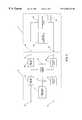
- FIG. 1is a block diagram of a line protector according to an embodiment of the present invention connected to a communications circuit;
- FIG. 2is an electrical schematic of the line protector of FIG. 1;
- FIG. 3is a perspective view of a line protector according to an embodiment of the present invention with the cover removed.
- FIG. 1shows an embodiment of a line protector according to the present invention connected to a communications circuit to be protected.
- line protector 10is connected to a communications circuit 20 which is to be protected.
- Line protector 10receives a first line input terminal 30 , such as a tip line of a telephone service wire pair, and a second line input terminal 32 , such as a ring line of the telephone service wire pair.
- First line input terminal 30 and second line input terminal 32are typically provided for telephone service as a twisted pair wire input from the telephone communications network.
- the overvoltage arrestor 34is connected between the first line input terminal 30 and the second input line input terminal 32 by device terminals (electrodes) and further includes a terminal (electrode) connected to a line protector ground 36 .
- the overvoltage arrestor 34may be provided as a gas discharge tube or as a transient voltage suppressor thyristor.
- the overvoltage arrestor 34is provided to clamp transient voltages that appear across the tip 30 and ring line 32 with respect to the line protector ground 36 .
- An example of a three electrode (terminal) gas discharge tube device suitable for use with the present inventionis the MiniTrigard® 2036 rated for 230 volts direct current (VDC) breakdown voltage manufactured by Joslyn Electronics Systems.
- line protector 10includes an isolation circuit 38 on the first line input terminal 30 and a corresponding isolation circuit 38 ′ on the second line input terminal 32 .
- the isolation circuits 38 , 38 ′help to provide isolation between the overvoltage arrestor 34 and the voltage clamping device circuit 40 to support hybrid overvoltage and overcurrent protection operations which coordinate the relative advantages and disadvantages of the different types of protection devices used for the overvoltage arrestor 34 and voltage clamping device circuit 40 .
- isolation circuits 38 , 38 ′may include temperature responsive current protection devices or inductor devices.
- the voltage clamping device circuit 40may include voltage clamping devices providing protection between each of the line input terminals 30 , 32 and the line protector ground 36 and may further include additional protection clamping differential voltages across the line input terminals 30 , 32 .
- Suitable devices for use as voltage clamping devicesinclude solid state semiconductor devices such as diodes or avalanche diodes. Alternatively, non-linear resistors may be employed such as zinc oxide, silicone carbide or other varistor materials.
- Suitable clamping devicesinclude bi-directional clamping diodes, for example, as sold under the tradename TransZorbTM.
- a preferred voltage clamping devicemay depend upon the line voltages in use in the communications circuit to be protected and include a P6KE24CA device available from General Semiconductor Company.
- the line protector 10 illustrated in FIG. 1further includes isolation circuits 48 , 48 ′ positioned between the voltage clamping device circuit 40 and the overvoltage arrestor 34 and the communications circuit 20 .
- Tip line output terminal 42 and ring line output terminal 46provide the overvoltage and overcurrent protected tip and ring signal from line protector 10 to corresponding to tip line input terminal 60 and ring line input terminal 62 of communications circuit 20 .
- the communications circuit deviceincludes a voltage clamping device 64 positioned across the differential voltage input from line input terminals 60 , 62 as well as additional telecommunications circuitry 66 . Also shown in the communications circuit 20 is the circuit ground 68 . Typically, in telephone communications line application environments there is at least some degree of distance or isolation between the line protector ground 36 and the communications circuit ground 68 which may, for example, result in a ground potential difference between line protector ground 36 and communications circuit ground 68 . Accordingly, the separate ground symbols are used to indicate that there may be a potential difference under certain transient operating conditions between the two grounds.
- FIG. 2an embodiment 100 of the line protector 10 of FIG. 1 is illustrated as an electrical schematic.
- the 230 volt gas discharge tube 134corresponds to the overvoltage arrestor 34 of FIG. 1 .
- the isolation circuits 138 , 138 ′ in the embodiment of FIG. 2each include a temperature responsive current protection device 152 , 152 ′ connected by one terminal to the tip input line terminal 30 and ring input line terminal 32 respectively. Fuses may also be provided on each input line.
- the temperature responsive current protection devices 152 , 152 ′are positive temperature coefficient resistor (PTC resistor) devices.
- PTC resistorpositive temperature coefficient resistor
- Suitable devices for use with the present invention as temperature responsive current protection devicesinclude devices such as ceramic or polymeric PTC devices, preferably polymeric devices, for example, devices available from Raychem Corporation under the registered trademark POLYSWITCHTM.
- a TR-250 model POLYSWITCHTMis utilized for the devices 152 , 152 ′.
- the isolation circuits 138 , 138 ′ in the embodiment of FIG. 2further include inductor devices 154 , 154 ′ connected between a second terminal of the positive temperature coefficient resistors 152 , 152 ′ and the voltage clamping devices of voltage clamping device circuit 140 .
- the inductor deviceshave an inductance value of 10 ⁇ H.
- the electrical schematic of FIG. 2shows both line to ground voltage clamping devices and a differential clamping device as being included in the voltage clamping device circuit 140 .
- the voltage clamping devices 156 , 158 , 160 in the schematic of FIG. 2are 24 volt TVS diodes available from General Semiconductor Company.
- Diode 156has a first terminal connected to the positive temperature coefficient resistor 152 through the inductor device 154 .
- the diode 156has a first terminal which is directly connected to the inductor 154 with no intervening capacitor in the circuit.
- Diode 158is similarly connected to the positive temperature coefficient resistor 152 ′ through inductor 154 ′ with a direct connection to inductor 154 ′ without an intervening capacitor.
- Both diode 156 and diode 158have a second terminal which is connected to the line protector ground 36 .
- Diodes 156 and 158are preferably selected to have a clamping voltage which clamps at a voltage level below that at which gas discharge tube 134 triggers and for their fast response capability allowing clamping of voltage by the diodes 156 , 158 during fast rising transient overvoltage events before the gas discharge tube 134 switches flow current in response to the overvoltage event. It is desirable, however, to provide sufficient voltage differential across gas discharge tube 134 to insure the gas discharge tube will trigger so as to ground the overvoltage event shortly after current begins to flow through diode 156 or diode 158 .
- the first and second positive temperature coefficient resistors 152 , 152 ′ and the first and second inductor devices 154 , 154 ′are selected so as to maintain a voltage across the gas discharge tube 134 sufficient to trigger the gas discharge tube 134 when the first and second diode 156 , 158 are triggered, for example, by an A/C power line overcurrent event or a lightning event.
- tip and ring lines 30 , 32are typically provided as a twisted wire pair, under normal conditions, overvoltage events either from A/C power line faults or lightning events are typically carried concurrently on both lines and, therefore, do not induce a differential voltage increase across the tip and ring lines 30 , 32 .
- the communications circuit 20typically includes components which are particularly sensitive to such differential voltage signals as they may operate responsive to differential signals input at low level voltages, typically well below 10 volts. Accordingly, even a relatively small differential voltage signal induced by a lightning strike or other line failure event can be problematic.
- Such a differential voltage spike conditionmay result due to variability in the characteristics of the protection devices, in particular, in the gas discharge tube 134 . More specifically, the gas discharge tube 134 may not be perfectly uniform side to side in its manufacture. Therefore, one side of the gas discharge tube 134 may trigger and bring the respective tip line 30 or ring line 32 to the level of the line protector ground 36 before the other of the tip line 30 or the ring line 32 is brought to this ground voltage level. Under such conditions, for a transient period of time, an unacceptably high differential voltage may be presented at the output line terminals 42 , 46 , thereby exposing communications circuit 20 to a high differential voltage input.
- an additional diode 160is provided in voltage clamping device circuit 140 which has a first terminal connected through the inductor device 154 to the positive temperature coefficient resistor 152 and a second terminal on the ring line 32 connected through the inductor device 154 ′ to the positive temperature coefficient resistor 152 ′.
- Diode 160thereby operates as a voltage clamp which may prevent large differential voltage signals from being passed through the line protector 10 to the communications circuit 20 .
- the circuit in FIG. 2further includes positive temperature coefficient resistors 148 , 150 .
- the positive temperature coefficient resistors 148 , 150connect the output side 42 , 46 of the overvoltage protection circuit components 134 , 138 , 138 ′, 140 to the communications circuit 20 and limit current flow from the overvoltage protection circuit elements to the voltage clamping device 64 of the communications circuit 20 .
- Such a current flowmay be generated when a ground potential difference is present between the line protector ground 36 and the circuit ground 68 .
- positive temperature coefficient resistors 148 , 150further serve to provide some isolation between voltage clamping device 64 and the line protector 100 to allow matching of the clamping voltage device 64 to facilitate operations of the line protector 100 when current is flowing through voltage clamping device 64 by maintaining a differential additional voltage across the overvoltage protection circuitry of line protector 100 above the clamping voltage of voltage clamping device 64 .
- Such current flow conditionsmay occur both from the ground potential different circumstance as described previously and can further occur when a fault condition imposes an undesired voltage input on the line protector ground 36 rather than tip or ring line 30 , 32 (i.e., a line protector ground fault event).
- the diodes 156 , 158may operate by clamping voltage in a manner which induces current flow in the reverse direction which, in turn, may cause the current to flow through towards tip and ring output line terminals 42 , 46 and the downstream communications circuit 20 .
- the impact of their nominal, off-state resistanceshould be considered to avoid degradation of signals. If their effective off-state resistance is too high (in combination with any DC resistance of the inductors 154 , 154 ′), then the insertion loss of the protection circuit could attenuate the signalling and/or powering from tip line 30 and ring line 32 sufficiently to interfere with normal operation of communications circuits 20 , such as private branch exchange (PBX) telephone sets.
- PBXprivate branch exchange
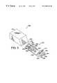
- line protector module 200includes a circuit device 210 and a housing cover 212 .
- the circuit device 210includes a circuit board 216 on which electrical components are mounted and an end plate 214 .
- the end plate 214is configured to mate with the housing cover 212 to form a protective housing around the circuit board 216 and the electrical components mounted to the circuit board 216 .
- the plate 214further includes the input and output pins of the line protector module 200 including the tip and ring line input terminals 230 , 232 , the line protector ground terminal 236 and the tip and ring line output terminals 242 , 246 .
- FIG. 3Various of the electrical component devices described previously in connection with FIG. 2 are shown in FIG. 3 with related numbers.
- a gas discharge tube 234 and diodes 256 , 258 and 260are illustrated.
- the positive temperature coefficient resistors 252 , 252 ′are interspersed and mounted adjacent the diodes 256 , 258 and 260 . This close adjacent proximity facilitates thermal transfer between the diodes 256 , 258 , 260 and the positive temperature coefficient resistors 252 , 252 ′.
- the thermally conductive adhesive material 270further thermally couples the positive temperature coefficient resistors 252 , 252 ′ to the diodes 256 , 258 , 260 .
- Both the adjacent placement and layout of the circuitry as well as the use of the thermally conductive adhesiveprovide thermal coupling between one or more of the voltage clamping devices 256 , 258 , 260 and one or more of the positive temperature coefficient resistors 252 , 252 ′ so as to reduce the likelihood that the positive temperature coefficient resistors 252 , 252 ′ will react too slowly to protect the diodes 256 , 258 , 260 from damage by heat generated in the diodes when they conduct current.
- Thisis particularly advantageous in that it may allow the use of smaller diode devices thereby allowing smaller packaging size for the line protector 200 .
- This smaller size capabilityresults from the fact that diodes with higher current ratings typically are provided in larger packages as the larger package size creates a greater thermal mass allowing more energy absorption before break down and damage to the materials of the diodes causing device failures.
- the placement of components to support thermal conduction as shown in FIG. 3also may be applied to the additional positive temperature coefficient resistors 148 , 150 illustrated in the embodiment of FIG. 2 .
- the diodes 156 , 158may be mounted adjacent to the positive temperature coefficient resistors 148 , 150 , respectively, and thermally coupled by thermally conductive adhesive. As described with reference to FIG. 3, this may provide an additional protection performance advantage by promoting faster trip time whereby the positive temperature coefficient resistors 148 , 150 respond to heating which occurs in the diodes 156 , 158 during ground potential difference current flow into the protected equipment.
- An additional performance advantage of the embodiment as illustrated in FIG. 2, which includes a direct connection between the inductor device 154 and the diode 156 and similarly the inductor device 154 ′ and the diode 158 ,is the better matching capability for protecting communications equipment 20 through faster response time and through eliminating a DC voltage offset between the diodes 156 , 158 and the communications equipment 20 which may be present in prior art devices such as that in U.S. Pat. No. 4,758,920.
- this approach without the use of the capacitormay be beneficially utilized even in telephone communication systems where the tip and ring lines 30 , 32 carry both the communications signal and a DC component which provides a power source to various circuitry which may be contained in the communications circuit 20 .
- DC power voltage levelsbetween about 12 volts and about 48 volts.
- the use of a circuit with and a direct connection between the inductors 154 , 154 ′ and the diodes 156 , 158may be limited in the ranges of DC power voltages which are suitable for use with the line protector as the diode clamping voltages typically are selected below the DC power voltage. Accordingly, for example, in the embodiment of FIG. 2 where 24 volt diodes are provided, the DC power voltage level for the application is preferably less than 24 volts and, more preferably, no more than 20 volts.
Landscapes
- Engineering & Computer Science (AREA)
- Signal Processing (AREA)
- Emergency Protection Circuit Devices (AREA)
Abstract
Description
Claims (13)
Priority Applications (7)
| Application Number | Priority Date | Filing Date | Title |
|---|---|---|---|
| US09/345,060US6266223B1 (en) | 1999-06-30 | 1999-06-30 | Line protector for a communications circuit |
| AU58989/00AAU5898900A (en) | 1999-06-30 | 2000-06-28 | Line protector for a communications circuit |
| CA002377456ACA2377456A1 (en) | 1999-06-30 | 2000-06-28 | Line protector for a communications circuit |
| PCT/US2000/017890WO2001001539A1 (en) | 1999-06-30 | 2000-06-28 | Line protector for a communications circuit |
| MXPA01013217AMXPA01013217A (en) | 1999-06-30 | 2000-06-28 | Line protector for a communications circuit. |
| EP00944984AEP1192696A1 (en) | 1999-06-30 | 2000-06-28 | Line protector for a communications circuit |
| BR0012458-3ABR0012458A (en) | 1999-06-30 | 2000-06-28 | Line protector for a communications circuit |
Applications Claiming Priority (1)
| Application Number | Priority Date | Filing Date | Title |
|---|---|---|---|
| US09/345,060US6266223B1 (en) | 1999-06-30 | 1999-06-30 | Line protector for a communications circuit |
Related Parent Applications (1)
| Application Number | Title | Priority Date | Filing Date |
|---|---|---|---|
| US08/870,118Continuation-In-PartUS5947452A (en) | 1996-06-10 | 1997-06-05 | Energy absorbing crash cushion |
Related Child Applications (1)
| Application Number | Title | Priority Date | Filing Date |
|---|---|---|---|
| US09/832,162DivisionUS6536985B2 (en) | 1997-06-05 | 2001-04-09 | Energy absorbing system for fixed roadside hazards |
Publications (1)
| Publication Number | Publication Date |
|---|---|
| US6266223B1true US6266223B1 (en) | 2001-07-24 |
Family
ID=23353315
Family Applications (1)
| Application Number | Title | Priority Date | Filing Date |
|---|---|---|---|
| US09/345,060Expired - LifetimeUS6266223B1 (en) | 1999-06-30 | 1999-06-30 | Line protector for a communications circuit |
Country Status (7)
| Country | Link |
|---|---|
| US (1) | US6266223B1 (en) |
| EP (1) | EP1192696A1 (en) |
| AU (1) | AU5898900A (en) |
| BR (1) | BR0012458A (en) |
| CA (1) | CA2377456A1 (en) |
| MX (1) | MXPA01013217A (en) |
| WO (1) | WO2001001539A1 (en) |
Cited By (25)
| Publication number | Priority date | Publication date | Assignee | Title |
|---|---|---|---|---|
| US20020080545A1 (en)* | 2000-12-26 | 2002-06-27 | Slater Byron J. | Excessive surge protection method and apparatus |
| US20050073793A1 (en)* | 2003-10-03 | 2005-04-07 | Mohammad Masghati | Dual stage current limiting surge protector system |
| US20050099755A1 (en)* | 2003-11-10 | 2005-05-12 | David Martin | Broadband surge protector with non-resetting current limiter |
| US20050152080A1 (en)* | 2003-08-21 | 2005-07-14 | Fultec Semiconductor Inc. | Integrated electronic disconnecting circuits, methods, and systems |
| US20050180080A1 (en)* | 2002-07-02 | 2005-08-18 | Fultec Semiconductor, Inc. | Protection and indication apparatus |
| US6982859B1 (en)* | 2000-03-24 | 2006-01-03 | Littelfuse, Inc. | Integrated overcurrent and overvoltage apparatus for use in the protection of telecommunication circuits |
| US20070070570A1 (en)* | 2005-09-26 | 2007-03-29 | Turner Donald B | Surge protection methods and apparatus |
| US20080204963A1 (en)* | 2007-02-28 | 2008-08-28 | Baker Scott K | Overvoltage protection plug |
| US20090108980A1 (en)* | 2007-10-09 | 2009-04-30 | Littelfuse, Inc. | Fuse providing overcurrent and thermal protection |
| USD591691S1 (en) | 2007-02-28 | 2009-05-05 | Adc Telecommunications, Inc. | Overvoltage protection plug |
| US20090269954A1 (en)* | 2008-04-25 | 2009-10-29 | Vern Loch | Circuit protection block |
| US20100182727A1 (en)* | 2009-01-16 | 2010-07-22 | Circa Enterprises, Inc. | Surge protection module |
| USD620896S1 (en) | 2008-05-27 | 2010-08-03 | Adc Telecommunications, Inc. | Overvoltage protection plug |
| US20110058286A1 (en)* | 2009-09-09 | 2011-03-10 | Denso Wave Incorporated | Electrical apparatus with higher durability against surges |
| US20120026639A1 (en)* | 2010-07-27 | 2012-02-02 | Regal Beloit Corporation | Methods and systems for transient voltage protection |
| US8395875B2 (en) | 2010-08-13 | 2013-03-12 | Andrew F. Tresness | Spark gap apparatus |
| US20130063845A1 (en)* | 2011-09-08 | 2013-03-14 | Phoenix Contact Gmbh & Co. Kg | Overvoltage protection equipment |
| US8411404B2 (en) | 2008-05-27 | 2013-04-02 | Adc Telecommunications, Inc. | Overvoltage protection plug |
| US20150280428A1 (en)* | 2014-03-25 | 2015-10-01 | Adtran Inc. | Gas tube impulse protection |
| US20150326006A1 (en)* | 2012-06-28 | 2015-11-12 | Zte Corporation | Protection circuit of communication interface |
| US20160097803A1 (en)* | 2014-10-01 | 2016-04-07 | Hamilton Sundstrand Corporation | Built in test circuit for transient voltage suppressor devices |
| US20160308347A1 (en)* | 2015-04-16 | 2016-10-20 | NLightning Technology Ltd. | Protection module and decoupling component thereof for symmetrical twisted pairs |
| US9735725B2 (en) | 2014-01-21 | 2017-08-15 | Regal Beloit America, Inc. | Methods and systems for transient voltage protection |
| US20180301897A1 (en)* | 2017-04-17 | 2018-10-18 | Comtest Networks Inc. | Modular access connection system |
| CN110635464A (en)* | 2019-10-16 | 2019-12-31 | 李吉晓 | Common-mode lightning protection circuit of LED lighting lamp |
Families Citing this family (7)
| Publication number | Priority date | Publication date | Assignee | Title |
|---|---|---|---|---|
| AU2002951888A0 (en)* | 2002-10-08 | 2002-10-24 | Fultec Pty Ltd | A protection device for preventing the flow of undersirable transients |
| US7342433B2 (en) | 2004-11-09 | 2008-03-11 | Fultec Semiconductor, Inc. | Apparatus and method for enhanced transient blocking |
| WO2006053314A2 (en) | 2004-11-09 | 2006-05-18 | Fultec Semiconductor, Inc. | Apparatus and method for high-voltage transient blocking using low-voltage elements |
| US7369387B2 (en) | 2004-11-09 | 2008-05-06 | Fultec Semiconductor, Inc. | Apparatus and method for temperature-dependent transient blocking |
| US7492566B2 (en) | 2005-01-14 | 2009-02-17 | Bourns, Inc. | Low resistance transient blocking unit |
| US7576962B2 (en) | 2005-06-16 | 2009-08-18 | Bourns, Inc. | Transient blocking apparatus with reset |
| DE202014100428U1 (en)* | 2014-01-31 | 2014-02-12 | Epcos Ag | Circuit arrangement for overvoltage protection |
Citations (28)
| Publication number | Priority date | Publication date | Assignee | Title |
|---|---|---|---|---|
| DE1513038A1 (en) | 1965-09-29 | 1969-07-10 | Siemens Ag | Circuit arrangement for reducing signal distortions caused by overvoltage protection circuits |
| US3571658A (en) | 1968-11-22 | 1971-03-23 | Micafil Ag | Protective system for capacitive voltage transformers including a circuit for t{d fh-coupling |
| US3725613A (en) | 1971-02-25 | 1973-04-03 | Rochester Tel Corp | Apparatus for protecting and testing telephone network |
| DE2334698A1 (en) | 1972-02-20 | 1975-01-23 | Sankosha Co Ltd | OVERVOLTAGE PROTECTION |
| US3944753A (en) | 1974-10-31 | 1976-03-16 | Proctor & Associates Company | Apparatus for distinguishing voice and other noise signals from legitimate multi-frequency tone signals present on telephone or similar communication lines |
| US3950676A (en) | 1973-01-11 | 1976-04-13 | Felten & Guilleaume Carlswerk Aktiengesellschaft | Transmission line-communications equipment coupling unit having short-circuit and overvoltage protection |
| US4039763A (en) | 1976-07-28 | 1977-08-02 | Bell Telephone Laboratories, Incorporated | Key telephone communication path interface |
| US4203006A (en) | 1978-04-20 | 1980-05-13 | Prentice Corporation | Direct access coupler |
| US4254442A (en) | 1976-12-20 | 1981-03-03 | U.S. Philips Corporation | Circuit for the protection of telephone lines |
| US4254447A (en) | 1979-04-10 | 1981-03-03 | Rca Corporation | Integrated circuit heat dissipator |
| FR2504323A1 (en) | 1981-04-16 | 1982-10-22 | Radiotechnique Compelec | SUBSCRIBER TELEPHONE STATION PROVIDED WITH AN OVERVOLTAGE PROTECTION DEVICE |
| US4455586A (en) | 1980-10-24 | 1984-06-19 | Oneac Corporation | High voltage filtering and protection circuit |
| US4536618A (en) | 1983-10-14 | 1985-08-20 | Novation, Inc. | Telephone line interface |
| US4544983A (en) | 1983-04-28 | 1985-10-01 | Northern Telecom Limited | Overvoltage protection device |
| US4586104A (en) | 1983-12-12 | 1986-04-29 | Rit Research Corp. | Passive overvoltage protection devices, especially for protection of computer equipment connected to data lines |
| US4591666A (en) | 1983-12-05 | 1986-05-27 | Gte Business Communication Systems Inc. | Protection circuitry for subscriber's telephone circuit equipped with repertory memory |
| EP0186873A2 (en) | 1984-12-24 | 1986-07-09 | Nippon Telegraph And Telephone Corporation | Protector circuit |
| GB2172453A (en) | 1985-03-11 | 1986-09-17 | Dubilier Beswick Div | Overvoltage protection arrangements |
| US4628398A (en) | 1981-03-02 | 1986-12-09 | The M-O Valve Company Limited | Surge voltage protection arrangements |
| US4758920A (en) | 1987-03-02 | 1988-07-19 | Oneac Corporation | Telephone and data overvoltage protection apparatus |
| EP0327359A1 (en) | 1988-02-03 | 1989-08-09 | BRITISH TELECOMMUNICATIONS public limited company | Protector device |
| US4866563A (en) | 1987-09-24 | 1989-09-12 | Semitron Cricklade, Ltd. | Transient suppressor device assembly |
| US4907120A (en) | 1988-12-08 | 1990-03-06 | Reliance Comm/Tec Corporation | Line protector for a communications circuit |
| WO1992006523A1 (en) | 1990-09-28 | 1992-04-16 | Raychem Limited | Circuit protection device |
| GB2267789A (en) | 1992-06-08 | 1993-12-15 | Oneac Corp | Telephone line overvoltage protection |
| US5379176A (en) | 1993-05-03 | 1995-01-03 | John Fluke Mfg. Co., Inc. | Protective input circuit for an instrument |
| US5721663A (en) | 1995-01-17 | 1998-02-24 | Tii Industries, Inc. | Overvoltage protection modules with back-up protection for communication lines |
| DE19708802A1 (en) | 1997-03-05 | 1998-10-15 | Krone Ag | Electrical circuit with voltage and current limiting devices |
Family Cites Families (1)
| Publication number | Priority date | Publication date | Assignee | Title |
|---|---|---|---|---|
| DE3340927A1 (en)* | 1983-11-11 | 1985-05-23 | Siemens AG, 1000 Berlin und 8000 München | CIRCUIT ARRANGEMENT FOR DERIVATING OVERVOLTAGE |
- 1999
- 1999-06-30USUS09/345,060patent/US6266223B1/ennot_activeExpired - Lifetime
- 2000
- 2000-06-28MXMXPA01013217Apatent/MXPA01013217A/enunknown
- 2000-06-28CACA002377456Apatent/CA2377456A1/ennot_activeAbandoned
- 2000-06-28AUAU58989/00Apatent/AU5898900A/ennot_activeAbandoned
- 2000-06-28EPEP00944984Apatent/EP1192696A1/ennot_activeWithdrawn
- 2000-06-28BRBR0012458-3Apatent/BR0012458A/ennot_activeApplication Discontinuation
- 2000-06-28WOPCT/US2000/017890patent/WO2001001539A1/enactiveApplication Filing
Patent Citations (31)
| Publication number | Priority date | Publication date | Assignee | Title |
|---|---|---|---|---|
| DE1513038A1 (en) | 1965-09-29 | 1969-07-10 | Siemens Ag | Circuit arrangement for reducing signal distortions caused by overvoltage protection circuits |
| US3571658A (en) | 1968-11-22 | 1971-03-23 | Micafil Ag | Protective system for capacitive voltage transformers including a circuit for t{d fh-coupling |
| US3725613A (en) | 1971-02-25 | 1973-04-03 | Rochester Tel Corp | Apparatus for protecting and testing telephone network |
| DE2334698A1 (en) | 1972-02-20 | 1975-01-23 | Sankosha Co Ltd | OVERVOLTAGE PROTECTION |
| US3950676A (en) | 1973-01-11 | 1976-04-13 | Felten & Guilleaume Carlswerk Aktiengesellschaft | Transmission line-communications equipment coupling unit having short-circuit and overvoltage protection |
| US3944753A (en) | 1974-10-31 | 1976-03-16 | Proctor & Associates Company | Apparatus for distinguishing voice and other noise signals from legitimate multi-frequency tone signals present on telephone or similar communication lines |
| US4039763A (en) | 1976-07-28 | 1977-08-02 | Bell Telephone Laboratories, Incorporated | Key telephone communication path interface |
| US4254442A (en) | 1976-12-20 | 1981-03-03 | U.S. Philips Corporation | Circuit for the protection of telephone lines |
| US4203006A (en) | 1978-04-20 | 1980-05-13 | Prentice Corporation | Direct access coupler |
| US4254447A (en) | 1979-04-10 | 1981-03-03 | Rca Corporation | Integrated circuit heat dissipator |
| US4455586A (en) | 1980-10-24 | 1984-06-19 | Oneac Corporation | High voltage filtering and protection circuit |
| US4628398A (en) | 1981-03-02 | 1986-12-09 | The M-O Valve Company Limited | Surge voltage protection arrangements |
| FR2504323A1 (en) | 1981-04-16 | 1982-10-22 | Radiotechnique Compelec | SUBSCRIBER TELEPHONE STATION PROVIDED WITH AN OVERVOLTAGE PROTECTION DEVICE |
| US4544983A (en) | 1983-04-28 | 1985-10-01 | Northern Telecom Limited | Overvoltage protection device |
| US4536618A (en) | 1983-10-14 | 1985-08-20 | Novation, Inc. | Telephone line interface |
| US4591666A (en) | 1983-12-05 | 1986-05-27 | Gte Business Communication Systems Inc. | Protection circuitry for subscriber's telephone circuit equipped with repertory memory |
| US4586104A (en) | 1983-12-12 | 1986-04-29 | Rit Research Corp. | Passive overvoltage protection devices, especially for protection of computer equipment connected to data lines |
| EP0186873A2 (en) | 1984-12-24 | 1986-07-09 | Nippon Telegraph And Telephone Corporation | Protector circuit |
| GB2172453A (en) | 1985-03-11 | 1986-09-17 | Dubilier Beswick Div | Overvoltage protection arrangements |
| US4758920A (en) | 1987-03-02 | 1988-07-19 | Oneac Corporation | Telephone and data overvoltage protection apparatus |
| EP0338107A1 (en) | 1987-03-02 | 1989-10-25 | Oneac Corporation | Overvoltage protection circuit used with a pair of telephone lines or similar data communication channels |
| US4866563A (en) | 1987-09-24 | 1989-09-12 | Semitron Cricklade, Ltd. | Transient suppressor device assembly |
| EP0327359A1 (en) | 1988-02-03 | 1989-08-09 | BRITISH TELECOMMUNICATIONS public limited company | Protector device |
| US4907120A (en) | 1988-12-08 | 1990-03-06 | Reliance Comm/Tec Corporation | Line protector for a communications circuit |
| WO1992006523A1 (en) | 1990-09-28 | 1992-04-16 | Raychem Limited | Circuit protection device |
| US5416663A (en) | 1990-09-28 | 1995-05-16 | Raychem Limited | Arrangement for protecting telecommunications equipment from voltage transients |
| US5513059A (en) | 1990-09-28 | 1996-04-30 | Raychem Limited | Arrangement for protecting telecommunications equipment from voltage transients |
| GB2267789A (en) | 1992-06-08 | 1993-12-15 | Oneac Corp | Telephone line overvoltage protection |
| US5379176A (en) | 1993-05-03 | 1995-01-03 | John Fluke Mfg. Co., Inc. | Protective input circuit for an instrument |
| US5721663A (en) | 1995-01-17 | 1998-02-24 | Tii Industries, Inc. | Overvoltage protection modules with back-up protection for communication lines |
| DE19708802A1 (en) | 1997-03-05 | 1998-10-15 | Krone Ag | Electrical circuit with voltage and current limiting devices |
Cited By (43)
| Publication number | Priority date | Publication date | Assignee | Title |
|---|---|---|---|---|
| US6982859B1 (en)* | 2000-03-24 | 2006-01-03 | Littelfuse, Inc. | Integrated overcurrent and overvoltage apparatus for use in the protection of telecommunication circuits |
| US7561399B2 (en) | 2000-12-26 | 2009-07-14 | Landis+Gyr, Inc. | Excessive surge protection method and apparatus |
| US20060126255A1 (en)* | 2000-12-26 | 2006-06-15 | Landisinc. | Excessive surge protection method and apparatus |
| US20020080545A1 (en)* | 2000-12-26 | 2002-06-27 | Slater Byron J. | Excessive surge protection method and apparatus |
| US7616420B2 (en)* | 2000-12-26 | 2009-11-10 | Landis+Gyr, Inc. | Excessive surge protection method and apparatus |
| US20050180080A1 (en)* | 2002-07-02 | 2005-08-18 | Fultec Semiconductor, Inc. | Protection and indication apparatus |
| US7457093B2 (en) | 2002-07-02 | 2008-11-25 | Fultec Semiconductor, Inc. | Protection and indication apparatus |
| US20050152080A1 (en)* | 2003-08-21 | 2005-07-14 | Fultec Semiconductor Inc. | Integrated electronic disconnecting circuits, methods, and systems |
| US7262946B2 (en)* | 2003-08-21 | 2007-08-28 | Fultec Semiconductor, Inc. | Integrated electronic disconnecting circuits, methods, and systems |
| US20050073793A1 (en)* | 2003-10-03 | 2005-04-07 | Mohammad Masghati | Dual stage current limiting surge protector system |
| US6992874B2 (en)* | 2003-10-03 | 2006-01-31 | Illinois Tool Works Inc. | Dual stage current limiting surge protector system |
| US20050099755A1 (en)* | 2003-11-10 | 2005-05-12 | David Martin | Broadband surge protector with non-resetting current limiter |
| US20070070570A1 (en)* | 2005-09-26 | 2007-03-29 | Turner Donald B | Surge protection methods and apparatus |
| USD591691S1 (en) | 2007-02-28 | 2009-05-05 | Adc Telecommunications, Inc. | Overvoltage protection plug |
| US9865995B2 (en) | 2007-02-28 | 2018-01-09 | Commscope Technologies Llc | Overvoltage protection plug |
| US20080204963A1 (en)* | 2007-02-28 | 2008-08-28 | Baker Scott K | Overvoltage protection plug |
| US8064182B2 (en) | 2007-02-28 | 2011-11-22 | Adc Telecommunications, Inc. | Overvoltage protection plug |
| US20090108980A1 (en)* | 2007-10-09 | 2009-04-30 | Littelfuse, Inc. | Fuse providing overcurrent and thermal protection |
| US7946863B2 (en) | 2008-04-25 | 2011-05-24 | Adc Telecommunications, Inc. | Circuit protection block |
| US20090269954A1 (en)* | 2008-04-25 | 2009-10-29 | Vern Loch | Circuit protection block |
| USD620896S1 (en) | 2008-05-27 | 2010-08-03 | Adc Telecommunications, Inc. | Overvoltage protection plug |
| US8411404B2 (en) | 2008-05-27 | 2013-04-02 | Adc Telecommunications, Inc. | Overvoltage protection plug |
| US20100182727A1 (en)* | 2009-01-16 | 2010-07-22 | Circa Enterprises, Inc. | Surge protection module |
| US8320094B2 (en)* | 2009-01-16 | 2012-11-27 | Circa Enterprises, Inc. | Surge protection module |
| US20110058286A1 (en)* | 2009-09-09 | 2011-03-10 | Denso Wave Incorporated | Electrical apparatus with higher durability against surges |
| US8786992B2 (en)* | 2009-09-09 | 2014-07-22 | Denso Wave Incorporated | Electrical apparatus with higher durability against surges |
| US20120026639A1 (en)* | 2010-07-27 | 2012-02-02 | Regal Beloit Corporation | Methods and systems for transient voltage protection |
| US8520355B2 (en)* | 2010-07-27 | 2013-08-27 | Regal Beloit America, Inc. | Methods and systems for transient voltage protection |
| US8395875B2 (en) | 2010-08-13 | 2013-03-12 | Andrew F. Tresness | Spark gap apparatus |
| US20130063845A1 (en)* | 2011-09-08 | 2013-03-14 | Phoenix Contact Gmbh & Co. Kg | Overvoltage protection equipment |
| US8982525B2 (en)* | 2011-09-08 | 2015-03-17 | Phoenix Contact Gmbh & Co. Kg | Overvoltage protection equipment |
| US20150326006A1 (en)* | 2012-06-28 | 2015-11-12 | Zte Corporation | Protection circuit of communication interface |
| US9496705B2 (en)* | 2012-06-28 | 2016-11-15 | Zte Corporation | Protection circuit of communication interface |
| US9735725B2 (en) | 2014-01-21 | 2017-08-15 | Regal Beloit America, Inc. | Methods and systems for transient voltage protection |
| US9548608B2 (en)* | 2014-03-25 | 2017-01-17 | Adtran, Inc. | Gas tube impulse protection |
| US20150280428A1 (en)* | 2014-03-25 | 2015-10-01 | Adtran Inc. | Gas tube impulse protection |
| US20160097803A1 (en)* | 2014-10-01 | 2016-04-07 | Hamilton Sundstrand Corporation | Built in test circuit for transient voltage suppressor devices |
| US9671453B2 (en)* | 2014-10-01 | 2017-06-06 | Hamilton Sundstrand Corporation | Built in test circuit for transient voltage suppressor devices |
| US20160308347A1 (en)* | 2015-04-16 | 2016-10-20 | NLightning Technology Ltd. | Protection module and decoupling component thereof for symmetrical twisted pairs |
| US10320968B2 (en)* | 2015-04-16 | 2019-06-11 | NLightning Technology Ltd. | Protection module and decoupling component thereof for symmetrical twisted pairs |
| US20180301897A1 (en)* | 2017-04-17 | 2018-10-18 | Comtest Networks Inc. | Modular access connection system |
| US10770890B2 (en)* | 2017-04-17 | 2020-09-08 | Comtest Networks Inc. | Modular access connection system |
| CN110635464A (en)* | 2019-10-16 | 2019-12-31 | 李吉晓 | Common-mode lightning protection circuit of LED lighting lamp |
Also Published As
| Publication number | Publication date |
|---|---|
| CA2377456A1 (en) | 2001-01-04 |
| AU5898900A (en) | 2001-01-31 |
| WO2001001539A1 (en) | 2001-01-04 |
| MXPA01013217A (en) | 2002-06-21 |
| BR0012458A (en) | 2002-04-02 |
| EP1192696A1 (en) | 2002-04-03 |
Similar Documents
| Publication | Publication Date | Title |
|---|---|---|
| US6266223B1 (en) | Line protector for a communications circuit | |
| EP0550554B1 (en) | Circuit protection device | |
| JP2005532022A (en) | Protection indication device | |
| US6298134B1 (en) | System for protecting telecommunications equipment from transient voltages | |
| CN113439372B (en) | Protection against AC voltage conditions | |
| US7106573B2 (en) | Protection circuit for a digital subscriber line device | |
| CN114097157B (en) | Surge protection device for protecting multiple direct-current or alternating-current power lines | |
| WO2006086564A2 (en) | Flexible secondary overcurrent protection | |
| WO2015021801A1 (en) | Surge protection device and method | |
| JP2002354662A (en) | Lightning protection circuit | |
| US6992874B2 (en) | Dual stage current limiting surge protector system | |
| US5721663A (en) | Overvoltage protection modules with back-up protection for communication lines | |
| JPH06217452A (en) | Protective circuit for communication | |
| JP3473819B2 (en) | Lightning protection adapter | |
| CN210404733U (en) | Alternating current power supply lightning protection device with overcurrent and overvoltage protection functions | |
| JPH07184319A (en) | Protective circuit | |
| JPH04304096A (en) | Subscriber-circuit protecting module apparatus | |
| JP2002223327A (en) | Safety device | |
| JPH02168815A (en) | Solid state station protector | |
| CN116826660A (en) | Surge protection circuit and system | |
| JPH03124220A (en) | Contact protective circuit | |
| JPS6188722A (en) | Protector for communication | |
| TH74368A (en) | Specific protection protocols applicable to specific telecommunication installations. And the protection cycle for the successful implementation of the methodology. | |
| TH25503B (en) | Specific protection protocols applicable to specific telecommunication installations. And the protection cycle for the successful implementation of the methodology. | |
| JPS63257416A (en) | Protective circuit of communication equipment |
Legal Events
| Date | Code | Title | Description |
|---|---|---|---|
| AS | Assignment | Owner name:RAYCHEM CORPORATION, CALIFORNIA Free format text:ASSIGNMENT OF ASSIGNORS INTEREST;ASSIGNOR:CURRY, WILLIAM J.;REEL/FRAME:010075/0863 Effective date:19990629 | |
| AS | Assignment | Owner name:TYCO INTERNATIONAL LTD., A CORPORATION OF BERMUDA, Free format text:MERGER & REORGANIZATION;ASSIGNOR:RAYCHEM CORPORATION, A CORPORATION OF DELAWARE;REEL/FRAME:011682/0001 Effective date:19990812 Owner name:AMP INCORPORATED, A CORPORATION OF PENNSYLVANIA, P Free format text:MERGER & REORGANIZATION;ASSIGNOR:RAYCHEM CORPORATION, A CORPORATION OF DELAWARE;REEL/FRAME:011682/0001 Effective date:19990812 Owner name:TYCO INTERNATIONAL (PA), INC., A CORPORATION OF NE Free format text:MERGER & REORGANIZATION;ASSIGNOR:RAYCHEM CORPORATION, A CORPORATION OF DELAWARE;REEL/FRAME:011682/0001 Effective date:19990812 | |
| AS | Assignment | Owner name:TYCO ELECTRONICS CORPORATION, A CORPORATION OF PEN Free format text:CHANGE OF NAME;ASSIGNOR:AMP INCORPORATED, A CORPORATION OF PENNSYLVANIA;REEL/FRAME:011675/0436 Effective date:19990913 | |
| STCF | Information on status: patent grant | Free format text:PATENTED CASE | |
| FEPP | Fee payment procedure | Free format text:PAYOR NUMBER ASSIGNED (ORIGINAL EVENT CODE: ASPN); ENTITY STATUS OF PATENT OWNER: LARGE ENTITY | |
| FPAY | Fee payment | Year of fee payment:4 | |
| FPAY | Fee payment | Year of fee payment:8 | |
| FPAY | Fee payment | Year of fee payment:12 | |
| AS | Assignment | Owner name:TYCO ELECTRONICS SERVICES GMBH, SWITZERLAND Free format text:ASSIGNMENT OF ASSIGNORS INTEREST;ASSIGNOR:TYCO ELECTRONICS CORPORATION;REEL/FRAME:036074/0740 Effective date:20150410 | |
| AS | Assignment | Owner name:COMMSCOPE EMEA LIMITED, IRELAND Free format text:ASSIGNMENT OF ASSIGNORS INTEREST;ASSIGNOR:TYCO ELECTRONICS SERVICES GMBH;REEL/FRAME:036956/0001 Effective date:20150828 | |
| AS | Assignment | Owner name:COMMSCOPE TECHNOLOGIES LLC, NORTH CAROLINA Free format text:ASSIGNMENT OF ASSIGNORS INTEREST;ASSIGNOR:COMMSCOPE EMEA LIMITED;REEL/FRAME:037012/0001 Effective date:20150828 | |
| AS | Assignment | Owner name:JPMORGAN CHASE BANK, N.A., AS COLLATERAL AGENT, ILLINOIS Free format text:PATENT SECURITY AGREEMENT (TERM);ASSIGNOR:COMMSCOPE TECHNOLOGIES LLC;REEL/FRAME:037513/0709 Effective date:20151220 Owner name:JPMORGAN CHASE BANK, N.A., AS COLLATERAL AGENT, ILLINOIS Free format text:PATENT SECURITY AGREEMENT (ABL);ASSIGNOR:COMMSCOPE TECHNOLOGIES LLC;REEL/FRAME:037514/0196 Effective date:20151220 Owner name:JPMORGAN CHASE BANK, N.A., AS COLLATERAL AGENT, IL Free format text:PATENT SECURITY AGREEMENT (TERM);ASSIGNOR:COMMSCOPE TECHNOLOGIES LLC;REEL/FRAME:037513/0709 Effective date:20151220 Owner name:JPMORGAN CHASE BANK, N.A., AS COLLATERAL AGENT, IL Free format text:PATENT SECURITY AGREEMENT (ABL);ASSIGNOR:COMMSCOPE TECHNOLOGIES LLC;REEL/FRAME:037514/0196 Effective date:20151220 | |
| AS | Assignment | Owner name:COMMSCOPE TECHNOLOGIES LLC, NORTH CAROLINA Free format text:RELEASE BY SECURED PARTY;ASSIGNOR:JPMORGAN CHASE BANK, N.A.;REEL/FRAME:048840/0001 Effective date:20190404 Owner name:REDWOOD SYSTEMS, INC., NORTH CAROLINA Free format text:RELEASE BY SECURED PARTY;ASSIGNOR:JPMORGAN CHASE BANK, N.A.;REEL/FRAME:048840/0001 Effective date:20190404 Owner name:ANDREW LLC, NORTH CAROLINA Free format text:RELEASE BY SECURED PARTY;ASSIGNOR:JPMORGAN CHASE BANK, N.A.;REEL/FRAME:048840/0001 Effective date:20190404 Owner name:ALLEN TELECOM LLC, ILLINOIS Free format text:RELEASE BY SECURED PARTY;ASSIGNOR:JPMORGAN CHASE BANK, N.A.;REEL/FRAME:048840/0001 Effective date:20190404 Owner name:COMMSCOPE, INC. OF NORTH CAROLINA, NORTH CAROLINA Free format text:RELEASE BY SECURED PARTY;ASSIGNOR:JPMORGAN CHASE BANK, N.A.;REEL/FRAME:048840/0001 Effective date:20190404 Owner name:COMMSCOPE, INC. OF NORTH CAROLINA, NORTH CAROLINA Free format text:RELEASE BY SECURED PARTY;ASSIGNOR:JPMORGAN CHASE BANK, N.A.;REEL/FRAME:049260/0001 Effective date:20190404 Owner name:ALLEN TELECOM LLC, ILLINOIS Free format text:RELEASE BY SECURED PARTY;ASSIGNOR:JPMORGAN CHASE BANK, N.A.;REEL/FRAME:049260/0001 Effective date:20190404 Owner name:COMMSCOPE TECHNOLOGIES LLC, NORTH CAROLINA Free format text:RELEASE BY SECURED PARTY;ASSIGNOR:JPMORGAN CHASE BANK, N.A.;REEL/FRAME:049260/0001 Effective date:20190404 Owner name:REDWOOD SYSTEMS, INC., NORTH CAROLINA Free format text:RELEASE BY SECURED PARTY;ASSIGNOR:JPMORGAN CHASE BANK, N.A.;REEL/FRAME:049260/0001 Effective date:20190404 Owner name:ANDREW LLC, NORTH CAROLINA Free format text:RELEASE BY SECURED PARTY;ASSIGNOR:JPMORGAN CHASE BANK, N.A.;REEL/FRAME:049260/0001 Effective date:20190404 | |
| AS | Assignment | Owner name:WILMINGTON TRUST, NATIONAL ASSOCIATION, AS COLLATE Free format text:PATENT SECURITY AGREEMENT;ASSIGNOR:COMMSCOPE TECHNOLOGIES LLC;REEL/FRAME:049892/0051 Effective date:20190404 Owner name:JPMORGAN CHASE BANK, N.A., NEW YORK Free format text:ABL SECURITY AGREEMENT;ASSIGNORS:COMMSCOPE, INC. OF NORTH CAROLINA;COMMSCOPE TECHNOLOGIES LLC;ARRIS ENTERPRISES LLC;AND OTHERS;REEL/FRAME:049892/0396 Effective date:20190404 Owner name:JPMORGAN CHASE BANK, N.A., NEW YORK Free format text:TERM LOAN SECURITY AGREEMENT;ASSIGNORS:COMMSCOPE, INC. OF NORTH CAROLINA;COMMSCOPE TECHNOLOGIES LLC;ARRIS ENTERPRISES LLC;AND OTHERS;REEL/FRAME:049905/0504 Effective date:20190404 Owner name:WILMINGTON TRUST, NATIONAL ASSOCIATION, AS COLLATERAL AGENT, CONNECTICUT Free format text:PATENT SECURITY AGREEMENT;ASSIGNOR:COMMSCOPE TECHNOLOGIES LLC;REEL/FRAME:049892/0051 Effective date:20190404 | |
| AS | Assignment | Owner name:RUCKUS WIRELESS, LLC (F/K/A RUCKUS WIRELESS, INC.), NORTH CAROLINA Free format text:RELEASE OF SECURITY INTEREST AT REEL/FRAME 049905/0504;ASSIGNOR:JPMORGAN CHASE BANK, N.A., AS COLLATERAL AGENT;REEL/FRAME:071477/0255 Effective date:20241217 Owner name:COMMSCOPE TECHNOLOGIES LLC, NORTH CAROLINA Free format text:RELEASE OF SECURITY INTEREST AT REEL/FRAME 049905/0504;ASSIGNOR:JPMORGAN CHASE BANK, N.A., AS COLLATERAL AGENT;REEL/FRAME:071477/0255 Effective date:20241217 Owner name:COMMSCOPE, INC. OF NORTH CAROLINA, NORTH CAROLINA Free format text:RELEASE OF SECURITY INTEREST AT REEL/FRAME 049905/0504;ASSIGNOR:JPMORGAN CHASE BANK, N.A., AS COLLATERAL AGENT;REEL/FRAME:071477/0255 Effective date:20241217 Owner name:ARRIS SOLUTIONS, INC., NORTH CAROLINA Free format text:RELEASE OF SECURITY INTEREST AT REEL/FRAME 049905/0504;ASSIGNOR:JPMORGAN CHASE BANK, N.A., AS COLLATERAL AGENT;REEL/FRAME:071477/0255 Effective date:20241217 Owner name:ARRIS TECHNOLOGY, INC., NORTH CAROLINA Free format text:RELEASE OF SECURITY INTEREST AT REEL/FRAME 049905/0504;ASSIGNOR:JPMORGAN CHASE BANK, N.A., AS COLLATERAL AGENT;REEL/FRAME:071477/0255 Effective date:20241217 Owner name:ARRIS ENTERPRISES LLC (F/K/A ARRIS ENTERPRISES, INC.), NORTH CAROLINA Free format text:RELEASE OF SECURITY INTEREST AT REEL/FRAME 049905/0504;ASSIGNOR:JPMORGAN CHASE BANK, N.A., AS COLLATERAL AGENT;REEL/FRAME:071477/0255 Effective date:20241217 |