US6266101B1 - Y/C separator - Google Patents
Y/C separatorDownload PDFInfo
- Publication number
- US6266101B1 US6266101B1US08/961,417US96141797AUS6266101B1US 6266101 B1US6266101 B1US 6266101B1US 96141797 AUS96141797 AUS 96141797AUS 6266101 B1US6266101 B1US 6266101B1
- Authority
- US
- United States
- Prior art keywords
- generating
- signal
- color
- luminance signal
- color signals
- Prior art date
- Legal status (The legal status is an assumption and is not a legal conclusion. Google has not performed a legal analysis and makes no representation as to the accuracy of the status listed.)
- Expired - Lifetime
Links
Images


Classifications
- H—ELECTRICITY
- H04—ELECTRIC COMMUNICATION TECHNIQUE
- H04N—PICTORIAL COMMUNICATION, e.g. TELEVISION
- H04N9/00—Details of colour television systems
- H04N9/77—Circuits for processing the brightness signal and the chrominance signal relative to each other, e.g. adjusting the phase of the brightness signal relative to the colour signal, correcting differential gain or differential phase
- H04N9/78—Circuits for processing the brightness signal and the chrominance signal relative to each other, e.g. adjusting the phase of the brightness signal relative to the colour signal, correcting differential gain or differential phase for separating the brightness signal or the chrominance signal from the colour television signal, e.g. using comb filter
Definitions
- the inventionrelates to the field of color image signal processing.
- the present inventionrelates to a Y/C separator which generates a luminance signal and a chrominance (color difference) signal of a sequential scanning system on the basis of an image signal of an interlaced scanning system, and to a camera comprising such a Y/C separator.
- a Y/C separation circuit(Y: Luminance signal, and C: Color difference signal) is used.
- the Y/C separation circuitincludes a circuit which simply generates a luminance signal and a color difference signal, and, additionally, for example, a circuit provided with a function which receives an image signal of an interlaced scanning system and generates a luminance signal and a color difference signal of a sequential scanning system.
- It is an object of the present inventionprovide a Y/C separator capable of avoiding distortion of an image and deterioration of the resolution in the vertical direction.
- the present inventionmakes substantially all scanning lines different in content from one another without repeating one scanning line. Due to this, distortion of an image and deterioration of the resolution in the vertical direction which have been generated in case of repeating each scanning line, can be avoided.
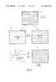
- FIG. 1is a diagram of a camera with a specific embodiment of the of Y/C separator in accordance with the invention
- FIGS. 2 a and 2 bare first diagrams for explaining the operation of a specific embodiment the invention.
- FIGS. 3 a and 3 bare second diagram for explaining the operation of a specific embodiment of the invention.
- FIG. 4is a schematic block diagram showing the conversion of an input interlaced signal into an output sequential signal.
- a Y/C separation circuit of the inventionhas an analog-to-digital converter (A/D) 3 linked to a CCD 2 for interlaced scanning, a luminance signal generating circuit (LSG) 4 , a color signal generating circuit (buffer; BUF) 5 , an arithmetic circuit (CPU) 6 , and a color difference signal generating circuit (CSG) 7 .
- the A/D converter 3is a known circuit composed of a logic device for converting the form of an image signal from an analog form to a digital form.
- the luminance signal generating circuit 4is composed of a logic circuit for generating a luminance signal Y on the basis of an image signal.
- the buffer 5is a circuit having a logic circuit for performing an arithmetic function which generates color signals R, G and B of red, green and blue on the basis of an image signal, and a memory device for storing the color signals.
- the arithmetic circuit 6is a microprocessor which controls the timing for the luminance signal generating circuit 4 to generate a luminance signal Yodd, and the arithmetic circuit 6 generates an interpolation luminance signal Yeven on the basis of color signals R, G and B stored in the buffer 5 .
- the color difference signal generating circuit (CSG) 7is a known circuit composed of a logic device for generating a color difference signal C on the basis of color signals R, G and B.
- a luminance signal generating means 1since both of the luminance signal generating circuit 4 and the arithmetic circuit 6 are related to generation of a luminance signal, both of them are collectively referred to as a luminance signal generating means 1 .
- FIG. 2 ashows an arrangement of color filters of the CCD 2 .
- columns C 1 , C 2 , C 3 , and so forth, of rows R 1 and R 2 , which form a line nare first read out from the CCD 2 , and then columns C 1 , C 2 , C 3 , and so forth, of rows R 3 and R 4 , which form a line n+1, are read out.
- reading out lines two by twonamely, reading out lines n+2, n+3, and so forth, is continued.
- the luminance signal generating circuit 4generates a luminance signal Yodd on the basis of the read-out image signal.
- the buffer 5generates color signals R, G and B, and, at the same time, stores these color signals.
- the color difference signal generating circuit 7generates a color difference signal C, using these color signals R, G and B.
- a luminance signal Y of the line nis represented by Y 11 , Y 12 , Y 13 , etc.
- These luminance signalsare computed by operations in the luminance signal generating circuit 4 , namely, operations (Ye+Mg) and (Cy+G).
- color signals R, G and B of the line nare represented by (R 11 , G 11 and B 11 ), (R 12 , G 12 and B 12 ), and so forth.
- image data of two pixelsare formed by combining color signals R 11 , G 11 and B 11 and luminance signals Y 11 and Y 12 .
- image data of two pixelsare formed by combining color signals R 12 , G 12 and B 12 , and luminance signals Y 13 and Y 14 , or combining color signals R 31 , G 31 and B 31 , and luminance signals Y 31 and Y 32 . That is to say, image data of two pixels are formed by combining a set of color signals and two luminance signals.
- the timing when the luminance signal generating circuit 4 outputs a luminance signal Yoddis controlled by the arithmetic circuit 6 .
- the arithmetic circuit 6controls the output timing of a luminance signal synchronously with the read-out timing of the CCD 2 .
- a scanning for making an odd fieldis performed and then a scanning for making an even field is performed, namely, reading out for forming lines n′, n′+1, and so forth, is performed.
- the Y/C separator of the inventiongenerates an interpolation field instead of reading out lines n′, n′+1, and so forth.
- a process of forming an interpolation fieldis implemented using color signals generated by the buffer 5 on the basis of image signals of a previously stored odd field. That is, the arithmetic circuit 6 generates a luminance signal Yeven on the basis of color signals R, G, B, generated by the buffer 5 . On the other hand, the color difference signal generating circuit 7 generates a color difference signal C on the basis of color signals R, G and B.
- the inventionuses color signals R, G and B (R 11 , G 11 , B 11 , R 12 , G 12 , B 12 , R 31 , G 31 , B 31 , and so forth) as shown in FIG. 2 b . That is, the arithmetic circuit 6 generates color signals Cy, Mg, Ye and G on the basis of color signals R, G and B of an odd field stored in the buffer 5 . As shown in FIG. 3 a , the arithmetic circuit 6 generates color signals Mg 11 c and G 12 c on the basis of color signals R 11 , G 11 and B 11 .
- the arithmetic circuit 6generates color signals Ye 21 c and Cy 22 c on the basis of color signals R 31 , G 31 and B 31 .
- the arithmetic circuit 6generates color signals Mg 13 c and G 14 c on the basis of color signals R 12 , G 12 and B 12 , and generates color signals Ye 23 c and cyan Cy 24 c on the basis of color signals R 32 , G 32 and B 32 .
- the arithmetic circuit 6generates luminance signals Y 21 , Y 22 , etc., and Y 41 , Y 42 , etc., on the basis of color signals Cy, Mg, Ye and G generated in the above-mentioned manner. That is, the arithmetic circuit 6 generates a luminance signal Y 21 on the basis of color signals Mg 11 c and Ye 21 c, a luminance signal Y 22 on the basis of color signals G 12 c and Cy 22 c, and a luminance signal Y 23 on the basis of color signals Mg 13 c and Ye 23 c. In a manner as described above with reference to FIG.
- these luminance signalsare referred as a luminance signal Yeven at the time of generating image data (used for an interpolation field). That is to say, image data of two pixels are formed by combining color signals R 11 , G 11 and B 11 , and luminance signals Y 21 and Y 22 . In the same way, image data of two pixels are formed by combining color signals R 12 , G 12 and B 12 , and luminance signals Y 23 and Y 24 , or combining color signals R 31 , G 31 and B 31 , and luminance signals Y 41 and Y 42 . That is, image data of two pixels are formed by combining a set of color signals and two luminance signals.
- the inventionmakes an interpolation field having luminance signals different from luminance signals forming an odd field.
- Being different in luminance signalsmeans that scanning lines adjacent to each other are different in content from each other.
- the Y/C separator of the inventionsince luminance signals which form an odd field and luminance signals which form an interpolation field are different from each other, substantially different scanning lines are arranged. Therefore, it is possible to almost double the resolution in the vertical direction in comparison with a case of twice repeating the same scanning line. Fidelity to an image captured by a CCD is improved, and a moving image being distorted on a display screen is avoided.
- FIG. 4shows, graphically, the conversion of an input interlace scanned signal into an output sequential scanned signal.
- the input interlace scanned signalincludes 30 Hz. picture frames 10 each having 525 lines.
- the odd and even linesare separated into separate fields 12 and 14 , each containing 262 lines at a field rate of 60 Hz.
- The, for example, odd lines field 12is then applied to the luminance signal generator 4 which applies the odd lines to the Yodd output and also to the CPU 6 , which generates the Yeven output using interpolation.
- These outputsform the luminance signal of a frame 16 the output sequential scanned signal having a frame rate of 60 Hz and 525 lines.
Landscapes
- Engineering & Computer Science (AREA)
- Multimedia (AREA)
- Signal Processing (AREA)
- Color Television Image Signal Generators (AREA)
- Processing Of Color Television Signals (AREA)
- Television Systems (AREA)
Abstract
Description
Claims (5)
Applications Claiming Priority (2)
| Application Number | Priority Date | Filing Date | Title |
|---|---|---|---|
| JP30746296AJP3836198B2 (en) | 1996-10-31 | 1996-10-31 | Y / C separator |
| JP8-307462 | 1996-10-31 |
Publications (1)
| Publication Number | Publication Date |
|---|---|
| US6266101B1true US6266101B1 (en) | 2001-07-24 |
Family
ID=17969370
Family Applications (1)
| Application Number | Title | Priority Date | Filing Date |
|---|---|---|---|
| US08/961,417Expired - LifetimeUS6266101B1 (en) | 1996-10-31 | 1997-10-30 | Y/C separator |
Country Status (4)
| Country | Link |
|---|---|
| US (1) | US6266101B1 (en) |
| EP (1) | EP0840527B1 (en) |
| JP (1) | JP3836198B2 (en) |
| DE (1) | DE69714188T2 (en) |
Cited By (3)
| Publication number | Priority date | Publication date | Assignee | Title |
|---|---|---|---|---|
| US20020054229A1 (en)* | 2000-11-06 | 2002-05-09 | Mega Chips Corporation | Image processing circuit |
| US6538694B1 (en)* | 1997-12-04 | 2003-03-25 | Victor Company Of Japan, Limited | Image pickup apparatus equipped with compatible-with-zooming type contour compensation circuit, compatible-with-image-pickup-conditions type image output circuit, and compatible-with-all-pixel-readout-system-solid-image-pickup-element type electronic zoom circuit |
| US20070097142A1 (en)* | 2005-10-27 | 2007-05-03 | Apple Computer, Inc. | Resampling chroma video using a programmable graphics processing unit to provide improved color rendering |
Citations (13)
| Publication number | Priority date | Publication date | Assignee | Title |
|---|---|---|---|---|
| US4903122A (en)* | 1987-01-28 | 1990-02-20 | Hitachi, Ltd. | Solid-state color imaging apparatus for extended definition television (EDTV) |
| US5018006A (en)* | 1985-10-31 | 1991-05-21 | Canon Kabushiki Kaisha | Multi-plate type image pickup apparatus having picture elements for producing color and luminance signals |
| US5047840A (en)* | 1989-06-26 | 1991-09-10 | Sanyo Electric Co., Ltd. | Luminance signal/chrominance signal separating circuit and a noise reduction circuit using a 3 line logical comb filter |
| US5063439A (en)* | 1989-06-08 | 1991-11-05 | Fuji Photo Film Co., Ltd. | Solid state pickup system having improved color reproducibility |
| US5223920A (en)* | 1991-10-03 | 1993-06-29 | Zenith Electronics Corporation | Video processor having automatic chrominance control compensation |
| US5374955A (en)* | 1993-12-03 | 1994-12-20 | Hitachi, Ltd. | High-definition imaging device, and apparatuses for recording and playing back high-definition picture information |
| US5663759A (en)* | 1996-06-10 | 1997-09-02 | Industrial Technology Research Institute | Feature processor for a digital camera |
| US5671013A (en)* | 1991-10-31 | 1997-09-23 | Sony Corporation | Luminance correction apparatus for image signals |
| US5729299A (en)* | 1994-04-18 | 1998-03-17 | U.S. Philips Corporation | Knee correction |
| US5748260A (en)* | 1994-02-25 | 1998-05-05 | Matsushita Electric Industrial Co., Ltd. | Luminance and chrominance signal separating apparatus |
| US5754245A (en)* | 1995-07-13 | 1998-05-19 | U.S. Philips Corporation | Conversion for non-interlaced scanning |
| US5831673A (en)* | 1994-01-25 | 1998-11-03 | Przyborski; Glenn B. | Method and apparatus for storing and displaying images provided by a video signal that emulates the look of motion picture film |
| US5966170A (en)* | 1992-01-27 | 1999-10-12 | Mitsubishi Denki Kabushiki | Color video camera for generating a Luminance signal with unattenuated harmonics |
Family Cites Families (3)
| Publication number | Priority date | Publication date | Assignee | Title |
|---|---|---|---|---|
| US4558347A (en)* | 1983-08-26 | 1985-12-10 | Rca Corporation | Progressive scan television system employing vertical detail enhancement |
| US4672445A (en)* | 1985-05-29 | 1987-06-09 | Rca Corporation | Progressive scan processor employing interpolation in luminance channel controlled by a motion signal and a vertical detail representative signal |
| KR0146260B1 (en)* | 1993-06-16 | 1998-09-15 | 모리시타 요이찌 | Solid state imaging device |
- 1996
- 1996-10-31JPJP30746296Apatent/JP3836198B2/ennot_activeExpired - Fee Related
- 1997
- 1997-10-28DEDE69714188Tpatent/DE69714188T2/ennot_activeExpired - Fee Related
- 1997-10-28EPEP97203349Apatent/EP0840527B1/ennot_activeExpired - Lifetime
- 1997-10-30USUS08/961,417patent/US6266101B1/ennot_activeExpired - Lifetime
Patent Citations (13)
| Publication number | Priority date | Publication date | Assignee | Title |
|---|---|---|---|---|
| US5018006A (en)* | 1985-10-31 | 1991-05-21 | Canon Kabushiki Kaisha | Multi-plate type image pickup apparatus having picture elements for producing color and luminance signals |
| US4903122A (en)* | 1987-01-28 | 1990-02-20 | Hitachi, Ltd. | Solid-state color imaging apparatus for extended definition television (EDTV) |
| US5063439A (en)* | 1989-06-08 | 1991-11-05 | Fuji Photo Film Co., Ltd. | Solid state pickup system having improved color reproducibility |
| US5047840A (en)* | 1989-06-26 | 1991-09-10 | Sanyo Electric Co., Ltd. | Luminance signal/chrominance signal separating circuit and a noise reduction circuit using a 3 line logical comb filter |
| US5223920A (en)* | 1991-10-03 | 1993-06-29 | Zenith Electronics Corporation | Video processor having automatic chrominance control compensation |
| US5671013A (en)* | 1991-10-31 | 1997-09-23 | Sony Corporation | Luminance correction apparatus for image signals |
| US5966170A (en)* | 1992-01-27 | 1999-10-12 | Mitsubishi Denki Kabushiki | Color video camera for generating a Luminance signal with unattenuated harmonics |
| US5374955A (en)* | 1993-12-03 | 1994-12-20 | Hitachi, Ltd. | High-definition imaging device, and apparatuses for recording and playing back high-definition picture information |
| US5831673A (en)* | 1994-01-25 | 1998-11-03 | Przyborski; Glenn B. | Method and apparatus for storing and displaying images provided by a video signal that emulates the look of motion picture film |
| US5748260A (en)* | 1994-02-25 | 1998-05-05 | Matsushita Electric Industrial Co., Ltd. | Luminance and chrominance signal separating apparatus |
| US5729299A (en)* | 1994-04-18 | 1998-03-17 | U.S. Philips Corporation | Knee correction |
| US5754245A (en)* | 1995-07-13 | 1998-05-19 | U.S. Philips Corporation | Conversion for non-interlaced scanning |
| US5663759A (en)* | 1996-06-10 | 1997-09-02 | Industrial Technology Research Institute | Feature processor for a digital camera |
Cited By (5)
| Publication number | Priority date | Publication date | Assignee | Title |
|---|---|---|---|---|
| US6538694B1 (en)* | 1997-12-04 | 2003-03-25 | Victor Company Of Japan, Limited | Image pickup apparatus equipped with compatible-with-zooming type contour compensation circuit, compatible-with-image-pickup-conditions type image output circuit, and compatible-with-all-pixel-readout-system-solid-image-pickup-element type electronic zoom circuit |
| US20020054229A1 (en)* | 2000-11-06 | 2002-05-09 | Mega Chips Corporation | Image processing circuit |
| US7034868B2 (en)* | 2000-11-06 | 2006-04-25 | Mega Chips Corporation | Image processing circuit |
| US20070097142A1 (en)* | 2005-10-27 | 2007-05-03 | Apple Computer, Inc. | Resampling chroma video using a programmable graphics processing unit to provide improved color rendering |
| US7483037B2 (en)* | 2005-10-27 | 2009-01-27 | Apple, Inc. | Resampling chroma video using a programmable graphics processing unit to provide improved color rendering |
Also Published As
| Publication number | Publication date |
|---|---|
| DE69714188T2 (en) | 2003-04-03 |
| JPH10136393A (en) | 1998-05-22 |
| EP0840527A2 (en) | 1998-05-06 |
| EP0840527A3 (en) | 2000-03-29 |
| EP0840527B1 (en) | 2002-07-24 |
| JP3836198B2 (en) | 2006-10-18 |
| DE69714188D1 (en) | 2002-08-29 |
Similar Documents
| Publication | Publication Date | Title |
|---|---|---|
| JP2936760B2 (en) | Color television camera device | |
| JP2001197371A (en) | Imaging device | |
| JPH08172636A (en) | Imaging device | |
| US6762792B1 (en) | Digital still camera | |
| KR20060010705A (en) | Conversion method and conversion circuit of image data, electronic camera | |
| US6266101B1 (en) | Y/C separator | |
| KR100195129B1 (en) | Vertical line twice velocity convert method and circuit for home hdtv camera | |
| US7154539B1 (en) | Image pickup device for still and motion images | |
| JP3893788B2 (en) | Image signal processing apparatus and electronic still camera equipped with the apparatus | |
| JP2000308075A (en) | Image sensor and method of driving image sensor | |
| JP3344202B2 (en) | Image signal processing device | |
| JP3658430B2 (en) | Image signal processing device | |
| JP4515546B2 (en) | Image signal processing apparatus and electronic still camera equipped with the apparatus | |
| JP3391788B2 (en) | Image processing circuit | |
| JP3547148B2 (en) | Component of television signal | |
| JP2000261817A (en) | Imaging device | |
| JP3463695B2 (en) | Imaging equipment | |
| JPH10136393A5 (en) | ||
| JPH1066095A (en) | Non-interlace / interlace conversion method and image input device | |
| JPH07162874A (en) | Single ccd high-sensitivity color camera apparatus | |
| JP2001086516A (en) | Imaging device | |
| JPH0522680A (en) | Image processing device | |
| JPH10336685A (en) | Color imaging device | |
| JP2693684B2 (en) | Television camera | |
| KR19990061449A (en) | Video Signal Processing Unit for AMA Projectors |
Legal Events
| Date | Code | Title | Description |
|---|---|---|---|
| AS | Assignment | Owner name:U.S. PHILIPS CORPORATION, NEW YORK Free format text:ASSIGNMENT OF ASSIGNORS INTEREST;ASSIGNOR:SUTO, NOBUJI;REEL/FRAME:009155/0127 Effective date:19971229 | |
| STCF | Information on status: patent grant | Free format text:PATENTED CASE | |
| FPAY | Fee payment | Year of fee payment:4 | |
| FPAY | Fee payment | Year of fee payment:8 | |
| AS | Assignment | Owner name:IPG ELECTRONICS 503 LIMITED Free format text:ASSIGNMENT OF ASSIGNORS INTEREST;ASSIGNOR:U.S. PHILIPS CORPORATION;REEL/FRAME:022637/0666 Effective date:20090413 | |
| AS | Assignment | Owner name:FUNAI ELECTRIC CO., LTD., JAPAN Free format text:ASSIGNMENT OF ASSIGNORS INTEREST;ASSIGNOR:IPG ELECTRONICS 503 LIMITED;REEL/FRAME:027497/0001 Effective date:20110824 | |
| FPAY | Fee payment | Year of fee payment:12 | |
| FEPP | Fee payment procedure | Free format text:PAYER NUMBER DE-ASSIGNED (ORIGINAL EVENT CODE: RMPN); ENTITY STATUS OF PATENT OWNER: LARGE ENTITY Free format text:PAYOR NUMBER ASSIGNED (ORIGINAL EVENT CODE: ASPN); ENTITY STATUS OF PATENT OWNER: LARGE ENTITY |