US6265750B1 - Electrochemical gas sensor and method of making the same - Google Patents
Electrochemical gas sensor and method of making the sameDownload PDFInfo
- Publication number
- US6265750B1 US6265750B1US09/353,907US35390799AUS6265750B1US 6265750 B1US6265750 B1US 6265750B1US 35390799 AUS35390799 AUS 35390799AUS 6265750 B1US6265750 B1US 6265750B1
- Authority
- US
- United States
- Prior art keywords
- sensor
- substrate
- sensing electrode
- sensing
- opening
- Prior art date
- Legal status (The legal status is an assumption and is not a legal conclusion. Google has not performed a legal analysis and makes no representation as to the accuracy of the status listed.)
- Expired - Lifetime
Links
- 238000004519manufacturing processMethods0.000titledescription18
- 239000000758substrateSubstances0.000claimsabstractdescription97
- 238000009792diffusion processMethods0.000claimsabstractdescription37
- 230000004888barrier functionEffects0.000claimsabstractdescription35
- 239000003792electrolyteSubstances0.000claimsabstractdescription15
- BASFCYQUMIYNBI-UHFFFAOYSA-NplatinumChemical compound[Pt]BASFCYQUMIYNBI-UHFFFAOYSA-N0.000claimsdescription18
- KWYUFKZDYYNOTN-UHFFFAOYSA-MPotassium hydroxideChemical compound[OH-].[K+]KWYUFKZDYYNOTN-UHFFFAOYSA-M0.000claimsdescription9
- PCHJSUWPFVWCPO-UHFFFAOYSA-NgoldChemical compound[Au]PCHJSUWPFVWCPO-UHFFFAOYSA-N0.000claimsdescription9
- 229910052737goldInorganic materials0.000claimsdescription9
- 239000010931goldSubstances0.000claimsdescription9
- 229910052697platinumInorganic materials0.000claimsdescription9
- 229910000510noble metalInorganic materials0.000claimsdescription6
- 229910052709silverInorganic materials0.000claimsdescription6
- 239000004332silverSubstances0.000claimsdescription6
- BQCADISMDOOEFD-UHFFFAOYSA-NSilverChemical compound[Ag]BQCADISMDOOEFD-UHFFFAOYSA-N0.000claimsdescription5
- 229910052703rhodiumInorganic materials0.000claimsdescription5
- 239000010948rhodiumSubstances0.000claimsdescription5
- MHOVAHRLVXNVSD-UHFFFAOYSA-Nrhodium atomChemical compound[Rh]MHOVAHRLVXNVSD-UHFFFAOYSA-N0.000claimsdescription5
- NBIIXXVUZAFLBC-UHFFFAOYSA-NPhosphoric acidChemical compoundOP(O)(O)=ONBIIXXVUZAFLBC-UHFFFAOYSA-N0.000claimsdescription4
- QAOWNCQODCNURD-UHFFFAOYSA-NSulfuric acidChemical compoundOS(O)(=O)=OQAOWNCQODCNURD-UHFFFAOYSA-N0.000claimsdescription4
- 229910052782aluminiumInorganic materials0.000claimsdescription4
- XAGFODPZIPBFFR-UHFFFAOYSA-NaluminiumChemical compound[Al]XAGFODPZIPBFFR-UHFFFAOYSA-N0.000claimsdescription4
- 229910052751metalInorganic materials0.000claimsdescription4
- 239000002184metalSubstances0.000claimsdescription4
- 229910000147aluminium phosphateInorganic materials0.000claimsdescription2
- 239000007789gasSubstances0.000description50
- 238000000034methodMethods0.000description27
- 238000005530etchingMethods0.000description19
- 230000008569processEffects0.000description12
- 230000004044responseEffects0.000description10
- 239000000463materialSubstances0.000description9
- 230000008901benefitEffects0.000description8
- 238000000059patterningMethods0.000description8
- 238000000151depositionMethods0.000description7
- 230000008021depositionEffects0.000description7
- 230000015572biosynthetic processEffects0.000description6
- 239000004020conductorSubstances0.000description5
- 239000010408filmSubstances0.000description5
- 239000010409thin filmSubstances0.000description5
- -1for exampleSubstances0.000description4
- 230000010354integrationEffects0.000description4
- 239000004065semiconductorSubstances0.000description4
- 238000005516engineering processMethods0.000description3
- 238000012544monitoring processMethods0.000description3
- 238000012545processingMethods0.000description3
- 229910052581Si3N4Inorganic materials0.000description2
- XUIMIQQOPSSXEZ-UHFFFAOYSA-NSiliconChemical compound[Si]XUIMIQQOPSSXEZ-UHFFFAOYSA-N0.000description2
- 229920006362Teflon®Polymers0.000description2
- 239000007864aqueous solutionSubstances0.000description2
- QVGXLLKOCUKJST-UHFFFAOYSA-Natomic oxygenChemical compound[O]QVGXLLKOCUKJST-UHFFFAOYSA-N0.000description2
- 230000003247decreasing effectEffects0.000description2
- 229920002313fluoropolymerPolymers0.000description2
- 239000004811fluoropolymerSubstances0.000description2
- 238000011065in-situ storageMethods0.000description2
- 239000012528membraneSubstances0.000description2
- 238000012986modificationMethods0.000description2
- 230000004048modificationEffects0.000description2
- 229910021421monocrystalline siliconInorganic materials0.000description2
- 239000001301oxygenSubstances0.000description2
- 229910052760oxygenInorganic materials0.000description2
- 239000011347resinSubstances0.000description2
- 229920005989resinPolymers0.000description2
- 238000007650screen-printingMethods0.000description2
- 229910052710siliconInorganic materials0.000description2
- 239000010703siliconSubstances0.000description2
- HQVNEWCFYHHQES-UHFFFAOYSA-Nsilicon nitrideChemical compoundN12[Si]34N5[Si]62N3[Si]51N64HQVNEWCFYHHQES-UHFFFAOYSA-N0.000description2
- 238000007736thin film deposition techniqueMethods0.000description2
- 238000001771vacuum depositionMethods0.000description2
- 230000006978adaptationEffects0.000description1
- 238000003491arrayMethods0.000description1
- 238000000429assemblyMethods0.000description1
- 230000000712assemblyEffects0.000description1
- 239000000919ceramicSubstances0.000description1
- 238000005229chemical vapour depositionMethods0.000description1
- 230000008602contractionEffects0.000description1
- 230000001419dependent effectEffects0.000description1
- 238000013461designMethods0.000description1
- 238000003618dip coatingMethods0.000description1
- 230000000694effectsEffects0.000description1
- 239000012777electrically insulating materialSubstances0.000description1
- 230000002209hydrophobic effectEffects0.000description1
- 238000005259measurementMethods0.000description1
- 238000005459micromachiningMethods0.000description1
- 238000004806packaging method and processMethods0.000description1
- 239000004033plasticSubstances0.000description1
- 230000009467reductionEffects0.000description1
- 238000012827research and developmentMethods0.000description1
- 238000007789sealingMethods0.000description1
- 238000004528spin coatingMethods0.000description1
Images


Classifications
- G—PHYSICS
- G01—MEASURING; TESTING
- G01N—INVESTIGATING OR ANALYSING MATERIALS BY DETERMINING THEIR CHEMICAL OR PHYSICAL PROPERTIES
- G01N27/00—Investigating or analysing materials by the use of electric, electrochemical, or magnetic means
- G01N27/26—Investigating or analysing materials by the use of electric, electrochemical, or magnetic means by investigating electrochemical variables; by using electrolysis or electrophoresis
- G01N27/403—Cells and electrode assemblies
- G01N27/404—Cells with anode, cathode and cell electrolyte on the same side of a permeable membrane which separates them from the sample fluid, e.g. Clark-type oxygen sensors
Definitions
- the present inventionis directed generally to an electrochemical gas sensor, and more particularly to an electrochemical gas sensor in which a portion of the components are formed using microelectromechanical systems technology.
- Electrochemical gas sensorsare typically employed in monitoring equipment, such as in equipment used in medical applications, to measure the concentration of a particular gas in a gas sample.
- Such equipmenttypically includes a display to indicate numerical readings of gas concentrations and typically provides output waveforms corresponding to the gas concentrations.
- typical relevant art sensors 10are temperature and pressure dependent, and do not allow for integration of electrical systems to compensate for the effects of temperature and pressure.
- an electrochemical gas sensorwhich is less expensive to produce and which is smaller in size.
- an electrochemical gas sensorwhich realizes faster response times than relevant art sensors in response to rapid changes in the concentration of the gas to be measured.
- an electrochemical gas sensorwhich allows for the integration of other sensing elements and electronic circuits.
- the present inventionis directed to an electrochemical gas sensor.
- the electrochemical gas sensorincludes a substrate defining an opening therethrough, a sensing electrode connected to a first surface of the substrate and adjacent a first end of the opening, a diffusion barrier connected to the sensing electrode, a counter electrode adjacent a second end of the opening, and an electrolyte located in the opening between the sensing electrode and the counter electrode.
- the present inventionrepresents a substantial advance over relevant art electrochemical gas sensors.
- the present inventionhas the advantage that it can be manufactured at a lower cost of production in comparison to relevant art gas sensors.
- the present inventionalso has the advantage that the size of the sensor is significantly reduced in comparison to relevant art sensors.
- the present inventionhas the further advantage that it has a fast response time in response to changes in the concentration of input gas.
- the present inventionalso has the advantage that it allows for the integration of compensating electronics and other electrical circuits.
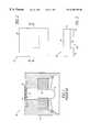
- FIG. 1is a cross-sectional view of a typical electrochemical gas sensor of the relevant art
- FIG. 2is a top plan view of a substrate assembly of an electrochemical gas sensor according to the present invention after formation of an etching mask;
- FIG. 3is a cross-sectional side-view of the substrate assembly of FIG. 2;
- FIG. 4is a top plan view of the substrate assembly of FIG. 2 after formation of a contact pad
- FIG. 5is a cross-sectional side-view of the substrate assembly of FIG. 4;
- FIG. 8is a top plan view of the substrate assembly of FIG. 6 after formation of a sensing electrode
- FIG. 10is top plan view of the substrate assembly of FIG. 8 after formation of a diffusion barrier
- FIG. 11is a cross-sectional side-view of the substrate assembly of FIG. 10;
- FIG. 12is a top plan of the substrate assembly of FIG. 10 after etching of the substrate;
- FIG. 13is a cross-sectional side-view of the substrate assembly of FIG. 12;
- FIG. 14is a top plan view of the substrate assembly of FIG. 12 after patterning of the diffusion barrier;
- FIG. 15is a cross-sectional side-view of the substrate assembly of FIG. 16;
- FIG. 16is a cross-sectional side-view of the electrochemical gas sensor according to the present invention.
- FIG. 17is a cross-sectional view of an electrochemical gas sensor according to another embodiment of the present invention.
- FIG. 18is a top plan view of a substrate assembly at a stage in the process of manufacturing an electrochemical gas sensor according to another embodiment of the present invention.
- FIG. 19is a top plan view of an electrochemical gas sensor array according to the present invention.
- FIG. 20is a top plan view of an electrochemical gas sensor array according to another embodiment of the present invention.
- FIGS. 2-16illustrate various stages in the progression of forming an electrochemical gas sensor on a substrate assembly 40 according to the present invention.
- the substrate assembly 40includes a substrate 42 and a portion of the components of the electrochemical gas sensor.
- the substrate 42is the lowest layer of material on a wafer, such as for example, a single crystal silicon wafer.
- a portion of the components of the electrochemical gas sensormay be formed on the substrate 42 using, for example, microfabrication processes.
- Microfabricationalso known as micromachining, commonly refers to the use of known semiconductor processing techniques to fabricate devices known as micro-electromechanical systems (MEMS) devices.
- MEMS fabrication processesinvolve the sequential addition and removal of layers of material from a substrate layer through use of film deposition and etching techniques until the desired structure has been realized. Accordingly, MEMS devices typically function under the same principles as their macroscale counterparts. MEMS devices, however, offer advantages in design, performance, and cost in comparison to their macroscale counterparts due to the decrease in scale of MEMS devices. In addition, due to batch fabrication techniques applicable to MEMS technology, significant reductions in per unit cost may be realized.
- MEMS fabrication techniqueshave been largely derived from the semiconductor industry. Accordingly, such techniques allow for the formation of structures on a substrate using adaptations of patterning, deposition, etching, and other processes that were originally developed for semiconductor fabrication. In general, these processes start with a substrate, such as a wafer of silicon. Multiple devices are then fabricated from the wafer through sequential addition and removal of layers of material. For example, various film deposition technologies, such as vacuum deposition, spin coating, dip coating, and screen printing may be used for thin film and thick film deposition of layers on the substrate. Layers of thin film may be removed, for example, by wet or dry surface etching, and parts of the substrate may be removed by, for example, wet or dry bulk etching.
- a substratesuch as a wafer of silicon.
- Multiple devicesare then fabricated from the wafer through sequential addition and removal of layers of material.
- various film deposition technologiessuch as vacuum deposition, spin coating, dip coating, and screen printing may be used for thin film and thick film deposition of layers on the substrate
- the waferis sectioned, or diced, to form multiple individual MEMS devices.
- the individual devicesare then packaged to provide for electrical connection of the devices into larger systems and components.
- the processes used for external packaging of the MEMS devicesare generally analogous to those used in semiconductor manufacturing.
- MEMS deviceshave the desirable feature that multiple MEMS devices may be produced simultaneously in a single batch by processing many individual components on a single wafer. For example, numerous individual electrochemical gas sensors may be formed on a single silicon substrate. Accordingly, the ability to produce numerous electrochemical gas sensors in a single batch results in a cost saving in comparison to the serial nature in which relevant art electrochemical gas sensors are manufactured.
- an electrochemical gas sensor manufactured according to MEMS fabrication techniquesallows for smaller electrochemical gas sensors, which in turn provides faster response times because of the decreased thickness of the diffusion layer.
- An electrochemical gas sensor according to the present inventionmay be used, for example, in medical applications, such as in a ventilator to monitor the in situ oxygen level of a patient.
- FIGS. 2 and 3illustrate a top plan view and a cross-sectional side view, respectively, of an electrochemical gas sensor having the substrate assembly 40 according to the present invention at an early stage in the fabrication thereof.
- the substrate assembly 40includes the substrate 42 and a portion of the components of the electrochemical gas sensor. As described hereinbelow, the portion of the components of the gas sensor are formed directly on the substrate 42 as various additional layers or structures, although, in other embodiments, the components may be formed on one or more intervening layers.
- the substrate assembly 40 illustrated in FIGS. 2 and 3further includes an etching mask 44 .
- the substrate 42is a non-conducting material such as, for example, a single crystal silicon wafer.
- the substrate 42has a first surface 46 and a second surface 48 .
- the etching mask 44is formed on the second surface 48 of the substrate 42 , and may be any material resistant to bulk etching of the substrate 42 such as, for example, silicon nitride.
- the etching mask 44may be formed on the substrate 42 by, for example, chemical vapor deposition. After the etching mask 44 is formed, it is patterned, such as by a conventional surface etch, to form a bulk etching area 50 .
- FIGS. 4 and 5illustrate the substrate assembly 40 with a contact pad 52 formed on the first surface 46 of the substrate 42 .
- the contact pad 52provides a surface for external connection of the sensor after final assembly, as described hereinbelow.
- the contact pad 52is an electrically conductive material such as, for example, gold or aluminum, and may be formed by conventional thin film deposition techniques, such as vacuum deposition or screen printing.
- the contact pad 52may be patterned to the desired shape and orientation using, for example, conventional surface etching techniques.
- FIGS. 6 and 7illustrate the substrate assembly 40 with a sensing electrode lead 54 formed on the first surface 46 of the substrate 42 .
- the sensing electrode lead 54is an electrically conductive material such as, for example, a noble metal such as silver, gold, platinum, or rhodium, and may be formed using conventional film deposition and surface etching techniques.
- the sensing electrode lead 54is in electrical contact with the contact pad 52 , and may also define an opening 56 for a sensing electrode 58 , as described hereinbelow with reference to FIGS. 8 and 9.
- FIGS. 8 and 9illustrate the substrate assembly 40 with the sensing electrode 58 formed on the first surface 46 of the substrate 42 .
- the sensing electrode 58is an electrically conductive material such as, for example, a noble metal, such as gold, silver, platinum, or rhodium.
- the sensing electrode 58is in electrical contact with the sensing electrode lead 54 , such as according to the embodiment illustrated in FIGS. 8 and 9, in which the sensing electrode 58 is formed within the opening 56 defined by the sensing electrode lead 54 .
- the sensing electrode 58may be formed according to conventional film deposition and patterning techniques.
- FIGS. 10 and 11illustrate the substrate assembly 40 with a diffusion barrier 60 formed on the first surface 46 of the substrate 42 before patterning of the diffusion barrier 60 .
- the diffusion barrier 60may be a hydrophobic material such as, for example, Teflon® fluoropolymer resin.
- the diffusion barrier 60before patterning, is in contact with the contact pad 52 , the sensing electrode lead 54 , the sensing electrode 58 , and the substrate 42 .
- the diffusion barrier 60may be deposited by conventional thin film deposition techniques, allowing the thickness of the diffusion barrier to be as small as one micron.
- FIGS. 12 and 13illustrate the substrate assembly 40 after a portion of the substrate 42 has been removed defining a cavity 62 .
- the cavity 62may be formed, for example, by anisotropic bulk etching of the substrate 42 . Only that portion of the substrate 42 exposed by the etching mask 44 is removed. The cavity 62 extends from the second surface 48 to the first surface 46 , exposing the sensing electrode 58 . Performing the bulk etching of the substrate 42 prior to patterning the diffusion barrier 60 permits the diffusion barrier 60 to act as a mask for the first surface 46 of the substrate 42 .
- FIGS. 14 and 15illustrate the substrate assembly 40 after patterning of the diffusion barrier 60 .
- the diffusion barrier 60is patterned, such as by conventional surface etching techniques, to expose the contact pad 52 . However, the diffusion barrier 60 remains in contact with the sensing electrode 58 , the sensing electrode lead 54 , and the substrate 42 after patterning. Because MEMS fabrication techniques allow the thickness of the diffusion barrier 60 to be on the order of one micron, as described hereinbefore, the response time of the sensor with the substrate assembly 40 having the sensing electrode 58 and the diffusion barrier 60 formed thereon may be less than one hundred ms. Moreover, using MEMS fabrication techniques allows the final assembly of the sensor to be much smaller than conventional electrochemical gas sensors, having a volume of approximately 10 cubic millimeters.
- FIG. 16illustrates a cross-sectional side-view of an electrochemical gas sensor 63 according to the present invention having the substrate assembly 40 .
- the gas sensor 63includes a housing 64 , a counter electrode 66 , and an electrolyte 68 added to the substrate assembly 40 .
- the housing 64protects the substrate assembly 40 and may be constructed of an electrically insulating material such as, for example, plastic or ceramic.
- the etching mask 44may remain on the substrate assembly 40 , as illustrated in FIG. 16, or it may be removed.
- the counter electrode 66is an electrically conductive material such as, for example, lead. The counter electrode 66 may be connected to the housing 64 and the substrate assembly 40 .
- the counter electrode 66is formed on a second substrate assembly 70 using, for example, MEMS fabrication techniques, as described hereinbefore. According to this embodiment, the second substrate assembly 70 is then bonded to the substrate assembly 40 using, for example, conventional wafer bonding techniques.
- the electrolyte 68may be, for example, an aqueous solution of potassium hydroxide.
- the electrolyte 68fills the cavity 62 in the substrate 42 , thereby forming an electrochemical cell between the sensing electrode 58 and the counter electrode 66 .
- FIG. 18is a top plan view of the substrate assembly 40 having an integrated resistance temperature detector (RTD) as a second sensing element formed on the substrate assembly 40 .
- RTDresistance temperature detector
- a thin film 72 of metal, such as platinum,is deposited on the first surface 46 of the substrate 42 adjacent the sensing electrode lead 54 .
- the thin film 72may be, for example, laser trimmed to a desired aspect ratio to form the RTD.
- a second contact pad 74 in electrical contact with the thin film 72may be formed on the substrate 42 in the same or similar fashion that the contact pad 52 was formed.
- the second contact pad 74permits the resistant measurement for the monitoring of temperature in the environment of the sensing electrode 58 . According to this embodiment, it is possible to do an in-situ temperature compensation of the sensor output, which may be desirous in certain applications, such as oxygen monitoring in an air-way of a ventilator.
- the RTD structure illustrated in FIG. 18is but one example of a component which may be integrated with the sensor 63 according to the present invention.
- Any electrical circuit capable of being formed on the substrate assembly 40such as, for example, compensating electrical circuits, may be integrated with the sensor 63 .
- other gas sensorsmay be integrated on the substrate.
- sensors which detect separate gasesmay be formed on a single substrate 42 to form a gas sensor array 80 , as illustrated in FIG. 19, which illustrates the array 80 at one stage in the process of manufacturing the array 80 .
- the embodiment illustrated in FIG. 19depicts the substrate assemblies 40 for an array 80 of nine sensors, although in other embodiments a different number of sensors may be formed on the substrate 42 .
- the various sensors comprising the array 80may detect different gases.
- different electrolytessuch as, for example, sulfuric acid and phosphoric acid, may be used.
- Different materials for forming the sensing electrodes 58 and the diffusion barriers 60need not be used, however, to create sensors which detect different gases, thus simplifying the process of manufacturing the array 80 .
- an array 80 of sensors built on the MEMS levelare much smaller than conventional relevant art gas sensor arrays because of the reduced scale of MEMS devices in comparison to their macroscale counterparts.
- FIG. 20illustrates another embodiment of an electrochemical gas sensor array 80 according to the present invention.
- one diffusion barrier 60is in contact with the sensing electrodes 58 .
- the diffusion barrier 60is patterned to expose the contact pads 52 .
Landscapes
- Chemical & Material Sciences (AREA)
- Life Sciences & Earth Sciences (AREA)
- Health & Medical Sciences (AREA)
- Physics & Mathematics (AREA)
- Chemical Kinetics & Catalysis (AREA)
- Electrochemistry (AREA)
- Molecular Biology (AREA)
- Analytical Chemistry (AREA)
- Biochemistry (AREA)
- General Health & Medical Sciences (AREA)
- General Physics & Mathematics (AREA)
- Immunology (AREA)
- Pathology (AREA)
- Measuring Oxygen Concentration In Cells (AREA)
Abstract
Description
Claims (31)
Priority Applications (1)
| Application Number | Priority Date | Filing Date | Title |
|---|---|---|---|
| US09/353,907US6265750B1 (en) | 1999-07-15 | 1999-07-15 | Electrochemical gas sensor and method of making the same |
Applications Claiming Priority (1)
| Application Number | Priority Date | Filing Date | Title |
|---|---|---|---|
| US09/353,907US6265750B1 (en) | 1999-07-15 | 1999-07-15 | Electrochemical gas sensor and method of making the same |
Publications (1)
| Publication Number | Publication Date |
|---|---|
| US6265750B1true US6265750B1 (en) | 2001-07-24 |
Family
ID=23391096
Family Applications (1)
| Application Number | Title | Priority Date | Filing Date |
|---|---|---|---|
| US09/353,907Expired - LifetimeUS6265750B1 (en) | 1999-07-15 | 1999-07-15 | Electrochemical gas sensor and method of making the same |
Country Status (1)
| Country | Link |
|---|---|
| US (1) | US6265750B1 (en) |
Cited By (12)
| Publication number | Priority date | Publication date | Assignee | Title |
|---|---|---|---|---|
| US20050014306A1 (en)* | 2003-07-15 | 2005-01-20 | Agency For Science, Technology And Research | Micromachined electromechanical device |
| US20050022811A1 (en)* | 2003-08-01 | 2005-02-03 | Herbert Kiesele | Measuring system for the determination of the concentration of propofol (2,6-diisopropylphenol) in the respiratory flow |
| US20060196245A1 (en)* | 2005-03-03 | 2006-09-07 | Tsinghua University | Reference leak and process for making same |
| US20090301876A1 (en)* | 2006-11-01 | 2009-12-10 | Mark Wagner | Sensor and methods of making the same |
| US7664607B2 (en) | 2005-10-04 | 2010-02-16 | Teledyne Technologies Incorporated | Pre-calibrated gas sensor |
| US20100294661A1 (en)* | 2009-05-22 | 2010-11-25 | Medical Graphics Corporation | Oxygen Sensor Improvement Method |
| US20170102355A1 (en)* | 2015-10-09 | 2017-04-13 | Patrick M. McGuinness | Electrochemical sensor, and a method of forming an electrochemical sensor |
| US10620151B2 (en) | 2016-08-30 | 2020-04-14 | Analog Devices Global | Electrochemical sensor, and a method of forming an electrochemical sensor |
| US11022579B2 (en) | 2018-02-05 | 2021-06-01 | Analog Devices International Unlimited Company | Retaining cap |
| US11268927B2 (en) | 2016-08-30 | 2022-03-08 | Analog Devices International Unlimited Company | Electrochemical sensor, and a method of forming an electrochemical sensor |
| US20230163034A1 (en)* | 2021-11-22 | 2023-05-25 | Industrial Technology Research Institute | Gas-permeable package lid of chip package structure and manufacturing method thereof |
| US12188893B2 (en) | 2016-08-30 | 2025-01-07 | Analog Devices International Unlimited Company | Electrochemical sensor, and a method of forming an electrochemical sensor |
Citations (9)
| Publication number | Priority date | Publication date | Assignee | Title |
|---|---|---|---|---|
| US4668374A (en)* | 1986-07-07 | 1987-05-26 | General Motors Corporation | Gas sensor and method of fabricating same |
| US4874500A (en)* | 1987-07-15 | 1989-10-17 | Sri International | Microelectrochemical sensor and sensor array |
| US5102525A (en)* | 1989-12-14 | 1992-04-07 | Hitachi, Ltd. | Planar oxygen sensor |
| US5183549A (en)* | 1990-01-26 | 1993-02-02 | Commtech International Management Corporation | Multi-analyte sensing electrolytic cell |
| GB2267348A (en)* | 1992-05-26 | 1993-12-01 | Walter John King | Electrochemical oxygen sensor |
| US5310610A (en)* | 1988-05-07 | 1994-05-10 | Sharp Kabushiki Kaisha | Silicon micro sensor and manufacturing method therefor |
| US5788832A (en) | 1996-07-19 | 1998-08-04 | Teledyne Industries, Inc. | Temperature compensated electrochemical gas sensor and method for closely tracking the temperature variations of a gas to be sensed |
| US5837454A (en) | 1988-11-14 | 1998-11-17 | I-Stat Corporation | Process for the manufacture of wholly microfabricated biosensors |
| US5883009A (en) | 1996-07-31 | 1999-03-16 | Sgs-Thomson Microelectronics S.R.L. | Method of fabricating integrated semiconductor devices comprising a chemoresistive gas microsensor |
- 1999
- 1999-07-15USUS09/353,907patent/US6265750B1/ennot_activeExpired - Lifetime
Patent Citations (9)
| Publication number | Priority date | Publication date | Assignee | Title |
|---|---|---|---|---|
| US4668374A (en)* | 1986-07-07 | 1987-05-26 | General Motors Corporation | Gas sensor and method of fabricating same |
| US4874500A (en)* | 1987-07-15 | 1989-10-17 | Sri International | Microelectrochemical sensor and sensor array |
| US5310610A (en)* | 1988-05-07 | 1994-05-10 | Sharp Kabushiki Kaisha | Silicon micro sensor and manufacturing method therefor |
| US5837454A (en) | 1988-11-14 | 1998-11-17 | I-Stat Corporation | Process for the manufacture of wholly microfabricated biosensors |
| US5102525A (en)* | 1989-12-14 | 1992-04-07 | Hitachi, Ltd. | Planar oxygen sensor |
| US5183549A (en)* | 1990-01-26 | 1993-02-02 | Commtech International Management Corporation | Multi-analyte sensing electrolytic cell |
| GB2267348A (en)* | 1992-05-26 | 1993-12-01 | Walter John King | Electrochemical oxygen sensor |
| US5788832A (en) | 1996-07-19 | 1998-08-04 | Teledyne Industries, Inc. | Temperature compensated electrochemical gas sensor and method for closely tracking the temperature variations of a gas to be sensed |
| US5883009A (en) | 1996-07-31 | 1999-03-16 | Sgs-Thomson Microelectronics S.R.L. | Method of fabricating integrated semiconductor devices comprising a chemoresistive gas microsensor |
Cited By (22)
| Publication number | Priority date | Publication date | Assignee | Title |
|---|---|---|---|---|
| CN100448046C (en)* | 2003-07-15 | 2008-12-31 | 新加坡科技研究局 | Method for manufacturing a piezoelectric film of a micromachined device |
| US7018862B2 (en)* | 2003-07-15 | 2006-03-28 | Agency For Science, Technology And Research | Micromachined electromechanical device |
| US20060068564A1 (en)* | 2003-07-15 | 2006-03-30 | Agency For Science, Technology And Research | Micromachined electromechanical device |
| US20050014306A1 (en)* | 2003-07-15 | 2005-01-20 | Agency For Science, Technology And Research | Micromachined electromechanical device |
| US7208806B2 (en) | 2003-07-15 | 2007-04-24 | Agency For Science, Technology And Research | Micromachined electromechanical device |
| US20050022811A1 (en)* | 2003-08-01 | 2005-02-03 | Herbert Kiesele | Measuring system for the determination of the concentration of propofol (2,6-diisopropylphenol) in the respiratory flow |
| US7364552B2 (en)* | 2003-08-01 | 2008-04-29 | DRäGERWERK AKTIENGESELLSCHAFT | Measuring system for the determination of the concentration of propofol (2,6-diisopropylphenol) in the respiratory flow |
| US7814773B2 (en)* | 2005-03-03 | 2010-10-19 | Tsinghua University | Reference leak |
| US20060196245A1 (en)* | 2005-03-03 | 2006-09-07 | Tsinghua University | Reference leak and process for making same |
| US7664607B2 (en) | 2005-10-04 | 2010-02-16 | Teledyne Technologies Incorporated | Pre-calibrated gas sensor |
| US20090301876A1 (en)* | 2006-11-01 | 2009-12-10 | Mark Wagner | Sensor and methods of making the same |
| US8266795B2 (en) | 2006-11-01 | 2012-09-18 | Sensorcon, Inc. | Methods of making an electrochemical gas sensor |
| US20100294661A1 (en)* | 2009-05-22 | 2010-11-25 | Medical Graphics Corporation | Oxygen Sensor Improvement Method |
| US8110081B2 (en) | 2009-05-22 | 2012-02-07 | Medical Graphics Corporation | Oxygen sensor improvement method |
| US20170102355A1 (en)* | 2015-10-09 | 2017-04-13 | Patrick M. McGuinness | Electrochemical sensor, and a method of forming an electrochemical sensor |
| US10620151B2 (en) | 2016-08-30 | 2020-04-14 | Analog Devices Global | Electrochemical sensor, and a method of forming an electrochemical sensor |
| US11268927B2 (en) | 2016-08-30 | 2022-03-08 | Analog Devices International Unlimited Company | Electrochemical sensor, and a method of forming an electrochemical sensor |
| US12188893B2 (en) | 2016-08-30 | 2025-01-07 | Analog Devices International Unlimited Company | Electrochemical sensor, and a method of forming an electrochemical sensor |
| US11022579B2 (en) | 2018-02-05 | 2021-06-01 | Analog Devices International Unlimited Company | Retaining cap |
| US11959876B2 (en) | 2018-02-05 | 2024-04-16 | Analog Devices International Unlimited Company | Retaining cap |
| US20230163034A1 (en)* | 2021-11-22 | 2023-05-25 | Industrial Technology Research Institute | Gas-permeable package lid of chip package structure and manufacturing method thereof |
| US12191219B2 (en)* | 2021-11-22 | 2025-01-07 | Industrial Technology Research Institute | Gas-permeable package lid of chip package structure and manufacturing method thereof |
Similar Documents
| Publication | Publication Date | Title |
|---|---|---|
| EP0744603B1 (en) | Linear capacitive sensor by fixing the center of a membrane | |
| US6445053B1 (en) | Micro-machined absolute pressure sensor | |
| EP1436582B1 (en) | Pressure sensor | |
| EP0720731B1 (en) | Suspended diaphragm pressure sensor | |
| US8961760B2 (en) | Micromechanical solid-electrolyte sensor device and corresponding production method | |
| US20070275495A1 (en) | Method for fabricating a pressure sensor using SOI wafers | |
| US7998777B1 (en) | Method for fabricating a sensor | |
| US6265750B1 (en) | Electrochemical gas sensor and method of making the same | |
| KR20090064693A (en) | Micro gas sensor and its manufacturing method | |
| AU2001280660A1 (en) | Micro-machined absolute pressure sensor | |
| US7051595B2 (en) | Monolithic multi-functional integrated sensor and method for fabricating the same | |
| EP1434048A1 (en) | CAPACITIVE HUMIDITY−SENSOR AND CAPACITIVE HUMIDITY−SENSOR MANUFACTURING METHOD | |
| TW201302598A (en) | Device for measuring environmental forces and method of fabricating the same | |
| US20160209344A1 (en) | Complex sensor and method of manufacturing the same | |
| CN113428829B (en) | MEMS (micro-electromechanical system) wet-pressing integrated sensor and preparation method thereof | |
| EP2759832B1 (en) | Electrochemical sensor device | |
| US4872945A (en) | Post seal etching of transducer diaphragm | |
| CN107250783A (en) | The method for being used for detecting the gas sensor device for measuring at least one of medium gaseous analytes for manufacturing and method and gas sensor device for detecting at least one of measurement medium gaseous analytes | |
| WO2017060769A1 (en) | An electrochemical sensor, and a method of forming an electrochemical sensor | |
| EP2873958A1 (en) | Capacitive pressure sensors for high temperature applications | |
| EP2492240A1 (en) | IC with pressure sensor and manufacturing method thereof | |
| CN116621112A (en) | MEMS four-in-one monolithic integrated sensor | |
| CN119604467A (en) | Packaging structure and preparation method thereof and sensor | |
| KR20050075225A (en) | Mems monolithic multi-functional integrated sensor and methods for fabricating the same | |
| US20240219252A1 (en) | Electronic components, detection method of pressure value and manufacturing method of electronic components |
Legal Events
| Date | Code | Title | Description |
|---|---|---|---|
| AS | Assignment | Owner name:TELEDYNE INDUSTRIES, INC., CALIFORNIA Free format text:ASSIGNMENT OF ASSIGNORS INTEREST;ASSIGNORS:FENG, CHANG-DONG;CHU, EDMOND Y.;REEL/FRAME:010108/0983 Effective date:19990630 | |
| STCF | Information on status: patent grant | Free format text:PATENTED CASE | |
| AS | Assignment | Owner name:TELEDYNE TECHNOLOGIES INCORPORATED, CALIFORNIA Free format text:ASSIGNMENT OF ASSIGNORS INTEREST;ASSIGNOR:TELEDYNE INDUSTRIES, INC.;REEL/FRAME:013146/0358 Effective date:19991129 | |
| FEPP | Fee payment procedure | Free format text:PAYOR NUMBER ASSIGNED (ORIGINAL EVENT CODE: ASPN); ENTITY STATUS OF PATENT OWNER: LARGE ENTITY | |
| FPAY | Fee payment | Year of fee payment:4 | |
| FPAY | Fee payment | Year of fee payment:8 | |
| AS | Assignment | Owner name:TELEDYNE INSTRUMENTS, INC., CALIFORNIA Free format text:ASSIGNMENT OF ASSIGNORS INTEREST;ASSIGNOR:TELEDYNE TECHNOLOGIES INCORPORATED;REEL/FRAME:027793/0127 Effective date:20111222 | |
| FPAY | Fee payment | Year of fee payment:12 |