US6265305B1 - Method of preventing corrosion of a titanium layer in a semiconductor wafer - Google Patents
Method of preventing corrosion of a titanium layer in a semiconductor waferDownload PDFInfo
- Publication number
- US6265305B1 US6265305B1US09/410,094US41009499AUS6265305B1US 6265305 B1US6265305 B1US 6265305B1US 41009499 AUS41009499 AUS 41009499AUS 6265305 B1US6265305 B1US 6265305B1
- Authority
- US
- United States
- Prior art keywords
- layer
- titanium
- semiconductor wafer
- photoresist
- cleaning process
- Prior art date
- Legal status (The legal status is an assumption and is not a legal conclusion. Google has not performed a legal analysis and makes no representation as to the accuracy of the status listed.)
- Expired - Lifetime
Links
Images


Classifications
- H—ELECTRICITY
- H01—ELECTRIC ELEMENTS
- H01L—SEMICONDUCTOR DEVICES NOT COVERED BY CLASS H10
- H01L21/00—Processes or apparatus adapted for the manufacture or treatment of semiconductor or solid state devices or of parts thereof
- H01L21/70—Manufacture or treatment of devices consisting of a plurality of solid state components formed in or on a common substrate or of parts thereof; Manufacture of integrated circuit devices or of parts thereof
- H01L21/71—Manufacture of specific parts of devices defined in group H01L21/70
- H01L21/768—Applying interconnections to be used for carrying current between separate components within a device comprising conductors and dielectrics
- H01L21/76838—Applying interconnections to be used for carrying current between separate components within a device comprising conductors and dielectrics characterised by the formation and the after-treatment of the conductors
- H01L21/76841—Barrier, adhesion or liner layers
- H01L21/76843—Barrier, adhesion or liner layers formed in openings in a dielectric
- H—ELECTRICITY
- H01—ELECTRIC ELEMENTS
- H01L—SEMICONDUCTOR DEVICES NOT COVERED BY CLASS H10
- H01L21/00—Processes or apparatus adapted for the manufacture or treatment of semiconductor or solid state devices or of parts thereof
- H01L21/70—Manufacture or treatment of devices consisting of a plurality of solid state components formed in or on a common substrate or of parts thereof; Manufacture of integrated circuit devices or of parts thereof
- H01L21/71—Manufacture of specific parts of devices defined in group H01L21/70
- H01L21/768—Applying interconnections to be used for carrying current between separate components within a device comprising conductors and dielectrics
- H01L21/76838—Applying interconnections to be used for carrying current between separate components within a device comprising conductors and dielectrics characterised by the formation and the after-treatment of the conductors
- H01L21/76841—Barrier, adhesion or liner layers
- H—ELECTRICITY
- H01—ELECTRIC ELEMENTS
- H01L—SEMICONDUCTOR DEVICES NOT COVERED BY CLASS H10
- H01L21/00—Processes or apparatus adapted for the manufacture or treatment of semiconductor or solid state devices or of parts thereof
- H01L21/02—Manufacture or treatment of semiconductor devices or of parts thereof
- H01L21/04—Manufacture or treatment of semiconductor devices or of parts thereof the devices having potential barriers, e.g. a PN junction, depletion layer or carrier concentration layer
- H01L21/18—Manufacture or treatment of semiconductor devices or of parts thereof the devices having potential barriers, e.g. a PN junction, depletion layer or carrier concentration layer the devices having semiconductor bodies comprising elements of Group IV of the Periodic Table or AIIIBV compounds with or without impurities, e.g. doping materials
- H01L21/30—Treatment of semiconductor bodies using processes or apparatus not provided for in groups H01L21/20 - H01L21/26
- H01L21/31—Treatment of semiconductor bodies using processes or apparatus not provided for in groups H01L21/20 - H01L21/26 to form insulating layers thereon, e.g. for masking or by using photolithographic techniques; After treatment of these layers; Selection of materials for these layers
- H01L21/3105—After-treatment
- H01L21/311—Etching the insulating layers by chemical or physical means
- H01L21/31127—Etching organic layers
- H01L21/31133—Etching organic layers by chemical means
- H01L21/31138—Etching organic layers by chemical means by dry-etching
- Y—GENERAL TAGGING OF NEW TECHNOLOGICAL DEVELOPMENTS; GENERAL TAGGING OF CROSS-SECTIONAL TECHNOLOGIES SPANNING OVER SEVERAL SECTIONS OF THE IPC; TECHNICAL SUBJECTS COVERED BY FORMER USPC CROSS-REFERENCE ART COLLECTIONS [XRACs] AND DIGESTS
- Y10—TECHNICAL SUBJECTS COVERED BY FORMER USPC
- Y10S—TECHNICAL SUBJECTS COVERED BY FORMER USPC CROSS-REFERENCE ART COLLECTIONS [XRACs] AND DIGESTS
- Y10S438/00—Semiconductor device manufacturing: process
- Y10S438/976—Temporary protective layer
Definitions
- the present inventionrelates to a method of preventing corrosion of a titanium layer in a semiconductor wafer.
- a dielectric layeris normally positioned between the MOS (Metal Oxide Semiconductor) transistor and each of the metal conducting wire in a semiconductor wafer for separating and protecting the components in the semiconductor wafer.
- MOSMetal Oxide Semiconductor
- a contact plug formed in the dielectric layeris necessary to be used as a conducting wire between the MOS and each corresponding metal conducting wire. Therefore, just how to upgrade the quality of process for manufacturing the contact plug and the metal wire layer has become an important subject matter in the study of the process for manufacturing the semiconductor.
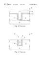
- FIG. 1 and FIG. 2are the prior art's schematic diagrams of the manufacturing process of the contact plug 24 of the semiconductor wafer 10 .
- the semiconductor wafer 10comprises a bottom conducting layer 12 and a dielectric layer 14 positioned at the top of the bottom conducting layer 12 .
- conventional process for manufacturing the contact plug 24is first to perform photolithography and etching processes in order to form a contact hole 16 , then to deposit in sequence, on the surfaces of the semiconductor wafer 10 and the contact hole 16 , a titanium layer 18 , a TiN (titanium nitride) layer 20 , and a conducting layer 22 composed of tungsten. Thereafter, as shown in FIG.
- FIG. 3 and FIG. 4are the prior art's schematic diagrams of the manufacturing process of the metal wire 40 of the semiconductor wafer 10 .
- a normal metallization processcontinues to manufacture the metal wire 40 such that the bottom conducting layer 12 connects to the other components in the semiconductor wafer 10 through the contact plug 24 and the metal wire 40 to gradually form a complete circuit.
- the conventional way of fabricating the metal wire 40is first to uniformly deposit, on the surface of the dielectric layer 14 and the top of the contact plug 24 , a titanium layer 26 and a protecting layer 28 composed of TiN, it then to form in sequence, on the protecting layer 28 , an aluminum conducting layer 30 and an anti-reflective coating layer 32 composed of TiN, in the mean time, to define and form the pattern of metal wire 40 by the use of the photolithography and etching processes.
- misalignment of the metal wire 40often occurs due to the limitation of the manufacturing techniques or other factors, that is to say, the patterned photoresist layer 34 used for defining the metal wire 40 is unable to completely cover right at the top of the contact plug 24 even though there is a certain tolerance range in this metal misalignment phenomenon, in other words, only a portion of the metal wire 40 covers on top of the contact plug 24 .
- the primary objective of the present inventionis to provide a method of preventing corrosion of a titanium layer in a semiconductor wafer to effectively resolve the problem that the joint interface between the metal wire and the contact plug positioned underneath is exposed to the photoresist stripper solution such that the titanium layer is subject to be corroded due to the electrochemical reaction.
- FIG. 1 and FIG. 2are the prior art's schematic diagrams of the manufacturing process of the contact plug of the semiconductor wafer.
- FIG. 3 and FIG. 4are the prior art's schematic diagrams of the manufacturing process of the metal wire of the semiconductor wafer.
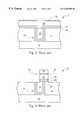
- FIG. 5 to FIG. 8are the schematic diagrams of the manufacturing process of the metal wire of the semiconductor wafer of the present invention.
- FIG. 5 to FIG. 8are the schematic diagrams of the manufacturing process of the metal wire 76 of the semiconductor wafer 50 of the present invention.
- the present inventionprovides a method of preventing corrosion of a titanium layer in a semiconductor wafer. The method can be applied in the manufacturing process of the metal wire at the top of the contact plug.
- the semiconductor wafer 50comprises a bottom conducting layer 52 and a dielectric layer 54 positioned at the top of the bottom conduction layer 52 .
- the dielectric layer 54comprises a through hole used as a contact hole 56 (or as a via hole).
- the method of the present inventionis first to uniformly deposit in sequence, on the surface of the semiconductor wafer 50 and the contact hole 56 , a glue layer 58 composed of titanium, a barrier layer 60 composed of TiN, and a conducting layer 62 composed of tungsten.
- the barrier layer 60can prevent titanium in the glue layer 58 from being corroded and can bar the metal ion from invading through the semiconductor components positioned underneath, thus affecting the normal operation of the semiconductor components.
- a surface treatmentis performed on the semiconductor wafer 50 by CMP method to uniformly remove the conducting layer 62 , the barrier layer 60 , and the glue layer 58 on the surface of the dielectric layer 54 in order to form a tungsten plug 64 and to cut the top of the tungsten plug 64 at the same level as that of the surface of the dielectric layer 54 so as to the tungsten plug 64 is a kind of column-shaped structure embedded in the dielectric layer 54 and having an annular vertical side wall 65 .
- the fabrication process of the metal wirewill be continued to connect the bottom conducting layer 52 to the other components on the semiconductor wafer 50 through the tungsten plug 64 and metal wire in order to gradually form a complete circuit.
- the fabrication process of the metal wireis first to uniformly deposit, on the surface of dielectric layer 54 and at the top of tungsten plug 64 , a titanium layer 66 and a protection layer 68 composed of TiN, then to form in sequence, on the protecting layer 68 , an aluminum conducting layer 70 composed of copper-aluminum alloy and an anti-reflective coating layer 72 composed of TiN.
- the protecting layer 68 , the aluminum conducting layer 70 , and the anti-reflective coating layer 72together form a main conducting layer 76 of the metal wire.
- the protecting layer 68is used for preventing the copper-aluminum alloy in the aluminum conducting layer 70 and the titanium in the titanium layer 66 from chemical reaction.
- a layer of photoresist layer 74is uniformly coated on the surface of the semi-conductor wafer 50 , and then the photolithography and etching processes are used to define and form a predetermined pattern of metal wire 77 . While performing the etching process for forming the metal wire 77 , a lot of polymers will be generated that are scattering around and are deposited on the surface of the semiconductor wafer 50 to form a polymer layer (not shown in FIG. 8 ). Therefore, a dry cleaning process is then performed in a vacuum chamber of the etching process to roughly eliminate the polymer layer and the photoresist layer 74 on the surface of the semiconductor wafer 50 .
- the dry cleaning process of the present inventionis to introduce oxygen in the vacuum chamber to perform a plasma process, or to introduce carbon tetrafluoride (CF 4 ) in an environment containing oxygen to act as reacting gas, and to perform a dry cleaning process by the use of plasma.
- CF 4carbon tetrafluoride
- a nitridizing processis performed to introduce nitrogen (N 2 ), ammonia (NH 3 ) or other nitrogenous gases into the vacuum chamber to form a plasma environment containing nitrogen such that the surface of the titanium layer 66 exposed to the surface of the semiconductor wafer 50 is reacted to generate a TiN layer (not shown in FIG. 8 ).
- a wet cleaning processis performed by the use of a standard photoresist stripper solution to entirely strip off the polymer and the photoresist layer 74 remained on the surface of the semiconductor wafer 50 , thus the fabrication process of metal wire 77 is completed.
- the joint interface 78is in no way to be exposed to the surface of the semiconductor wafer 50 .
- the photoresist stripper solutionis by no means to contact the titanium-tungsten joint interface 78 , the electrochemical reaction between the titanium and tungsten is unable to occur in exposing in the environment of photoresist stripper solution.
- the method of the present inventioncan prevent the titanium layer 66 at the top of the tungsten plug 64 from being corroded.
- the method of the present inventionto form a TiN layer at the top of the titanium layer 66 can also prevent the titanium layer 66 from being corroded by the photoresist stripper solution.
- the method of the present inventioncan also prevent the titanium layer 66 at the top of the tungsten plug 64 from being corroded.
- the method of the present inventionto fabricate the tungsten plug 64 and the metal wire 77 at the top of the tungsten plug 64 can increase the tolerance range of misalignment for the metal wire 74 .
- the method of the present invention for fabricating the metal wire 77not only can be applied in connecting the plug in the contact hole but also can be applied in connecting the plug in other holes.
- the metal wire's manufacturing process according to the present inventionis first to utilize a plasma environment containing nitrogen to perform a nitridizing process in order to make the surface of the titanium layer exposed to the surface of the semiconductor wafer to generate a TiN layer. Thereafter, the wet cleaning process is performed to strip off the photoresist. Since there is a TiN layer on the titanium layer at the top of the tungsten plug, it is in no way that a electrochemical reaction occurs between the titanium and the tungsten under the environment of photoresist stripper solution. As the method of the present invention can prevent the titanium from being corroded, the integration of the contact interface between the metal wire and the plug can be kept. In addition, the range of the positioning tolerance of the metal wire can be relatively increased.
Landscapes
- Engineering & Computer Science (AREA)
- Physics & Mathematics (AREA)
- Condensed Matter Physics & Semiconductors (AREA)
- General Physics & Mathematics (AREA)
- Manufacturing & Machinery (AREA)
- Computer Hardware Design (AREA)
- Microelectronics & Electronic Packaging (AREA)
- Power Engineering (AREA)
- Internal Circuitry In Semiconductor Integrated Circuit Devices (AREA)
Abstract
Description
1. Field of the Invention
The present invention relates to a method of preventing corrosion of a titanium layer in a semiconductor wafer.
2. Description of the Prior Art
A dielectric layer is normally positioned between the MOS (Metal Oxide Semiconductor) transistor and each of the metal conducting wire in a semiconductor wafer for separating and protecting the components in the semiconductor wafer. In order to successfully connect these components in the MOS to each of the metal conducting wire so as to form a complete electronic device, a contact plug formed in the dielectric layer is necessary to be used as a conducting wire between the MOS and each corresponding metal conducting wire. Therefore, just how to upgrade the quality of process for manufacturing the contact plug and the metal wire layer has become an important subject matter in the study of the process for manufacturing the semiconductor.
Please refer to FIG.1 and FIG.2. FIG.1 and FIG. 2 are the prior art's schematic diagrams of the manufacturing process of thecontact plug 24 of thesemiconductor wafer 10. Thesemiconductor wafer 10 comprises a bottom conductinglayer 12 and adielectric layer 14 positioned at the top of thebottom conducting layer 12. As shown in FIG. 1, conventional process for manufacturing thecontact plug 24 is first to perform photolithography and etching processes in order to form acontact hole 16, then to deposit in sequence, on the surfaces of thesemiconductor wafer 10 and thecontact hole 16, atitanium layer 18, a TiN (titanium nitride)layer 20, and a conductinglayer 22 composed of tungsten. Thereafter, as shown in FIG. 2, by the use of CMP(Chemical Mechanical Polishing)process to perform a surface treatment on thesemiconductor wafer 10 to uniformly remove the conductinglayer 22, theTiN layer 20, and thetitanium layer 18 on the surface of thedielectric layer 14 in order to form acontact plug 24, and in the mean time, to cut the top of thecontact plug 24 to be at the same level as that of thedielectric layer 14.
Please refer to FIG.3 and FIG.4. FIG.3 and FIG. 4 are the prior art's schematic diagrams of the manufacturing process of the metal wire40 of thesemiconductor wafer 10. After completing the fabrication process of thecontact plug 24, a normal metallization process continues to manufacture the metal wire40 such that thebottom conducting layer 12 connects to the other components in the semiconductor wafer10 through thecontact plug 24 and the metal wire40 to gradually form a complete circuit. The conventional way of fabricating the metal wire40 is first to uniformly deposit, on the surface of thedielectric layer 14 and the top of thecontact plug 24, atitanium layer 26 and a protectinglayer 28 composed of TiN, it then to form in sequence, on the protectinglayer 28, an aluminum conductinglayer 30 and ananti-reflective coating layer 32 composed of TiN, in the mean time, to define and form the pattern of metal wire40 by the use of the photolithography and etching processes.
As shown in FIG. 4, while fabricating the metal wire40, misalignment of the metal wire40 often occurs due to the limitation of the manufacturing techniques or other factors, that is to say, the patternedphotoresist layer 34 used for defining the metal wire40 is unable to completely cover right at the top of thecontact plug 24 even though there is a certain tolerance range in this metal misalignment phenomenon, in other words, only a portion of the metal wire40 covers on top of thecontact plug 24.
Since only a portion of the metal wire40 covers on top of thecontact plug 24, a portion of the conductinglayer 22 andtitanium layer 26 will be exposed on the surface of thesemiconductor wafer 10. And since the tungsten's chemical potential is higher than that of the titanium, thetitanium layer 26 on the titanium-tungsten interface 38 is subject to be corroded by the photoresist stripper solution during the upcoming photoresist stripping process of thephotoresist layer 34. As a result, the corrosion situation will decrease the contact area between the metal wire40 and thecontact plug 24 and increase the resistance of thecontact plug 24 or increase the contact resistance between thecontact plug 24 and the metal wire40, or it will even cause a serious result of disconnection of the circuit.
Therefore, the primary objective of the present invention is to provide a method of preventing corrosion of a titanium layer in a semiconductor wafer to effectively resolve the problem that the joint interface between the metal wire and the contact plug positioned underneath is exposed to the photoresist stripper solution such that the titanium layer is subject to be corroded due to the electrochemical reaction.
FIG.1 and FIG. 2 are the prior art's schematic diagrams of the manufacturing process of the contact plug of the semiconductor wafer.
FIG.3 and FIG. 4 are the prior art's schematic diagrams of the manufacturing process of the metal wire of the semiconductor wafer.
FIG. 5 to FIG. 8 are the schematic diagrams of the manufacturing process of the metal wire of the semiconductor wafer of the present invention.
Please refer to FIGS. 5 to8. FIG. 5 to FIG. 8 are the schematic diagrams of the manufacturing process of themetal wire 76 of thesemiconductor wafer 50 of the present invention. The present invention provides a method of preventing corrosion of a titanium layer in a semiconductor wafer. The method can be applied in the manufacturing process of the metal wire at the top of the contact plug. As shown in FIG.5,thesemiconductor wafer 50 comprises a bottom conductinglayer 52 and adielectric layer 54 positioned at the top of thebottom conduction layer 52. Thedielectric layer 54 comprises a through hole used as a contact hole56 (or as a via hole).
In manufacturing the metal wire, the method of the present invention is first to uniformly deposit in sequence, on the surface of thesemiconductor wafer 50 and thecontact hole 56, aglue layer 58 composed of titanium, abarrier layer 60 composed of TiN, and a conductinglayer 62 composed of tungsten. In the upcoming manufacturing process, thebarrier layer 60 can prevent titanium in theglue layer 58 from being corroded and can bar the metal ion from invading through the semiconductor components positioned underneath, thus affecting the normal operation of the semiconductor components.
Thereafter, as shown in FIG. 6, a surface treatment is performed on thesemiconductor wafer 50 by CMP method to uniformly remove the conductinglayer 62, thebarrier layer 60, and theglue layer 58 on the surface of thedielectric layer 54 in order to form atungsten plug 64 and to cut the top of thetungsten plug 64 at the same level as that of the surface of thedielectric layer 54 so as to thetungsten plug 64 is a kind of column-shaped structure embedded in thedielectric layer 54 and having an annularvertical side wall 65.
As shown in FIG. 7, after the fabrication process of thetungsten plug 64 is completed, the fabrication process of the metal wire will be continued to connect thebottom conducting layer 52 to the other components on thesemiconductor wafer 50 through thetungsten plug 64 and metal wire in order to gradually form a complete circuit. The fabrication process of the metal wire is first to uniformly deposit, on the surface ofdielectric layer 54 and at the top oftungsten plug 64, atitanium layer 66 and aprotection layer 68 composed of TiN, then to form in sequence, on the protectinglayer 68, an aluminum conductinglayer 70 composed of copper-aluminum alloy and ananti-reflective coating layer 72 composed of TiN. The protectinglayer 68, the aluminum conductinglayer 70, and theanti-reflective coating layer 72 together form a main conductinglayer 76 of the metal wire. Among them, the protectinglayer 68 is used for preventing the copper-aluminum alloy in the aluminum conductinglayer 70 and the titanium in thetitanium layer 66 from chemical reaction. There is an alternative to cover the aluminum conductinglayer 70 directly on the surface of thetitanium layer 66.
As shown in FIG. 8, thereafter, a layer ofphotoresist layer 74 is uniformly coated on the surface of thesemi-conductor wafer 50, and then the photolithography and etching processes are used to define and form a predetermined pattern ofmetal wire 77. While performing the etching process for forming themetal wire 77, a lot of polymers will be generated that are scattering around and are deposited on the surface of thesemiconductor wafer 50 to form a polymer layer (not shown in FIG.8). Therefore, a dry cleaning process is then performed in a vacuum chamber of the etching process to roughly eliminate the polymer layer and thephotoresist layer 74 on the surface of thesemiconductor wafer 50. The dry cleaning process of the present invention is to introduce oxygen in the vacuum chamber to perform a plasma process, or to introduce carbon tetrafluoride (CF4) in an environment containing oxygen to act as reacting gas, and to perform a dry cleaning process by the use of plasma.
Afterward, a nitridizing process is performed to introduce nitrogen (N2), ammonia (NH3) or other nitrogenous gases into the vacuum chamber to form a plasma environment containing nitrogen such that the surface of thetitanium layer 66 exposed to the surface of thesemiconductor wafer 50 is reacted to generate a TiN layer (not shown in FIG.8). Finally, a wet cleaning process is performed by the use of a standard photoresist stripper solution to entirely strip off the polymer and thephotoresist layer 74 remained on the surface of thesemiconductor wafer 50, thus the fabrication process ofmetal wire 77 is completed.
By employing the method of the present invention in fabricating themetal wire 77, since the surface of thetitanium layer 66 exposed to the surface of thesemiconductor wafer 50 is reacted to generate first a protectinglayer 68 composed of TiN by using nitrogen or ammonia before the photoresist stripper process of performing the wet cleaning, thejoint interface 78 is in no way to be exposed to the surface of thesemiconductor wafer 50. While in performing the photoresist stripper process, since the photoresist stripper solution is by no means to contact the titanium-tungsten joint interface 78, the electrochemical reaction between the titanium and tungsten is unable to occur in exposing in the environment of photoresist stripper solution. Thereby, the method of the present invention can prevent thetitanium layer 66 at the top of thetungsten plug 64 from being corroded.
While employing the method of the present invention to fabricatetungsten plug 64 and themetal wire 77 on top of thetungsten plug 64, even though thephotoresist layer 74 is unable to entirely cover right at the top of thetungsten plug 64 which results in the fact that themetal wire 77 is unable to entirely overlap to cover right at the top of thetungsten plug 64, the method of the present invention to form a TiN layer at the top of thetitanium layer 66 can also prevent thetitanium layer 66 from being corroded by the photoresist stripper solution. In addition, the method of the present invention can also prevent thetitanium layer 66 at the top of thetungsten plug 64 from being corroded. Therefore, by employing the method of the present invention to fabricate thetungsten plug 64 and themetal wire 77 at the top of thetungsten plug 64 can increase the tolerance range of misalignment for themetal wire 74. Besides, the method of the present invention for fabricating themetal wire 77 not only can be applied in connecting the plug in the contact hole but also can be applied in connecting the plug in other holes.
In comparison to the method of metal wire's manufacturing process of the prior art, the metal wire's manufacturing process according to the present invention is first to utilize a plasma environment containing nitrogen to perform a nitridizing process in order to make the surface of the titanium layer exposed to the surface of the semiconductor wafer to generate a TiN layer. Thereafter, the wet cleaning process is performed to strip off the photoresist. Since there is a TiN layer on the titanium layer at the top of the tungsten plug, it is in no way that a electrochemical reaction occurs between the titanium and the tungsten under the environment of photoresist stripper solution. As the method of the present invention can prevent the titanium from being corroded, the integration of the contact interface between the metal wire and the plug can be kept. In addition, the range of the positioning tolerance of the metal wire can be relatively increased.
Those skilled in the art will readily observe that numerous modifications and alterations of the device may be made while retaining the teaching of the invention. Accordingly, the above disclosure should be construed as limited only by the metes and bounds of the appended claims.
Claims (8)
1. A method of preventing corrosion of a titanium layer in a semiconductor wafer, the semiconductor wafer comprising a dielectric layer, a column-shaped tungsten plug embedded in the dielectric layer and having its top surface cut to be at the same level as that of the surface of the dielectric layer, a patterned titanium layer positioned on the dielectric layer and covering a portion of the top surface of the tungsten plug comprising an exposed region, a main conductive layer positioned on the surface of the titanium layer, a photoresist layer positioned on the surface of the main conductive layer, and a polymer layer covered on the surface of the semiconductor wafer, the method comprising the following steps:
performing a dry cleaning process to partially remove the polymer layer and the photoresist layer;
performing a nitridizing process to form a titanium nitride layer on the exposed portion of the titanium layer; and
performing a wet cleaning process with a photoresist stripper solution to fully remove the residual photoresist layer and the polymer layer from the surface of the semiconductor wafer;
wherein the titanium nitride layer is used for preventing the titanium layer from being corroded by the photoresist stripper solution.
2. The method of claim1 wherein an O2 gas is inputted into a vacuum chamber to perform a plasma reaction in the dry cleaning process in which the polymer layer and the photoresist layer are partially removed.
3. The method of claim1 wherein the dry cleaning process comprises CF4as one of the reactants.
4. The method of the claim1 wherein the nitridizing process is performed in a vacuum chamber in which a nitrogen plasma is formed by inputting a nitrogen gas or an ammonia gas into the vacuum chamber.
5. The method of claim1 wherein the main conductive layer comprises an aluminum alloy layer.
6. The method of claim5 where the main conductive layer further comprises an anti-reflection layer positioned on the aluminum alloy layer and a protection layer positioned between the aluminum alloy layer and the titanium layer.
7. The method of claim6 wherein the anti-reflection layer is made of titanium nitride.
8. The method of claim1 wherein the column-shaped tungsten plug further comprises a titanium nitride layer working as a barrier layer on its outer side and a titanium layer working as a glue layer outside the barrier layer.
Priority Applications (1)
| Application Number | Priority Date | Filing Date | Title |
|---|---|---|---|
| US09/410,094US6265305B1 (en) | 1999-10-01 | 1999-10-01 | Method of preventing corrosion of a titanium layer in a semiconductor wafer |
Applications Claiming Priority (1)
| Application Number | Priority Date | Filing Date | Title |
|---|---|---|---|
| US09/410,094US6265305B1 (en) | 1999-10-01 | 1999-10-01 | Method of preventing corrosion of a titanium layer in a semiconductor wafer |
Publications (1)
| Publication Number | Publication Date |
|---|---|
| US6265305B1true US6265305B1 (en) | 2001-07-24 |
Family
ID=23623184
Family Applications (1)
| Application Number | Title | Priority Date | Filing Date |
|---|---|---|---|
| US09/410,094Expired - LifetimeUS6265305B1 (en) | 1999-10-01 | 1999-10-01 | Method of preventing corrosion of a titanium layer in a semiconductor wafer |
Country Status (1)
| Country | Link |
|---|---|
| US (1) | US6265305B1 (en) |
Cited By (9)
| Publication number | Priority date | Publication date | Assignee | Title |
|---|---|---|---|---|
| US6333261B1 (en) | 2000-06-01 | 2001-12-25 | United Microelectronics Corp. | Method for preventing aluminum intrusions |
| US20030020165A1 (en)* | 2001-07-13 | 2003-01-30 | Seiko Epson Corporation | Semiconductor device, and method for manufacturing the same |
| US6524912B1 (en)* | 2000-08-31 | 2003-02-25 | Micron Technology, Inc. | Planarization of metal container structures |
| US6645855B2 (en)* | 2000-11-27 | 2003-11-11 | Infineon Technologies Ag | Method for fabricating an integrated semiconductor product |
| US20040084409A1 (en)* | 2002-11-04 | 2004-05-06 | Applied Materials, Inc. | Controlled polymerization on plasma reactor wall |
| US6849537B2 (en)* | 2000-08-31 | 2005-02-01 | Micron Technology, Inc. | Method of suppressing void formation in a metal line |
| US20100009530A1 (en)* | 2007-03-27 | 2010-01-14 | Fujitsu Microelectronics Limited | Semiconductor device fabrication method |
| CN104465498A (en)* | 2014-11-12 | 2015-03-25 | 华天科技(昆山)电子有限公司 | Method for evenly coating silicon through hole inner wall with insulation layer |
| US11195749B2 (en)* | 2018-07-13 | 2021-12-07 | Fuji Electric Co., Ltd. | Semiconductor device and manufacturing method |
Citations (14)
| Publication number | Priority date | Publication date | Assignee | Title |
|---|---|---|---|---|
| US5093710A (en)* | 1989-07-07 | 1992-03-03 | Seiko Epson Corporation | Semiconductor device having a layer of titanium nitride on the side walls of contact holes and method of fabricating same |
| US5374591A (en)* | 1991-03-22 | 1994-12-20 | Sony Corporation | Method of making a metal plug |
| US5470790A (en)* | 1994-10-17 | 1995-11-28 | Intel Corporation | Via hole profile and method of fabrication |
| US5552340A (en)* | 1995-10-27 | 1996-09-03 | Vanguard International Semiconductor Corp. | Nitridation of titanium, for use with tungsten filled contact holes |
| JPH08288390A (en)* | 1995-04-13 | 1996-11-01 | Nec Corp | Semiconductor device and manufacture thereof |
| US5776831A (en)* | 1995-12-27 | 1998-07-07 | Lsi Logic Corporation | Method of forming a high electromigration resistant metallization system |
| US5846613A (en)* | 1994-11-07 | 1998-12-08 | Neuville; Stephane | Method for depositing a hard protective coating |
| EP0883172A1 (en)* | 1997-06-03 | 1998-12-09 | Nec Corporation | Method for manufacturing contact structure having titanium/titanium nitride barrier layer |
| US6051281A (en)* | 1996-10-01 | 2000-04-18 | Tokyo Electron Limited | Method of forming a titanium film and a barrier metal film on a surface of a substrate through lamination |
| US6063703A (en)* | 1993-03-23 | 2000-05-16 | Kawasaki Steel Corporation | Method for making metal interconnection |
| US6069073A (en)* | 1997-09-18 | 2000-05-30 | Electronics And Telecommunications Research Institute | Method for forming diffusion barrier layers |
| US6083825A (en)* | 1999-06-09 | 2000-07-04 | United Semiconductor Corp. | Method of forming unlanded via hole |
| US6130154A (en)* | 1997-03-31 | 2000-10-10 | Nec Corporation | Semiconductor device and fabrication process thereof |
| US6136697A (en)* | 1998-07-27 | 2000-10-24 | Acer Semiconductor Manufacturing Inc. | Void-free and volcano-free tungsten-plug for ULSI interconnection |
- 1999
- 1999-10-01USUS09/410,094patent/US6265305B1/ennot_activeExpired - Lifetime
Patent Citations (14)
| Publication number | Priority date | Publication date | Assignee | Title |
|---|---|---|---|---|
| US5093710A (en)* | 1989-07-07 | 1992-03-03 | Seiko Epson Corporation | Semiconductor device having a layer of titanium nitride on the side walls of contact holes and method of fabricating same |
| US5374591A (en)* | 1991-03-22 | 1994-12-20 | Sony Corporation | Method of making a metal plug |
| US6063703A (en)* | 1993-03-23 | 2000-05-16 | Kawasaki Steel Corporation | Method for making metal interconnection |
| US5470790A (en)* | 1994-10-17 | 1995-11-28 | Intel Corporation | Via hole profile and method of fabrication |
| US5846613A (en)* | 1994-11-07 | 1998-12-08 | Neuville; Stephane | Method for depositing a hard protective coating |
| JPH08288390A (en)* | 1995-04-13 | 1996-11-01 | Nec Corp | Semiconductor device and manufacture thereof |
| US5552340A (en)* | 1995-10-27 | 1996-09-03 | Vanguard International Semiconductor Corp. | Nitridation of titanium, for use with tungsten filled contact holes |
| US5776831A (en)* | 1995-12-27 | 1998-07-07 | Lsi Logic Corporation | Method of forming a high electromigration resistant metallization system |
| US6051281A (en)* | 1996-10-01 | 2000-04-18 | Tokyo Electron Limited | Method of forming a titanium film and a barrier metal film on a surface of a substrate through lamination |
| US6130154A (en)* | 1997-03-31 | 2000-10-10 | Nec Corporation | Semiconductor device and fabrication process thereof |
| EP0883172A1 (en)* | 1997-06-03 | 1998-12-09 | Nec Corporation | Method for manufacturing contact structure having titanium/titanium nitride barrier layer |
| US6069073A (en)* | 1997-09-18 | 2000-05-30 | Electronics And Telecommunications Research Institute | Method for forming diffusion barrier layers |
| US6136697A (en)* | 1998-07-27 | 2000-10-24 | Acer Semiconductor Manufacturing Inc. | Void-free and volcano-free tungsten-plug for ULSI interconnection |
| US6083825A (en)* | 1999-06-09 | 2000-07-04 | United Semiconductor Corp. | Method of forming unlanded via hole |
Cited By (14)
| Publication number | Priority date | Publication date | Assignee | Title |
|---|---|---|---|---|
| US6333261B1 (en) | 2000-06-01 | 2001-12-25 | United Microelectronics Corp. | Method for preventing aluminum intrusions |
| US6849537B2 (en)* | 2000-08-31 | 2005-02-01 | Micron Technology, Inc. | Method of suppressing void formation in a metal line |
| US20060170025A1 (en)* | 2000-08-31 | 2006-08-03 | Drynan John M | Planarization of metal container structures |
| US6524912B1 (en)* | 2000-08-31 | 2003-02-25 | Micron Technology, Inc. | Planarization of metal container structures |
| US7053462B2 (en) | 2000-08-31 | 2006-05-30 | Micron Technology, Inc. | Planarization of metal container structures |
| US6645855B2 (en)* | 2000-11-27 | 2003-11-11 | Infineon Technologies Ag | Method for fabricating an integrated semiconductor product |
| US20030020165A1 (en)* | 2001-07-13 | 2003-01-30 | Seiko Epson Corporation | Semiconductor device, and method for manufacturing the same |
| US20040084409A1 (en)* | 2002-11-04 | 2004-05-06 | Applied Materials, Inc. | Controlled polymerization on plasma reactor wall |
| US7122125B2 (en)* | 2002-11-04 | 2006-10-17 | Applied Materials, Inc. | Controlled polymerization on plasma reactor wall |
| US20100009530A1 (en)* | 2007-03-27 | 2010-01-14 | Fujitsu Microelectronics Limited | Semiconductor device fabrication method |
| US8003518B2 (en)* | 2007-03-27 | 2011-08-23 | Fujitsu Semiconductor Limited | Semiconductor device fabrication method |
| CN104465498A (en)* | 2014-11-12 | 2015-03-25 | 华天科技(昆山)电子有限公司 | Method for evenly coating silicon through hole inner wall with insulation layer |
| CN104465498B (en)* | 2014-11-12 | 2017-12-22 | 华天科技(昆山)电子有限公司 | The method that silicon hole inwall uniformly applies insulating layer coating |
| US11195749B2 (en)* | 2018-07-13 | 2021-12-07 | Fuji Electric Co., Ltd. | Semiconductor device and manufacturing method |
Similar Documents
| Publication | Publication Date | Title |
|---|---|---|
| US6265305B1 (en) | Method of preventing corrosion of a titanium layer in a semiconductor wafer | |
| US6355576B1 (en) | Method for cleaning integrated circuit bonding pads | |
| US7569481B2 (en) | Method for forming via-hole in semiconductor device | |
| US8277674B2 (en) | Method of removing post-etch residues | |
| US5432367A (en) | Semiconductor device having sidewall insulating film | |
| US20040171277A1 (en) | Method of forming a conductive metal line over a semiconductor wafer | |
| US6881661B2 (en) | Manufacturing method of semiconductor device | |
| US6847085B2 (en) | High aspect ratio contact surfaces having reduced contaminants | |
| US7419914B2 (en) | Semiconductor device fabrication method | |
| US6452277B1 (en) | Semiconductor device and manufacturing method thereof | |
| US6861329B2 (en) | Method of manufacturing capacitor in semiconductor devices | |
| US7276439B2 (en) | Method for forming contact hole for dual damascene interconnection in semiconductor device | |
| US6410417B1 (en) | Method of forming tungsten interconnect and vias without tungsten loss during wet stripping of photoresist polymer | |
| US6569784B1 (en) | Material of photoresist protect oxide | |
| US6534415B2 (en) | Method of removing polymer residues after tungsten etch back | |
| US6887788B2 (en) | Method of manufacturing semiconductor device | |
| US20040152305A1 (en) | Method for preventing corrosion of tungsten plug | |
| KR100458591B1 (en) | Method for removing polymer in semiconductor | |
| CN115915753B (en) | Semiconductor structure and manufacturing method thereof | |
| US6706590B2 (en) | Method of manufacturing semiconductor device having etch stopper for contact hole | |
| US7037778B2 (en) | Method for fabricating capacitor in semiconductor memory device | |
| KR100417462B1 (en) | Bonding pad formation method of semiconductor device | |
| KR0154190B1 (en) | Tungsten-Plug Formation Method of Semiconductor Device | |
| TW561606B (en) | Method for preventing titanium layer on top of tungsten plug from being corroded | |
| US20080057702A1 (en) | Mehtod of manufacturing semiconductor device |
Legal Events
| Date | Code | Title | Description |
|---|---|---|---|
| AS | Assignment | Owner name:UNITED MICROELECTRONICS CORP., TAIWAN Free format text:ASSIGNMENT OF ASSIGNORS INTEREST;ASSIGNOR:TSOU, SHIH-FANG;REEL/FRAME:010319/0945 Effective date:19990930 | |
| AS | Assignment | Owner name:UNITED MICROELECTRONICS CORP., TAIWAN Free format text:CORRECTIVE ASSIGNMENT TO ADD ASSIGNORS NAME'S, FILED ON 10-01-99, RECORDED ON REEL 10319 FRAME 0945;ASSIGNORS:TSOU, SHIH-FANG;CHOU, YU-JEN;HU, CHENG-SHUN;REEL/FRAME:010636/0019 Effective date:19990930 | |
| STCF | Information on status: patent grant | Free format text:PATENTED CASE | |
| FEPP | Fee payment procedure | Free format text:PAYOR NUMBER ASSIGNED (ORIGINAL EVENT CODE: ASPN); ENTITY STATUS OF PATENT OWNER: LARGE ENTITY | |
| FPAY | Fee payment | Year of fee payment:4 | |
| FPAY | Fee payment | Year of fee payment:8 | |
| FPAY | Fee payment | Year of fee payment:12 |