US6263398B1 - Integrated circuit memory device incorporating a non-volatile memory array and a relatively faster access time memory cache - Google Patents
Integrated circuit memory device incorporating a non-volatile memory array and a relatively faster access time memory cacheDownload PDFInfo
- Publication number
- US6263398B1 US6263398B1US09/021,132US2113298AUS6263398B1US 6263398 B1US6263398 B1US 6263398B1US 2113298 AUS2113298 AUS 2113298AUS 6263398 B1US6263398 B1US 6263398B1
- Authority
- US
- United States
- Prior art keywords
- volatile memory
- cache
- memory device
- row
- memory array
- Prior art date
- Legal status (The legal status is an assumption and is not a legal conclusion. Google has not performed a legal analysis and makes no representation as to the accuracy of the status listed.)
- Expired - Lifetime
Links
Images


Classifications
- G—PHYSICS
- G06—COMPUTING OR CALCULATING; COUNTING
- G06F—ELECTRIC DIGITAL DATA PROCESSING
- G06F12/00—Accessing, addressing or allocating within memory systems or architectures
- G06F12/02—Addressing or allocation; Relocation
- G06F12/08—Addressing or allocation; Relocation in hierarchically structured memory systems, e.g. virtual memory systems
- G06F12/0802—Addressing of a memory level in which the access to the desired data or data block requires associative addressing means, e.g. caches
- G06F12/0893—Caches characterised by their organisation or structure
- G—PHYSICS
- G11—INFORMATION STORAGE
- G11C—STATIC STORES
- G11C11/00—Digital stores characterised by the use of particular electric or magnetic storage elements; Storage elements therefor
- G11C11/005—Digital stores characterised by the use of particular electric or magnetic storage elements; Storage elements therefor comprising combined but independently operative RAM-ROM, RAM-PROM, RAM-EPROM cells
- G—PHYSICS
- G06—COMPUTING OR CALCULATING; COUNTING
- G06F—ELECTRIC DIGITAL DATA PROCESSING
- G06F2212/00—Indexing scheme relating to accessing, addressing or allocation within memory systems or architectures
- G06F2212/20—Employing a main memory using a specific memory technology
- G06F2212/202—Non-volatile memory
- G06F2212/2022—Flash memory
- G—PHYSICS
- G06—COMPUTING OR CALCULATING; COUNTING
- G06F—ELECTRIC DIGITAL DATA PROCESSING
- G06F2212/00—Indexing scheme relating to accessing, addressing or allocation within memory systems or architectures
- G06F2212/30—Providing cache or TLB in specific location of a processing system
- G06F2212/304—In main memory subsystem
- G06F2212/3042—In main memory subsystem being part of a memory device, e.g. cache DRAM
- G—PHYSICS
- G11—INFORMATION STORAGE
- G11C—STATIC STORES
- G11C16/00—Erasable programmable read-only memories
- G11C16/02—Erasable programmable read-only memories electrically programmable
- G11C16/06—Auxiliary circuits, e.g. for writing into memory
- G11C16/26—Sensing or reading circuits; Data output circuits
Definitions
- the present inventionis related to the subject matter of U.S. Pat. Nos. 5,699,317 and 5,721,862, both assigned to Enhanced Memory Systems, Inc., a subsidiary of Ramtron International Corporation, Colorado Springs, Colo., assignee of the present invention, the disclosures of which are herein specifically incorporated by this reference.
- the present inventionrelates, in general, to the field of non-volatile integrated circuit (“IC”) memory devices. More particularly, the present invention relates to an integrated circuit memory device incorporating a non-volatile memory array and a relatively faster access time memory cache integrated monolithically therewith.
- ICnon-volatile integrated circuit
- main memoryhas been made up of numbers of asynchronous dynamic random access memory (“DRAM”) integrated circuits and it was not until the introduction of faster static random access memory (“SRAM”) cache memory that the performance of systems with DRAM main memory improved.
- DRAMasynchronous dynamic random access memory
- SRAMstatic random access memory
- This method of copying memoryis referred to as “caching” a memory system and is a technique made possible by virtue of the fact that much of the CPU accesses to memory is directed at localized memory address regions. Once such a region is copied from main memory to the cache, the CPU can access the cache through many bus cycles before needing to refresh the cache with a new memory address region.
- This method of memory copyingis advantageous in memory Read cycles which, in contrast to Write cycles, have been shown to constitute 90% of the external accesses of the CPU.
- EDRAM®Enhanced DRAM
- DRAM memory devicesare designed utilizing a volatile, dynamic memory cell architecture, typically with each cell comprising a single transistor and capacitor. They are “volatile” in the sense that upon powerdown, the memory contents are lost and “dynamic” in the sense that they must be constantly refreshed to maintain the charge in the cell capacitor. The refresh operation is accomplished when the memory contents of a row of cells in the memory array is read by the sense amplifiers and the logic states in the cells that have been read are amplified and written back to the cells. As mentioned previously, DRAM is used primarily for memory reads and writes and is relatively inexpensive to produce in terms of die area. It does, however, provide relatively slow access times.
- SRAM devicesare designed utilizing a volatile static memory cell architecture. They are considered to be “static” in that the contents of the memory cells need not be refreshed and the memory contents may be maintained indefinitely as long as power is supplied to the device.
- the individual memory cells of an SRAMgenerally comprise a simple, bi-stable transistor-based latch, using four or six transistors, that is either set or reset depending on the state of the data that was written to it.
- SRAMprovides much faster read and write access time than DRAM and, as previously mentioned, is generally used as a memory cache. However, because the individual memory cell size is significantly larger, it is much more expensive to produce in terms of on-chip die area than DRAM and it also generates more heat. Typical devices cost three to four times that of DRAM.
- non-volatile memory devicesIn contrast to DRAM and SRAM, various types of non-volatile memory devices are also currently available, by means of which data, can be retained without continuously applied power. These include, for example, erasable programmable read only memory (“EPROM”) devices, including electrically erasable (“EEPROM”) devices, and Flash memory. While providing non-volatile data storage, their relatively slow access times (and in particular their very slow “write” times) present a significant disadvantage to their use in certain applications.
- EPROMerasable programmable read only memory
- EEPROMelectrically erasable
- Flash memoryFlash memory
- ferroelectric memory devicessuch as the FRAM® family of solid state, random access memory integrated circuits available from Ramtron International Corporation provide non-volatile data storage through the use of a ferroelectric dielectric material which may be polarized in one direction or another in order to store a binary value.
- the ferroelectric effectallows for the retention of a stable polarization in the absence of an applied electric field due to the alignment of internal dipoles within the Perovskite crystals in the dielectric material. This alignment may be selectively achieved by application of an electric field which exceeds the coercive field of the material. Conversely, reversal of the applied field reverses the internal dipoles.
- Data stored in a ferroelectric memory cellis “read” by applying an electric field to the cell capacitor. If the field is applied in a direction to switch the internal dipoles, more charge will be moved than if the dipoles are not reversed. As a result, sense amplifiers can measure the charge applied to the cell bit lines and produce either a logic “1” or “0” at the IC output pins.
- 2C/2Ttwo transistor/two capacitor
- a pair of data storage elementsare utilized, each polarized in opposite directions.
- both elementsare polarized in the same direction and the sense amps measure the difference between the amount of charge transferred from the cells to a pair of complementary bit lines. In either case, since a “read” to a ferroelectric memory is a destructive operation, the correct data is then restored to the cell during a precharge operation.
- the conventional write mechanism for a 2T/2C memory cellincludes inverting the dipoles on one cell capacitor and holding the electrode, or plate, to a positive potential greater than the coercive voltage for a nominal 100 nanosecond (“nsec.”) time period. The electrode is then brought back to circuit ground for the other cell capacitor to be written for an additional nominal 100 nsec.
- non-volatile memory devicethat provides the traditional benefits of non-volatile memory retention in the absence of applied power yet also provides the enhanced access times approaching that of other memory technologies when utilized as an on-chip integrated cache in conjunction with a non-volatile memory array.
- the cachemay be provided as SRAM and the non-volatile memory array provided as ferroelectric random access memory (for example, FRAM®) wherein on a read, the row is cached and the write back cycle is started allowing subsequent in page reads to occur very quickly. If in page accesses are sufficient the memory array precharge in a ferroelectric based memory array may be hidden and writes can occur utilizing write back or write through caching.
- ferroelectric random access memoryfor example, FRAM®
- the non-volatile memory arraymay comprise EPROM, EEPROM or Flash memory in conjunction with an SRAM cache or a ferroelectric random access memory based cache (for example, FRAM®) which has symmetric read/write times and faster write times than EPROM, EEPROM or Flash memory.
- EPROMelectrically erasable programmable read-only memory
- EEPROMelectrically erasable programmable read-only memory
- Flash memoryin conjunction with an SRAM cache or a ferroelectric random access memory based cache (for example, FRAM®) which has symmetric read/write times and faster write times than EPROM, EEPROM or Flash memory.
- a memory devicecomprising a non-volatile memory array.
- the deviceincludes an address bus for receiving row and column address signals for accessing specified locations within the memory array and a data bus for receiving data to be written to a location in the memory array specified by the row and column address signals and for presenting data read from the memory array at a location specified by the row and column address signals.
- the memory devicefurther comprises a cache associated with the memory array and coupled to the data bus for storing at least a portion of the data to be read from the memory array, the cache having a relatively faster access time than the memory array.
- non-volatile memory devicewhich includes a non-volatile memory array having associated row and column decoders; an address bus for receiving row and column address signals for application to the row and column decoders respectively; a cache interposed between the column decoder and the non-volatile memory array, the cache having a relatively faster access time than the non-volatile memory array; and a data bus coupled to the cache for receiving data to be written to a location in the non-volatile memory array specified by the row and column decoders and for presenting data read from the memory array at a location specified by the row and column decoders.
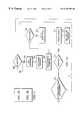
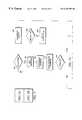
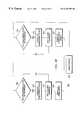
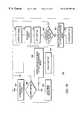
- FIG. 1is a simplified logic block diagram of a representative parallel version of an integrated circuit memory device incorporating a non-volatile memory array and a relatively faster access time memory cache in accordance with the present invention
- FIGS. 2, 2 A, and 2 Bare a logic flow chart of an exemplary memory device read cycle operation in an embodiment of the present invention utilizing a FRAM technology-based non-volatile memory array and an SRAM-based memory for the cache in a “write back” caching scheme;
- FIGS. 3, 3 A, and 3 Bare a corresponding logic flow chart of an exemplary memory device write cycle operation in an embodiment of the present invention corresponding to the embodiment characterized in FIG. 2 utilizing a “write back” caching scheme;
- FIGS. 4, 4 A, and 4 Bare a logic flow chart of an exemplary memory device read cycle operation in an embodiment of the present invention utilizing a FRAM technology-based non-volatile memory array and an SRAM-based memory for the cache in a “write through” caching scheme;
- FIGS. 5, 5 A, and 5 Bare a corresponding logic flow chart of an exemplary memory device write cycle operation in an embodiment of the present invention corresponding to the embodiment characterized in FIG. 4 utilizing a “write through” caching scheme;
- FIGS. 6, 6 A, and 6 Bare a logic flow chart of an exemplary memory device read cycle operation in an embodiment of the present invention utilizing an EEPROM or Flash technology-based non-volatile memory array and an SRAM-based memory for the cache in a “write back” caching scheme;
- FIGS. 7, 7 A, and 7 Bare a corresponding logic flow chart of an exemplary memory device write cycle operation in an embodiment of the present invention corresponding to the embodiment characterized in FIG. 6 utilizing a “write back” caching scheme.
- FIG. 1a simplified logic block diagram of a representative integrated circuit memory device 10 incorporating a non-volatile memory array 12 and a relatively faster access time memory cache 14 in accordance with the present invention is shown. It should be noted that although a parallel memory device 10 has been illustrated, the principles of the present invention are likewise applicable to those incorporating a serial data bus as well as synchronous devices.
- the exemplary memory device 10 illustratedis accessed by means of an external address bus 16 comprising a number of address lines A 0 through A n inclusive.
- the address busis applied to a row address latch 18 as well as a column address latch 20 .
- the row address latch 18 and column address latch 20are operative to respectively maintain a row and column address for accesses to the non-volatile memory array 12 .
- the output of the row address latch 18is supplied directly to a row decoder 22 associated with the non-volatile memory array 12 for accessing a specified row therein as well as to a row address compare block 24 .
- the output of the column address latch 20is supplied to a corresponding column decoder 26 for accessing a specified column of the non-volatile memory array 12 as determined by that portion of the address signal supplied to the address bus 16 maintained in the column address latch 20 .
- the cache 14may be interposed between the column decoder 26 and a number of sense amplifiers 28 bi-directionally coupling the column decoder and the non-volatile memory array 12 .
- the cache 14may comprise a row of SRAM registers for maintaining a last row read (“LRR”) from the non-volatile memory array 12 , which itself may be constructed utilizing FRAM technology memory cells.
- LRRlast row read
- the cache 14may be rendered essentially non-volatile through the use of a pair of FRAM memory cells associated with SRAM memory cells as disclosed in U.S. Pat. No. 4,809,225 assigned to Ramtron International Corporation, the disclosure of which is herein incorporated by this reference.
- An input/output (“I/O”) decoder (or controller) 30is coupled to an output of the row address compare block 24 and is bi-directionally coupled to the cache 14 .
- the I/O decoder 30presents an external “Ready”(or “Not Ready” signal, either of which might be active “high” or active “low”) on line 32 .
- Data output from, (i.e. “Q”) or data to be written to, (i.e. “D”) the memory device 10is handled by means of an input/output (“I/O”) bus 34 which may comprise any number of bi-directional signal lines I/O 0 through I/O N . In a serial implementation the “Q” and “D” signals would be separate outputs and inputs respectively.
- An externally supplied chip select (“CS”)signal on line 38 , write enable (“WE”) signal on line 40 and output enable (“OE”) signal on line 42are also supplied to the memory device 10 through the I/O decoder 30 .
- an external clock signal (“CLK”)may be supplied on an optional clock line 36 .
- datais read from and written to the non-volatile memory array 12 through the cache 14 .
- an address bus 16(A 0 -A n ), the I/O bus 34 , chip select (or chip enable) line 38 (“CS” or “CE”), a write enable line 40 (“WE”), an output enable line 42 (“OE”) and a Ready line 32 .
- the row address compare block 24 and Ready line 32signal the user when data is present in the row register, or cache 14 , and a fast access is practicable.
- This functionmay be implemented externally (by the user) but inclusion as a portion of the memory device 10 has certain advantages.
- Alternative access and control schemesi.e. multiplexed addresses, burst counters, read only, common I/O, etc. are also within the contemplation of the present invention.
- FRAM memory cellsfor the non-volatile memory array 12 supports a much faster write cycle then does either Flash or EEPROM and therefore both “write through” and “write back” caching mechanisms might be utilized depending on the particular application.
- the following discussiondescribes the logical control for a memory device 10 for each of these technologies in a single bank implementation, although it should be noted that the principles of the present invention are likewise applicable to multiple non-volatile memory array 12 banks within a given memory device 10 .
- FIG. 2the operation of a particular implementation of a memory device 10 in accordance with the present invention is shown for a read operation utilizing an FRAM memory cell based non-volatile memory array 12 in a write back caching scheme.
- a write back operationis contemplated wherein all accesses to the memory device 10 are made via the SRAM cache 14 .
- the contents of the cache 14is only written to the non-volatile memory array 12 on a row “miss” or if the chip select (or chip enable “CE”) line 38 transitions to an inactive state (i.e. the memory device 10 is deactivated).
- the control logicmust, therefore, know if the cache 14 has been written for which the embodiment of the present invention shown sets a ““dirty” bit” if a write has occurred.
- the SRAM row cache 14also allows for reads from the cache 14 while a precharge cycle is completed.
- the current implementation of FRAM memory cell based memoriesinverts the data in the memory cell to determine the state. The data is written back to the cell during the precharge cycle. If the previous cycle had been a read “miss”, the precharge cycle could be in progress. Accesses to the non-volatile memory array 12 cannot be performed until the cycle is complete. In future implementations of ferroelectric memories this may no longer be necessary and, therefore, these delays could be eliminated.
- Thiswill reduce the cycle time in applications where reads are either local or sequential (cache “hit”s).
- the memory device 10 operationbegins with the chip enable (or chip select) line 38 going active (either active “high” or active “low” as a design choice) and depends on the state of the cache 14 (“dirty” or “clean”) and the operation preceding the cycle.
- the process 100begins with the memory device 10 in a standby mode until the CE line 38 becomes active at decision step 102 .
- the address on the address bus 16is detected at step 104 and latched at step 106 .
- a read or write cycleis determined by the state of write enable line 40 at decision step 142 following a row address compare step 108 . If at decision step 142 the WE line 40 is active, the process 100 proceeds to a write cycle as will be more fully described hereinafter with respect to FIG. 3 .
- the read cycleis preceded by a page (row) detect operation at decision step 110 to determine if the data is in the cache 14 (row register). If the address is in the cache (a read “hit”), the Ready line 32 is asserted at step 112 , the column address is acquired at step 114 , the appropriate data is output at step 116 , the Ready signal on line 32 is de-asserted at step 118 (after a predetermined delay). At this point the memory device 10 will wait for a new valid address or a transition of the chip enable line 38 to an inactive state at decision step 120 . If the chip enable line 38 has gone inactive, the “dirty” bit is checked at decision step 122 .
- the cache 14is “dirty”, it is written back at step 124 to the non-volatile memory array 12 (if a precharge cycle is in progress, it must complete before the write back begins), and the “dirty” bit is cleared at step 126 . This maintains coherency between the contents of the cache 14 and the non-volatile memory array 12 should a power down cycle occur before the CE line 38 becomes active again.
- the memory device 10then waits for the chip enable line 38 to become active at decision step 102 . If the chip enable line 38 remains active, the memory device 10 waits for a valid address at step 104 .
- a read “miss”the memory device 10 again remains in standby until CE becomes active at decision step 102 .
- the addressis detected at step 104 and latched at step 106 .
- a read or write cycleis determined by the state of write enable line 40 as previously described.
- the read cycleis preceded by a page (row) detect at decision step 110 to determine if the data is in the cache 14 . Since the address is not in the cache 14 (a read “miss”), it must be determined if a precharge cycle is in progress at decision step 128 .
- the precharge cycleis completed at step 130 , a new row is loaded in the cache 138 , the Ready line 32 is asserted at step 112 , the column address is acquired at step 114 , the precharge cycle is initiated at step 140 in parallel, the data is output at step 116 , the Ready line 32 is de-asserted at step 118 after a specified delay, and the memory device waits for a CE line 38 transition at step 120 or a valid address at step 104 . If the CE line 38 transitions, it is handled as previously described with respect to a read “hit”. If a precharge cycle at decision step 128 is not in progress, the “dirty” bit is checked at decision step 132 to see if the cache 14 had been previously written.
- the cache 14is loaded at step 138 and the process 100 proceeds as previously described.
- the cache 14is “dirty”
- the contents of the cache 14are written back to the non-volatile memory array 12 at step 134 (full cycle including precharge)
- the “dirty” bitis cleared at step 136
- the cache 14is loaded at step 138
- the Ready line 32is asserted at step 112 and the process 100 proceeds as hereinbefore described.
- a write cycle process 200is shown.
- the memory device 10In a write “hit” mode of operation, the memory device 10 is in standby until CE line 38 becomes active at decision step 202 .
- the addressis detected at step 204 and latched at step 206 .
- a read or write cycleis determined by the state of the write enable line 40 , and if it is not active at decision step 210 , a read cycle is entered at step 212 .
- the write cycleis preceded by a page detect operation at a row address compare step 208 . If the address is in the cache 14 at decision step 214 (i.e.
- the Ready line 32is asserted at step 216 , the column address is acquired at step 218 , the data is written to the cache 14 at step 220 , the Ready line 32 is de-asserted at step 222 and the “dirty” bit is set at step 224 .
- the memory device 10will wait for a new valid address or for the chip enable line 38 to transition to an inactive state at decision step 226 . If the chip enable line becomes inactive, the contents of the cache 14 are written back to the non-volatile memory array 12 at step 228 . (if a precharge cycle is in progress it must complete before the write back begins), and the “dirty” bit is cleared at step 230 and process 200 proceeds as previously described with respect to a Read Cycle.
- the memory device 10waits for an active chip enable at decision step 202 and a valid address at step 204 .
- a write cycleis determined by the state of write enable line 40 .
- the addressis latched at step 206 and compared at step 208 . If the address is not in the cache 14 , it must then be determined if a precharge cycle is in progress at decision step 232 . If the precharge cycle is in progress, it must be allowed to complete at step 234 before loading the cache 14 at step 242 , the Ready line 32 is asserted at step 216 and the process flow 200 completes as previously described. If a precharge is not in progress, the “dirty” bit is checked at step 236 .
- the cache 14is “clean”, the new row is loaded into the cache 14 at step 242 , the Ready line 32 is asserted at step 216 and the process 200 completes as described. If the “dirty” bit is set at decision step 236 , the contents of the cache 14 are written back to the non-volatile memory array 12 at step 238 and the process 200 completes as previously described.
- Non-volatile memory devices utilizing FRAM memory cellsmay benefit some applications using a write through mechanism.
- the writes in this casewill go directly to the non-volatile memory array 12 or to the cache 14 and the non-volatile memory array 12 in the event of a cache “hit”.
- the control in this instanceis similar to that of the previously described write back case except there is no analogous write “hit”. Writes to the non-volatile memory array 12 will always require the access time of the FRAM array.
- a read process 300is shown.
- a read “hit”the memory device 10 is in standby until CE line 38 becomes active at decision step 302 .
- the addressis detected at step 304 and latched at step 310 .
- a read or write cycleis determined by the state of the write enable line 40 at decision step 306 , and if it is active, then the process 300 proceeds to a write cycle at step 308 .
- the read cycleis preceded by a page (row) detect at step 312 to see if the data is in the cache 14 .
- the Ready line 32is asserted at step 316 , the column address is acquired at step 318 , the data is output on I/O bus 34 at step 320 and the Ready line is de-asserted at step 322 (after a predetermined delay).
- the memory device 10then waits for an active CE line 38 at decision step 302 and a valid address at step 304 .
- a read “miss” operationthe memory device 10 will remain in standby until the CE line 38 becomes active at decision step 302 .
- the addressis detected at step 304 and latched at step 310 as before.
- a read or write cycleis determined by the state of the write enable line 40 .
- the read cycleis preceded by a page (row) detect at decision step 314 to determine if the data is in the cache 14 . Since the data is not in the cache in the case of a read miss, it must be determined if a precharge cycle is in progress at decision step 324 .
- the precharge cycleis completed, a new row is loaded in the cache 14 at step 328 , the Ready line 32 is asserted at step 316 , the column address is acquired at step 318 , the precharge cycle is initiated at step 330 in parallel, the data is output at step 320 , the Ready line 32 is de-asserted at step 322 (following a predetermined delay) and the memory device 10 again waits for the CE line 38 to become active at decision step 302 (if CE is active for another valid address) followed by a valid address at step 304 .
- a write process 400 for a write through mode of operationis shown.
- Writesare written to the non-volatile memory array 12 directly and begin with an active chip enable line 38 at decision step 402 .
- the addressis detected at step 404 and latched at step 410 . If the write enable line 40 is not active at decision step 406 , then a read cycle is initiated at step 408 .
- the row addressis compared at step 412 to determine if the address is in the cache 14 . If the address is in the cache 14 (a row hit) at decision step 414 , it must then be determined if a precharge cycle is in progress at decision step 416 .
- the column addressis acquired at step 420 , the data is written to the cache 14 and the non-volatile memory array 12 simultaneously at step 422 , the Ready line 32 is asserted at step 424 after the access time requirement is met, and the Ready line is de-asserted at step 426 after a specified delay.
- the memory device 10then waits for an active chip enable at decision step 402 and a valid address at step 404 .
- step 414If the address is not in the cache 14 at decision step 414 (a row miss), it is determined if a precharge cycle is in progress at decision step 428 and, if so, it completes at step 430 , the column address is acquired at step 432 , the data is written to the non-volatile memory array only at step 434 (a write through) and the process 400 continues as previously described.
- a memory device 10 with a direct mapped row cache 14(i.e. an SRAM Row Register) coupled with either an EEPROM or Flash non-volatile memory array 12 is similar to a memory device 10 utilizing a FRAM memory cell memory array 12 as described with respect to FIGS. 2-5 inclusive, except that the write mechanisms and write speeds are very much different.
- a read process 500 for a write through caching system utilizing EEPROM, Flash or similar technologies for the non-volatile memory array 12is shown.
- the memory device 10will remain in standby until the CE line 38 becomes active at decision step 502 .
- the addressis detected at step 504 and latched at step 506 as before.
- a read or write cycleis determined by the state of the write enable line 40 at decision step 510 and if it is active, the process 500 proceeds to a write cycle at step 512 .
- the read cycleis preceded by a page (row) detect at step 508 to see if the data is in the cache 14 (row register).
- the memory device 10will wait for a new valid address or a transition of the chip enable line 38 to an inactive state. If the chip enable line 38 has transitioned to an inactive state at decision step 524 , the “dirty” bit is checked at decision step 526 .
- the cache 14is “dirty”, it is written back at step 528 to the EEPROM/Flash non-volatile memory array 12 , and the “dirty” bit is cleared at step 530 . This maintains coherency should a power down cycle occur before the CE line 38 becomes active again.
- the memory device 10then waits for the chip enable line 38 to become active at decision step 502 . If the chip enable line 38 remains active, the memory device 10 waits for a valid address at step 504 .
- a read miss operationthe memory device 10 will remain in standby until the CE line 38 becomes active at decision step 502 , the address is detected at step 504 and latched at step 506 .
- a read or write cycleis determined by the state of the write enable line 40 .
- the read cycleis preceded by a page (row) detect step 508 to determine if the data is in the cache 14 at decision step 514 . Since the address is not in the cache 14 (a read miss), it must be determined if a write cycle is in progress at decision step 532 .
- the write cycleis completed at step 534 , a new row is loaded in the cache 14 at step 542 , the Ready line 32 is asserted at step 516 , the column address is acquired at step 518 , the data is output at step 520 , the Ready line 32 is de-asserted at step 522 after a predetermined delay, and the memory device 10 waits for a CE line 38 transition at step 524 or (if CE line 38 is active) a valid address at step 504 . If the CE line 38 transitions, it is handled as previously described.
- the “dirty” bitis checked at decision step 536 to determine if the cache 14 had been written previously. If the cache 14 is “clean”, the cache 14 is loaded at step 542 and the process 500 completes as aforedescribed.
- the cache 14is “dirty”, the contents of the cache 14 are written back to the EEPROM/Flash non-volatile memory array 12 at step 538 , the “dirty” bit is cleared at step 540 , the write cycle completes at step 534 , the cache is loaded at step 542 , the Ready line 32 is asserted at step 516 and the memory device 10 returns to wait for an active CE line at decision step 502 and a valid address at step 504 .
- a write process 600is shown.
- the memory device 10In a write “hit” mode of operation, the memory device 10 remains in standby until the CE line 38 becomes active at decision step 602 .
- the addressis detected at step 504 and latched at step 606 .
- a read or write cycleis determined by the state of write enable line 40 at decision step 610 , and if it is not active, a read cycle is entered at step 612 .
- the write cycleis preceded by a page detect at step 608 .
- the memory device 10will wait for a new valid address at step 604 or for the chip enable line 38 to transition to an inactive state. If the chip enable line 38 becomes inactive, the contents of the cache 14 are written back to the EEPROM/Flash non-volatile memory array at step 628 , the “dirty” bit is cleared at step 630 and the process 600 returns to wait for an active CE line 38 .
- the memory device 10again waits for an active chip enable line 38 at decision step 602 and a valid address at step 604 .
- the write cycleis determined by the state of the write enable line 40 .
- the addressis latched at step 606 and compared at step 608 . If the address is not in the cache 14 , it must be determined if a write cycle is in progress at decision step 632 . If the write cycle is in progress, it must complete at step 634 before loading the cache 14 at step 642 , the Ready line 32 is asserted at step 616 and the process 600 proceeds as described above. If a write cycle is not in progress, the “dirty” bit is checked at step 636 .
- the cache 14is “clean”, the new row is loaded into the cache 14 at step 642 , the Ready line 32 is asserted at step 616 and the process 600 proceeds as previously described. If the “dirty” bit is set at decision step 636 , the contents of the cache 14 are written back to the EEPROM/Flash non-volatile memory array at step 638 , the write cycle is completed at step 634 , the Ready line 32 is asserted at step 616 and the process 600 proceeds as described above.
- a non-volatile memory arrayis cached by use of a non-volatile memory-based cache.
- asynchronous parallel memory devicehas been illustrated and described herein, the principles of the present invention are likewise applicable to serial and synchronous memory device architectures as well.
Landscapes
- Engineering & Computer Science (AREA)
- Theoretical Computer Science (AREA)
- Computer Hardware Design (AREA)
- Physics & Mathematics (AREA)
- General Engineering & Computer Science (AREA)
- General Physics & Mathematics (AREA)
- Memory System Of A Hierarchy Structure (AREA)
- Dram (AREA)
Abstract
Description
Claims (20)
Priority Applications (2)
| Application Number | Priority Date | Filing Date | Title |
|---|---|---|---|
| US09/021,132US6263398B1 (en) | 1998-02-10 | 1998-02-10 | Integrated circuit memory device incorporating a non-volatile memory array and a relatively faster access time memory cache |
| US09/864,458US20010025333A1 (en) | 1998-02-10 | 2001-05-24 | Integrated circuit memory device incorporating a non-volatile memory array and a relatively faster access time memory cache |
Applications Claiming Priority (1)
| Application Number | Priority Date | Filing Date | Title |
|---|---|---|---|
| US09/021,132US6263398B1 (en) | 1998-02-10 | 1998-02-10 | Integrated circuit memory device incorporating a non-volatile memory array and a relatively faster access time memory cache |
Related Child Applications (1)
| Application Number | Title | Priority Date | Filing Date |
|---|---|---|---|
| US09/864,458ContinuationUS20010025333A1 (en) | 1998-02-10 | 2001-05-24 | Integrated circuit memory device incorporating a non-volatile memory array and a relatively faster access time memory cache |
Publications (1)
| Publication Number | Publication Date |
|---|---|
| US6263398B1true US6263398B1 (en) | 2001-07-17 |
Family
ID=21802518
Family Applications (2)
| Application Number | Title | Priority Date | Filing Date |
|---|---|---|---|
| US09/021,132Expired - LifetimeUS6263398B1 (en) | 1998-02-10 | 1998-02-10 | Integrated circuit memory device incorporating a non-volatile memory array and a relatively faster access time memory cache |
| US09/864,458AbandonedUS20010025333A1 (en) | 1998-02-10 | 2001-05-24 | Integrated circuit memory device incorporating a non-volatile memory array and a relatively faster access time memory cache |
Family Applications After (1)
| Application Number | Title | Priority Date | Filing Date |
|---|---|---|---|
| US09/864,458AbandonedUS20010025333A1 (en) | 1998-02-10 | 2001-05-24 | Integrated circuit memory device incorporating a non-volatile memory array and a relatively faster access time memory cache |
Country Status (1)
| Country | Link |
|---|---|
| US (2) | US6263398B1 (en) |
Cited By (27)
| Publication number | Priority date | Publication date | Assignee | Title |
|---|---|---|---|---|
| WO2002077824A1 (en)* | 2001-03-26 | 2002-10-03 | M-Systems Flash Disk Pioneers Ltd. | Using volatile memory to buffer non-volatile memory |
| US6545891B1 (en) | 2000-08-14 | 2003-04-08 | Matrix Semiconductor, Inc. | Modular memory device |
| US20030147269A1 (en)* | 2002-02-01 | 2003-08-07 | Toshiyuki Nishihara | Memory device and memory system using same |
| US6622243B1 (en)* | 1999-11-19 | 2003-09-16 | Intel Corporation | Method for securing CMOS configuration information in non-volatile memory |
| US6707702B1 (en) | 2002-11-13 | 2004-03-16 | Texas Instruments Incorporated | Volatile memory with non-volatile ferroelectric capacitors |
| US6711043B2 (en) | 2000-08-14 | 2004-03-23 | Matrix Semiconductor, Inc. | Three-dimensional memory cache system |
| US20040125644A1 (en)* | 2002-12-31 | 2004-07-01 | Katsuo Komatsuzaki | Multiple bit memory cells and methods for reading non-volatile data |
| US6765813B2 (en) | 2000-08-14 | 2004-07-20 | Matrix Semiconductor, Inc. | Integrated systems using vertically-stacked three-dimensional memory cells |
| GB2397408A (en)* | 2003-01-15 | 2004-07-21 | Agilent Technologies Inc | EEPROM emulation in an optical transceiver |
| US6768661B2 (en) | 2002-06-27 | 2004-07-27 | Matrix Semiconductor, Inc. | Multiple-mode memory and method for forming same |
| US6798599B2 (en) | 2001-01-29 | 2004-09-28 | Seagate Technology Llc | Disc storage system employing non-volatile magnetoresistive random access memory |
| US20040225829A1 (en)* | 2003-05-09 | 2004-11-11 | Satoru Akiyama | Semiconductor device |
| US6836816B2 (en)* | 2001-03-28 | 2004-12-28 | Intel Corporation | Flash memory low-latency cache |
| US20050013181A1 (en)* | 2003-07-17 | 2005-01-20 | Adelmann Todd C. | Assisted memory device with integrated cache |
| US20050091547A1 (en)* | 2003-10-27 | 2005-04-28 | Paul Hanrieder | High speed non-volatile electronic memory configuration |
| US20050195635A1 (en)* | 2004-03-08 | 2005-09-08 | Conley Kevin M. | Flash controller cache architecture |
| US6947310B1 (en) | 2004-05-13 | 2005-09-20 | Texas Instruments Incorporated | Ferroelectric latch |
| US20050251617A1 (en)* | 2004-05-07 | 2005-11-10 | Sinclair Alan W | Hybrid non-volatile memory system |
| US20060136656A1 (en)* | 2004-12-21 | 2006-06-22 | Conley Kevin M | System and method for use of on-chip non-volatile memory write cache |
| US20060168418A1 (en)* | 2005-01-25 | 2006-07-27 | Adusumilli Vijaya P | Simultaneous pipelined read with dual level cache for improved system performance using flash technology |
| US20070028034A1 (en)* | 2005-07-29 | 2007-02-01 | Sony Corporation | Computer system |
| US20100274962A1 (en)* | 2009-04-26 | 2010-10-28 | Sandisk Il Ltd. | Method and apparatus for implementing a caching policy for non-volatile memory |
| US8180981B2 (en) | 2009-05-15 | 2012-05-15 | Oracle America, Inc. | Cache coherent support for flash in a memory hierarchy |
| USRE44052E1 (en)* | 2001-06-04 | 2013-03-05 | Samsung Electronics Co., Ltd. | Flash memory management method |
| US20130173864A1 (en)* | 2012-01-04 | 2013-07-04 | Elpida Memory, Inc. | Semiconductor device including row cache register |
| US9852315B2 (en)* | 2011-04-29 | 2017-12-26 | Altera Corporation | Systems and methods for detecting and mitigating programmable logic device tampering |
| TWI644324B (en)* | 2016-03-10 | 2018-12-11 | 美光科技公司 | Parallel access techniques within memory sections through section independence |
Families Citing this family (11)
| Publication number | Priority date | Publication date | Assignee | Title |
|---|---|---|---|---|
| US7389384B2 (en)* | 2002-04-30 | 2008-06-17 | Dsp Group Switzerland Ag | Apparatus and method for fetching data from memory |
| AU2002353406A1 (en)* | 2002-12-27 | 2004-07-22 | Solid State System Co., Ltd. | Nonvolatile memory unit with specific cache |
| DE10317147A1 (en)* | 2003-04-14 | 2004-10-28 | Nec Electronics (Europe) Gmbh | Secure storage system with flash memories and cache memory |
| US20050050261A1 (en)* | 2003-08-27 | 2005-03-03 | Thomas Roehr | High density flash memory with high speed cache data interface |
| JP2005301591A (en)* | 2004-04-09 | 2005-10-27 | Toshiba Corp | Device having nonvolatile memory and memory controller |
| JP2007220168A (en)* | 2006-02-14 | 2007-08-30 | Matsushita Electric Ind Co Ltd | Semiconductor memory device |
| US20110202709A1 (en)* | 2008-03-19 | 2011-08-18 | Rambus Inc. | Optimizing storage of common patterns in flash memory |
| US8458404B1 (en)* | 2008-08-14 | 2013-06-04 | Marvell International Ltd. | Programmable cache access protocol to optimize power consumption and performance |
| US8327076B2 (en)* | 2009-05-13 | 2012-12-04 | Seagate Technology Llc | Systems and methods of tiered caching |
| JP2012038385A (en)* | 2010-08-06 | 2012-02-23 | Renesas Electronics Corp | Data processor |
| JP6072661B2 (en)* | 2013-09-30 | 2017-02-01 | ルネサスエレクトロニクス株式会社 | Data processing device, microcontroller, and semiconductor device |
Citations (8)
| Publication number | Priority date | Publication date | Assignee | Title |
|---|---|---|---|---|
| US4809225A (en) | 1987-07-02 | 1989-02-28 | Ramtron Corporation | Memory cell with volatile and non-volatile portions having ferroelectric capacitors |
| US5307470A (en)* | 1988-11-25 | 1994-04-26 | Nec Corporation | Microcomputer having EEPROM provided with detector for detecting data write request issued before data write operation responsive to preceding data write request is completed |
| US5682344A (en) | 1995-09-11 | 1997-10-28 | Micron Technology, Inc. | Destructive read protection using address blocking technique |
| US5699317A (en)* | 1992-01-22 | 1997-12-16 | Ramtron International Corporation | Enhanced DRAM with all reads from on-chip cache and all writers to memory array |
| US5737748A (en)* | 1995-03-15 | 1998-04-07 | Texas Instruments Incorporated | Microprocessor unit having a first level write-through cache memory and a smaller second-level write-back cache memory |
| US5802583A (en)* | 1996-10-30 | 1998-09-01 | Ramtron International Corporation | Sysyem and method providing selective write protection for individual blocks of memory in a non-volatile memory device |
| US5860113A (en)* | 1996-06-03 | 1999-01-12 | Opti Inc. | System for using a dirty bit with a cache memory |
| US6012140A (en)* | 1996-09-26 | 2000-01-04 | U.S. Philips Corporation | Processing system, processing unit, memory and compiling method |
- 1998
- 1998-02-10USUS09/021,132patent/US6263398B1/ennot_activeExpired - Lifetime
- 2001
- 2001-05-24USUS09/864,458patent/US20010025333A1/ennot_activeAbandoned
Patent Citations (9)
| Publication number | Priority date | Publication date | Assignee | Title |
|---|---|---|---|---|
| US4809225A (en) | 1987-07-02 | 1989-02-28 | Ramtron Corporation | Memory cell with volatile and non-volatile portions having ferroelectric capacitors |
| US5307470A (en)* | 1988-11-25 | 1994-04-26 | Nec Corporation | Microcomputer having EEPROM provided with detector for detecting data write request issued before data write operation responsive to preceding data write request is completed |
| US5699317A (en)* | 1992-01-22 | 1997-12-16 | Ramtron International Corporation | Enhanced DRAM with all reads from on-chip cache and all writers to memory array |
| US5721862A (en)* | 1992-01-22 | 1998-02-24 | Ramtron International Corporation | Enhanced DRAM with single row SRAM cache for all device read operations |
| US5737748A (en)* | 1995-03-15 | 1998-04-07 | Texas Instruments Incorporated | Microprocessor unit having a first level write-through cache memory and a smaller second-level write-back cache memory |
| US5682344A (en) | 1995-09-11 | 1997-10-28 | Micron Technology, Inc. | Destructive read protection using address blocking technique |
| US5860113A (en)* | 1996-06-03 | 1999-01-12 | Opti Inc. | System for using a dirty bit with a cache memory |
| US6012140A (en)* | 1996-09-26 | 2000-01-04 | U.S. Philips Corporation | Processing system, processing unit, memory and compiling method |
| US5802583A (en)* | 1996-10-30 | 1998-09-01 | Ramtron International Corporation | Sysyem and method providing selective write protection for individual blocks of memory in a non-volatile memory device |
Cited By (55)
| Publication number | Priority date | Publication date | Assignee | Title |
|---|---|---|---|---|
| US6622243B1 (en)* | 1999-11-19 | 2003-09-16 | Intel Corporation | Method for securing CMOS configuration information in non-volatile memory |
| US6711043B2 (en) | 2000-08-14 | 2004-03-23 | Matrix Semiconductor, Inc. | Three-dimensional memory cache system |
| US6765813B2 (en) | 2000-08-14 | 2004-07-20 | Matrix Semiconductor, Inc. | Integrated systems using vertically-stacked three-dimensional memory cells |
| US20030151959A1 (en)* | 2000-08-14 | 2003-08-14 | Matrix Semiconductor, Inc. | Modular memory device |
| US6545891B1 (en) | 2000-08-14 | 2003-04-08 | Matrix Semiconductor, Inc. | Modular memory device |
| US6867992B2 (en) | 2000-08-14 | 2005-03-15 | Matrix Semiconductor, Inc. | Modular memory device |
| US6798599B2 (en) | 2001-01-29 | 2004-09-28 | Seagate Technology Llc | Disc storage system employing non-volatile magnetoresistive random access memory |
| WO2002077824A1 (en)* | 2001-03-26 | 2002-10-03 | M-Systems Flash Disk Pioneers Ltd. | Using volatile memory to buffer non-volatile memory |
| US6836816B2 (en)* | 2001-03-28 | 2004-12-28 | Intel Corporation | Flash memory low-latency cache |
| USRE46404E1 (en) | 2001-06-04 | 2017-05-16 | Samsung Electronics Co., Ltd. | Flash memory management method |
| USRE44052E1 (en)* | 2001-06-04 | 2013-03-05 | Samsung Electronics Co., Ltd. | Flash memory management method |
| USRE45577E1 (en)* | 2001-06-04 | 2015-06-23 | Samsung Electronics Co., Ltd. | Method of writing to a flash memory including data blocks and log blocks |
| USRE45222E1 (en)* | 2001-06-04 | 2014-10-28 | Samsung Electronics Co., Ltd. | Method of writing of writing to a flash memory including data blocks and log blocks, using a logical address having a block address portion and page identifying portion, a block address table and a page table |
| US6771531B2 (en)* | 2002-02-01 | 2004-08-03 | Sony Corporation | Memory device and memory system using same |
| US20030147269A1 (en)* | 2002-02-01 | 2003-08-07 | Toshiyuki Nishihara | Memory device and memory system using same |
| US6768661B2 (en) | 2002-06-27 | 2004-07-27 | Matrix Semiconductor, Inc. | Multiple-mode memory and method for forming same |
| US6839262B2 (en) | 2002-06-27 | 2005-01-04 | Matrix Semiconductor, Inc. | Multiple-mode memory and method for forming same |
| US20040184296A1 (en)* | 2002-06-27 | 2004-09-23 | Matrix Semiconductor, Inc. | Multiple-mode memory and method for forming same |
| US6707702B1 (en) | 2002-11-13 | 2004-03-16 | Texas Instruments Incorporated | Volatile memory with non-volatile ferroelectric capacitors |
| US6944042B2 (en) | 2002-12-31 | 2005-09-13 | Texas Instruments Incorporated | Multiple bit memory cells and methods for reading non-volatile data |
| US20040125644A1 (en)* | 2002-12-31 | 2004-07-01 | Katsuo Komatsuzaki | Multiple bit memory cells and methods for reading non-volatile data |
| GB2397408A (en)* | 2003-01-15 | 2004-07-21 | Agilent Technologies Inc | EEPROM emulation in an optical transceiver |
| GB2397408B (en)* | 2003-01-15 | 2005-11-16 | Agilent Technologies Inc | Transceiver |
| US7636808B2 (en)* | 2003-05-09 | 2009-12-22 | Hitachi, Ltd. | Semiconductor device |
| US20040225829A1 (en)* | 2003-05-09 | 2004-11-11 | Satoru Akiyama | Semiconductor device |
| US20050013181A1 (en)* | 2003-07-17 | 2005-01-20 | Adelmann Todd C. | Assisted memory device with integrated cache |
| US7315951B2 (en)* | 2003-10-27 | 2008-01-01 | Nortel Networks Corporation | High speed non-volatile electronic memory configuration |
| US20050091547A1 (en)* | 2003-10-27 | 2005-04-28 | Paul Hanrieder | High speed non-volatile electronic memory configuration |
| US9678877B2 (en) | 2004-03-08 | 2017-06-13 | Sandisk Technologies Llc | Flash controller cache architecture |
| US7173863B2 (en) | 2004-03-08 | 2007-02-06 | Sandisk Corporation | Flash controller cache architecture |
| US20070143545A1 (en)* | 2004-03-08 | 2007-06-21 | Conley Kevin M | Flash Controller Cache Architecture |
| US7408834B2 (en) | 2004-03-08 | 2008-08-05 | Sandisck Corporation Llp | Flash controller cache architecture |
| US20080250202A1 (en)* | 2004-03-08 | 2008-10-09 | Sandisk Corporation | Flash controller cache architecture |
| US20050195635A1 (en)* | 2004-03-08 | 2005-09-08 | Conley Kevin M. | Flash controller cache architecture |
| US20100023681A1 (en)* | 2004-05-07 | 2010-01-28 | Alan Welsh Sinclair | Hybrid Non-Volatile Memory System |
| US20050251617A1 (en)* | 2004-05-07 | 2005-11-10 | Sinclair Alan W | Hybrid non-volatile memory system |
| US6947310B1 (en) | 2004-05-13 | 2005-09-20 | Texas Instruments Incorporated | Ferroelectric latch |
| US20060136656A1 (en)* | 2004-12-21 | 2006-06-22 | Conley Kevin M | System and method for use of on-chip non-volatile memory write cache |
| US7882299B2 (en) | 2004-12-21 | 2011-02-01 | Sandisk Corporation | System and method for use of on-chip non-volatile memory write cache |
| US20060168418A1 (en)* | 2005-01-25 | 2006-07-27 | Adusumilli Vijaya P | Simultaneous pipelined read with dual level cache for improved system performance using flash technology |
| US7877566B2 (en) | 2005-01-25 | 2011-01-25 | Atmel Corporation | Simultaneous pipelined read with multiple level cache for improved system performance using flash technology |
| US20070028034A1 (en)* | 2005-07-29 | 2007-02-01 | Sony Corporation | Computer system |
| US7571282B2 (en)* | 2005-07-29 | 2009-08-04 | Sony Corporation | Computer system having a flash memory storage device |
| US8103822B2 (en)* | 2009-04-26 | 2012-01-24 | Sandisk Il Ltd. | Method and apparatus for implementing a caching policy for non-volatile memory |
| US20100274962A1 (en)* | 2009-04-26 | 2010-10-28 | Sandisk Il Ltd. | Method and apparatus for implementing a caching policy for non-volatile memory |
| US8180981B2 (en) | 2009-05-15 | 2012-05-15 | Oracle America, Inc. | Cache coherent support for flash in a memory hierarchy |
| US10592699B2 (en) | 2011-04-29 | 2020-03-17 | Altera Corporation | Systems and methods for detecting and mitigating of programmable logic device tampering |
| US9852315B2 (en)* | 2011-04-29 | 2017-12-26 | Altera Corporation | Systems and methods for detecting and mitigating programmable logic device tampering |
| US11436382B2 (en) | 2011-04-29 | 2022-09-06 | Altera Corporation | Systems and methods for detecting and mitigating programmable logic device tampering |
| US20130173864A1 (en)* | 2012-01-04 | 2013-07-04 | Elpida Memory, Inc. | Semiconductor device including row cache register |
| TWI644324B (en)* | 2016-03-10 | 2018-12-11 | 美光科技公司 | Parallel access techniques within memory sections through section independence |
| US10373665B2 (en)* | 2016-03-10 | 2019-08-06 | Micron Technology, Inc. | Parallel access techniques within memory sections through section independence |
| US10388352B2 (en) | 2016-03-10 | 2019-08-20 | Micron Technology, Inc. | Parallel access techniques within memory sections through section independence |
| US10770126B2 (en) | 2016-03-10 | 2020-09-08 | Micron Technology, Inc. | Parallel access techniques within memory sections through section independence |
| US11501814B2 (en) | 2016-03-10 | 2022-11-15 | Micron Technology, Inc. | Parallel access techniques within memory sections through section independence |
Also Published As
| Publication number | Publication date |
|---|---|
| US20010025333A1 (en) | 2001-09-27 |
Similar Documents
| Publication | Publication Date | Title |
|---|---|---|
| US6263398B1 (en) | Integrated circuit memory device incorporating a non-volatile memory array and a relatively faster access time memory cache | |
| US11024367B2 (en) | Memory with on-die data transfer | |
| US6665209B2 (en) | Semiconductor memory apparatus, semiconductor apparatus, data processing apparatus and computer system | |
| US5025421A (en) | Single port dual RAM | |
| US6484246B2 (en) | High-speed random access semiconductor memory device | |
| JP3304413B2 (en) | Semiconductor storage device | |
| US6546461B1 (en) | Multi-port cache memory devices and FIFO memory devices having multi-port cache memory devices therein | |
| US6134180A (en) | Synchronous burst semiconductor memory device | |
| JP3280704B2 (en) | Semiconductor storage device | |
| CA2313954A1 (en) | High speed dram architecture with uniform latency | |
| US7464231B2 (en) | Method for self-timed data ordering for multi-data rate memories | |
| US20080031067A1 (en) | Block erase for volatile memory | |
| US6175533B1 (en) | Multi-port memory cell with preset | |
| US20090106488A1 (en) | Static random access memory (sram) compatible, high availability memory array and method employing synchronous dynamic random access memory (dram) in conjunction with a data cache and separate read and write registers and tag blocks | |
| JP2004334996A (en) | Semiconductor device | |
| US7093047B2 (en) | Integrated circuit memory devices having clock signal arbitration circuits therein and methods of performing clock signal arbitration | |
| JP5189887B2 (en) | Ferroelectric memory device and operation method thereof | |
| US6246603B1 (en) | Circuit and method for substantially preventing imprint effects in a ferroelectric memory device | |
| JP3789998B2 (en) | Memory built-in processor | |
| US7146454B1 (en) | Hiding refresh in 1T-SRAM architecture | |
| US20060190678A1 (en) | Static random access memory (SRAM) compatible, high availability memory array and method employing synchronous dynamic random access memory (DRAM) in conjunction with a single DRAM cache and tag | |
| US5802002A (en) | Cache memory device of DRAM configuration without refresh function | |
| US6456519B1 (en) | Circuit and method for asynchronously accessing a ferroelectric memory device | |
| CN107844430B (en) | memory system and processor system | |
| CN118748031A (en) | Bit line sensing amplifier with bit line-storage node decoupling, storage-computation-in-one memory, and in-situ matrix calculation method |
Legal Events
| Date | Code | Title | Description |
|---|---|---|---|
| AS | Assignment | Owner name:RAMTRON INTERNATIONAL CORPORATION, COLORADO Free format text:ASSIGNMENT OF ASSIGNORS INTEREST;ASSIGNORS:TAYLOR, CRAIG;CARRIGAN, DONALD G.;ALWAIS, MIKE;REEL/FRAME:009118/0395;SIGNING DATES FROM 19980317 TO 19980320 | |
| AS | Assignment | Owner name:RAMTRON INTERNATIONAL CORPORATION, COLORADO Free format text:FIRST AMENDMENT TO PATENT SEC. AGMNT.;ASSIGNOR:NATONAL ELECTRICAL BENEFIT FUND;REEL/FRAME:009756/0085 Effective date:19990115 Owner name:RAMTRON INTERNATIONAL CORPORATION, COLORADO Free format text:FIRST AMENDMENT TO PATENT SEC. AGMNT;ASSIGNOR:NATONAL ELECTRICAL BENEFIT FUND;REEL/FRAME:009756/0085 Effective date:19990115 | |
| STCF | Information on status: patent grant | Free format text:PATENTED CASE | |
| AS | Assignment | Owner name:INFINEON TECHNOLOGIES AG, GERMANY Free format text:SECURITY INTEREST;ASSIGNOR:RAMTRON INTERNATIONAL CORPORATION;REEL/FRAME:012653/0747 Effective date:20020328 | |
| FPAY | Fee payment | Year of fee payment:4 | |
| AS | Assignment | Owner name:RAMTRON INTERNATIONAL CORPORATION, COLORADO Free format text:RELEASE OF SECURITY INTEREST;ASSIGNOR:INFINEON TECHNOLOGIES AG;REEL/FRAME:016976/0575 Effective date:20050704 | |
| AS | Assignment | Owner name:SILICON VALLEY BANK, CALIFORNIA Free format text:SECURITY AGREEMENT;ASSIGNOR:RAMTRON INTERNATIONAL CORPORATION;REEL/FRAME:017105/0174 Effective date:20051017 | |
| FPAY | Fee payment | Year of fee payment:8 | |
| AS | Assignment | Owner name:CYPRESS SEMICONDUCTOR CORPORATION, CALIFORNIA Free format text:ASSIGNMENT OF ASSIGNORS INTEREST;ASSIGNOR:RAMTRON INTERNATIONAL CORPORATION;REEL/FRAME:029408/0437 Effective date:20121203 | |
| FPAY | Fee payment | Year of fee payment:12 | |
| AS | Assignment | Owner name:RAMTRON INTERNATIONAL CORPORATION, COLORADO Free format text:RELEASE;ASSIGNOR:SILICON VALLEY BANK;REEL/FRAME:035257/0406 Effective date:20050915 | |
| AS | Assignment | Owner name:MORGAN STANLEY SENIOR FUNDING, INC., NEW YORK Free format text:SECURITY INTEREST;ASSIGNORS:CYPRESS SEMICONDUCTOR CORPORATION;SPANSION LLC;REEL/FRAME:035240/0429 Effective date:20150312 | |
| AS | Assignment | Owner name:SPANSION LLC, CALIFORNIA Free format text:PARTIAL RELEASE OF SECURITY INTEREST IN PATENTS;ASSIGNOR:MORGAN STANLEY SENIOR FUNDING, INC., AS COLLATERAL AGENT;REEL/FRAME:039708/0001 Effective date:20160811 Owner name:CYPRESS SEMICONDUCTOR CORPORATION, CALIFORNIA Free format text:PARTIAL RELEASE OF SECURITY INTEREST IN PATENTS;ASSIGNOR:MORGAN STANLEY SENIOR FUNDING, INC., AS COLLATERAL AGENT;REEL/FRAME:039708/0001 Effective date:20160811 | |
| AS | Assignment | Owner name:MONTEREY RESEARCH, LLC, CALIFORNIA Free format text:ASSIGNMENT OF ASSIGNORS INTEREST;ASSIGNOR:CYPRESS SEMICONDUCTOR CORPORATION;REEL/FRAME:040911/0238 Effective date:20160811 | |
| AS | Assignment | Owner name:MORGAN STANLEY SENIOR FUNDING, INC., NEW YORK Free format text:CORRECTIVE ASSIGNMENT TO CORRECT THE 8647899 PREVIOUSLY RECORDED ON REEL 035240 FRAME 0429. ASSIGNOR(S) HEREBY CONFIRMS THE SECURITY INTERST;ASSIGNORS:CYPRESS SEMICONDUCTOR CORPORATION;SPANSION LLC;REEL/FRAME:058002/0470 Effective date:20150312 |