US6262918B1 - Space management for managing high capacity nonvolatile memory - Google Patents
Space management for managing high capacity nonvolatile memoryDownload PDFInfo
- Publication number
- US6262918B1 US6262918B1US09/610,545US61054500AUS6262918B1US 6262918 B1US6262918 B1US 6262918B1US 61054500 AUS61054500 AUS 61054500AUS 6262918 B1US6262918 B1US 6262918B1
- Authority
- US
- United States
- Prior art keywords
- block
- nonvolatile memory
- blocks
- super
- erasure
- Prior art date
- Legal status (The legal status is an assumption and is not a legal conclusion. Google has not performed a legal analysis and makes no representation as to the accuracy of the status listed.)
- Expired - Lifetime
Links
Images


Classifications
- G—PHYSICS
- G11—INFORMATION STORAGE
- G11C—STATIC STORES
- G11C8/00—Arrangements for selecting an address in a digital store
- G11C8/12—Group selection circuits, e.g. for memory block selection, chip selection, array selection
- G—PHYSICS
- G06—COMPUTING OR CALCULATING; COUNTING
- G06F—ELECTRIC DIGITAL DATA PROCESSING
- G06F12/00—Accessing, addressing or allocating within memory systems or architectures
- G06F12/02—Addressing or allocation; Relocation
- G06F12/0223—User address space allocation, e.g. contiguous or non contiguous base addressing
- G06F12/023—Free address space management
- G06F12/0238—Memory management in non-volatile memory, e.g. resistive RAM or ferroelectric memory
- G06F12/0246—Memory management in non-volatile memory, e.g. resistive RAM or ferroelectric memory in block erasable memory, e.g. flash memory
- G—PHYSICS
- G11—INFORMATION STORAGE
- G11C—STATIC STORES
- G11C16/00—Erasable programmable read-only memories
- G11C16/02—Erasable programmable read-only memories electrically programmable
- G11C16/04—Erasable programmable read-only memories electrically programmable using variable threshold transistors, e.g. FAMOS
- G—PHYSICS
- G11—INFORMATION STORAGE
- G11C—STATIC STORES
- G11C16/00—Erasable programmable read-only memories
- G11C16/02—Erasable programmable read-only memories electrically programmable
- G11C16/06—Auxiliary circuits, e.g. for writing into memory
- G11C16/10—Programming or data input circuits
- G11C16/14—Circuits for erasing electrically, e.g. erase voltage switching circuits
- G11C16/16—Circuits for erasing electrically, e.g. erase voltage switching circuits for erasing blocks, e.g. arrays, words, groups
- G—PHYSICS
- G06—COMPUTING OR CALCULATING; COUNTING
- G06F—ELECTRIC DIGITAL DATA PROCESSING
- G06F2212/00—Indexing scheme relating to accessing, addressing or allocation within memory systems or architectures
- G06F2212/72—Details relating to flash memory management
- G06F2212/7205—Cleaning, compaction, garbage collection, erase control
- G—PHYSICS
- G06—COMPUTING OR CALCULATING; COUNTING
- G06F—ELECTRIC DIGITAL DATA PROCESSING
- G06F2212/00—Indexing scheme relating to accessing, addressing or allocation within memory systems or architectures
- G06F2212/72—Details relating to flash memory management
- G06F2212/7208—Multiple device management, e.g. distributing data over multiple flash devices
Definitions
- This inventionrelates to the field of digital systems employing non-volatile memory and particularly flash memory as mass storage for computers, digital cameras and the like.
- solid state memoryhas gained popularity for use in replacing mass storage units in various technology areas such as computers, digital cameras, modems and the like.
- solid state memorysuch as flash memory
- Flash memoryis generally provided in the form of semiconductor devices (or chips) with each device made of a large number of transistor memory cells and each cell being individually programmable.
- the programming (or writing) and erasing of such a memory cellis limited to a finite number of erase-write cycles, which basically determines the lifetime of the device.
- an inherent characteristic of flash memory cellsis that they must be erased and verified for successful erase prior to being programmed.
- a hostwrites and reads information to the flash memory devices through a controller device, which is commonly in the form of a semiconductor device. Such information is organized in sectors with each sector including user data information and overhead information and being generally 512 bytes in length.
- the controllerupon receiving sector information from the host, during a host-commanded write operation, writes the information to the flash memory devices in accordance with a predetermined sector organization. While the host may be accessing multiple sectors, each sector is written to the flash devices one at a time.
- a computer (or host) systemIn storing and/or retrieving a data file (data files may be any computer files including commercial software, user program, word processor software document, spread sheet file and the like), a computer (or host) system provides what is referred to as the logical block address indicating the location of where the host believes the data file to exist within the mass storage.
- the host-provided addressmay be in the form of cylinder, head and sector (CHS), which is converted to a logical block address format upon receipt by the controller. The same applies to digital camera applications.
- the controllerthen translates the logical block address (LBA) into a physical block address (PBA) and uses the latter to access the data file within flash memory.
- LBAlogical block address
- PBAphysical block address
- a variety of different algorithmsmay be employed for determining when an erase operation(s) will take place and as a function thereof, where within the flash memory (mass storage) the next available free block is located for storing the data file.
- the space manager unit of the controller deviceperforms this function.
- Information in the nonvolatile memory or flash memoryis stored under the direction of the controller and it is done so in the form of blocks.
- information that is stored in nonvolatile memoryis organized in blocks and each block is uniquely addressable by the controller.
- Each blockis further comprised of multiple sectors with each sector defining 512 bytes of storage space. In some prior art systems, during an erase operation, an entire block is erased whereas in other prior art systems, the sector may be erased.
- Each blockis uniquely addressable for reading and writing information from and to the nonvolatile memory.
- Each sectorincludes information such as data, flags and Error Correction Codes (ECC).
- ECCError Correction Codes
- the address of a block within the nonvolatile memoryis maintained within the respective block for use in reconstructing the addressing or mapping information associated with the nonvolatile memory after a power-down.
- This mapping informationis the contents of a look-up-table maintained in volatile memory, as will now be further described.
- the space manager unit of the controller devicemaintains a table of information regarding the location of the most recent data within the flash memory in addition to the location of information that is considered ‘old’ (information which has been superseded) and not yet erased and/or ‘defective’ (location can not be used for storing information due to some kind of defect) or ‘used’ (currently contains up-to-date information).
- This table of informationis stored and updated in a volatile memory location such as RAM either within or outside of the controller device. Each time information is accessed by the host, the space manager table is used to find out the location of the information that is to be written and/or read from the flash memory devices.
- the problem with prior art methods and apparatus using nonvolatile memory devicesis that when, for example, a block of information within a particular nonvolatile memory device is being erased, another block within the same flash device cannot be erased. This is, in part, due to the nonvolatile memory devices being busy erasing the previous block.
- the Ready/Busy* signalis at logic state ‘0’ indicating the particular nonvolatile memory device to be busy but this also means that another block within the same device cannot be erased. Consequently, each block of each nonvolatile memory device has to be erased serially, i.e. one at a time.
- Erase operations of nonvolatile memory devicesare generally time consuming thereby substantially degrading the overall performance of a system in which the nonvolatile memory is employed.
- the number of blocks being accessedgrows, there is further degradation of the system due to the even more lengthy process of erasing a large number of blocks.
- an erase operationis performed of an ‘old’ block and when only one block must be erased completely prior to performing erase of another block, the time spent for performing erase operations in general becomes excessive. The latter is due to the limitation of prior art systems that erase blocks serially, as discussed above.
- an embodiment of the present inventionincludes a method and apparatus for use in a digital system having a host coupled to at least two nonvolatile memory devices.
- the hoststores digital information in the nonvolatile memory devices and reads the stored digital information from the nonvolatile memory devices.
- the memory devicesare organized into blocks of sectors of information.
- the methodis for erasing digital information stored in the blocks of the nonvolatile memory devices and comprises assigning a predetermined number of blocks, in sequential order, to each of the nonvolatile memory devices, each block having a predetermined number of sectors.
- the methodfurther comprises forming ‘super’ blocks, each ‘super’ block comprising a plurality of blocks, identifying a particular ‘super’ block having at least two blocks, a first block being located in a first nonvolatile memory device and a second block being located in a second nonvolatile memory device for erasure of the particular ‘super’ block and erasing the first and second selected blocks of the particular ‘super’ block so that erasure of the second block is performed without waiting for completion of the erasure of the first block; and for indicating the status of the first and second nonvolatile memory devices to be busy during erasure of the first and second selected blocks, wherein the speed of erase operations in the digital system is substantially increased thereby increasing the overall performance of the digital system.
- FIG. 1shows a digital system in accordance with an embodiment of the present invention.
- FIG. 2shows an example of a flash memory unit as may be employed in the digital system of FIG. 1 .
- FIG. 3depicts a timing diagram of the operation of a digital system in accordance with an example embodiment of the present invention.
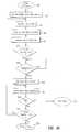
- FIGS. 4 a and 4 billustrate a flow chart of the steps performed by the microprocessor circuit 24 .
- FIG. 5shows an example of the contents of the LUT, maintained in the space manager/flash interface unit 28 of FIG. 1, as it relates to the block information maintained in the memory unit 16 .
- a digital system 10which may be a part of a computer (personal computer (PC)), digital camera and the like is shown in accordance with an embodiment of the present invention to include a host 12 , a controller device 14 and a nonvolatile memory unit 16 .
- the host 12is shown to be coupled to read information from and write information to the memory unit 16 under the direction of the controller device 14 .
- the memory unit 16is comprised of at least two nonvolatile memory devices in accordance with the present invention.
- Each of the nonvolatile memory devicesis an integrated circuit (or semiconductor device, as commonly referred to by the industry).
- the nonvolatile memory devicesmay be flash, EEPROM (Electronically Erasable Programmable Read Only Memory) or other type of solid state memory.
- the host 12is shown to communicate with the controller 14 through host bus 18 and the controller device 14 is shown coupled to the memory unit 16 through memory signals 20 .
- the controller device 14is an integrated circuit (or semiconductor) shown to include a host interface circuit 22 , a microprocessor circuit 24 , a volatile storage unit 26 and a space manager/flash interface circuit 28 .
- the host interface circuit 22is for coupling the host 12 through host bus 18 , which includes an address bus, a bi-directional data bus and control signals (not shown separately).
- the host address and data bussesmay be comprised of a single bus carrying both address and data information by multiplexing address and data signals onto the same bus. It should be noted that the term bus as used herein includes multiple electrical conductors or signal lines.
- the host bus 18may be a PCMCIA interface, an ATA interface or other kinds of interfaces employed by the industry.
- the host interface circuit 22is shown coupled to the host bus 18 and is further shown to be coupled through a microprocessor bus 30 to the microprocessor circuit 24 .
- Microprocessor circuit 24is further coupled to the space manager/flash interface circuit 28 through the microprocessor bus 30 , which facilitates communication of address and data information and control signals therebetween.
- the microprocessor circuit 24is coupled to read and write information to the volatile storage unit 26 through a volatile storage bus 32 .
- the microprocessor circuit 24is an Intel 8051 processor and alternatively, the microprocessor unit 24 may be any general-purpose processor unit.
- the volatile storage unit 26is generally a read-access memory (RAM) for storing firmware code that is executed by the microprocessor circuit 24 .
- Information between the host 12 and the controller 14is transferred through the host bus 18 and information between the controller 14 and the memory unit 16 is coupled through the memory signals 20 .
- the memory unit 16is comprised of two or more nonvolatile memory devices, such as 34 and 36 .
- the size of each of the nonvolatile memory devices 34 and 36may vary depending on the application of the digital system 10 . Nonetheless, this size is generally referred to by bytes where each byte is 8 bits.
- the size of the nonvolatile memory unit 16is 160 MB (mega bytes) together, or 80 MB each.
- the nonvolatile memory devices 34 and 36are of the memory type that preserve their contents even during a power-down.
- Typical examples of nonvolatile memory devicesare flash or EEPROM devices comprised of floating gate cells and manufactured by companies such as Toshiba, Hitachi and the like.
- the space manager/flash interface circuit 28includes a space manager control unit 38 , a flash interface circuit 40 and a space manager storage unit 42 .
- the space manager unit 38in one embodiment of the present invention, is comprised of a state machine for controlling the information that is stored in a look-up-table (LUT) maintained within the space manager storage unit 42 .
- LUTlook-up-table
- the functions of the space manager control unit 38may be performed by other types of hardware and/or software as understood by those of ordinary skill in the art.
- the space manager storage unit 42is of a volatile type of memory, such as RAM, for storing block addressing and status information within the LUT.
- the memory signals 20include a flash address bus, a bi-directional flash data bus and flash control signals. Some of these signals will be further described with respect to other figures included herein.
- the host 12accesses the memory unit 16 from time to time and during performance of various operations such as reading and writing to the memory unit 16 . In doing so, the host 12 provides an address identifying a location for reading or writing of data.
- the host-provided addressis coupled onto the host bus 18 for use by the controller 14 in accessing or reading information to and from the memory unit 16 .
- the host-provided addressis in the form of CHS (cylinder, head and sector). This type of addressing is adopted from systems using hard disks where such an addressing scheme was used to identify a particular location on the disk. With the advent of nonvolatile memory for storage of information however, the CHS address format need be converted to a value for identifying a location within the nonvolatile memory unit.
- the controller 14converts the same to a logical block address (LBA).
- LBAlogical block address
- the LBAis then coupled through the microprocessor bus 30 for use by the space manager/flash interface unit 28 .
- the host 12provides an LBA type of address to the controller 14 , in which case, while conversion is still performed, it is not a CHS to LBA conversion.
- the latter conversionmerely displaces the LBA, as is also performed when the former conversion, i.e. CHS to LBA is used.
- a blockis defined to include a predetermined number of sectors.
- LBA[(Cylinder*Heads+Heads)*Sectors/Track]+(Sector ⁇ 1 (Eq. 1)
- the cluster sizegenerally determines the requisite size of the memory unit 16 since the size of the space manager storage unit 42 is typically fixed. This will become apparent during a later discussion.
- the LBA calculation according to the equation shown abovemay be performed by hardware or firmware. In the case where firmware is used to calculate the LBA, the microprocessor 24 performs such function by execution of the firmware code stored in the volatile storage unit 26 . In the case where hardware is used to calculate the LBA, a state machine block (not shown in FIG. 1) performs such a calculation.
- the LBAis translated to a VLBA (Virtual Logical Block Address) value by masking certain least significant bits of the LBA.
- VLBAVirtual Logical Block Address
- the VLBAis calculated from the LBA by a logical ‘AND’ of the LBA with the hexadecimal value 0 ⁇ 3FFFF0. This essentially results in the LBA being preserved except for the 4 least significant bits thereof.
- the VLBAis calculated by a logic ‘AND’ of the LBA value with the hexadecimal value of 0 ⁇ 3FFFE0, which is effectively masking off the 5 least significant bits of the LBA and preserving the remaining bits, and so on.
- the translation of the LBA to VLBAis performed by the space manager/flash interface 28 . This translation may be performed by either hardware or software.
- the VLBAis then coupled onto the microprocessor bus 30 from the microprocessor 24 to the space manager control unit 38 of the space manager/flash interface circuit 28 where it is used to address the LUT of the space manager storage unit 42 .
- the VLBAis used to address a particular location of the LUT wherefrom a VPBA (virtual physical block address) is retrieved.
- a particular LBA valuemay be used to point to various PBA values. For example, if the host wishes to write to a location that is identified by a particular LBA value, the particular LBA value is then used to look up a VPBA value in the LUT.
- This VPBA valuemay be, for example, ‘20’ but the next time the host wishes to write to the same LBA-identified location, the VPBA value retrieved from the LUT may be ‘200’ rather than ‘20’.
- the way in which this is doneis with the use of certain flag information that is also maintained within the LUT. Briefly, the first time after an erase operation that a particular LBA location is being addressed by the host for writing thereto, the information is written and a flag field within the LUT corresponding the particular LBA is marked as ‘used’ so that the next time the host wishes to write to that same location prior to an erase operation, a different location within the memory unit 16 is identified by a different PBA for such writing.
- a block of informationis typically a sector as employed in conventional hard disk drives, with each sector typically having 512 bytes of data, although other-sized sectors may be similarly employed.
- Microprocessor 24executes instructions in the form of program code from the volatile memory unit 26 (such as ROM (read-only memory) or RAM (read-and-write memory)) located either within or outside of the microprocessor 24 .
- the microprocessor 24further instructs the space manager control unit 38 to use the LBA, originated by a CHS value provided by the host, to find the next unused (or free) addressable storage block location available within the memory unit 16 .
- this unused block locationis stored in the LUT and during a host read operation, this unused block location is read from the LUT.
- the address value identifying the a location within the memory unit 16is referred to as a Virtual Physical Block Address (VPBA).
- VPBAVirtual Physical Block Address
- the space manager control unit 38may employ any one of a variety of algorithms to find the next available (or free) block located within the flash memory devices.
- An example of a space manageris disclosed in an earlier-issued patent, U.S. Pat. No. 5,485,595, entitled “Flash Memory Mass Storage Architecture Incorporating Wear Level Technique Without Using Cam Cells”, issued on Jan. 16, 1996 with the inventors being Mahmud Assar, Petro Estakhri, Siamack Nemazie and Mahmood Mozaffari, the disclosure of which is herein incorporated by reference as though set forth in full. The reader is particularly directed to FIGS. 11-13 and discussions regarding the same. In alternative embodiments, however, other space management methods and apparatus may likewise be employed by the present invention.
- the VLBA valueis ultimately used to look up a VPBA value from the LUT.
- the LUTis comprised of rows and columns with each row being addressed by a VLBA value.
- the VLBA valueis used to address a particular row of the LUT for retrieving therefrom, the VPBA, which includes certain flag information.
- the VLBAis used to address a particular row of the LUT for storing a VPBA value including certain flag information.
- the VPBAis ultimately translated to a Physical Block Address (PBA) for identifying a particular sector location within the memory unit 16 .
- PBAPhysical Block Address
- mapping of address informationis perhaps best understood with the use of an example.
- a ‘super’ blockis a block comprising of a plurality of blocks with each block residing in a location within a flash device that is the same relative location as that of the remaining blocks in the remaining flash device.
- blocks of a super blockare positioned in like-locations within each of the flash devices and each block of a super block is within one flash device thereby positioning the blocks of a super block in-parallel with respect to each other.
- An LBA, derived, if need be, from a CHS value sent by the host 12is calculated in accordance with the equation above.
- the LBA valueis then coupled onto the microprocessor bus 30 by the microprocessor 24 for use by the space manager/flash interface 28 where it is translated to a VLBA address.
- the LBA value shown in Table 1includes 4 bits of sector information, 10 bits of block information and 5 bits of chip select information. Four bits of sector indicates the use of 16 sectors per block since 2 to the power of 4 equals 16.
- the VLBAis derived by masking the sector bits (the masked sector bits will be referred to as sector offset value), which in this example include 4 bits.
- the block and chip select informationremain the same.
- the chip select bitsare used to select a particular one of the plurality of nonvolatile memory devices included within the memory unit 16 , such as one of the devices 34 or 36 .
- the block informationidentifies a particular block within the selected nonvolatile memory device.
- the VPBA valueis shown to include 4 least significant bits (LSBs) as ‘don't care’ bits, which indicates that those bits carry no meaningful information, followed by eight block information bits and five chip select bits and three flag bits.
- the three flag bitsare shown as ‘UOD’, respectively.
- ‘U’indicates a ‘used’ flag
- ‘O’stands for ‘old’ flag
- ‘D’stands for ‘defect’ flag.
- ‘C’sindicate bits that carry chip select information while ‘B’s indicate bits that carry block information and ‘S’s carry sector information.
- the chip select informationis used for addressing a particular nonvolatile memory device within the memory unit 16 while block information is used for identifying a particular block within the selected nonvolatile memory device and sector information is used for identifying a sector, although the latter is not used by the LUT, as the sector bits are masked.
- the VPBAis converted to a PBA value by shifting the VPBA value to the left so as to eliminate flag information and by appending the sector offset value. There are a number of ‘0’s appended, as LSBs, to the PBA in order to account for expansion of the size of the memory unit 16 .
- the size of the LUT or the size of the space manager storage unit 42 (in FIG. 1)is generally fixed.
- the LUThas 5120 rows or entries with each row or entry being 24 bits wide. Accordingly, since the LUT size remains the same, the size of the cluster, or the number of sectors per block, dictates the size of the memory unit 16 being employed.
- the size of the memory unit 16is often referred to as the memory capacity.
- the size of each blockis a determination of the size of the requisite nonvolatile memory capacity.
- the cluster sizein Table 2, as discussed earlier, represents the number of sectors in a block. For example, in prior art systems, where a 40 MB nonvolatile memory capacity is being employed, each block includes 16 sectors. Whereas, for a 80 MB capacity, 32 sectors per block (or cluster size) is employed. This is again, in part, due to the number of LUT entries remaining the same, i.e. 5120.
- blocksare numbered sequentially in the nonvolatile memory unit 16 and blocks are erased sequentially by selecting a particular nonvolatile memory devices among the devices within the memory unit 16 , issuing an erase command followed by the address of the block to be erased and subsequently verifying whether or not the erase operation was successful by reading the contents of the erased block and comparing it to an all ‘1’s value.
- successful erasure of flash or nonvolatile memory cellsentails programming the cells to a logic state of ‘1’. Once erased, a cell can be written to but only once before it must be erased in order to be capable of being re-written.
- a ‘super’ blockis defined by a number of blocks that are in like locations of the different nonvolatile memory devices and residing in-parallel with respect to each other. According to the information provided in the following Table 3, below,
- the SPM Entry or LUT rowsremain the same, i.e. 5120 but the intent is to have a 320 Mbyte nonvolatile memory capacity size, i.e. this is the total size of the memory unit 16 .
- the memory unit 16is then managed as 128 sectors/cluster. For example, according to the above, if a block is defined to include 16 sectors, a ‘super’ block will include 8*16 or 128 sectors with each 16-sector block being stored in one nonvolatile memory device and eight such nonvolatile memory devices being used in-parallel to define 8 blocks. This is perhaps best understood using an example to show the management of the memory unit 16 when using 32 sectors/block and a ‘super’ block having 4 blocks, as shown in FIG. 2 .
- the number of sectorsdefines an erasable block.
- an erasable blockconsists of 16 sectors and in the second row of that column, an erasable block is shown to consist of 32 sectors and so on.
- the Nonvolatile Memory Capacity columnreflects the total capacity of the memory unit 16 and the flash devices are the nonvolatile memory devices within the memory unit 16 .
- a total memory size of 160 MBis made up of twenty 8 MB-flash devices.
- a flash memory unit 200is shown to include 4 flash memory devices, 202 - 208 .
- a super blockthen includes 4 blocks.
- a super blockis denoted in FIG. 2 by the reference number 210 and as shown spreads over 4 flash memory devices. Blocks are numbered horizontally through the flash memory devices 202 - 208 such that, for example, the blocks included within the first super block, i.e. blocks 0 - 3 , are each stored within the first block row of each of the flash memory devices 202 - 208 , respectively.
- blocks 4 - 7which belong to the second super block, are stored within the second block row of the flash devices 202 - 208 , respectively.
- Each of the flash devices 202 - 208is shown to include 1024 block rows.
- Each block rowis a storage space of 32 sectors*512 bytes or 16 KB since each sector is 512 bytes.
- An entire super blockis erased as a unit during an erase operation. For example, if the first super block is to be erased, the flash device 202 is first selected and an erase operation command is issued along with an address identifying the first block of the flash device 202 . Next, the second flash device, or flash device 204 , is selected, followed by another erase operation command and an address identifying the first block of the flash device 204 (this value will be the same as the value used in identifying the first block of the flash device 202 ). Next, flash device 206 is selected and a read operation command is issued in the same manner as is done with respect to the flash device 208 .
- a ‘read status’ commandis performed by issuing a read status command to check for the erase operation being completed without errors, i.e., checking for the contents of the erased blocks of each of the flash devices 202 - 208 being at logic state ‘1’ and if so, the erased blocks are used for further writing thereto.
- the signals used for coupling information between the controller 14 and the memory unit 16include various address, data and control signals for effectuating not only erase but also read and write operations (the latter two operations having been initiated by the host 12 ). Some of these signals included within the memory signals 18 will be referred to in the following discussion with respect to FIG. 3 and shown therein.
- the sequence of activities during an erase operationis shown in a timing diagram in FIG. 3, as an example, where two flash devices are employed. This may be the case where a block includes 64 sectors to form 160 MB nonvolatile memory capacity shown in Table 3 above.
- the signals, CLE 0 302 , CLE 1 304 , CLE 2 301 and CLE 3 303 , /WE 306 , address 308 , Read/Busy* 310are shown as being included in the memory signals 18 (in FIG. 1 ).
- This exampleassumes there are four flash devices in the memory unit 16 (in FIG. 1 ).
- the signals 302 , 304 , 301 and 303are chip enable or chip select signals that select one of the four flash devices when active (active in this example refers to a logical state of ‘1’).
- the /WE 306 signalis a write enable signal that is activated whenever address or data is being written to one of the flash devices. Activated of the 306 signal is a logic state of ‘0’.
- the address signals 308provide the command and address portions of an operation. The address being the address of a block within a flash device and the command being one of read, write or erase operations. In the sequence of events, a command is first provided by the controller 12 through the address signals 308 to the memory unit 16 , followed by the address of the block, in byte form, with the high byte being transmitted first followed by the low byte.
- the Ready/Busy* signal, 310indicates whether a corresponding flash device is ready or busy. At logic state ‘1’, the Ready/Busy* signal indicates that the corresponding flash device is ready for being written thereto, read from or erased, whereas, a logic state of ‘0’ indicates that the corresponding flash device is busy and operation thereupon is not allowed.
- a super blockis comprised of four blocks so that an erase operation includes erasing four blocks that are located in the same position within the four flash devices.
- the CLE 0 signal 302When an erase operation takes place in accordance with the present invention, the CLE 0 signal 302 is activated and an erase command is coupled onto the address signals 308 (this is indicated by the value ‘60’ in hexadecimal notation in FIG. 3 ). When so doing, the /WE signal 306 is asserted or activated. Furthermore, with the assertion of the CLE 0 signal 302 , the first flash device is enabled. Next, the CLE 1 signal 304 is activated in order to enable the second flash device and the address of the block being erased is coupled onto the address signals 308 , followed by causing the signal 310 to go to a logic state of ‘ 0 ’ to indicate that the first flash device is now busy.
- a super blockis being erased during an erase operation with a super block including a plurality blocks, as determined by the sector size of a block. It has been the inventors' experience that the time frame, indicated by reference number 314 in FIG. 3, when the flash devices are busy being erased, is 2.3 milliseconds in accordance with the present invention when four flash devices are employed, whereas the same time frame is 8 milliseconds for prior art erase operations. This results in an overall system performance improvement of approximately 20%.
- the inventors' experiencehas been that the time for performing an erase operation, measured as indicated by 314 but for two devices, is reduced from 4 to 2.3 milliseconds in accordance with the present invention.
- the more flash devices being employedthe more time is saved for performing an erase operation with the use of the structure and methods of the present invention.
- the chip select signals and other addressing informationare derived from the PBA.
- ‘C’sindicate chip select and if only two flash devices are being employed, CLE 0 and CLE 1 signals are developed from the value of the ‘C’s.
- a two-bit (or ‘C’s)would be required and if these two bits are at logic state ‘0’, then the CLE 0 signal is activated and if they are at logic state ‘1’, then the CLE 1 signal is activated and if they are at logic state ‘2’, the CLE 2 signal is activated and if they are at logic state ‘3’, the CLE 3 signal is activated.
- the ‘B’s and ‘S’sform the address signals 308 .
- FIGS. 4 a and 4 billustrate a flow chart showing the steps performed by the controller 14 (shown in FIG. 1) when writing one sector of information to the memory unit 16 (shown in FIG. 1 ). These steps may be performed by hardware or software (firmware). In one embodiment of the present invention, these steps are performed by the microprocessor circuit 24 by executing the firmware code stored in the volatile storage unit 26 .
- the host 12sends and the controller 14 receives a CHS address where the host is interested in writing data within the memory unit 16 .
- the controller 14checks the received CHS address at 402 to determine whether or not the address is valid. Upon power-on, the host will issue an identification command—This command will return memory card parameters (maximum cylinder, head, sector and track information including maximum LBA value). If the received CHS address is not a valid address, the controller 14 returns an error message back to the host. If on the other hand, the received address is valid, the process continues to step 406 .
- the controller 14calculates a LBA from the CHS address that was sent by the host. This calculation is done in accordance with equation 1 as recited hereinabove.
- a particular location of bufferis preserved for storing the data that is to be later programmed into the memory unit 16 . This particular buffer area is not shown in FIG. 1 although it is composed of RAM.
- the LBAis translated to VLBA. This is done by logically ‘ANDing’ the LBA with a hexadecimal value ‘0 ⁇ 3FFFF0H.’ Essentially by doing so all of the bits in the LBA are preserved except for the four least significant bits. This is for the case where 16 sectors per block are employed.
- the VLBAis calculated by logically ‘ANDing’ the LBA by the hexadecimal value 0 ⁇ 3FFFE0H. This preserves the LBA except for the five least significant bits, and in the case where there are 64 sectors per block, the VLBA is calculated by logically ‘ANDing’ the LBA by the hexadecimal value 0 ⁇ 3FFFC0H where all of the LBA bits are preserved except for the six least significant bits thereof. In cases where other sector sizes are being employed the calculation of VLBA is performed in a similar fashion.
- the data that is to be written to the memory unit 16is written by the host to a buffer located within the controller.
- the VLBAis checked to determine whether the address that the host is currently interested in writing to has been previously written. If so, that is, if the address is one that has been previously written, then at step 416 the VPBA is obtained from the LUT using the VLBA as explained hereinabove. The process then continues to step 420 where the block that was checked at 414 is marked as ‘old’ and the process then continues to step 418 .
- the sector informationis that portion of the LBA that was earlier masked. In other words, the four least significant bits that were masked at step 410 are now appended to the VPBA to obtain PBA.
- a searchis performed by the space manager to obtain a free block for writing thereto.
- the ‘used’ flagis set to indicate that the block is now in use and contains data and then a write operation is performed to write the data into the appropriate VPBA.
- the PBAis converted to a FAP (flash address pointer) value.
- the FAPserves as a value that identifies the particular chip, the non-volatile device, within the memory unit 16 being written to and the particular sector therein that is being written thereto. For example, the FAP value is broken down such that the four most significant bits of the PBA value indicate the chip select. The next nine bits indicate the sector select value and the least four significant bits of the PBA indicate the offset. In this example, the FAP has a 17 bit value.
- step 426data is written to the appropriate sector, as defined by the FAP, of one of the non-volatile memory devices of the memory unit 16 , and at step 428 a check is performed for errors That is, the hardware or firmware will issue a command to read the flash status and if the flash reports that the write operation completed successfully, there is no error reported, otherwise, failure to successfully program the flash device is reported as an error.
- the processcontinues to 430 where the block is considered defective and designated as no longer being used and another block is searched for writing thereto. If, on the other hand, the error check at step 428 is determined to yield a result where no errors are detected the process continues to step 432 where the remainder of the cluster or block is moved to the block where the host data was written, and at step 434 the old cluster or block is erased.
- step 438where the parallel erase chip counter is set.
- the PBA valueis converted to FAP and at step 442 an erase flash command is issued by the controller 14 .
- step 444the PBA value is increased to indicate the next non-volatile memory device within the memory unit 16 and the erase counter which was set at step 438 is decremented by one at step 446 and checked as to whether it is equal to zero after it has been decremented. If at step 446 it is determined that the erase counter is not equal to zero the process goes back to step 440 and continues on through steps 440 through 446 until the erase counter is equal to zero.
- the processcontinues to 448 .
- the Ready/Busy* signal 310is checked. If the signal indicates that the memory unit 16 is busy, in other words, if the Ready/Busy* signal 310 is zero, the process continues back to step 448 and loops onto itself until the signal 310 indicates ready, and then continues to step 450 .
- step 450the erase counter is set. Thereafter, at step 452 the read status command is issued and the process continues to 454 where error is checked therefor. If no errors are reported the process continues to step 458 . If an error exists the test continues to 456 where an error message is returned.
- step 458the erase counter that was set at step 450 is decremented and checked against zero. If the erase counter is equal to zero the process continues to 460 where essentially the erase operation is completed, and if the erase counter is not equal to zero after it has been decremented, the process continues to step 452 where steps 452 through 458 are repeated until the erase counter is set equal to zero. This completes the steps performed during a write operation of the sector in accordance with an embodiment of the present invention.
- FIG. 5shows an example of the contents of the LUT as it relates to the memory unit 16 .
- a 160 MB memory unitis employed and on the left hand side of FIG. 5 there is shown a column that is the VLBA whose values are used to look up information in the LUT.
- the VPBA informationthere is maintained the VPBA information.
- Each of the VLBAscorresponds to a VPBA.
- Each of the VPBA valuescorresponds to four blocks that make up a super block within the flash devices of the memory unit 16 which is shown on the right hand side of FIG. 5 under the PBA column.
- a VLBA value of zerocorresponds to a VPBA value of zero which then corresponds to four blocks that are BLKO.
- Each blockwill be within one flash or non-volatile memory device. This is indicated by the arrows extending from VPBA value zero which is the first entry in the LUT to each of the flash devices 0 - 3 .
- a VLBA value of 200 in hexadecimal notationcorresponds to VPBA value of 20 in hexadecimal notation which is then used to point to block one of each of the flash devices zero through three, or each of the four flash devices.
- Each flash devicehas blocks therein.
- the FAP valueis calculated from the PBA value and appended to the LBA offset value.
Landscapes
- Engineering & Computer Science (AREA)
- Theoretical Computer Science (AREA)
- Microelectronics & Electronic Packaging (AREA)
- Physics & Mathematics (AREA)
- General Engineering & Computer Science (AREA)
- General Physics & Mathematics (AREA)
- Techniques For Improving Reliability Of Storages (AREA)
- Memory System (AREA)
- Read Only Memory (AREA)
- Non-Volatile Memory (AREA)
Abstract
Description
| TABLE 1 | |||
| LBA | |||
| xxxx,xCCC,BBBB,BBBB,BBCC,SSSS | |||
| PBA | |||
| Xxxx,xCCC,CCBB,BBBB,BBxx,xxxx | |||
| VPBA | |||
| Xxxx,UODC,CCCC,BBBB,BBBB,xxxx | |||
| For | ||
| C:Chip, B:Block, S:Sector, U:Used, O:Old, D:Defect | ||
| TABLE 2 | ||||
| Cluster Size | SPM Entry | |||
| 16 sectors | 5120 | 40MB (5120 * 8KB) | ||
| 32 sectors | 5120 | 80MB (5120 * 16KB) | ||
| 64 sectors | 5120 | 160MB (5120 * 32KB) | ||
| TABLE 3 | ||
| Cluster Size | SPM Entry | |
| 4 * 16 sectors | 5120 | 160MB (64-Mbit flash devices) |
| 4 * 32 sectors | 5120 | 320MB (128/256-Mbit flash devices) |
Claims (18)
Priority Applications (1)
| Application Number | Priority Date | Filing Date | Title |
|---|---|---|---|
| US09/610,545US6262918B1 (en) | 1999-04-01 | 2000-06-30 | Space management for managing high capacity nonvolatile memory |
Applications Claiming Priority (3)
| Application Number | Priority Date | Filing Date | Title |
|---|---|---|---|
| US09/283,728US6034897A (en) | 1999-04-01 | 1999-04-01 | Space management for managing high capacity nonvolatile memory |
| US09/519,226US6134151A (en) | 1999-04-01 | 2000-03-06 | Space management for managing high capacity nonvolatile memory |
| US09/610,545US6262918B1 (en) | 1999-04-01 | 2000-06-30 | Space management for managing high capacity nonvolatile memory |
Related Parent Applications (1)
| Application Number | Title | Priority Date | Filing Date |
|---|---|---|---|
| US09/519,226ContinuationUS6134151A (en) | 1999-04-01 | 2000-03-06 | Space management for managing high capacity nonvolatile memory |
Publications (1)
| Publication Number | Publication Date |
|---|---|
| US6262918B1true US6262918B1 (en) | 2001-07-17 |
Family
ID=26962208
Family Applications (1)
| Application Number | Title | Priority Date | Filing Date |
|---|---|---|---|
| US09/610,545Expired - LifetimeUS6262918B1 (en) | 1999-04-01 | 2000-06-30 | Space management for managing high capacity nonvolatile memory |
Country Status (6)
| Country | Link |
|---|---|
| US (1) | US6262918B1 (en) |
| EP (2) | EP1228510B1 (en) |
| AT (1) | ATE340405T1 (en) |
| AU (1) | AU4061700A (en) |
| DE (1) | DE60030876T2 (en) |
| WO (1) | WO2000060605A1 (en) |
Cited By (56)
| Publication number | Priority date | Publication date | Assignee | Title |
|---|---|---|---|---|
| US20020112101A1 (en)* | 1998-03-02 | 2002-08-15 | Petro Estakhri | Flash memory card with enhanced operating mode detection and user-friendly interfacing system |
| US6442067B1 (en)* | 2000-05-23 | 2002-08-27 | Compaq Information Technologies Group, L.P. | Recovery ROM for array controllers |
| US20030135688A1 (en)* | 2002-01-11 | 2003-07-17 | Shih-Chieh Tai | Flash memory data access method and configuration |
| US20030161199A1 (en)* | 2002-02-22 | 2003-08-28 | Petro Estakhri | Removable memory media with integral indicator light |
| WO2004001604A1 (en)* | 2002-06-19 | 2003-12-31 | Hyperstone Ag | Method for addressing memories that can be deleted in blocks |
| US6772274B1 (en) | 2000-09-13 | 2004-08-03 | Lexar Media, Inc. | Flash memory system and method implementing LBA to PBA correlation within flash memory array |
| US6772273B1 (en) | 2000-06-29 | 2004-08-03 | Intel Corporation | Block-level read while write method and apparatus |
| US20040259320A1 (en)* | 2002-08-15 | 2004-12-23 | Holscher Richard D. | Use of a dual-tone resist to form photomasks including alignment mark protection, intermediate semiconductor device structures and bulk semiconductor device substrates |
| US6901457B1 (en) | 1998-11-04 | 2005-05-31 | Sandisk Corporation | Multiple mode communications system |
| US20050138247A1 (en)* | 2003-12-22 | 2005-06-23 | Kabushiki Kaisha Toshiba | Emulation system and emulation method |
| US20050172065A1 (en)* | 2004-01-30 | 2005-08-04 | Micron Technology, Inc. | Data move method and apparatus |
| US6950918B1 (en) | 2002-01-18 | 2005-09-27 | Lexar Media, Inc. | File management of one-time-programmable nonvolatile memory devices |
| US20050213399A1 (en)* | 2004-03-29 | 2005-09-29 | Hoover Patricia J | Method and apparatus to write data |
| US6957295B1 (en) | 2002-01-18 | 2005-10-18 | Lexar Media, Inc. | File management of one-time-programmable nonvolatile memory devices |
| US6973519B1 (en) | 2003-06-03 | 2005-12-06 | Lexar Media, Inc. | Card identification compatibility |
| US6978342B1 (en) | 1995-07-31 | 2005-12-20 | Lexar Media, Inc. | Moving sectors within a block of information in a flash memory mass storage architecture |
| US20060031627A1 (en)* | 2001-01-19 | 2006-02-09 | Conley Kevin M | Partial block data programming and reading operations in a non-volatile memory |
| US7000064B2 (en) | 2001-09-28 | 2006-02-14 | Lexar Media, Inc. | Data handling system |
| US20060039196A1 (en)* | 2003-10-03 | 2006-02-23 | Gorobets Sergey A | Corrected data storage and handling methods |
| US20060069896A1 (en)* | 2004-09-27 | 2006-03-30 | Sigmatel, Inc. | System and method for storing data |
| US20060106949A1 (en)* | 2004-11-12 | 2006-05-18 | Emulex Design & Manufacturing Corporation | Legacy-compatible extended command input-output control block |
| US20060123160A1 (en)* | 2004-12-03 | 2006-06-08 | Emulex Design & Manufacturing Corporation | Interrupt notification block |
| US20060136655A1 (en)* | 2004-12-16 | 2006-06-22 | Gorobets Sergey A | Cluster auto-alignment |
| US20060161722A1 (en)* | 2004-12-16 | 2006-07-20 | Bennett Alan D | Scratch pad block |
| US7102671B1 (en) | 2000-02-08 | 2006-09-05 | Lexar Media, Inc. | Enhanced compact flash memory card |
| US7111140B2 (en) | 1995-07-31 | 2006-09-19 | Lexar Media, Inc. | Increasing the memory performance of flash memory devices by writing sectors simultaneously to multiple flash memory devices |
| US20060256624A1 (en)* | 2003-06-24 | 2006-11-16 | Micron Technology, Inc. | Erase block data splitting |
| US7139199B2 (en)* | 2004-06-28 | 2006-11-21 | Intel Corporation | Flash memory file system with transacted operations |
| US7155559B1 (en) | 2000-08-25 | 2006-12-26 | Lexar Media, Inc. | Flash memory architecture with separate storage of overhead and user data |
| US7167944B1 (en) | 2000-07-21 | 2007-01-23 | Lexar Media, Inc. | Block management for mass storage |
| US7185208B2 (en) | 2001-09-28 | 2007-02-27 | Lexar Media, Inc. | Data processing |
| US7215580B2 (en) | 2001-09-28 | 2007-05-08 | Lexar Media, Inc. | Non-volatile memory control |
| US7231643B1 (en) | 2002-02-22 | 2007-06-12 | Lexar Media, Inc. | Image rescue system including direct communication between an application program and a device driver |
| US7254724B2 (en) | 2001-09-28 | 2007-08-07 | Lexar Media, Inc. | Power management system |
| US7275686B2 (en) | 2003-12-17 | 2007-10-02 | Lexar Media, Inc. | Electronic equipment point-of-sale activation to avoid theft |
| US7340581B2 (en) | 2001-09-28 | 2008-03-04 | Lexar Media, Inc. | Method of writing data to non-volatile memory |
| US20080067642A1 (en)* | 2002-08-08 | 2008-03-20 | Micron Technology, Inc. | Packaged microelectronic components |
| US7370166B1 (en) | 2004-04-30 | 2008-05-06 | Lexar Media, Inc. | Secure portable storage device |
| US20080140724A1 (en)* | 2006-12-06 | 2008-06-12 | David Flynn | Apparatus, system, and method for servicing object requests within a storage controller |
| US20080205153A1 (en)* | 2007-02-23 | 2008-08-28 | Samsung Electronics Co., Ltd. | Method and apparatus for controlling two or more non-volatile memory devices |
| US7464306B1 (en) | 2004-08-27 | 2008-12-09 | Lexar Media, Inc. | Status of overall health of nonvolatile memory |
| US7484070B1 (en) | 2004-01-09 | 2009-01-27 | Conexant Systems, Inc. | Selective memory block remapping |
| US7523249B1 (en) | 1995-07-31 | 2009-04-21 | Lexar Media, Inc. | Direct logical block addressing flash memory mass storage architecture |
| US20090150605A1 (en)* | 2007-12-06 | 2009-06-11 | David Flynn | Apparatus, system, and method for converting a storage request into an append data storage command |
| US7594063B1 (en) | 2004-08-27 | 2009-09-22 | Lexar Media, Inc. | Storage capacity status |
| US20100031000A1 (en)* | 2007-12-06 | 2010-02-04 | David Flynn | Apparatus, system, and method for validating that a correct data segment is read from a data storage device |
| US20100077135A1 (en)* | 2008-09-23 | 2010-03-25 | Via Telecom, Inc. | Memory wear leveling method, system and device |
| US7725628B1 (en) | 2004-04-20 | 2010-05-25 | Lexar Media, Inc. | Direct secondary device interface by a host |
| US20100228928A1 (en)* | 2009-03-04 | 2010-09-09 | Micron Technology, Inc. | Memory block selection |
| US20100228940A1 (en)* | 2009-03-04 | 2010-09-09 | Micron Technology, Inc. | Memory block management |
| US7917709B2 (en) | 2001-09-28 | 2011-03-29 | Lexar Media, Inc. | Memory system for data storage and retrieval |
| US20110219177A1 (en)* | 2008-04-24 | 2011-09-08 | Shinichi Kanno | Memory system and control method thereof |
| US8122322B2 (en) | 2007-07-31 | 2012-02-21 | Seagate Technology Llc | System and method of storing reliability data |
| US8171203B2 (en) | 1995-07-31 | 2012-05-01 | Micron Technology, Inc. | Faster write operations to nonvolatile memory using FSInfo sector manipulation |
| US8209474B1 (en)* | 2009-09-30 | 2012-06-26 | Emc Corporation | System and method for superblock data writes |
| US8588017B2 (en) | 2010-10-20 | 2013-11-19 | Samsung Electronics Co., Ltd. | Memory circuits, systems, and modules for performing DRAM refresh operations and methods of operating the same |
Families Citing this family (2)
| Publication number | Priority date | Publication date | Assignee | Title |
|---|---|---|---|---|
| US7412560B2 (en)* | 2004-12-16 | 2008-08-12 | Sandisk Corporation | Non-volatile memory and method with multi-stream updating |
| FR2980905B1 (en)* | 2011-09-29 | 2014-03-14 | Continental Automotive France | METHOD FOR ERASING MEMORIZED INFORMATION IN NON-VOLATILE REINSTRIPTIBLE MEMORY, MEMORY STORAGE MEDIUM AND AUTOMOTIVE VEHICLE CALCULATOR |
Citations (71)
| Publication number | Priority date | Publication date | Assignee | Title |
|---|---|---|---|---|
| US4210959A (en) | 1978-05-10 | 1980-07-01 | Apple Computer, Inc. | Controller for magnetic disc, recorder, or the like |
| US4355376A (en) | 1980-09-30 | 1982-10-19 | Burroughs Corporation | Apparatus and method for utilizing partially defective memory devices |
| US4405952A (en) | 1978-05-26 | 1983-09-20 | Cii Honeywell Bull | Apparatus for detecting faulty sectors and for allocating replacement sectors in a magnetic disc memory |
| JPS58215795A (en) | 1982-06-08 | 1983-12-15 | Toshiba Corp | Non-volatile memory device |
| JPS58215794A (en) | 1982-06-08 | 1983-12-15 | Toshiba Corp | Non-volatile memory device |
| WO1984000628A1 (en) | 1982-07-30 | 1984-02-16 | Western Electric Co | Management of defects in storage media |
| JPS5945695A (en) | 1982-09-07 | 1984-03-14 | Fujitsu Ltd | Ic memory |
| US4450559A (en) | 1981-12-24 | 1984-05-22 | International Business Machines Corporation | Memory system with selective assignment of spare locations |
| US4456971A (en) | 1981-02-09 | 1984-06-26 | Sony Corporation | Semiconductor RAM that is accessible in magnetic disc storage format |
| JPS59162695A (en) | 1983-03-07 | 1984-09-13 | Nec Corp | Storage device |
| US4525839A (en) | 1981-10-30 | 1985-06-25 | Hitachi, Ltd. | Method of controlling storage device |
| JPS60212900A (en) | 1984-04-09 | 1985-10-25 | Nec Corp | Semiconductor fixed memory |
| JPS6196598A (en) | 1984-10-17 | 1986-05-15 | Fuji Electric Co Ltd | Electrically erasable P-ROM count data storage method |
| US4616311A (en) | 1980-10-03 | 1986-10-07 | Tokyo Shibaura Denki Kabushiki Kaisha | Data processing system |
| AU557723B2 (en) | 1982-12-17 | 1987-01-08 | Blue Circle Southern Cement Ltd. | Electronic memory system |
| US4654847A (en) | 1984-12-28 | 1987-03-31 | International Business Machines | Apparatus for automatically correcting erroneous data and for storing the corrected data in a common pool alternate memory array |
| EP0220718A2 (en) | 1985-10-29 | 1987-05-06 | Toppan Printing Co., Ltd. | IC card |
| JPS62173496A (en) | 1986-01-28 | 1987-07-30 | 日本電気株式会社 | Reference pattern registering circuit |
| EP0243503A1 (en) | 1985-10-28 | 1987-11-04 | Matsushita Electric Industrial Co., Ltd. | Data recording/regenerating device |
| US4710871A (en) | 1982-11-01 | 1987-12-01 | Ncr Corporation | Data transmitting and receiving apparatus |
| JPS62283497A (en) | 1986-05-31 | 1987-12-09 | Canon Inc | Memory write control method |
| US4746998A (en) | 1985-11-20 | 1988-05-24 | Seagate Technology, Inc. | Method for mapping around defective sectors in a disc drive |
| US4757474A (en) | 1986-01-28 | 1988-07-12 | Fujitsu Limited | Semiconductor memory device having redundancy circuit portion |
| JPS63183700A (en) | 1987-01-26 | 1988-07-29 | Mitsubishi Electric Corp | EEPROM access method |
| US4774700A (en) | 1985-03-12 | 1988-09-27 | Matsushita Electric Industrial Co., Ltd. | Information recording and reproducing apparatus with detection and management of defective sectors |
| US4800520A (en) | 1985-10-29 | 1989-01-24 | Kabushiki Kaisha Toshiba | Portable electronic device with garbage collection function |
| US4896262A (en) | 1984-02-24 | 1990-01-23 | Kabushiki Kaisha Meidensha | Emulation device for converting magnetic disc memory mode signal from computer into semiconductor memory access mode signal for semiconductor memory |
| US4914529A (en) | 1988-07-18 | 1990-04-03 | Western Digital Corp. | Data disk defect handling using relocation ID fields |
| US4920518A (en) | 1985-04-23 | 1990-04-24 | Hitachi, Ltd. | Semiconductor integrated circuit with nonvolatile memory |
| US4924331A (en) | 1985-11-20 | 1990-05-08 | Seagate Technology, Inc. | Method for mapping around defective sectors in a disc drive |
| US4953122A (en) | 1986-10-31 | 1990-08-28 | Laserdrive Ltd. | Pseudo-erasable and rewritable write-once optical disk memory system |
| EP0424191A2 (en) | 1989-10-17 | 1991-04-24 | Sundisk Corporation | Device and method for defect handling in semi-conductor memory |
| US5070474A (en) | 1988-07-26 | 1991-12-03 | Disk Emulation Systems, Inc. | Disk emulation system |
| EP0489204A1 (en) | 1990-12-04 | 1992-06-10 | Hewlett-Packard Limited | Reprogrammable data storage device |
| JPH04332999A (en) | 1991-05-07 | 1992-11-19 | Hitachi Koki Co Ltd | Method of using memory |
| US5168465A (en) | 1988-06-08 | 1992-12-01 | Eliyahou Harari | Highly compact EPROM and flash EEPROM devices |
| EP0522780A2 (en) | 1991-07-12 | 1993-01-13 | International Business Machines Corporation | Control method for a computer memory device |
| US5198380A (en) | 1988-06-08 | 1993-03-30 | Sundisk Corporation | Method of highly compact EPROM and flash EEPROM devices |
| EP0544252A2 (en) | 1991-11-28 | 1993-06-02 | Fujitsu Limited | Data management system for programming-limited type semiconductor memory and IC memory card having the data management system |
| US5226168A (en) | 1989-04-25 | 1993-07-06 | Seiko Epson Corporation | Semiconductor memory configured to emulate floppy and hard disk magnetic storage based upon a determined storage capacity of the semiconductor memory |
| FR2687811A1 (en) | 1992-02-20 | 1993-08-27 | Fujitsu Ltd | FLASH MEMORY CONTROL METHOD AND APPARATUS. |
| US5268870A (en) | 1988-06-08 | 1993-12-07 | Eliyahou Harari | Flash EEPROM system and intelligent programming and erasing methods therefor |
| US5268318A (en) | 1988-06-08 | 1993-12-07 | Eliyahou Harari | Highly compact EPROM and flash EEPROM devices |
| US5270979A (en) | 1991-03-15 | 1993-12-14 | Sundisk Corporation | Method for optimum erasing of EEPROM |
| US5293560A (en) | 1988-06-08 | 1994-03-08 | Eliyahou Harari | Multi-state flash EEPROM system using incremental programing and erasing methods |
| US5297148A (en) | 1989-04-13 | 1994-03-22 | Sundisk Corporation | Flash eeprom system |
| US5303198A (en) | 1990-09-28 | 1994-04-12 | Fuji Photo Film Co., Ltd. | Method of recording data in memory card having EEPROM and memory card system using the same |
| US5315541A (en) | 1992-07-24 | 1994-05-24 | Sundisk Corporation | Segmented column memory array |
| US5337275A (en) | 1992-10-30 | 1994-08-09 | Intel Corporation | Method for releasing space in flash EEPROM memory array to allow the storage of compressed data |
| US5341339A (en) | 1992-10-30 | 1994-08-23 | Intel Corporation | Method for wear leveling in a flash EEPROM memory |
| US5341330A (en) | 1992-10-30 | 1994-08-23 | Intel Corporation | Method for writing to a flash memory array during erase suspend intervals |
| US5353256A (en) | 1993-06-30 | 1994-10-04 | Intel Corporation | Block specific status information in a memory device |
| US5357475A (en) | 1992-10-30 | 1994-10-18 | Intel Corporation | Method for detaching sectors in a flash EEPROM memory array |
| US5388083A (en) | 1993-03-26 | 1995-02-07 | Cirrus Logic, Inc. | Flash memory mass storage architecture |
| US5396468A (en) | 1991-03-15 | 1995-03-07 | Sundisk Corporation | Streamlined write operation for EEPROM system |
| US5422842A (en) | 1993-07-08 | 1995-06-06 | Sundisk Corporation | Method and circuit for simultaneously programming and verifying the programming of selected EEPROM cells |
| US5428621A (en) | 1992-09-21 | 1995-06-27 | Sundisk Corporation | Latent defect handling in EEPROM devices |
| US5430859A (en) | 1991-07-26 | 1995-07-04 | Sundisk Corporation | Solid state memory system including plural memory chips and a serialized bus |
| US5438573A (en) | 1991-09-13 | 1995-08-01 | Sundisk Corporation | Flash EEPROM array data and header file structure |
| US5479638A (en) | 1993-03-26 | 1995-12-26 | Cirrus Logic, Inc. | Flash memory mass storage architecture incorporation wear leveling technique |
| US5485595A (en) | 1993-03-26 | 1996-01-16 | Cirrus Logic, Inc. | Flash memory mass storage architecture incorporating wear leveling technique without using cam cells |
| US5504760A (en) | 1991-03-15 | 1996-04-02 | Sandisk Corporation | Mixed data encoding EEPROM system |
| US5508971A (en) | 1994-10-17 | 1996-04-16 | Sandisk Corporation | Programmable power generation circuit for flash EEPROM memory systems |
| US5532962A (en) | 1992-05-20 | 1996-07-02 | Sandisk Corporation | Soft errors handling in EEPROM devices |
| US5535328A (en) | 1989-04-13 | 1996-07-09 | Sandisk Corporation | Non-volatile memory system card with flash erasable sectors of EEprom cells including a mechanism for substituting defective cells |
| US5534456A (en) | 1994-05-25 | 1996-07-09 | Sandisk Corporation | Method of making dense flash EEPROM cell array and peripheral supporting circuits formed in deposited field oxide with sidewall spacers |
| US5544356A (en) | 1990-12-31 | 1996-08-06 | Intel Corporation | Block-erasable non-volatile semiconductor memory which tracks and stores the total number of write/erase cycles for each block |
| US5554553A (en) | 1988-06-08 | 1996-09-10 | Harari; Eliyahou | Highly compact EPROM and flash EEPROM devices |
| US5566314A (en) | 1993-08-30 | 1996-10-15 | Lucent Technologies Inc. | Flash memory device employing unused cell arrays to update files |
| US5663901A (en) | 1991-04-11 | 1997-09-02 | Sandisk Corporation | Computer memory cards using flash EEPROM integrated circuit chips and memory-controller systems |
| US5778418A (en) | 1991-09-27 | 1998-07-07 | Sandisk Corporation | Mass computer storage system having both solid state and rotating disk types of memory |
Family Cites Families (5)
| Publication number | Priority date | Publication date | Assignee | Title |
|---|---|---|---|---|
| US4353376A (en)* | 1981-03-12 | 1982-10-12 | Schuler Murry W | Combine having separating and cleaning apparatus |
| US5263003A (en)* | 1991-11-12 | 1993-11-16 | Allen-Bradley Company, Inc. | Flash memory circuit and method of operation |
| JP3328321B2 (en)* | 1992-06-22 | 2002-09-24 | 株式会社日立製作所 | Semiconductor storage device |
| JP3594626B2 (en)* | 1993-03-04 | 2004-12-02 | 株式会社ルネサステクノロジ | Non-volatile memory device |
| JPH08263361A (en)* | 1995-03-23 | 1996-10-11 | Mitsubishi Electric Corp | Flash memory card |
- 2000
- 2000-03-30WOPCT/US2000/008686patent/WO2000060605A1/enactiveIP Right Grant
- 2000-03-30EPEP00920016Apatent/EP1228510B1/ennot_activeExpired - Lifetime
- 2000-03-30EPEP06076506Apatent/EP1729304B1/ennot_activeExpired - Lifetime
- 2000-03-30DEDE60030876Tpatent/DE60030876T2/ennot_activeExpired - Lifetime
- 2000-03-30AUAU40617/00Apatent/AU4061700A/ennot_activeAbandoned
- 2000-03-30ATAT00920016Tpatent/ATE340405T1/ennot_activeIP Right Cessation
- 2000-06-30USUS09/610,545patent/US6262918B1/ennot_activeExpired - Lifetime
Patent Citations (91)
| Publication number | Priority date | Publication date | Assignee | Title |
|---|---|---|---|---|
| US4210959A (en) | 1978-05-10 | 1980-07-01 | Apple Computer, Inc. | Controller for magnetic disc, recorder, or the like |
| US4405952A (en) | 1978-05-26 | 1983-09-20 | Cii Honeywell Bull | Apparatus for detecting faulty sectors and for allocating replacement sectors in a magnetic disc memory |
| US4355376A (en) | 1980-09-30 | 1982-10-19 | Burroughs Corporation | Apparatus and method for utilizing partially defective memory devices |
| US4616311A (en) | 1980-10-03 | 1986-10-07 | Tokyo Shibaura Denki Kabushiki Kaisha | Data processing system |
| US4456971A (en) | 1981-02-09 | 1984-06-26 | Sony Corporation | Semiconductor RAM that is accessible in magnetic disc storage format |
| US4525839A (en) | 1981-10-30 | 1985-06-25 | Hitachi, Ltd. | Method of controlling storage device |
| US4450559A (en) | 1981-12-24 | 1984-05-22 | International Business Machines Corporation | Memory system with selective assignment of spare locations |
| JPS58215794A (en) | 1982-06-08 | 1983-12-15 | Toshiba Corp | Non-volatile memory device |
| JPS58215795A (en) | 1982-06-08 | 1983-12-15 | Toshiba Corp | Non-volatile memory device |
| US4498146A (en) | 1982-07-30 | 1985-02-05 | At&T Bell Laboratories | Management of defects in storage media |
| WO1984000628A1 (en) | 1982-07-30 | 1984-02-16 | Western Electric Co | Management of defects in storage media |
| JPS5945695A (en) | 1982-09-07 | 1984-03-14 | Fujitsu Ltd | Ic memory |
| US4710871A (en) | 1982-11-01 | 1987-12-01 | Ncr Corporation | Data transmitting and receiving apparatus |
| AU557723B2 (en) | 1982-12-17 | 1987-01-08 | Blue Circle Southern Cement Ltd. | Electronic memory system |
| JPS59162695A (en) | 1983-03-07 | 1984-09-13 | Nec Corp | Storage device |
| US4896262A (en) | 1984-02-24 | 1990-01-23 | Kabushiki Kaisha Meidensha | Emulation device for converting magnetic disc memory mode signal from computer into semiconductor memory access mode signal for semiconductor memory |
| JPS60212900A (en) | 1984-04-09 | 1985-10-25 | Nec Corp | Semiconductor fixed memory |
| JPS6196598A (en) | 1984-10-17 | 1986-05-15 | Fuji Electric Co Ltd | Electrically erasable P-ROM count data storage method |
| US4654847A (en) | 1984-12-28 | 1987-03-31 | International Business Machines | Apparatus for automatically correcting erroneous data and for storing the corrected data in a common pool alternate memory array |
| US4774700A (en) | 1985-03-12 | 1988-09-27 | Matsushita Electric Industrial Co., Ltd. | Information recording and reproducing apparatus with detection and management of defective sectors |
| US4920518A (en) | 1985-04-23 | 1990-04-24 | Hitachi, Ltd. | Semiconductor integrated circuit with nonvolatile memory |
| EP0243503A1 (en) | 1985-10-28 | 1987-11-04 | Matsushita Electric Industrial Co., Ltd. | Data recording/regenerating device |
| EP0220718A2 (en) | 1985-10-29 | 1987-05-06 | Toppan Printing Co., Ltd. | IC card |
| US4748320A (en) | 1985-10-29 | 1988-05-31 | Toppan Printing Co., Ltd. | IC card |
| US4800520A (en) | 1985-10-29 | 1989-01-24 | Kabushiki Kaisha Toshiba | Portable electronic device with garbage collection function |
| US4746998A (en) | 1985-11-20 | 1988-05-24 | Seagate Technology, Inc. | Method for mapping around defective sectors in a disc drive |
| US4924331A (en) | 1985-11-20 | 1990-05-08 | Seagate Technology, Inc. | Method for mapping around defective sectors in a disc drive |
| US4757474A (en) | 1986-01-28 | 1988-07-12 | Fujitsu Limited | Semiconductor memory device having redundancy circuit portion |
| JPS62173496A (en) | 1986-01-28 | 1987-07-30 | 日本電気株式会社 | Reference pattern registering circuit |
| JPS62283497A (en) | 1986-05-31 | 1987-12-09 | Canon Inc | Memory write control method |
| US4953122A (en) | 1986-10-31 | 1990-08-28 | Laserdrive Ltd. | Pseudo-erasable and rewritable write-once optical disk memory system |
| JPS63183700A (en) | 1987-01-26 | 1988-07-29 | Mitsubishi Electric Corp | EEPROM access method |
| US5268318A (en) | 1988-06-08 | 1993-12-07 | Eliyahou Harari | Highly compact EPROM and flash EEPROM devices |
| US5434825A (en) | 1988-06-08 | 1995-07-18 | Harari; Eliyahou | Flash EEPROM system cell array with more than two storage states per memory cell |
| US5544118A (en) | 1988-06-08 | 1996-08-06 | Harari; Eliyahou | Flash EEPROM system cell array with defect management including an error correction scheme |
| US5554553A (en) | 1988-06-08 | 1996-09-10 | Harari; Eliyahou | Highly compact EPROM and flash EEPROM devices |
| US5568439A (en) | 1988-06-08 | 1996-10-22 | Harari; Eliyahou | Flash EEPROM system which maintains individual memory block cycle counts |
| US5168465A (en) | 1988-06-08 | 1992-12-01 | Eliyahou Harari | Highly compact EPROM and flash EEPROM devices |
| US5583812A (en) | 1988-06-08 | 1996-12-10 | Harari; Eliyahou | Flash EEPROM system cell array with more than two storage states per memory cell |
| US5198380A (en) | 1988-06-08 | 1993-03-30 | Sundisk Corporation | Method of highly compact EPROM and flash EEPROM devices |
| US5642312A (en) | 1988-06-08 | 1997-06-24 | Harari; Eliyahou | Flash EEPROM system cell array with more than two storage states per memory cell |
| US5712819A (en) | 1988-06-08 | 1998-01-27 | Harari; Eliyahou | Flash EEPROM system with storage of sector characteristic information within the sector |
| US5293560A (en) | 1988-06-08 | 1994-03-08 | Eliyahou Harari | Multi-state flash EEPROM system using incremental programing and erasing methods |
| US5268870A (en) | 1988-06-08 | 1993-12-07 | Eliyahou Harari | Flash EEPROM system and intelligent programming and erasing methods therefor |
| US4914529A (en) | 1988-07-18 | 1990-04-03 | Western Digital Corp. | Data disk defect handling using relocation ID fields |
| US5070474A (en) | 1988-07-26 | 1991-12-03 | Disk Emulation Systems, Inc. | Disk emulation system |
| US5297148A (en) | 1989-04-13 | 1994-03-22 | Sundisk Corporation | Flash eeprom system |
| US5418752A (en) | 1989-04-13 | 1995-05-23 | Sundisk Corporation | Flash EEPROM system with erase sector select |
| US5535328A (en) | 1989-04-13 | 1996-07-09 | Sandisk Corporation | Non-volatile memory system card with flash erasable sectors of EEprom cells including a mechanism for substituting defective cells |
| US5719808A (en) | 1989-04-13 | 1998-02-17 | Sandisk Corporation | Flash EEPROM system |
| US5226168A (en) | 1989-04-25 | 1993-07-06 | Seiko Epson Corporation | Semiconductor memory configured to emulate floppy and hard disk magnetic storage based upon a determined storage capacity of the semiconductor memory |
| US5200959A (en) | 1989-10-17 | 1993-04-06 | Sundisk Corporation | Device and method for defect handling in semi-conductor memory |
| EP0424191A2 (en) | 1989-10-17 | 1991-04-24 | Sundisk Corporation | Device and method for defect handling in semi-conductor memory |
| US5303198A (en) | 1990-09-28 | 1994-04-12 | Fuji Photo Film Co., Ltd. | Method of recording data in memory card having EEPROM and memory card system using the same |
| EP0489204A1 (en) | 1990-12-04 | 1992-06-10 | Hewlett-Packard Limited | Reprogrammable data storage device |
| US5544356A (en) | 1990-12-31 | 1996-08-06 | Intel Corporation | Block-erasable non-volatile semiconductor memory which tracks and stores the total number of write/erase cycles for each block |
| US5504760A (en) | 1991-03-15 | 1996-04-02 | Sandisk Corporation | Mixed data encoding EEPROM system |
| US5369615A (en) | 1991-03-15 | 1994-11-29 | Sundisk Corporation | Method for optimum erasing of EEPROM |
| US5396468A (en) | 1991-03-15 | 1995-03-07 | Sundisk Corporation | Streamlined write operation for EEPROM system |
| US5270979A (en) | 1991-03-15 | 1993-12-14 | Sundisk Corporation | Method for optimum erasing of EEPROM |
| US5663901A (en) | 1991-04-11 | 1997-09-02 | Sandisk Corporation | Computer memory cards using flash EEPROM integrated circuit chips and memory-controller systems |
| JPH04332999A (en) | 1991-05-07 | 1992-11-19 | Hitachi Koki Co Ltd | Method of using memory |
| EP0522780A2 (en) | 1991-07-12 | 1993-01-13 | International Business Machines Corporation | Control method for a computer memory device |
| US5524230A (en) | 1991-07-12 | 1996-06-04 | International Business Machines Incorporated | External information storage system with a semiconductor memory |
| US5430859A (en) | 1991-07-26 | 1995-07-04 | Sundisk Corporation | Solid state memory system including plural memory chips and a serialized bus |
| US5471478A (en) | 1991-09-13 | 1995-11-28 | Sundisk Corporation | Flash EEPROM array data and header file structure |
| US5438573A (en) | 1991-09-13 | 1995-08-01 | Sundisk Corporation | Flash EEPROM array data and header file structure |
| US5778418A (en) | 1991-09-27 | 1998-07-07 | Sandisk Corporation | Mass computer storage system having both solid state and rotating disk types of memory |
| EP0686976A2 (en) | 1991-11-28 | 1995-12-13 | Fujitsu Limited | Data management system for programming-limited type semiconductor memory and IC memory card having the data management system |
| EP0544252A2 (en) | 1991-11-28 | 1993-06-02 | Fujitsu Limited | Data management system for programming-limited type semiconductor memory and IC memory card having the data management system |
| FR2687811A1 (en) | 1992-02-20 | 1993-08-27 | Fujitsu Ltd | FLASH MEMORY CONTROL METHOD AND APPARATUS. |
| US5532962A (en) | 1992-05-20 | 1996-07-02 | Sandisk Corporation | Soft errors handling in EEPROM devices |
| US5315541A (en) | 1992-07-24 | 1994-05-24 | Sundisk Corporation | Segmented column memory array |
| US5428621A (en) | 1992-09-21 | 1995-06-27 | Sundisk Corporation | Latent defect handling in EEPROM devices |
| US5337275A (en) | 1992-10-30 | 1994-08-09 | Intel Corporation | Method for releasing space in flash EEPROM memory array to allow the storage of compressed data |
| US5341339A (en) | 1992-10-30 | 1994-08-23 | Intel Corporation | Method for wear leveling in a flash EEPROM memory |
| US5341330A (en) | 1992-10-30 | 1994-08-23 | Intel Corporation | Method for writing to a flash memory array during erase suspend intervals |
| US5357475A (en) | 1992-10-30 | 1994-10-18 | Intel Corporation | Method for detaching sectors in a flash EEPROM memory array |
| US5388083A (en) | 1993-03-26 | 1995-02-07 | Cirrus Logic, Inc. | Flash memory mass storage architecture |
| US5485595A (en) | 1993-03-26 | 1996-01-16 | Cirrus Logic, Inc. | Flash memory mass storage architecture incorporating wear leveling technique without using cam cells |
| US5479638A (en) | 1993-03-26 | 1995-12-26 | Cirrus Logic, Inc. | Flash memory mass storage architecture incorporation wear leveling technique |
| US5353256A (en) | 1993-06-30 | 1994-10-04 | Intel Corporation | Block specific status information in a memory device |
| US5422842A (en) | 1993-07-08 | 1995-06-06 | Sundisk Corporation | Method and circuit for simultaneously programming and verifying the programming of selected EEPROM cells |
| US5532964A (en) | 1993-07-08 | 1996-07-02 | Sandisk Corporation | Method and circuit for simultaneously programming and verifying the programming of selected EEPROM cells |
| US5495442A (en) | 1993-07-08 | 1996-02-27 | Sandisk Corporation | Method and circuit for simultaneously programming and verifying the programming of selected EEPROM cells |
| US5566314A (en) | 1993-08-30 | 1996-10-15 | Lucent Technologies Inc. | Flash memory device employing unused cell arrays to update files |
| US5534456A (en) | 1994-05-25 | 1996-07-09 | Sandisk Corporation | Method of making dense flash EEPROM cell array and peripheral supporting circuits formed in deposited field oxide with sidewall spacers |
| US5592420A (en) | 1994-10-17 | 1997-01-07 | Sandisk Corporation | Programmable power generation circuit for flash EEPROM memory systems |
| US5563825A (en) | 1994-10-17 | 1996-10-08 | Sandisk Corporation | Programmable power generation circuit for flash eeprom memory systems |
| US5693570A (en) | 1994-10-17 | 1997-12-02 | Sandisk Corporation | Process for manufacturing a programmable power generation circuit for flash EEPROM memory systems |
| US5508971A (en) | 1994-10-17 | 1996-04-16 | Sandisk Corporation | Programmable power generation circuit for flash EEPROM memory systems |
Non-Patent Citations (5)
| Title |
|---|
| 1992 Symposium of VLSI Circuits Digest of Technical Papers, "EEPROM for Solid State Disk Applications", s. Mehoura et al., SunDisk Corporation, Santa Clara, CA. R. W. Gregor et al., AT&T Bell Laboratories, Allentown, PA. Pages 24 and 25. |
| Book-Computer Architecture and Parallel Processing, Kai Hwang & Faye A. Briggs, McGraw-Hill Book Co., (C) 1984, p. 64. |
| Book—Computer Architecture and Parallel Processing, Kai Hwang & Faye A. Briggs, McGraw-Hill Book Co., © 1984, p. 64. |
| Magazine-"State of the Art: Magnetic VS. Optical Store Data in a Flash", by Walter Lahti and Dean McCarron, Byte magazine dated Nov. 1, 1990, 311, vol. 15, No. 12. |
| Magazine-Technology Updates, Integrated Circuits, "1-Mbit flash memories seek their role in system design", Ron Wilson, Senior Editor, Computer Design magazine 28 (1989) Mar. 1, No. 5, Tulsa OK, US, pages 30 and 32. |
Cited By (141)
| Publication number | Priority date | Publication date | Assignee | Title |
|---|---|---|---|---|
| US20070266201A1 (en)* | 1995-07-31 | 2007-11-15 | Petro Estakhri | Increasing the memory performance of flash memory devices by writing sectors simultaneously to multiple flash memory devices |
| US7441090B2 (en) | 1995-07-31 | 2008-10-21 | Lexar Media, Inc. | System and method for updating data sectors in a non-volatile memory using logical block addressing |
| US7549013B2 (en) | 1995-07-31 | 2009-06-16 | Lexar Media, Inc. | Increasing the memory performance of flash memory devices by writing sectors simultaneously to multiple flash memory devices |
| US7111140B2 (en) | 1995-07-31 | 2006-09-19 | Lexar Media, Inc. | Increasing the memory performance of flash memory devices by writing sectors simultaneously to multiple flash memory devices |
| US7523249B1 (en) | 1995-07-31 | 2009-04-21 | Lexar Media, Inc. | Direct logical block addressing flash memory mass storage architecture |
| US8397019B2 (en) | 1995-07-31 | 2013-03-12 | Micron Technology, Inc. | Memory for accessing multiple sectors of information substantially concurrently |
| US8554985B2 (en) | 1995-07-31 | 2013-10-08 | Micron Technology, Inc. | Memory block identified by group of logical block addresses, storage device with movable sectors, and methods |
| US7774576B2 (en) | 1995-07-31 | 2010-08-10 | Lexar Media, Inc. | Direct logical block addressing flash memory mass storage architecture |
| US8078797B2 (en) | 1995-07-31 | 2011-12-13 | Micron Technology, Inc. | Increasing the memory performance of flash memory devices by writing sectors simultaneously to multiple flash memory devices |
| US8032694B2 (en) | 1995-07-31 | 2011-10-04 | Micron Technology, Inc. | Direct logical block addressing flash memory mass storage architecture |
| US6978342B1 (en) | 1995-07-31 | 2005-12-20 | Lexar Media, Inc. | Moving sectors within a block of information in a flash memory mass storage architecture |
| US7424593B2 (en) | 1995-07-31 | 2008-09-09 | Micron Technology, Inc. | Increasing the memory performance of flash memory devices by writing sectors simultaneously to multiple flash memory devices |
| US9026721B2 (en) | 1995-07-31 | 2015-05-05 | Micron Technology, Inc. | Managing defective areas of memory |
| US7263591B2 (en) | 1995-07-31 | 2007-08-28 | Lexar Media, Inc. | Increasing the memory performance of flash memory devices by writing sectors simultaneously to multiple flash memory devices |
| US8793430B2 (en) | 1995-07-31 | 2014-07-29 | Micron Technology, Inc. | Electronic system having memory with a physical block having a sector storing data and indicating a move status of another sector of the physical block |
| US7908426B2 (en) | 1995-07-31 | 2011-03-15 | Lexar Media, Inc. | Moving sectors within a block of information in a flash memory mass storage architecture |
| US8171203B2 (en) | 1995-07-31 | 2012-05-01 | Micron Technology, Inc. | Faster write operations to nonvolatile memory using FSInfo sector manipulation |
| US20040039854A1 (en)* | 1998-03-02 | 2004-02-26 | Lexar Media, Inc. | Flash memory card with enhanced operating mode detection and user-friendly interfacing system |
| US7421523B2 (en) | 1998-03-02 | 2008-09-02 | Lexar Media, Inc. | Flash memory card with enhanced operating mode detection and user-friendly interfacing system |
| US7174445B2 (en) | 1998-03-02 | 2007-02-06 | Lexar Media, Inc. | Flash memory card with enhanced operating mode detection and user-friendly interfacing system |
| US20020112101A1 (en)* | 1998-03-02 | 2002-08-15 | Petro Estakhri | Flash memory card with enhanced operating mode detection and user-friendly interfacing system |
| US6721819B2 (en) | 1998-03-02 | 2004-04-13 | Lexar Media, Inc. | Flash memory card with enhanced operating mode detection and user-friendly interfacing system |
| US7111085B2 (en) | 1998-03-02 | 2006-09-19 | Lexar Media, Inc. | Flash memory card with enhanced operating mode detection and user-friendly interfacing system |
| US7360003B2 (en) | 1998-11-04 | 2008-04-15 | Sandisk Corporation | Multiple mode communication system |
| US6901457B1 (en) | 1998-11-04 | 2005-05-31 | Sandisk Corporation | Multiple mode communications system |
| US7102671B1 (en) | 2000-02-08 | 2006-09-05 | Lexar Media, Inc. | Enhanced compact flash memory card |
| US6442067B1 (en)* | 2000-05-23 | 2002-08-27 | Compaq Information Technologies Group, L.P. | Recovery ROM for array controllers |
| US6772273B1 (en) | 2000-06-29 | 2004-08-03 | Intel Corporation | Block-level read while write method and apparatus |
| US8019932B2 (en) | 2000-07-21 | 2011-09-13 | Micron Technology, Inc. | Block management for mass storage |
| US8250294B2 (en) | 2000-07-21 | 2012-08-21 | Micron Technology, Inc. | Block management for mass storage |
| US7734862B2 (en) | 2000-07-21 | 2010-06-08 | Lexar Media, Inc. | Block management for mass storage |
| US7167944B1 (en) | 2000-07-21 | 2007-01-23 | Lexar Media, Inc. | Block management for mass storage |
| US7155559B1 (en) | 2000-08-25 | 2006-12-26 | Lexar Media, Inc. | Flash memory architecture with separate storage of overhead and user data |
| US9384127B2 (en) | 2000-08-25 | 2016-07-05 | Micron Technology, Inc. | Flash memory architecture with separate storage of overhead and user data |
| US8595421B2 (en) | 2000-08-25 | 2013-11-26 | Petro Estakhri | Flash memory architecture with separate storage of overhead and user data |
| US20090259807A1 (en)* | 2000-08-25 | 2009-10-15 | Micron Technology, Inc. | Flash memory architecture with separate storage of overhead and user data |
| US8161229B2 (en) | 2000-08-25 | 2012-04-17 | Micron Technology, Inc. | Flash memory architecture with separate storage of overhead and user data |
| US10078449B2 (en) | 2000-08-25 | 2018-09-18 | Micron Technology, Inc. | Flash memory architecture with separate storage of overhead and user data |
| US6772274B1 (en) | 2000-09-13 | 2004-08-03 | Lexar Media, Inc. | Flash memory system and method implementing LBA to PBA correlation within flash memory array |
| US8316177B2 (en) | 2001-01-19 | 2012-11-20 | Sandisk Corporation | Partial block data programming and reading operations in a non-volatile memory |
| US7818490B2 (en) | 2001-01-19 | 2010-10-19 | Sandisk Corporation | Partial block data programming and reading operations in a non-volatile memory |
| US20090150601A1 (en)* | 2001-01-19 | 2009-06-11 | Conley Kevin M | Partial Block Data Programming And Reading Operations In A Non-Volatile Memory |
| US20060031627A1 (en)* | 2001-01-19 | 2006-02-09 | Conley Kevin M | Partial block data programming and reading operations in a non-volatile memory |
| US20110029724A1 (en)* | 2001-01-19 | 2011-02-03 | Conley Kevin M | Partial Block Data Programming And Reading Operations In A Non-Volatile Memory |
| US7657702B2 (en) | 2001-01-19 | 2010-02-02 | Sandisk Corporation | Partial block data programming and reading operations in a non-volatile memory |
| US7970987B2 (en) | 2001-01-19 | 2011-06-28 | Sandisk Corporation | Partial block data programming and reading operations in a non-volatile memory |
| US8386695B2 (en) | 2001-09-28 | 2013-02-26 | Micron Technology, Inc. | Methods and apparatus for writing data to non-volatile memory |
| US7215580B2 (en) | 2001-09-28 | 2007-05-08 | Lexar Media, Inc. | Non-volatile memory control |
| US7000064B2 (en) | 2001-09-28 | 2006-02-14 | Lexar Media, Inc. | Data handling system |
| US8694722B2 (en) | 2001-09-28 | 2014-04-08 | Micron Technology, Inc. | Memory systems |
| US7944762B2 (en) | 2001-09-28 | 2011-05-17 | Micron Technology, Inc. | Non-volatile memory control |
| US7917709B2 (en) | 2001-09-28 | 2011-03-29 | Lexar Media, Inc. | Memory system for data storage and retrieval |
| US8208322B2 (en) | 2001-09-28 | 2012-06-26 | Micron Technology, Inc. | Non-volatile memory control |
| US7681057B2 (en) | 2001-09-28 | 2010-03-16 | Lexar Media, Inc. | Power management of non-volatile memory systems |
| US7185208B2 (en) | 2001-09-28 | 2007-02-27 | Lexar Media, Inc. | Data processing |
| US9489301B2 (en) | 2001-09-28 | 2016-11-08 | Micron Technology, Inc. | Memory systems |
| US9032134B2 (en) | 2001-09-28 | 2015-05-12 | Micron Technology, Inc. | Methods of operating a memory system that include outputting a data pattern from a sector allocation table to a host if a logical sector is indicated as being erased |
| US8135925B2 (en) | 2001-09-28 | 2012-03-13 | Micron Technology, Inc. | Methods of operating a memory system |
| US7254724B2 (en) | 2001-09-28 | 2007-08-07 | Lexar Media, Inc. | Power management system |
| US7340581B2 (en) | 2001-09-28 | 2008-03-04 | Lexar Media, Inc. | Method of writing data to non-volatile memory |
| US7035993B2 (en) | 2002-01-11 | 2006-04-25 | Simpletech, Inc. | Flash memory data access method and configuration employing logical-to-virtual and virtual-to-physical sector mapping |
| US7904636B2 (en) | 2002-01-11 | 2011-03-08 | Stec, Inc. | System and method for accessing interleaved data in a memory device |
| US20060143426A1 (en)* | 2002-01-11 | 2006-06-29 | Simpletech, Inc. | System and method for accessing data in a memory device |
| US20030135688A1 (en)* | 2002-01-11 | 2003-07-17 | Shih-Chieh Tai | Flash memory data access method and configuration |
| US6950918B1 (en) | 2002-01-18 | 2005-09-27 | Lexar Media, Inc. | File management of one-time-programmable nonvolatile memory devices |
| US6957295B1 (en) | 2002-01-18 | 2005-10-18 | Lexar Media, Inc. | File management of one-time-programmable nonvolatile memory devices |
| US8166488B2 (en) | 2002-02-22 | 2012-04-24 | Micron Technology, Inc. | Methods of directly accessing a mass storage data device |
| US9213606B2 (en) | 2002-02-22 | 2015-12-15 | Micron Technology, Inc. | Image rescue |
| US7231643B1 (en) | 2002-02-22 | 2007-06-12 | Lexar Media, Inc. | Image rescue system including direct communication between an application program and a device driver |
| US20030161199A1 (en)* | 2002-02-22 | 2003-08-28 | Petro Estakhri | Removable memory media with integral indicator light |
| US7535370B2 (en) | 2002-02-22 | 2009-05-19 | Lexar Media, Inc. | Removable memory media with integral indicator light |
| US7277011B2 (en) | 2002-02-22 | 2007-10-02 | Micron Technology, Inc. | Removable memory media with integral indicator light |
| US20080143542A1 (en)* | 2002-02-22 | 2008-06-19 | Lexar Media, Inc. | Removable memory media with integral indicator light |
| WO2004001604A1 (en)* | 2002-06-19 | 2003-12-31 | Hyperstone Ag | Method for addressing memories that can be deleted in blocks |
| US20080067642A1 (en)* | 2002-08-08 | 2008-03-20 | Micron Technology, Inc. | Packaged microelectronic components |
| US20040259320A1 (en)* | 2002-08-15 | 2004-12-23 | Holscher Richard D. | Use of a dual-tone resist to form photomasks including alignment mark protection, intermediate semiconductor device structures and bulk semiconductor device substrates |
| US6973519B1 (en) | 2003-06-03 | 2005-12-06 | Lexar Media, Inc. | Card identification compatibility |
| US7545682B2 (en)* | 2003-06-24 | 2009-06-09 | Micron Technology, Inc. | Erase block data splitting |
| US8537614B2 (en) | 2003-06-24 | 2013-09-17 | Micron Technology, Inc. | Erase block data splitting |
| US8792277B2 (en) | 2003-06-24 | 2014-07-29 | Micron Technology, Inc. | Split data error correction code circuits |
| US7944748B2 (en) | 2003-06-24 | 2011-05-17 | Micron Technology, Inc. | Erase block data splitting |
| US20060256624A1 (en)* | 2003-06-24 | 2006-11-16 | Micron Technology, Inc. | Erase block data splitting |
| US20090225606A1 (en)* | 2003-06-24 | 2009-09-10 | Micron Technology, Inc. | Erase block data splitting |
| US20060039196A1 (en)* | 2003-10-03 | 2006-02-23 | Gorobets Sergey A | Corrected data storage and handling methods |
| US7173852B2 (en)* | 2003-10-03 | 2007-02-06 | Sandisk Corporation | Corrected data storage and handling methods |
| US7275686B2 (en) | 2003-12-17 | 2007-10-02 | Lexar Media, Inc. | Electronic equipment point-of-sale activation to avoid theft |
| US20050138247A1 (en)* | 2003-12-22 | 2005-06-23 | Kabushiki Kaisha Toshiba | Emulation system and emulation method |
| US7634600B2 (en)* | 2003-12-22 | 2009-12-15 | Kabushiki Kaisha Toshiba | Emulation system and emulation method for multiple recording media tupes |
| US7484070B1 (en) | 2004-01-09 | 2009-01-27 | Conexant Systems, Inc. | Selective memory block remapping |
| US20050172065A1 (en)* | 2004-01-30 | 2005-08-04 | Micron Technology, Inc. | Data move method and apparatus |
| US7350044B2 (en)* | 2004-01-30 | 2008-03-25 | Micron Technology, Inc. | Data move method and apparatus |
| US20050213399A1 (en)* | 2004-03-29 | 2005-09-29 | Hoover Patricia J | Method and apparatus to write data |
| US7725628B1 (en) | 2004-04-20 | 2010-05-25 | Lexar Media, Inc. | Direct secondary device interface by a host |
| US8316165B2 (en) | 2004-04-20 | 2012-11-20 | Micron Technology, Inc. | Direct secondary device interface by a host |
| US8090886B2 (en) | 2004-04-20 | 2012-01-03 | Micron Technology, Inc. | Direct secondary device interface by a host |
| US7370166B1 (en) | 2004-04-30 | 2008-05-06 | Lexar Media, Inc. | Secure portable storage device |
| US8151041B2 (en) | 2004-04-30 | 2012-04-03 | Micron Technology, Inc. | Removable storage device |
| US9576154B2 (en) | 2004-04-30 | 2017-02-21 | Micron Technology, Inc. | Methods of operating storage systems including using a key to determine whether a password can be changed |
| US8612671B2 (en) | 2004-04-30 | 2013-12-17 | Micron Technology, Inc. | Removable devices |
| US7865659B2 (en) | 2004-04-30 | 2011-01-04 | Micron Technology, Inc. | Removable storage device |
| US10049207B2 (en) | 2004-04-30 | 2018-08-14 | Micron Technology, Inc. | Methods of operating storage systems including encrypting a key salt |
| US7139199B2 (en)* | 2004-06-28 | 2006-11-21 | Intel Corporation | Flash memory file system with transacted operations |
| US8296545B2 (en) | 2004-08-27 | 2012-10-23 | Micron Technology, Inc. | Storage capacity status |
| US7949822B2 (en) | 2004-08-27 | 2011-05-24 | Micron Technology, Inc. | Storage capacity status |
| US7743290B2 (en) | 2004-08-27 | 2010-06-22 | Lexar Media, Inc. | Status of overall health of nonvolatile memory |
| US7464306B1 (en) | 2004-08-27 | 2008-12-09 | Lexar Media, Inc. | Status of overall health of nonvolatile memory |
| US7594063B1 (en) | 2004-08-27 | 2009-09-22 | Lexar Media, Inc. | Storage capacity status |
| US20060069896A1 (en)* | 2004-09-27 | 2006-03-30 | Sigmatel, Inc. | System and method for storing data |
| US7644191B2 (en) | 2004-11-12 | 2010-01-05 | Emulex Design & Manufacturing Corporation | Legacy-compatible extended command input-output control block |
| US20060106949A1 (en)* | 2004-11-12 | 2006-05-18 | Emulex Design & Manufacturing Corporation | Legacy-compatible extended command input-output control block |
| US7721033B2 (en) | 2004-12-03 | 2010-05-18 | Emulex Design & Manufacturing Corporation | Interrupt notification block |
| US20060123160A1 (en)* | 2004-12-03 | 2006-06-08 | Emulex Design & Manufacturing Corporation | Interrupt notification block |
| US7395404B2 (en) | 2004-12-16 | 2008-07-01 | Sandisk Corporation | Cluster auto-alignment for storing addressable data packets in a non-volatile memory array |
| US20060161722A1 (en)* | 2004-12-16 | 2006-07-20 | Bennett Alan D | Scratch pad block |
| US20060136655A1 (en)* | 2004-12-16 | 2006-06-22 | Gorobets Sergey A | Cluster auto-alignment |
| US7315916B2 (en) | 2004-12-16 | 2008-01-01 | Sandisk Corporation | Scratch pad block |
| TWI425511B (en)* | 2005-10-18 | 2014-02-01 | Intelligent Intellectual Property Holdings Llc | Corrected data storage and handling methods |
| US8392798B2 (en) | 2006-12-06 | 2013-03-05 | Fusion-Io, Inc. | Apparatus, system, and method for validating that correct data is read from a storage device |
| US11573909B2 (en) | 2006-12-06 | 2023-02-07 | Unification Technologies Llc | Apparatus, system, and method for managing commands of solid-state storage using bank interleave |
| US20080140724A1 (en)* | 2006-12-06 | 2008-06-12 | David Flynn | Apparatus, system, and method for servicing object requests within a storage controller |
| US11960412B2 (en) | 2006-12-06 | 2024-04-16 | Unification Technologies Llc | Systems and methods for identifying storage resources that are not in use |
| US11640359B2 (en) | 2006-12-06 | 2023-05-02 | Unification Technologies Llc | Systems and methods for identifying storage resources that are not in use |
| US11847066B2 (en) | 2006-12-06 | 2023-12-19 | Unification Technologies Llc | Apparatus, system, and method for managing commands of solid-state storage using bank interleave |
| US7738297B2 (en)* | 2007-02-23 | 2010-06-15 | Samsung Electronics Co., Ltd. | Method and apparatus for controlling two or more non-volatile memory devices |
| US20080205153A1 (en)* | 2007-02-23 | 2008-08-28 | Samsung Electronics Co., Ltd. | Method and apparatus for controlling two or more non-volatile memory devices |
| US8122322B2 (en) | 2007-07-31 | 2012-02-21 | Seagate Technology Llc | System and method of storing reliability data |
| US8151082B2 (en)* | 2007-12-06 | 2012-04-03 | Fusion-Io, Inc. | Apparatus, system, and method for converting a storage request into an append data storage command |
| US20090150605A1 (en)* | 2007-12-06 | 2009-06-11 | David Flynn | Apparatus, system, and method for converting a storage request into an append data storage command |
| US20100031000A1 (en)* | 2007-12-06 | 2010-02-04 | David Flynn | Apparatus, system, and method for validating that a correct data segment is read from a data storage device |
| US8161353B2 (en) | 2007-12-06 | 2012-04-17 | Fusion-Io, Inc. | Apparatus, system, and method for validating that a correct data segment is read from a data storage device |
| KR20110039418A (en)* | 2008-04-06 | 2011-04-18 | 퓨전-아이오, 인크. | Apparatus, Systems, and Methods to Convert Store Requests to Attached Data Store Commands |
| US20110219177A1 (en)* | 2008-04-24 | 2011-09-08 | Shinichi Kanno | Memory system and control method thereof |
| US20100077135A1 (en)* | 2008-09-23 | 2010-03-25 | Via Telecom, Inc. | Memory wear leveling method, system and device |
| US20100228928A1 (en)* | 2009-03-04 | 2010-09-09 | Micron Technology, Inc. | Memory block selection |
| US20100228940A1 (en)* | 2009-03-04 | 2010-09-09 | Micron Technology, Inc. | Memory block management |
| US8312245B2 (en) | 2009-03-04 | 2012-11-13 | Micron Technology, Inc. | Memory block management |
| US8751731B2 (en) | 2009-03-04 | 2014-06-10 | Micron Technology, Inc. | Memory super block allocation |
| US8095765B2 (en) | 2009-03-04 | 2012-01-10 | Micron Technology, Inc. | Memory block management |
| US8239614B2 (en) | 2009-03-04 | 2012-08-07 | Micron Technology, Inc. | Memory super block allocation |
| US8209474B1 (en)* | 2009-09-30 | 2012-06-26 | Emc Corporation | System and method for superblock data writes |
| US8588017B2 (en) | 2010-10-20 | 2013-11-19 | Samsung Electronics Co., Ltd. | Memory circuits, systems, and modules for performing DRAM refresh operations and methods of operating the same |
Also Published As
| Publication number | Publication date |
|---|---|
| DE60030876D1 (en) | 2006-11-02 |
| WO2000060605A1 (en) | 2000-10-12 |
| ATE340405T1 (en) | 2006-10-15 |
| EP1228510A4 (en) | 2005-01-19 |
| EP1729304B1 (en) | 2012-10-17 |
| DE60030876T2 (en) | 2007-05-03 |
| EP1729304A1 (en) | 2006-12-06 |
| EP1228510B1 (en) | 2006-09-20 |
| AU4061700A (en) | 2000-10-23 |
| EP1228510A1 (en) | 2002-08-07 |
Similar Documents
| Publication | Publication Date | Title |
|---|---|---|
| US6262918B1 (en) | Space management for managing high capacity nonvolatile memory | |
| US6134151A (en) | Space management for managing high capacity nonvolatile memory | |
| US6151247A (en) | Method and apparatus for decreasing block write operation times performed on nonvolatile memory | |
| US7424593B2 (en) | Increasing the memory performance of flash memory devices by writing sectors simultaneously to multiple flash memory devices | |
| US6172906B1 (en) | Increasing the memory performance of flash memory devices by writing sectors simultaneously to multiple flash memory devices | |
| US5953737A (en) | Method and apparatus for performing erase operations transparent to a solid state storage system | |
| EP1242868B1 (en) | Organization of blocks within a nonvolatile memory unit to effectively decrease sector write operation time | |
| US6757800B1 (en) | Increasing the memory performance of flash memory devices by writing sectors simultaneously to multiple flash memory devices |
Legal Events
| Date | Code | Title | Description |
|---|---|---|---|
| AS | Assignment | Owner name:LEXAR MEDIA, INC., CALIFORNIA Free format text:ASSIGNMENT OF ASSIGNORS INTEREST;ASSIGNORS:ESTAKHRI, PETRO;IMAN, BERHANU;GUO, MIN;REEL/FRAME:010911/0217 Effective date:19990401 | |
| FEPP | Fee payment procedure | Free format text:PETITION RELATED TO MAINTENANCE FEES GRANTED (ORIGINAL EVENT CODE: PMFG); ENTITY STATUS OF PATENT OWNER: LARGE ENTITY | |
| FEPP | Fee payment procedure | Free format text:PETITION RELATED TO MAINTENANCE FEES FILED (ORIGINAL EVENT CODE: PMFP); ENTITY STATUS OF PATENT OWNER: LARGE ENTITY | |
| REMI | Maintenance fee reminder mailed | ||
| REIN | Reinstatement after maintenance fee payment confirmed | ||
| FPAY | Fee payment | Year of fee payment:4 | |
| SULP | Surcharge for late payment | ||
| FP | Lapsed due to failure to pay maintenance fee | Effective date:20050717 | |
| PRDP | Patent reinstated due to the acceptance of a late maintenance fee | Effective date:20051125 | |
| STCF | Information on status: patent grant | Free format text:PATENTED CASE | |
| AS | Assignment | Owner name:MICRON TECHNOLOGY, INC., IDAHO Free format text:MERGER;ASSIGNOR:LEXAR MEDIA, INC.;REEL/FRAME:019704/0571 Effective date:20060621 | |
| AS | Assignment | Owner name:MICRON TECHNOLOGY, INC., IDAHO Free format text:MERGER;ASSIGNOR:LEXAR MEDIA, INC.;REEL/FRAME:019955/0058 Effective date:20070530 | |
| FPAY | Fee payment | Year of fee payment:8 | |
| FPAY | Fee payment | Year of fee payment:12 | |
| AS | Assignment | Owner name:U.S. BANK NATIONAL ASSOCIATION, AS COLLATERAL AGENT, CALIFORNIA Free format text:SECURITY INTEREST;ASSIGNOR:MICRON TECHNOLOGY, INC.;REEL/FRAME:038669/0001 Effective date:20160426 Owner name:U.S. BANK NATIONAL ASSOCIATION, AS COLLATERAL AGEN Free format text:SECURITY INTEREST;ASSIGNOR:MICRON TECHNOLOGY, INC.;REEL/FRAME:038669/0001 Effective date:20160426 | |
| AS | Assignment | Owner name:MORGAN STANLEY SENIOR FUNDING, INC., AS COLLATERAL AGENT, MARYLAND Free format text:PATENT SECURITY AGREEMENT;ASSIGNOR:MICRON TECHNOLOGY, INC.;REEL/FRAME:038954/0001 Effective date:20160426 Owner name:MORGAN STANLEY SENIOR FUNDING, INC., AS COLLATERAL Free format text:PATENT SECURITY AGREEMENT;ASSIGNOR:MICRON TECHNOLOGY, INC.;REEL/FRAME:038954/0001 Effective date:20160426 | |
| AS | Assignment | Owner name:U.S. BANK NATIONAL ASSOCIATION, AS COLLATERAL AGENT, CALIFORNIA Free format text:CORRECTIVE ASSIGNMENT TO CORRECT THE REPLACE ERRONEOUSLY FILED PATENT #7358718 WITH THE CORRECT PATENT #7358178 PREVIOUSLY RECORDED ON REEL 038669 FRAME 0001. ASSIGNOR(S) HEREBY CONFIRMS THE SECURITY INTEREST;ASSIGNOR:MICRON TECHNOLOGY, INC.;REEL/FRAME:043079/0001 Effective date:20160426 Owner name:U.S. BANK NATIONAL ASSOCIATION, AS COLLATERAL AGEN Free format text:CORRECTIVE ASSIGNMENT TO CORRECT THE REPLACE ERRONEOUSLY FILED PATENT #7358718 WITH THE CORRECT PATENT #7358178 PREVIOUSLY RECORDED ON REEL 038669 FRAME 0001. ASSIGNOR(S) HEREBY CONFIRMS THE SECURITY INTEREST;ASSIGNOR:MICRON TECHNOLOGY, INC.;REEL/FRAME:043079/0001 Effective date:20160426 | |
| AS | Assignment | Owner name:JPMORGAN CHASE BANK, N.A., AS COLLATERAL AGENT, ILLINOIS Free format text:SECURITY INTEREST;ASSIGNORS:MICRON TECHNOLOGY, INC.;MICRON SEMICONDUCTOR PRODUCTS, INC.;REEL/FRAME:047540/0001 Effective date:20180703 Owner name:JPMORGAN CHASE BANK, N.A., AS COLLATERAL AGENT, IL Free format text:SECURITY INTEREST;ASSIGNORS:MICRON TECHNOLOGY, INC.;MICRON SEMICONDUCTOR PRODUCTS, INC.;REEL/FRAME:047540/0001 Effective date:20180703 | |
| AS | Assignment | Owner name:MICRON TECHNOLOGY, INC., IDAHO Free format text:RELEASE BY SECURED PARTY;ASSIGNOR:U.S. BANK NATIONAL ASSOCIATION, AS COLLATERAL AGENT;REEL/FRAME:047243/0001 Effective date:20180629 | |
| AS | Assignment | Owner name:MICRON TECHNOLOGY, INC., IDAHO Free format text:RELEASE BY SECURED PARTY;ASSIGNOR:MORGAN STANLEY SENIOR FUNDING, INC., AS COLLATERAL AGENT;REEL/FRAME:050937/0001 Effective date:20190731 | |
| AS | Assignment | Owner name:MICRON SEMICONDUCTOR PRODUCTS, INC., IDAHO Free format text:RELEASE BY SECURED PARTY;ASSIGNOR:JPMORGAN CHASE BANK, N.A., AS COLLATERAL AGENT;REEL/FRAME:051028/0001 Effective date:20190731 Owner name:MICRON TECHNOLOGY, INC., IDAHO Free format text:RELEASE BY SECURED PARTY;ASSIGNOR:JPMORGAN CHASE BANK, N.A., AS COLLATERAL AGENT;REEL/FRAME:051028/0001 Effective date:20190731 |