US6262857B1 - Disk drive including a recording surface employing servo zones with banded data zones - Google Patents
Disk drive including a recording surface employing servo zones with banded data zonesDownload PDFInfo
- Publication number
- US6262857B1 US6262857B1US09/103,674US10367498AUS6262857B1US 6262857 B1US6262857 B1US 6262857B1US 10367498 AUS10367498 AUS 10367498AUS 6262857 B1US6262857 B1US 6262857B1
- Authority
- US
- United States
- Prior art keywords
- data
- servo
- channel
- read
- signal
- Prior art date
- Legal status (The legal status is an assumption and is not a legal conclusion. Google has not performed a legal analysis and makes no representation as to the accuracy of the status listed.)
- Expired - Lifetime
Links
- 238000012545processingMethods0.000claimsdescription77
- 238000000034methodMethods0.000description69
- 238000001514detection methodMethods0.000description68
- AMGNHZVUZWILSB-UHFFFAOYSA-N1,2-bis(2-chloroethylsulfanyl)ethaneChemical compoundClCCSCCSCCClAMGNHZVUZWILSB-UHFFFAOYSA-N0.000description54
- RVCKCEDKBVEEHL-UHFFFAOYSA-N2,3,4,5,6-pentachlorobenzyl alcoholChemical compoundOCC1=C(Cl)C(Cl)=C(Cl)C(Cl)=C1ClRVCKCEDKBVEEHL-UHFFFAOYSA-N0.000description48
- 230000007704transitionEffects0.000description47
- 230000008569processEffects0.000description44
- 238000011084recoveryMethods0.000description35
- SZDLYOHKAVLHRP-BFLQJQPQSA-N3-[4-[(2s,3s)-3-hydroxy-1,2,3,4-tetrahydronaphthalen-2-yl]piperazin-1-yl]-2-methyl-1-phenylpropan-1-oneChemical compoundC1CN([C@@H]2[C@H](CC3=CC=CC=C3C2)O)CCN1CC(C)C(=O)C1=CC=CC=C1SZDLYOHKAVLHRP-BFLQJQPQSA-N0.000description33
- WEBQKRLKWNIYKK-UHFFFAOYSA-Ndemeton-S-methylChemical compoundCCSCCSP(=O)(OC)OCWEBQKRLKWNIYKK-UHFFFAOYSA-N0.000description33
- MEFKEPWMEQBLKI-AIRLBKTGSA-NS-adenosyl-L-methioninateChemical compoundO[C@@H]1[C@H](O)[C@@H](C[S+](CC[C@H](N)C([O-])=O)C)O[C@H]1N1C2=NC=NC(N)=C2N=C1MEFKEPWMEQBLKI-AIRLBKTGSA-N0.000description30
- 238000003860storageMethods0.000description23
- 230000006870functionEffects0.000description21
- 238000010586diagramMethods0.000description17
- BYCZEMFWXYCUSJ-UHFFFAOYSA-N13-hydroxydocosanoic acidChemical compoundCCCCCCCCCC(O)CCCCCCCCCCCC(O)=OBYCZEMFWXYCUSJ-UHFFFAOYSA-N0.000description15
- 238000013461designMethods0.000description15
- 238000012360testing methodMethods0.000description15
- 238000012546transferMethods0.000description14
- IOJNPSPGHUEJAQ-UHFFFAOYSA-Nn,n-dimethyl-4-(pyridin-2-yldiazenyl)anilineChemical compoundC1=CC(N(C)C)=CC=C1N=NC1=CC=CC=N1IOJNPSPGHUEJAQ-UHFFFAOYSA-N0.000description13
- 230000001360synchronised effectEffects0.000description11
- 238000013519translationMethods0.000description9
- 230000008901benefitEffects0.000description8
- 230000004907fluxEffects0.000description8
- 230000001965increasing effectEffects0.000description8
- 230000004044responseEffects0.000description8
- 238000013459approachMethods0.000description7
- 230000036961partial effectEffects0.000description7
- 238000012937correctionMethods0.000description6
- 238000013500data storageMethods0.000description6
- 230000008859changeEffects0.000description5
- 230000001427coherent effectEffects0.000description5
- 238000004519manufacturing processMethods0.000description5
- 238000005070samplingMethods0.000description5
- 238000007476Maximum LikelihoodMethods0.000description4
- 230000002457bidirectional effectEffects0.000description4
- 238000001914filtrationMethods0.000description4
- 230000000977initiatory effectEffects0.000description4
- 238000005457optimizationMethods0.000description4
- VAHKBZSAUKPEOV-UHFFFAOYSA-N1,4-dichloro-2-(4-chlorophenyl)benzeneChemical compoundC1=CC(Cl)=CC=C1C1=CC(Cl)=CC=C1ClVAHKBZSAUKPEOV-UHFFFAOYSA-N0.000description3
- 230000002411adverseEffects0.000description3
- 230000002860competitive effectEffects0.000description3
- 230000000694effectsEffects0.000description3
- 238000009432framingMethods0.000description3
- 230000001939inductive effectEffects0.000description3
- XUIMIQQOPSSXEZ-UHFFFAOYSA-NSiliconChemical compound[Si]XUIMIQQOPSSXEZ-UHFFFAOYSA-N0.000description2
- 238000004422calculation algorithmMethods0.000description2
- 239000003990capacitorSubstances0.000description2
- 238000004891communicationMethods0.000description2
- 230000007423decreaseEffects0.000description2
- 230000003247decreasing effectEffects0.000description2
- 230000007547defectEffects0.000description2
- 230000001934delayEffects0.000description2
- 230000001419dependent effectEffects0.000description2
- 238000012544monitoring processMethods0.000description2
- 230000002829reductive effectEffects0.000description2
- 108010035322rhamnogalacturonan acetylesteraseProteins0.000description2
- 230000035939shockEffects0.000description2
- 229910052710siliconInorganic materials0.000description2
- 239000010703siliconSubstances0.000description2
- 238000004088simulationMethods0.000description2
- 230000003595spectral effectEffects0.000description2
- 238000009987spinningMethods0.000description2
- 238000010998test methodMethods0.000description2
- 230000001133accelerationEffects0.000description1
- 238000004026adhesive bondingMethods0.000description1
- 230000000712assemblyEffects0.000description1
- 238000000429assemblyMethods0.000description1
- 238000004364calculation methodMethods0.000description1
- 238000006243chemical reactionMethods0.000description1
- 239000011248coating agentSubstances0.000description1
- 238000000576coating methodMethods0.000description1
- 230000003750conditioning effectEffects0.000description1
- 238000010276constructionMethods0.000description1
- 230000008878couplingEffects0.000description1
- 238000010168coupling processMethods0.000description1
- 238000005859coupling reactionMethods0.000description1
- 230000003111delayed effectEffects0.000description1
- 230000000881depressing effectEffects0.000description1
- 238000012942design verificationMethods0.000description1
- 238000011161developmentMethods0.000description1
- 230000007613environmental effectEffects0.000description1
- 239000012634fragmentSubstances0.000description1
- 238000003780insertionMethods0.000description1
- 230000037431insertionEffects0.000description1
- 230000003993interactionEffects0.000description1
- 230000002452interceptive effectEffects0.000description1
- 238000007726management methodMethods0.000description1
- 239000000463materialSubstances0.000description1
- 238000012986modificationMethods0.000description1
- 230000004048modificationEffects0.000description1
- 230000002093peripheral effectEffects0.000description1
- 230000009467reductionEffects0.000description1
- 238000012827research and developmentMethods0.000description1
- 238000000926separation methodMethods0.000description1
- 230000003068static effectEffects0.000description1
- 239000000725suspensionSubstances0.000description1
- 230000001052transient effectEffects0.000description1
- 238000004804windingMethods0.000description1
Images


Classifications
- G—PHYSICS
- G11—INFORMATION STORAGE
- G11B—INFORMATION STORAGE BASED ON RELATIVE MOVEMENT BETWEEN RECORD CARRIER AND TRANSDUCER
- G11B20/00—Signal processing not specific to the method of recording or reproducing; Circuits therefor
- G11B20/10—Digital recording or reproducing
- G11B20/10009—Improvement or modification of read or write signals
- G11B20/10046—Improvement or modification of read or write signals filtering or equalising, e.g. setting the tap weights of an FIR filter
- G11B20/10055—Improvement or modification of read or write signals filtering or equalising, e.g. setting the tap weights of an FIR filter using partial response filtering when writing the signal to the medium or reading it therefrom
- G—PHYSICS
- G11—INFORMATION STORAGE
- G11B—INFORMATION STORAGE BASED ON RELATIVE MOVEMENT BETWEEN RECORD CARRIER AND TRANSDUCER
- G11B20/00—Signal processing not specific to the method of recording or reproducing; Circuits therefor
- G11B20/10—Digital recording or reproducing
- G11B20/10009—Improvement or modification of read or write signals
- G11B20/10037—A/D conversion, D/A conversion, sampling, slicing and digital quantisation or adjusting parameters thereof
- G—PHYSICS
- G11—INFORMATION STORAGE
- G11B—INFORMATION STORAGE BASED ON RELATIVE MOVEMENT BETWEEN RECORD CARRIER AND TRANSDUCER
- G11B20/00—Signal processing not specific to the method of recording or reproducing; Circuits therefor
- G11B20/10—Digital recording or reproducing
- G11B20/12—Formatting, e.g. arrangement of data block or words on the record carriers
- G11B20/1217—Formatting, e.g. arrangement of data block or words on the record carriers on discs
- G—PHYSICS
- G11—INFORMATION STORAGE
- G11B—INFORMATION STORAGE BASED ON RELATIVE MOVEMENT BETWEEN RECORD CARRIER AND TRANSDUCER
- G11B27/00—Editing; Indexing; Addressing; Timing or synchronising; Monitoring; Measuring tape travel
- G11B27/10—Indexing; Addressing; Timing or synchronising; Measuring tape travel
- G11B27/19—Indexing; Addressing; Timing or synchronising; Measuring tape travel by using information detectable on the record carrier
- G11B27/28—Indexing; Addressing; Timing or synchronising; Measuring tape travel by using information detectable on the record carrier by using information signals recorded by the same method as the main recording
- G11B27/30—Indexing; Addressing; Timing or synchronising; Measuring tape travel by using information detectable on the record carrier by using information signals recorded by the same method as the main recording on the same track as the main recording
- G11B27/3027—Indexing; Addressing; Timing or synchronising; Measuring tape travel by using information detectable on the record carrier by using information signals recorded by the same method as the main recording on the same track as the main recording used signal is digitally coded
- G—PHYSICS
- G11—INFORMATION STORAGE
- G11B—INFORMATION STORAGE BASED ON RELATIVE MOVEMENT BETWEEN RECORD CARRIER AND TRANSDUCER
- G11B20/00—Signal processing not specific to the method of recording or reproducing; Circuits therefor
- G11B20/10—Digital recording or reproducing
- G11B20/12—Formatting, e.g. arrangement of data block or words on the record carriers
- G11B20/1217—Formatting, e.g. arrangement of data block or words on the record carriers on discs
- G11B20/1258—Formatting, e.g. arrangement of data block or words on the record carriers on discs where blocks are arranged within multiple radial zones, e.g. Zone Bit Recording or Constant Density Recording discs, MCAV discs, MCLV discs
- G—PHYSICS
- G11—INFORMATION STORAGE
- G11B—INFORMATION STORAGE BASED ON RELATIVE MOVEMENT BETWEEN RECORD CARRIER AND TRANSDUCER
- G11B20/00—Signal processing not specific to the method of recording or reproducing; Circuits therefor
- G11B20/10—Digital recording or reproducing
- G11B20/14—Digital recording or reproducing using self-clocking codes
- G11B20/1403—Digital recording or reproducing using self-clocking codes characterised by the use of two levels
- G—PHYSICS
- G11—INFORMATION STORAGE
- G11B—INFORMATION STORAGE BASED ON RELATIVE MOVEMENT BETWEEN RECORD CARRIER AND TRANSDUCER
- G11B20/00—Signal processing not specific to the method of recording or reproducing; Circuits therefor
- G11B20/10—Digital recording or reproducing
- G11B2020/1087—Digital recording or reproducing wherein a selection is made among at least two alternative ways of processing
- G11B2020/10888—Digital recording or reproducing wherein a selection is made among at least two alternative ways of processing the kind of data being the selection criterion
- G—PHYSICS
- G11—INFORMATION STORAGE
- G11B—INFORMATION STORAGE BASED ON RELATIVE MOVEMENT BETWEEN RECORD CARRIER AND TRANSDUCER
- G11B20/00—Signal processing not specific to the method of recording or reproducing; Circuits therefor
- G11B20/10—Digital recording or reproducing
- G11B20/12—Formatting, e.g. arrangement of data block or words on the record carriers
- G11B20/1217—Formatting, e.g. arrangement of data block or words on the record carriers on discs
- G11B2020/1218—Formatting, e.g. arrangement of data block or words on the record carriers on discs wherein the formatting concerns a specific area of the disc
- G11B2020/1232—Formatting, e.g. arrangement of data block or words on the record carriers on discs wherein the formatting concerns a specific area of the disc sector, i.e. the minimal addressable physical data unit
- G—PHYSICS
- G11—INFORMATION STORAGE
- G11B—INFORMATION STORAGE BASED ON RELATIVE MOVEMENT BETWEEN RECORD CARRIER AND TRANSDUCER
- G11B20/00—Signal processing not specific to the method of recording or reproducing; Circuits therefor
- G11B20/10—Digital recording or reproducing
- G11B20/12—Formatting, e.g. arrangement of data block or words on the record carriers
- G11B2020/1264—Formatting, e.g. arrangement of data block or words on the record carriers wherein the formatting concerns a specific kind of data
- G11B2020/1265—Control data, system data or management information, i.e. data used to access or process user data
- G11B2020/1267—Address data
- G—PHYSICS
- G11—INFORMATION STORAGE
- G11B—INFORMATION STORAGE BASED ON RELATIVE MOVEMENT BETWEEN RECORD CARRIER AND TRANSDUCER
- G11B20/00—Signal processing not specific to the method of recording or reproducing; Circuits therefor
- G11B20/10—Digital recording or reproducing
- G11B20/12—Formatting, e.g. arrangement of data block or words on the record carriers
- G11B2020/1264—Formatting, e.g. arrangement of data block or words on the record carriers wherein the formatting concerns a specific kind of data
- G11B2020/1265—Control data, system data or management information, i.e. data used to access or process user data
- G11B2020/1275—Calibration data, e.g. specific training patterns for adjusting equalizer settings or other recording or playback parameters
- G—PHYSICS
- G11—INFORMATION STORAGE
- G11B—INFORMATION STORAGE BASED ON RELATIVE MOVEMENT BETWEEN RECORD CARRIER AND TRANSDUCER
- G11B20/00—Signal processing not specific to the method of recording or reproducing; Circuits therefor
- G11B20/10—Digital recording or reproducing
- G11B20/12—Formatting, e.g. arrangement of data block or words on the record carriers
- G11B2020/1264—Formatting, e.g. arrangement of data block or words on the record carriers wherein the formatting concerns a specific kind of data
- G11B2020/1265—Control data, system data or management information, i.e. data used to access or process user data
- G11B2020/1281—Servo information
- G11B2020/1282—Servo information in embedded servo fields
- G—PHYSICS
- G11—INFORMATION STORAGE
- G11B—INFORMATION STORAGE BASED ON RELATIVE MOVEMENT BETWEEN RECORD CARRIER AND TRANSDUCER
- G11B20/00—Signal processing not specific to the method of recording or reproducing; Circuits therefor
- G11B20/10—Digital recording or reproducing
- G11B20/12—Formatting, e.g. arrangement of data block or words on the record carriers
- G11B2020/1264—Formatting, e.g. arrangement of data block or words on the record carriers wherein the formatting concerns a specific kind of data
- G11B2020/1265—Control data, system data or management information, i.e. data used to access or process user data
- G11B2020/1287—Synchronisation pattern, e.g. VCO fields
- G—PHYSICS
- G11—INFORMATION STORAGE
- G11B—INFORMATION STORAGE BASED ON RELATIVE MOVEMENT BETWEEN RECORD CARRIER AND TRANSDUCER
- G11B20/00—Signal processing not specific to the method of recording or reproducing; Circuits therefor
- G11B20/10—Digital recording or reproducing
- G11B20/12—Formatting, e.g. arrangement of data block or words on the record carriers
- G11B2020/1291—Formatting, e.g. arrangement of data block or words on the record carriers wherein the formatting serves a specific purpose
- G11B2020/1292—Enhancement of the total storage capacity
- G—PHYSICS
- G11—INFORMATION STORAGE
- G11B—INFORMATION STORAGE BASED ON RELATIVE MOVEMENT BETWEEN RECORD CARRIER AND TRANSDUCER
- G11B2220/00—Record carriers by type
- G11B2220/20—Disc-shaped record carriers
- G—PHYSICS
- G11—INFORMATION STORAGE
- G11B—INFORMATION STORAGE BASED ON RELATIVE MOVEMENT BETWEEN RECORD CARRIER AND TRANSDUCER
- G11B2220/00—Record carriers by type
- G11B2220/20—Disc-shaped record carriers
- G11B2220/25—Disc-shaped record carriers characterised in that the disc is based on a specific recording technology
- G11B2220/2508—Magnetic discs
- G11B2220/2516—Hard disks
- G—PHYSICS
- G11—INFORMATION STORAGE
- G11B—INFORMATION STORAGE BASED ON RELATIVE MOVEMENT BETWEEN RECORD CARRIER AND TRANSDUCER
- G11B5/00—Recording by magnetisation or demagnetisation of a record carrier; Reproducing by magnetic means; Record carriers therefor
- G11B5/48—Disposition or mounting of heads or head supports relative to record carriers ; arrangements of heads, e.g. for scanning the record carrier to increase the relative speed
- G11B5/58—Disposition or mounting of heads or head supports relative to record carriers ; arrangements of heads, e.g. for scanning the record carrier to increase the relative speed with provision for moving the head for the purpose of maintaining alignment of the head relative to the record carrier during transducing operation, e.g. to compensate for surface irregularities of the latter or for track following
- G11B5/596—Disposition or mounting of heads or head supports relative to record carriers ; arrangements of heads, e.g. for scanning the record carrier to increase the relative speed with provision for moving the head for the purpose of maintaining alignment of the head relative to the record carrier during transducing operation, e.g. to compensate for surface irregularities of the latter or for track following for track following on disks
- G11B5/59633—Servo formatting
- G11B5/5965—Embedded servo format
Definitions
- the present inventionrelates to hard disk drives. More particularly, the present invention relates to a disk drive employing servo zones with banded data zones.
- a hard disk drivemust be relatively inexpensive, and must accordingly embody a design that is adapted for low-cost mass production.
- itmust provide substantial capacity, rapid access to data, and reliable performance.
- Numerous mamnfacturerscompete in this huge market and collectively conduct substantial research and development at great annual cost, to design and develop innovative hard disk drives to meet increasingly demanding customer requirements.
- Format efficiencyrelates to the percentage of available area that is available for stoing user data rather han being consumed by control data, gaps, etc.
- Areal storage densityrelates to the amount of data storage capacity per unit of area on the recording surfaces of the disks.
- the available areal densitymay be determined from the product of the track density measured radially and the linear bit density measured along the tracks.
- the available track densitydepends on numerous factors including the performance capability of a servo system in the hard disk drive which, among other things, provides for track following, i.e., maintaining alignment of a reading or wiig transducer with respect to the centerline of a desired track.
- One type of servo systemsomees referred to as an “embedded servo” employs servo data on the same disk surface that stores user data to provide signals employed in the operation of the servo system
- An embedded servo format for the disk suricehas the basic characteristic of a plurality of radially-extending servo-data regions (sometimes referred to as “servo wedges”) and an interspersed plurality of radially-extending user-data regions.
- Each user-data regionhas a plurality of user-data track segments
- each servo-data regionhas a plurality of servo-data track segments.
- the servo datainclude track-identification data used during track-seeking operations, and burst data used during track-following operations. While data are being read in operation of an embedded servo hard disk drive, a transducer produces a time-multiplexed analog read signal that during a revolution of the disk represents servo data during each of a first set of time intervals; and represents user data during each of a second set of time intervals.
- the rate at which servo wedges pass under a reading transduceris referred to as the “servo sample rate.”
- the servo sample rateequals the revolution rate ofthe rotating disk multiplied by the number of servo wedges per surface.
- a high servo sample rateis desirable for the purpose of providing a robust servo system.
- increasing the servo sample rategenerally involves allocating more surface area to servo wedges and thereby adversely impacts surface format efficiency.
- read channelThe available linear bit density depends on numerous factors including the performance capability of certain circuitry that is commonly referred to as a “read channel.”
- One type of read channelis referred to as a peak-detecting channel; another type is referred to as a sampled-data channel.
- the type referred to as a sampled-data channelis a category including a partial response, maximum likelihood (“PRML”) channel, a EPR4 channel, and a E 2 PR4 channel.
- PRMLpartial response, maximum likelihood
- the read channelreceives an analog read signal from a transducer during a read operation
- the analog read signalis characterized by a “channel frequency.”
- channel frequencyis the reciprocal of a time period “T,” where the “T” is the time period consumed while an elemental-length magnet passes under the transducer during a read operation with the disk spinning at a constant angular velocity.
- the length of each magnet recorded along a track as a result of a write operationis, to a first order of approximation, either an elemental length or an integer multiple of the elemental length.
- Each elemental length magnetcan be referred to as a “bit cell” that is defined during a write operation.
- the analog read signalalways contains some random noise.
- the analog read signal, and certain other signals produced by processing the analog read signal and that also contain noise,are referred to herein as noise-corrupted signals.
- One such other noise-corrupted signalis a signal produced by filtering the analog read signal by means of a low-pass filter. Such filtering may reduce but not eliminate noise, and the filtered signal is also noise corrupted.
- Further signal processing in the read channelprovides for producing a digital signal comprising detected symbols, any of which can be in error in representing recovered data Such a digital signal is referred to herein as an error-prone signal.
- a peak-detecting channelIn a hard disk drive employing a peak detecting channel, digital data are represented in the media by transitions between oppositely magnetieed bit cells. Provided that the transitions between oppositely magnetized bit cells do not unduly interfere with each other, each such transition causes a peak in the analog read signal, and a peak-detecting channel employs a peak detector that detects such peaks, and produces digital signal in the form of a serial binary-valued signal that is an error-prone signal for numerous reasons. One reason why the peak detector produces an error-prone signal is random noise; this source of error presents a problem for any type of channel. Another reason relates to interference between adjacent transitions. Interference between such transitions is referred to as intersymbol interference and adversely affects performance of a peak detetecting channel increasingly as a fimction of channel rate.
- a sampled-data channelemploys sampling circuitry that samples a noise-corrupted analog read signal to produce a sequence of noise-corrupted samples.
- the samples so producedare provided in sequence to a detector such as a so-called “Viterbi detector” that internally produces error-prone symbols and maps the internally-produced error-prone symbols to binary-valued error-prone symbols.
- a detectorsuch as a so-called “Viterbi detector” that internally produces error-prone symbols and maps the internally-produced error-prone symbols to binary-valued error-prone symbols.
- such internally-produced error-prone symbolsare often referred to as: “ ⁇ 1; “0”; and “+1”; and the binary-valued error-prone symbols are supplied to a deserializer to produce a parallel-by-bit digital signal.
- a contemporary hard disk driveutilizes zone banding for data to provide high capacity.
- An advantage of zone bandingresides in providing higher linear bit density recording.
- the datawas recorded at substantially the same channel rate for every track on the recording surface. Because the circumference of each track is a function of radius, and because the same channel rate is used in such older drives, the linear bit density changes as a function of track radius.
- the channel frequency for datachanges from one band to another, with the highest channel frequency being used for the outermost zone band.
- a servo-data track segmentdemands a lower raw bit error rate (BER) than a user-data track segment in order to efficiently process the servo data used during track-seeking and track-following operations.
- the raw BERrefers to the error rate for data detected by the read channel which is used by the servo system without the benefit of using an ECC correction system to correct errors in a servo data sequence.
- U.S. Pat. No. 5,384,671 to Fisherdiscloses a single frequency for both user data and servo information within a disk data zone of a disk drive.
- the frequency for the user datais limited by performance specifications such as low error rates for the servo data in the disk data zone.
- Such a limitation on the frequency for the user datacan limit the areal storage density in the disk drive.
- the inventioncan be regarded as a disk drive comprising a disk having a disk surface, the disk surface having a plurality of tracks arranged in an embedded servo format.
- the disk surfaceincludes a plurality of radially-extending user-data regions and a plurality of radially-extending servo-data regions.
- Each user-data regionhas a plurality of data zones in each of which user data are stored in a plurality of track segments at a data channel frequency particular to that data zone.
- Each servo-data regionhas a plurality of servo zones in each of which servo data are stored in a plurality of track segments at a servo channel frequency particular to that servo zone.
- the servo channel frequencydiffers from the data channel frequency for at least one track. Therefore, the servo channel frequency is independent of the user data channel frequency.
- the disk drivehas the above features and further includes each servo region having a track segment with a predetermined sync mark bit pattern disposed in a position such that the sync mark bit patterns in the servo region are radially aligned with one another.
- the disk drivefurther includes means operative during a user-data read operation for reading data from the disk surface to produce a time-multiplexed analog read signal that during a revolution of the disk: (1) represents servo data during each of a first set of time intervals; (2) repetitiously represents the sync mark bit pattern at a substantially fixed timing interval; and (3) represents user data during each of a second set of time intervals.
- the disk drivefurther includes a read channel for processing the analog read signal to recover the data that the analog read signal represents.
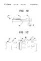
- FIG. 1Ais an exploded perspective view of a disk drive embodying the invention.
- FIG. 1Bis a side view of the disk drive of FIG. 1 A.
- FIG. 1Cis a plan view of a portion of the disk drive of FIG. 1A, together with a cable for connecting the disk drive to a host system.
- FIG. 1Dis an overall functional block diagram of the disk drive of FIG. 1 A.
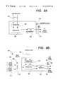
- FIG. 2Ais a drawing of a disk surface having a plurality of tracks arranged in a prior art embedded servo format.
- FIG. 2Bis a drawing of a disk surface having a plurality of tracks arranged in an embedded servo format in accordance with a preferred embodiment of the invention.
- FIG. 2Cis an enlarged view of a fragment of the disk surface of FIG. 2 B.
- FIG. 3Ais a diagram of a servo track segment having a format in accordance with a preferred embodiment of the invention.
- FIG. 3Bis a diagram of a data track segment having a format in accordance with a preferred embodiment of the invention.
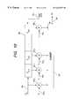
- FIG. 4is a block diagram of a suitable implementation of channel 26 of FIG. 1 D.
- FIG. 5is a block diagram of a suitable implementation of read channel 200 including associated register set 122 of FIG. 4 .
- FIG. 6is a block diagram of a data detection circuit employing MLSE data detection, which has suitable structure to implement circuit 242 of FIG. 5 .
- FIG. 7is a block diagram of a suitable implementation of shared sync mark detecting stucture including circuitry in the read path of ENDEC circuit 246 of FIG. 5 .
- FIG. 8Ais a block diagram of a suitable implementation of circuitry in the write path of ENDEC circuit 246 of FIG. 5 .
- FIG. 8Bis a block diagram of a suitable implementation of RLL decoder 391 of FIG. 7 .
- FIG. 9Ais a block diagram of a suitable implementation of a shared pattern detector 380 of FIG. 7 .
- FIG. 9Bis a block diagram of an embodiment of an i-of-m comparator 410 that employs a digital bit summing circuit and is suitable for use in shared pattern detector 380 of FIG. 7 .
- FIG. 9Cis a block diagram of an embodiment of an i-of-m comparator 410 that employs an analog summing circuit and is suitable for use in the shared pattern detector 380 of FIG. 7 .
- FIG. 10is a block diagram of a suitable implementation of an equalizer 336 suitable for use in data detection circuit 242 shown in FIG. 6 .
- FIG. 11Ais a state diagram of the state trapping control flow for channel 26 of FIG. 1 D.
- FIG. 11Bis a timing diagram showing the relationship between servo gate (SGATE), read gate (RGATE), burst gate (BGATE) and information recorded in a disk track segment.
- SGATEservo gate
- RGATEread gate
- BGATEburst gate
- HDDHARD DISK DRIVE
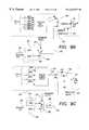
- a hard disk drivein accordance with a preferred embodiment of the invention includes a head disk assembly (“HDA 10 ”) and a printed circuit board assembly (“PCBA 12 ”).
- HDA 10head disk assembly
- PCBA 12printed circuit board assembly
- HDA 10includes a suitable number of magnetic disks 14 (two disks being shown in FIG. 1 A), a pivot bearing cartridge 15 , a spindle motor 16 , a voice coil motor (“VCM 18 ” in FIG. 1 D), a head stack assembly (“HSA 19 ”), and a plurality of permanent magnets 21 for VCM 18 .
- HSA 19includes a coil 23 , an actuator frame 27 , and a suitable number of head gimbal assemblies each including a transducer suspension 13 and a slider or head that includes a read transducer 20 .
- a suitable read transduceris an inductive transducer.
- a magneto-resistive (“M”) transduceris also suitable; a slider containing an MR transducer for reading generally also includes an inductive transducer for writing.
- HSA 19also suitably includes a flex circuit assembly that includes a flex circuit 29 , a preamplifier (“preamp 22 ”), a plurality of passive electrical components that include resistors, capacitors, connectors, and suitable mounting hardware.
- PCBA 12includes a printed circuit board (“PCB 31 ”) and a plurality of integrated circuits (“ICs 500 ”), some of which are disposed on one side of PCB and others of which are disposed on the opposite side of PCB 31 .
- PCBA 12further includes a plurality of active and passive electrical components, and connectors for connecting PCBA 12 to HDA 10 and to a host system (the host not being shown).
- PCBA 12includes a connector 52 which interfaces with a matching host connector 522 which couples to a host I/O interface or I/O bus adapter via an I/O cable 520 .
- connector 52is a 40-pin EIDE connector that conforms to certain ANSI interface standards.
- the host interface connectionmay be designed to be compatible with any other suitable host interface.
- PCBA 12is suitably affixed to HDA 10 by screws which are received by matching threaded openings in HDA 10 .
- PCBA 12may be affixed to HDA 10 through adhesive bonding, press snap fitting, or other methods.
- PCBA 12is suitably electrically connected to HDA 10 via a connector 540 and a connector 542 .
- Connector 540connects circuitry in PCBA 12 to preamp 22 , coil 23 and spindle motor 16 in the interior of HDA 10 .
- Connector 540suitably is a plug connector; it may be some other kind of connector such as a zero insertion force (ZIF) flex circuit connector.
- Connector 542connects windings of spindle motor 16 to circuitry in PCBA 12 .
- connection 540 and 542may be suitable for attaching to a commercially available HDA.
- the details of a suitable HDAare shown in U.S. Pat. No. 5,270,887, the disclosure of which is incorporated by reference.
- HDA 10includes two motors, i.e., spindle motor 16 and voice coil motor (“VCM 18 ”).
- Spindle motor 16is mechanically coupled to cause disks 14 to rotate.
- VCM 18is implemented by structure shown in FIG. 1A including magnets 21 and portions of HSA 19 such as coil 23 .
- disks 14provide four recording surfaces. Each of the recording surfaces has a plurality of tracks arranged an embedded servo format.
- an embedded servo formatincluding the format employed in a preferred embodiment, there are provided interspersed servo-data regions and user-data regions; each servo-data region includes servo track segments for storing servo data and servo bursts, and each user-data region includes user track segments for storing user data.
- Each of a suitable number of transducers 20provides for reading and writing with respect to a respective one of the recording surfaces of disks 14 .
- Alternative embodimentsmay have more or fewer disks.
- each transducer 20When reading, each transducer 20 generates a low level analog read signal 17 , which for inductive heads and many MR heads is a differential signal. Analog read signal 17 is conveyed to signal inputs of preamp 22 . Preamp 22 produces a read signal 24 which is an amplified, differential, analog read signal. HDA 10 also includes a path for conveying read signal 24 to PCBA 12 ; a path for conveying a write data signal 28 to preamp 22 ; and a path for conveying preamp control signals 30 for preamp 22 . Under control of control signals 30 , preamp 22 operates in either a read mode or a write mode and in either case communicates with a selected transducer 20 . Suitably, preamp 22 is implemented by a commercially available IC such as the SSI 32R2202 or SSI 32R2203, each of which is manufactured by Silicon Systems Inc., Tustin, Calif.
- spindle motor 16is a multi phase, brushless DC motor.
- the prior artteaches suitable means for controlling spindle motor 16 to spin up to, and down from, a substantially constant angular velocity.
- VCM 18is an element of a head-positioning servo system, and applies torque to HSA 19 to swing it during a track-seeking operation and to maintain it at a desired angular position during a track-following operation.
- preamp 22provides write current to a selected transducer 20 ; the write current changes polarity upon each change in binary value of write data signal 28 .
- Read signals 17 and 24have the same information content, and both are noise-corrupted.
- a selected transducer 20 and preamplifier 22constitute a read means operative during a user-data read operation for reading data from the disk surface to produce a time-multiplexed analog read signal that during a revolution of the disk represents servo data during each of one set of time intervals; represents servo bursts during each of another set of time intervals; and represents user data during each of another set of time intervals.
- PCBA 12includes a channel 26 and a host interface and disk controller (“HIDC 32 ”), each of which preferably is implemented as a single IC.
- these two ICsin combination perform overall functions including basic timing functions that in certain prior art disk drives three ICs had performed.
- One such basic timing functionentails the generation of the “global clock” and the synchronization of the global clock to the servo sample rate.
- One of the 3 ICs within such prior art disk drivesis a servo IC, the other 2 being a channel IC and a disk controller IC, with the servo IC containing circuitry for generating and synchronizing the global clock.
- IDC 32contains circuitry for generating the global clock which is synchronized to the servo sample rate by a signal supplied by channel 26 .
- HIDC 32contains timing circuitry controlled by the global clock to provide timing signals used in de-multiplexing including separating servo data from servo bursts and from user data.
- channel 26includes the global clock and timer circuitry.
- channel 26provides, among other things, a signal processing path for processing read signal 24 to produce a clocked, serial-by-symbol data signal (i.e., a decoded binary data signal and accompanying clock signal).
- a signal processing pathfor processing an analog read signal produced by a preamplifier to produce such a clocked serial-by-symbol data signal is commonly called a “read channel.”
- Channel 26also provides a signal processing path for processing a clocked serial-by-symbol data signal provided by HIDC 32 to produce a serial-by-bit data signal for the analog signal input of preamp 22 .
- serial-by-symbol data signalspropagate between channel 26 and HIDC 32 via a channel data bus 38 .
- the clock signals for the serial-by-symbol data signalsare shown collectively as NRZ CLOCKING 41 in FIG. 1 D.
- timing recovery circuitis commonly employed in read channels.
- Such a timing recovery circuitgenerally has a lock to reference mode, an acquisition mode and a tracking mode. During each such mode, the timing recovery circuit produces an oscillating signal which is locked onto the same, or substantially the same, frequency as an oscillating signal it receives as an input.
- the oscillating signal input to the timing recovery circuitis the output of a frequency synthesizer.
- the oscillating signal input to the timing recovery circuitis read signal 24 .
- Certain properties of the timing recovery circuitare modified between acquisition mode and tracking mode; these include loop gain and other properties affecting bandwidth and stability.
- Channel 26is coupled to receive read signal 24 through a set of coupling capacitors 25 and has a port 40 connected via bus 38 to an NRZ port 45 in HIDC 32 .
- Ports 40 and 45 and interconnecting bus 38propagate data in a clocked, serial-by-symbol form referred to herein as non-return-to-zero (NRZ) form.
- NRZnon-return-to-zero
- the terms “NRZ” and “NRZI” (Non-Return to Zero Inverted) as used hereinhave their customary meaning in this art.
- NRZrefers to a coding system in which a binary 1 is represented (at an instant in time indicated by a clock signal) by a 1st level or state and a binary 0 is represented (at an instant in time indicated by a clock signal) by a second level or state.
- NRZIrefers to such a clocked coding system in which a binary 1 is represented by a transition from a 1st level or state to a second level or state and a binary 0 is represented by the absence of a transition.
- channel 26processes read signal 24 to produce, on port 40 , a clocked serial-by-symbol data signal that sequentially represents the same servo data and the same user data that the analog read signal represents.
- channel 26supports use of a partial response, maximum likelihood (PRML) coding system.
- PRMLrefers to a type of signal processing employing sampled and equalized values of an input signal which are evaluated over several samples to estimate symbols contained in the input signal. PRML is one type of a broader class of signal processing systems referred to as “sampled-data processing systems.”
- HIDC 32performs numerous control functions for the disk drive including host interface functions to manage transfer of data between the disk drive and the host, and certain disk controller functions to manage the operation of channel 26 in writing and reading data.
- HIDC 32has circuitry for producing certain tiing and control signals that are part of a set identified collectively as timing and control signals 44 which are sent between channel 26 and HIDC 32 .
- timing and control signals 44As part of timing and control signals 44 , HIDC 32 sends to channel 26 one of a set of signals collectively identified as write gate signal (WGATE) and one of a set of signals collectively identified as read gate signal (RGATE).
- HIDC 32sends to channel 26 as part of timing and control signals 44 one of a set of signals collectively identified as burst gate signal (BGATE), and one of a set of signal identified as AM ENABLE.
- BGATEburst gate signal
- AM ENABLEone of a set of signal identified as AM ENABLE.
- HIDC 32includes sector timer circuits, and channel 26 sends a SYNC DET signal 46 and an AM DET signal 47 to HIDC 32 to synchronize the sector timer circuits.
- channel 26includes sector timer circuits synchronized by SYNC DET signal 46 and AM DET signal 47 , obviating the need to send these signals to HIDC 32 .
- channel 26internally produces BGATE and AM ENABLE, obviating the need for HIDC 32 to send a BGATE signal or an AM ENABLE signal to channel 26 .
- the “SYNC DET” signalis a particular data word conveyed via NRZ bus 38 rather than a binary-valued signal carried by a single line. These two implementations are functionally equivalent. In each case, the signal informs HIDC 32 that channel 26 has detected the sync word.
- PCBA 12also includes a data buffer 42 , a microprocessor 34 , a read only memory (“ROM 54 ”), a writeable random access memory (“RAM 60 ”), a VCM driver 58 for supplying current to VCM 18 , and a spindle motor driver 56 for supplying current to spindle motor 16 .
- PCBA 12also includes a host interface bus 50 for conveying commands and data between HIDC 32 and the host, a microprocessor bus 36 , a buffer bus 48 for conveying data between HIDC 32 and data buffer 42 , and a path for conveying control signals 30 that provide for bi-directional control interactions between preamp 22 and HIDC 32 .
- microprocessor 34is a commercially available microprocessor or microcontroller, such as Model No. 80C196NP2 available from Intel Corporation.
- Microprocessor 34executes instructions acquired from a stored control program to control disk drive functions. These functions include reading and decoding host commands, starting up and controlling the speed of spindle motor 16 , minimizing head-positioning servo off track error through control of VCM 18 , managing reduced power modes of operation, and other disk drive functions.
- Microprocessor 34includes an I/O port that is connected to microprocessor bus 36 .
- Microprocessor 34suitably includes an embedded ROM that stores some of the control programs it uses.
- control programsinclude the instructions microprocessor 34 executes, and tables, parameters or arguments used during the execution of these programs.
- Microprocessor control programsmay also reside in any or all of ROM 54 , RAM 60 , or data buffer 42 .
- Microprocessor 34may also include a register set and may also include a writeable random access memory (RAM).
- Microprocessor 34suitably has separate ports for directly communicating with spindle motor driver 56 and VCM driver 58 .
- Channel 26has a port 120 and HIDC 32 has a port 35 that connect to microprocessor bus 36 , whereby microprocessor 34 is capable of communicating directly with either IC via microprocessor bus 36 .
- Microprocessor bus 36also enables microprocessor 34 to communicate directly with ROM 54 , and RAM 60 .
- spindle motor driver 56 and VCM driver 58may be connected to a single port or to microprocessor bus 36 .
- Channel data bus 38includes an 8-bit wide (byte-wide) parallel path, alternate embodiments may employ more or fewer parallel bits for channel data bus 38 . Depending upon applicable data transfer requirements, a 4-bit wide (nibble-wide) path or even a serial-by-bit path may be suitable for channel data bus 38 .
- channel 26with connections to both microprocessor bus 36 and channel data bus 38 enables microprocessor 34 and channel 26 to communicate via microprocessor bus 36 without interfering with high speed read/write data exchange between channel 26 and HIDC 32 via channel data bus 38 .
- channel 26includes circuitry to accept write data from HIDC 32 via channel data bus 38 and port 40 , to encode write data, and to produce write data signal 28 which is conveyed via preamp 22 to selected transducer 20 .
- channel 26encodes write data in accordance with Run Length Limited (RLL) code constraints.
- RLLRun Length Limited
- RLLrefers to a type of coding which restricts the minimum and maximum number of binary zeros between binary ones.
- Channel 26also includes circuitry to process read signal 24 , and, on a time-muitiplexed basis, generate decoded digital user data, decoded digital servo data, and a digital representation of demodulated servo burst data.
- the decoded digital servo data and decoded digital user dataare conveyed to HIDC 32 via port 40 , channel data bus 38 , and HIDC NRZ port 45 .
- Microprocessor 34acquires the demodulated servo burst data via microprocessor port 120 and microprocessor bus 36 , and uses these data to perform fine-position head-positioning servo operations.
- An alternative embodimentmay incorporate servo control circuitry in a servo IC in which case the demodulated servo burst data would be provided to such IC.
- HIDC 32includes a buffer port 37 connected to buffer bus 48 , and host interface port 33 connected to host-interface bus 50 .
- HIDC 32includes a buffer manager-arbitrator circuit that manages access to data buffer 42 and manages bi-directional exchange of data between HIDC 32 and data buffer 42 via buffer bus 48 .
- Host interface port 33provides for communicating with the host via host interface bus 50 and host connection 52 .
- host interface port 33includes a set of ATA compatible host interface task file registers implemented as taught in the prior art. Both microprocessor 34 and other circuitry within HIDC 32 can read task file register contents.
- This preferred host interface port 33also includes a set of host command registers and host data registers for parallel transfer of commands and data via host interface bus 50 .
- HIDC 32also controls disk formatting and address translation.
- the translating of addressesincludes translating a logical block address to a cylinder/head/sector address and provides for defect management.
- HIDC 32also includes error detection and correction (EDAC) circuitry that is used to correct errors in user data that were read from disks 14 and stored in data buffer 42 .
- EDACerror detection and correction
- Data buffer 42is implemented as random access memory such as a dynamic random access memory (DRAM) or a static random access memory (SRAM).
- DRAMdynamic random access memory
- SRAMstatic random access memory
- data bufferis implemented by at least one DRAM or SRAM IC that is affixed to PCB 31 .
- data buffer 42 and buffer bus 48may be incorporated into HIDC 32 .
- Data buffer 42stores data recovered from a disk 14 , data provided by the host that are to be recorded on a disk 14 , and, optionally, disk drive commands, servo data and control programs for microprocessor 34 .
- the buffer manager within HIDC 32arbitrates access to data buffer 42 when contention for access to data buffer 42 occurs as consequence of various concurrent operations.
- Disk drive commands received from the hostmay be stored in data buffer 42 and be subsequently retrieved by microprocessor 34 .
- ROM 54is an optional conventional IC that stores at least part of the control program used by microprocessor 34 . ROM 54 may be omitted in an embodiment in which microprocessor 34 includes embedded ROM suitable for replacing the functions of ROM 54 .
- RAM 60is an optional, conventional RAM IC used to enlarge the high speed writeable memory available to microprocessor 34 .
- RAM 60is included in PCBA 12 when microprocessor 34 lacks sufficient internal RAM, and data buffer 42 cannot provide microprocessor 34 sufficient external storage or sufficiently fast external storage.
- the hostmay be any electronic device that has an input/output (I/O) bus and interface connection means that is compatible with host connection 52 , host interface bus 50 and host interface port 33 .
- the hostmay be a personal computer that includes an AT bus which has become a de facto standard for EBM PC compatible computer systems and is referred to as the Industry Standard Architecture (ISA).
- ISAIndustry Standard Architecture
- a higher speed Enhanced AT bushas also been introduced.
- Various attachments to the AT bushave also become common for allowing peripherals, including disk drives, to more efficiently couple to the AT bus.
- the Integrated Drive Electronics (IDE) attachment to the AT bushas become a very common interface for attaching disk drives to the standardized AT bus and is commonly referred to as the ATA (for AT bus Attachment) standard.
- IDEIntegrated Drive Electronics
- an interface standard referred to as Enhanced IDEis used to couple disk drives in the host.
- the disk driveis adapted to attach to the host I/O bus via an EIDE connector.
- connection 52may be implemented for connecting directly to a host I/O bus.
- Alternative disk drive embodimentsmay conform to other interface specifications and appropriate other connections may be employed.
- Such alternate interfacesinclude the Small Computer Standard Interface (SCSI), the Serial SCSI Architecture (SSA) interface, the P 1394 interface, the Fiberchannel interface, and the parallel printer port interface.
- SCSISmall Computer Standard Interface
- SSASerial SCSI Architecture
- P 1394the P 1394 interface
- Fiberchannel interfacethe Fiberchannel interface
- parallel printer port interfacethe serial printer port interface
- each disk 14preferably has two data-storage surfaces. Each of these surfaces has a plurality of concentric tracks arranged in an embedded servo format including a plurality of radially-extending user-data regions 62 and a plurality of radially-extending servo-data regions 64 .
- Servo-data regions 64are written by a servo writer under controlled conditions. In FIG. 2B, the angular size of each servo-data region 64 is greatly exaggerated, and only five such regions are shown. The number of servo-data regions required depends on various factors; typically they number between 60 and 100 with a number as low as 10 and as high as 150, or more, also being suitable.
- the term “user data”refers to information recovered from or to be written into user-data regions 62
- servo datarefers to information recovered from servo-data regions 64 .
- the radial terminus (or arc-shaped boundary) of each data zone band, D iis a data zone boundary 67
- the radial terminus (or arc-shaped boundary) of each servo zone band, S iis a servo zone boundary 63 .
- Each data zone band, D iincludes a plurality of data track segments 90 (FIG.
- each servo zone band, S iincludes a plurality of servo track segments 68 (FIG. 3A) each of which has servo data recorded therein at a single channel frequency with channel frequency varying from servo zone band to servo zone band.
- data track segment and servo track segmentrefer to the elements that make up a complete track; each data track segment 90 is located between consecutive servo-data track segments 68 .
- channel frequencyas used herein has its customary meaning in this art.
- the channel frequencyis the reciprocal of a time period “T,” where the “T” is the time period consumed while an elemental-length magnet passes under the transducer during a read operation with the disk spinning at a constant angular velocity.
- the length of each magnet recorded along a track as a result of a write operationis, to a first order of approbation, either an elemental length or an integer multiple of the elemental length.
- Channel 26operates at the same channel frequency during read operations for every data track segment 90 in the same data zone band; similarly, channel 26 operates at the same channel frequency during read operations for every servo track segment 68 in the same servo zone band.
- Varying the channel frequency from zone band to zone bandhas an advantage in that it promotes ma izing bit density within tolerated error constraints. Selection of channel frequency is determined by the linear track length, transducer flying height, media quality (e.g., disk surface smoothness, quality of the magnetic coating material, etc.) and constraints imposed by channel 26 . Typically, the channel frequency will increase in an outward radial direction. For data zone bands, the channel frequency of innermost zone band D 1 is less than the channel frequency of zone band D 2 , which is less than the channel frequency of zone band D 3 . . . which is less than the channel frequency of outermost zone band D M .
- the channel frequency of innermost zone band S 1is less than the channel frequency of zone band S 2, which is less than the channel frequency of zone band S 3 . . . which is less than the channel frequency of outermost zone band S N .
- This increase in channel frequency from zone band to zone bandallows linear bit density to be maintained at or near an optimal level while moving from inner to outer tracks.
- Servo zone bands S 1 -S Npreferably share the same zone boundaries as data zone bands D 1 -D M , as shown in FIG. 2B, but need not do so in alternative embodiments.
- fewer servo zone bands than data zone bandsare defined in the format, as shown in FIG. 2B.
- a suitable number of data zone bandsis as low as 2 and as high as 20, or more.
- the number of zone bands usedwill vary with the specific disk drive implementation.
- FIG. 2Billustrates a format having more data zone bands than servo zone bands, alternatively, the number of servo zone bands N may be greater than the number of data zone bands M.
- At least two servo zone bands and at least three data zone bandsare provided.
- the upper limit to the number of zone bandsis only limited by the number of tracks on a disk surface.
- a guard bandconsisting of one or more unused data tracks is provided between servo zone bands to avoid intertrack interference.
- the guard bandswill include at least two tracks, one guard track for each zone band, with the guard track containing valid servo data consistent with the zone band that it guards.
- the use of guard bandslimits the number of servo zone bands to be substantially less than the total number of tracks on the disk surface.
- zone bandsin which a servo track segment 68 and immediately following data track segment 90 have different channel frequencies.
- channel 26While processing read signal 24 during a user-data read operation, channel 26 needs to switch from one channel frequency to another and back again in a repeating fashion as user-data regions and servo-data regions pass under selected transducer 20 .
- Such frequenciesmay be substantially different, e.g. differing from 10% to 100%.
- a suitable signal-processing meansis necessary.
- channel 26incorporates a read channel 200 (FIG.
- Such a read channelmay include duplicated signal paths for user data processing and servo-data processing.
- the zone to zone frequency changeneed not be the same from zone band to zone band, and the number of tracks within a zone band may change from zone band to zone band. For example, fewer tracks may be provided in the outer zone bands than the inner zone bands.
- zoned servo-data regions 64when compared with a constant frequency servo wedge approach, is that using higher linear bit densities in the outer zone bands enable the allocation of less disk area to the servo-data regions.
- a constant frequency servo wedge approachemploys servo wedges that are significantly wider at the outermost part of the disk surface than they are at the innermost part of the disk surface.
- each servo-data region 64has a step wise decreasing angular shape as zone bands at larger disk radii are considered.
- a pair of dashed lines defining a simple wedge shapeindicates the area which would be occupied by a servo-data region in the case of a constant frequency servo wedge approach.
- zoned servoreduces the disk area consumed by servo data, and thereby increases the available disk surface area for user-data regions 62 a and 62 b on opposite sides of a given servo-data region 64 .
- This additional surface space available for data storageis shown as region-a 66 a and region-b 66 b in FIG. 2 C.
- servo-data regions 64make more feasible use of a larger number servo-data regions 64 (e.g. up to 150 or more). Increasing the number of servo-data regions 64 facilitates use of higher servo sample rates which in turn permits use of higher track densities. Alternatively, if the number of servo-data regions 64 is maintained constant (i.e., relative to a non-zoned servo approach), the zoned servo approach increases the disk area available for storing user data, as shown in FIG. 2 C. In either case, use of zoned servo enables increasing the user-data storage capacity realized from disk 14 . This increase in efficiency is offset to a small degree by the need to use one or more guard band tracks at each servo zone boundary 63 .
- Every servo track segment 68has a servo sector sync mark (“SSM 76 ”).
- SSM 76is a track-independent data string defining a predetermined servo-sync mark. Every SSM 76 within a given servo-data region 64 is arranged in alignment with an alignment radius 61 (FIG. 2 C). Each servo-data region 64 has its own alignment radius 61 . Preferably, in accordance with another invention made by the assignee hereof, the end of each SSM 76 is aligned with alignment radius 61 . Alternate embodiments may align some other servo-data field with alignment radius 61 .
- Detection of SSM 76causes channel 26 to issue SYNC DET 46 to HIDC 32 which precisely establishes a timing reference point for any read/write operations that occur until the next SSM 76 arrives. After being synchronized with one SSM 76 arrival time, timers in HIDC 32 predict subsequent SSM 76 arrival times.
- the angular separation between adjacent alignment radii 61is the same for all alignment radii 61
- the time interval between SSM 76is the same for all SSM 76 on a single disk surface and does not change during track-seeking operations that traverse a servo zone boundary 63 (FIG. 2 C), and, consequently, servo fiming need not be adjusted during track-seeking operations. If any servo field element other than SSM 76 were to be aligned with alignment radius 61 , the SSM field would not be aligned from zone band to zone band and, it would not be possible to maintain constant servo sector SYNC DET timing during track-seeking operations that cross zone boundaries.
- a complete servo track segment 68 in a servo-data region 64includes the fields shown diagrammatically in a straight line.
- all servo-data track segments 68are similar and each includes the fields shown in FIG. 3 A.
- servo track segment 68provides fields for storing the following elements, in sequence, an automatic gain control bit stream (“AGC 70 ”), a servo address mark (“SAM 72 ”), a preamble or phase lock loop bit stream (“PLL 74 ”), SSM 76 , a cylinder address referred to herein as TRK ID 78 , a redundant TRK ID 79 , a servo sector address (“SSA 80 ”) that includes a servo sector number and head number, a redundant servo sector address (“redundant SSA 82 ”) that also includes a servo sector number and head number, a cyclical redundancy check code (“CRC 84 ”), a redundant CRC 85 , PADA 88 a , servo bursts 86 (e.g. 2-6 bursts) used primarily for track following
- AGC 70automatic gain control bit stream
- SAM 72servo address mark
- PLL 74preamble or phase lock loop bit stream
- SAM group 71 aincludes AGC 70 and SAM 72 fields and elements
- servo ID group 71 bincludes PLL 74 , SSM 76 , TRK ID 78 , redundant TRK ID 79 , SSA 80 , redundant SSA 82 , CRC 84 and redundant CRC 85
- servo bursts group 71 cincludes servo bursts 86 and PAD 88 .
- the SAM group 71 aenables channel 26 to locate the beginning of a servo track segment 68 when servo sector timers cannot be used to do so.
- AGC 70is a constant-frequency bit stream that has sufficient length to enable an automatic gain control (AGC) circuit in channel 26 to establish a desired signal level within channel 26 before SAM 72 passes under the selected transducer 20 .
- AGCautomatic gain control
- the use of AGC amplifiersfacilitates reducing the read error rate of channel 26 while recovering data and consequently reduces the SAM 72 misdetection rate.
- Using AGCincreases the signal to noise ratio in channel 26 while processing any track element and improves channel 26 performance in other ways.
- SAM 72is used during a disk drive calibration procedure that synchronizes servo sector timers with the time that SSM 76 arnives at the selected transducer 20 .
- the servo sector timersare subsequently used to predict the arrival of other track elements and to initiate the associated processing of these elements.
- SSM 76 arrival timesmay vary because of variations in the speed of rotation of disks 14 .
- the calibration processreads the information recorded on the disk surface and searches for a SAM 72 ; upon detecting a SAM 72 , channel 26 issues AM DET 47 to indicate the arrival of a PLL 74 and the imminent arrival of the associated SSM 76 .
- the subsequent arrival and detection of SSM 76causes channel 26 to issue SYNC DET 46 ;
- SYNC DET 46serves as a timing reference and synchronizes servo sector timers.
- the preferred SAM 72 codesviolate the RLL code constraints employed during recording of all other servo and user data.
- a primary consideration in the selection of a preferred SAM 72 bit patternis that it be easily distinguished from all other information recorded on the disk surface.
- the information recorded in servo ID group 71 b for each servo track segment 68is unique, and when read identifies the particular disk surface, servo-data region 64 , and track that is being processed.
- Channel 26processes the information defined in serial-by-bit form by servo ID group 71 b , converts it to NRZ data and sends the NRZ data to HIDC 32 via channel data bus 38 .
- Microprocessor 34acquires these data by reading registers contained in HIDC 32 .
- HIDC 32 and microprocessor 34use the servo data to confirm the identity of transducer 20 and disk surface being read, and to determine the radial and angular position of selected transducer 20 over the selected disk surface.
- PLL 74is a sequence of bits recorded at a constant frequency, and has a sufficient number of consecutive flux reversals to enable circuitry in channel 26 to achieve phase synchronization with PLL 74 before SSM 76 arrives at the selected transducer 20 . Suitable means for achieving this bit synchronization are taught in the prior art.
- Channel 26also uses SSM 76 to locate the first bit in TRK ID 78 , servo-data framing, as further discussed below.
- SSM 76conforms to the same RLL code constraints used to encode user data.
- SSM codesare selected to be robust in the sense that they facilitate the design of detection logic that is able to precisely locate SSM 76 despite the channel having read one or more code bits of SSM 76 in error. Robust codes are further discussed below.
- TRK ID 78has the same bit pattern for all servo-data track segments 68 in a given track, and has a different bit pattern for every track on the same disk surface.
- TRK ID 78is a track-dependent data string for uniquely identifying the track involved in a read operation.
- the preferred servo track segment 68also includes an optional redundant TRK ID 79 .
- both TRK ID 78 and redundant TRK ID 79are Gray coded bit patterns, and are phase coherent.
- Gray codeas used herein has its customary meaning in this art. That is, a Gray-coded track-identifyig string is such that only one logical bit of the string changes from a track to either adjacent track.
- TRK ID 78 and redundant TRK ID 79being phase coherent, this relates to the phases of flux reversals of TRK ID patterns written in radially adjacent tracks.
- phase coherencyis achieved through use of tri-bit encoding.
- each logical bitsuch as a logical bit of a Gray-coded track ID is represented by a codeword having three code bits, with each code bit being represented by the presence of a flux reversal (of either polarity; i.e., either a positive-polarity flux reversal [“+”] or a negative-polarity flux reversal [“ ⁇ ”])or by the absence of a flux reversal [“0”].
- phase coherencymeans that the first flux reversals in adjacent codewords on adjacent tracks have the same polar.
- Phase coherencymay not be maintained at servo zone boundaries 63 (FIG. 2 C).
- the optional redundant TRK ID 79when present, improves track detection reliability and reduces the probability that track ID errors will occur during track-seeking operations; this advantage is particularly significant when very high bit densities are used to record servo track segment 68 in disk drives that use high speed track-seeking operations.
- SSA 80 and redundant SSA 82are codes that are unique in each servo-data region 64 in the disk drive, i.e., these codes are defined so that they may be used to uniquely identify the transducer 20 and disk surface being used (assuming more than one disk surface containing data are provided) and the specific servo-data region 64 that is passing under the transducer 20 .
- codesmay be implemented in any of a variety of ways; for example, they may be implemented as a single value that is different for each servo-data region 64 in the disk drive, as a unique value for each servo track segment 68 in the disk drive or, preferably, as a pair of values that separately identify which transducer 20 and disk surface is being used and which servo-data region 64 on a disk surface is under the selected transducer 20 .
- SSA 80 and optional redundant SSA 82are preferably provided to facilitate headerless data sector formats; i.e., where the header information conventionally provided in front of each data sector is omitted and the necessary information for locating data sectors is acquired instead from servo track segment 68 . Eliminating data sector ID fields and using servo embedded information to locate user-data sectors enables making more of the disk surface available for recording user data.
- Servo track segment 68preferably includes a cyclical redundancy check code (“CRC 84 ”) and an optional redundant CRC 85 which provides error detection for the servo data recorded in servo track segment 68 .
- CRC 84preferably provides read error checking for TRK ID 78 and SSA 80 while redundant CRC field 85 preferably provides read error detection for redundant TRK ID 79 and SSA 82 .
- PADA 88 aserves to isolate servo bursts 86 from CRC 84 or redundant CRC 85 and thereby reduces intersymbol interference.
- PADA 88provides time margin for changing the read mode of channel 26 at the end of servo ID group 71 b.
- Servo burst 71 c groupparticipates in the operation of the head-positioning servo system to maintain the selected transducer 20 at or near a hypothetical disk track centerline during track-following operations.
- bursts 88consist of a sequence of some 2 to 8 short bursts that are radially displaced about the track centerline in a conventional manner to the end that playback signal amplitude for each short burst depends upon the radial position of the selected transducer 20 relative to the short burst that is being processed.
- Servo track segment 68also includes a PADB 88 b which serves to isolate servo bursts 86 from recorded information that follows bursts 88 .
- PADB 88 balso provides time margin for changing the read mode of channel 26 at the end of servo burst 88 .
- SSA 80 and 82 and CRC 84 and 85need not be Gray coded or be written in a phase coherent manner since such data are not employed during track-seeking operations.
- the transition from TRK ID 78 or 79 to SSA 80may be separated by an intervening gap (not shown) included to reduce intersymbol interference between the adjacent phase coherent field ( 78 or 79 ) and phase incoherent field 80 .
- a data track segment 90 in a user-data region 62includes the fields shown diagrammatically in a straight line.
- Each data track segment 90is made up of at least one and as many as 10 or more data sectors 92 , begins at the end of a servo track segment 68 (shown as 68 a in FIG. 3 B), and ends at the beginning of the next servo track segment 68 (shown as 68 b in FIG. 3B) .
- the representative data track segment 90 shown in FIG. 3Bincludes two data sectors 92 a and 92 b .
- each data sectorhas the same format as one of the data sectors 92 a or 92 b .
- One or more of the data sectors 92 in a given data track segment 90may be partial data sectors or split data sectors as further discussed below.
- Each data sector 92may start with an AGC bit stream such as AGC 96 a in data sector 92 a and AGC 96 b in data sector 92 b .
- Each data sector 92may include an Error Detection And Correction code such as EDAC 101 a in sector 92 a .
- Each data sector 92preferably has fields storing the following elements: a data PLL bit stream (“PLL 98 a ” in sector 92 a , “PLL 92 b ” in sector 92 b ), a data sync mark (“DSM 100 a ” in sector 92 a , DSM “ 100 b ” in sector 92 b ), user-data record (“USER DATA 94 a ” in sector 92 a , “USER DATA 94 b in sector 92 b ), and a data pad CAD 106 a in sector 92 a , “PAD 106 b ” in sector 92 b ).
- Alternate embodimentsmay include additional fields.
- an EDAC 101need not be included in all data sectors 92 .
- AGC 96 and PLL 98play the same roles for a data sector that AGC 70 and PLL 74 do for a servo segment. That is, AGC 96 is a constant-frequency bit stream having sufficient length to enable an AGC circuit in channel 26 to establish a desired signal level within channel 26 before DSM 100 arrives at the selected transducer 20 .
- PLL 98is a sequence of bits recorded at a constant frequency which has a sufficient number of consecutive flux reversals to enable timing circuitry in channel 26 to achieve phase synchronization before DSM 100 arrives at the transducer 20 .
- AGC 96 and PLL 98may be considered to be a single field that provides for overlapped AGC operation and timing circuit phase alignment.
- Each DSM 100participates in framing user data within channel 26 to locate the first bit in its user-data record 94 and to establish byte boundaries for an ENcoding And DECoding circuit (“ENDEC circuit 246 ” shown in FIG. 5 ).
- ENDEC circuit 246ENcoding And DECoding circuit 246
- a primary consideration in selecting a bit pattern for DSM 100is that it be robust in the sense that it can be recovered (identified) despite the presence of noise in the playback signal that causes one or more bits in DSM 100 to be read incorrectly.
- DSM 100 and SSM 76are different robust codes.
- Most user-data records 94store a fixed sized quantity of data called a “logical sector” or “logical block” as supplied to the disk drive via host interface bus 50 (FIG. 1 D).
- Typical logical block sizesare 512, 1024 or 2048 bytes with 512 bytes being the preferred length for most hard disk drives.
- the amplitude of read signal 17(FIG. 1D) is affected by the frequency content of the information being read and how well transducer 20 is registered over data sector 92 being read.
- Successive data sectors 92 in the same data track segment 90may be written at different times while the disk drive is subjected to different operating environments with the result that successive data sectors 92 are written at slightly different radial positions.
- data stored in successive recordsmay be different with the result that the frequency content of the playback signals is different. Accordingly, all data sectors 92 include PLL 98 .
- every data sector 92has the same fixed size user-data record 94 length that equals the preferred logical block length, e.g., 512 bytes.
- design optimization of a given disk drive that employs both embedded zoned servo and zoned data recordingusually forces a compromise between the physical length of a data track segment 90 and user-data record 94 length in one or more data zone bands. The compromise is forced by a need to provide adequate disk surface resources to the head-positioning servo system while allowing user data to be recorded at the maximum linear bit density and thereby to realize the maximum storage capacity for the disk drive.
- the preferred method for making this compromiseis to split a complete logical block into two parts and store the two parts in successive user-data records 92 , a logical pair of split data sectors 92 .
- a split user-data record 94may have any length that is less than the length of a logical block provided that a logical pair of split data records 92 store a complete logical block.
- Split user-data record 94 lengthis selected to permit recording the entire data track segment 90 at the highest linear recording density usable in the data zone band.
- a given trackmay use any number of split user-data record 94 lengths, in preferred implementations, two split user-data record 94 lengths are chosen for use in all split data sectors in a given data zone band.
- a split data record 92 b that contains the first part of a split logical blockmay terminate at the beginning of a servo track segment 68 b in which case, the first user-data record following the servo track segment 68 b will be a split data sector 92 that contains the second part of the split logical block.
- the split data sectorsare said to swallow the servo track segment 68 b .
- split data sectorsmay be used to swallow media defects.
- EDAC 101is used by disk drive error detection and correction means to correct errors in user data recovered from user-data records 94 while the user data are stored in data buffer 42 .
- Error detection and correction meansare provided jointly by EDAC circuitry in HIDC 32 and by microprocessor 34 .
- an EDAC 101is not included in a split data sector 92 that is the first split data sector 92 in a logical pair of split data sectors 92 and is included in a split data sector 92 that is the second split data sector 92 in a logical pair of split data sectors 92 .
- PAD 106serves as a time buffer between successive data sectors 92 . PAD 106 prevents disk speed variations from causing accidental overwriting of the front part or back part of preceding or following servo track segment 68 or data sector 92 and it provides a timing pad during which channel 26 logic operations and mode changes occur.
- channel 26includes circuitry that implements: read channel 200 , a write channel 210 , a microprocessor addressable register set 122 , port 40 , microprocessor port 120 , an address decoder 124 for selecting registers within register set 122 in response to addresses applied to microprocessor port 120 via the bidirectional microprocessor bus 36 , a channel performance machine (“CPM 215 ”), and a set of circuits collectively identified as channel control logic 43 .
- CPM 215channel performance machine
- CPM 215The structure and function of CPM 215 are relevant to another invention made by the assignee hereof, and the details thereof are not relevant to an understanding of this invention.
- Channel 26also preferably includes bus means for bidirectional transfers of parallel-by-bit signals.
- the bus meansinclude: a register bus 126 between microprocessor port 120 and register set 122 ; an input/output (I/O) circuit 140 between read channel 200 and register set 122 ; an I/O circuit 142 between write channel 210 and register set 122 ; and an internal NRZ data bus 144 between read channel 200 and port 40 .
- Channel 26also preferably produces a NRZ read clock 148 conveyed from read channel 200 to port 40 ; produces encoded write data conveyed by a channel write data bus 212 from read channel 200 to write channel 210 .
- Register set 122includes a set of state trap registers 118 .
- State trap registers 118may be deemed to be an element of read channel 200 .
- the structure and finction of state trap registers 118are relevant to another invention made by the assignee hereof, and the details thereof are not relevant to an understanding of this invention.
- read channel 200receives read signal 24 from preamp 22 ; processes read signal 24 to produce digital read data; and conveys the digital read data to HIDC 32 via internal NRZ data bus 144 , port 40 and channel data bus 38 .
- channel 200Upon detecting the appropriate bit patterns in read signal 24 , channel 200 produces SYNC DET 46 and AM DET 47 to control servo sector timers.
- write channel 210receives encoded write data from read channel 200 via channel write data bus 212 .
- read channel 200receives write data from HIDC 32 via channel data bus 38 , port 40 and internal NRZ data bus 144 , encodes the write data, and forwards the encoded data to write channel 210 .
- Write channel 210performs any required write precompensation and generates serial write data 28 which are conveyed to preamp 22 .
- registers in register set 122contain parameters that control the read and write operations performed by channel 26 .
- Microprocessor 34initializes these registers by writing data into the registers via microprocessor bus 36 , microprocessor port 120 and register bus 126 .
- registers in register set 122are used to store state information generated within read channel 200 .
- Microprocessor 34may read the contents of state trap registers 118 via the data path including register bus 126 , microprocessor port 120 and microprocessor bus 36 .
- microprocessor 34selects a register by sending the address to register address decoder 124 via microprocessor bus 36 , microprocessor port 120 and register address bus 128 .
- Address decoder 124decodes the address and generates a register select signal 125 that selects the register to be operated upon.
- channel 26includes separate bit parallel I/O ports (ports 40 and 120 ) for exchanging NRZ read data and NRZ write data with HIDC 32 and for providing microprocessor 34 with access to registers in register set 122 .
- Microprocessor port 120 and address decoder 124provide means for microprocessor 34 to effect direct control over channel 26 ; microprocessor 34 may effect indirect control via control logic in HIDC 32 .
- Using a dedicated microprocessor port 120provides microprocessor 34 with a fast and versatile control means while using few of the IC I/O pins of channel 26 and the printed wire connections of PCBA 12 (FIG. 1 D).
- microprocessor port 120may be a serial port, and microprocessor bus 36 a serial bus, for communication with other IC's on PCBA 12 .
- microprocessor 34retrieves channel parameters from microprocessor 34 embedded ROM or the ROM 54 and initializes channel 26 by storing these parameters in register set 122 . These channel parameters are subsequently used by channel 26 while configuration data are read from reserved data sectors on disks 14 .
- the configuration dataare first stored in data buffer 42 (FIG. 1 D), and, subsequently, all or part of this configuration data may be stored in RAM 60 (FIG. 1 D).
- microprocessor 34uses channel parameters included in the configuration data to initialize register set 122 .
- the parameters contained in the configuration dataare specific to disk head, disk zone band, and to track segment.
- any or all of the embedded ROM or embedded RAM in microprocessor 34 , ROM 54 , RAM 60 , data buffer 42 , or HIDC 32may include memory that is part of the channel parameter memory for storing channel parameter data that microprocessor 34 may read and use to program the contents of register set 122 .
- channel parameter storageincludes any memory in PCBA 12 that provides storage for channel parameter data and channel parameter data.
- configuration datarefers to channel parameters recovered from reserved disk tracks and stored in writeable parts of channel parameter storage.
- Portions of read only memory included in either or both microprocessor 34 or ROM 54are used as channel start up parameter storage which stores the channel start up parameters used by channel 26 while configuration data are recovered from the reserved disk drive cylinders and perhaps at other times and for other purposes such as error recovery.
- Channel parameter storageincludes channel start up parameter storage.
- Microprocessor 34recovers channel start up parameters from channel start up parameter storage and loads these parameters into selected registers in register set 122 .
- the registers initialized during this processinclude read parameter registers 130 , servo burst registers 136 , state trap registers 118 and IC mode control registers 138 .
- Register set 122includes the following register subsets: read parameter registers 130 , write parameter registers 132 , servo burst registers 136 , channel performance metric (CPM) registers 134 , state trap registers 118 and IC mode control registers 138 .
- CPMchannel performance metric
- IC mode control registers 138store information used to control the configuration and operational mode for circuitry in channel 26 .
- these registerscontain the mode control bits used to activate power saving features in channel 26 .
- Other of the control registers 138may activate test modes used during production test of channel 26 .
- Read parameter registers 130provide parameter and state storage in support of the operation of read channel 200 .
- Write parameter registers 132provide parameter storage in support of operation of write channel 210 .
- Servo burst registers 136receive demodulated servo burst information provided during servo read operations. Preferably, the servo burst information is provided via register bus 126 and microprocessor port 120 to microprocessor 34 or, alternately, to other dedicated servo control circuitry (not shown).
- State trap registers 118store values of state variables for circuits in read channel 200 .
- State trap registers 118include data state trap registers in which values of state variables are trapped at the end of each user-data track sector 92 (FIG. 3 B), and include servo state trap registers in which values of state variables are trapped at end of processing each servo ID group 71 b (FIG. 3 A).
- the trapped values of state variablesenable reestablishing circuit operating conditions on an alternating basis for user-data and servo-data processing.
- Channel performance metric (CPM) registers 134 and support circuitryprovide microprocessor 34 with means for reading the system performance data needed to develop the optimized channel parameters used to control channel 26 during disk drive read and write operations.
- the performance data acquired via CPM registers 134are provided by a data collecting circuit included in CPM 215 . This data collecting circuit monitors and processes signals that cannot be easily monitored and characterized without the use of such a specialized circuit. In some cases, the monitoring circuit provides time average or integrated values for rapidly varying signals in read channel 200 .
- read register input/output (I/O) circuit 140 and write register input/output (I/O) circuit 142are, for convenience of illustration, shown in FIG. 4 as being single bidirectional lines, preferably, these connections are implemented as a plurality of connections between respective microprocessor addressable registers and specific components of read channel 200 and write channel 210 circuitry.
- registers in registers set 122may, for communication with microprocessor 34 , be writeable and readable, readable but not writeable, or writeable but not readable in any suitable combination.
- the circuitry connecting registers in register set 122 to read channel 200 or write channel 210may be from register to channel, channel to register or bi-directional in a manner suitable for each register.
- servo burst registers 136are preferably readable only for communicating with microprocessor 34 , and receive data from read channel 200 , and do not transfer data to read channel 200 .
- CPM registers 134preferably receive data from read channel 200 and are readable and writeable by microprocessor 34 .
- microprocessor addressable registers 122are shown grouped separately from read channel circuitry 200 and write channel circuitry 210 . Preferably, some registers in register set 122 are located near or amongst the read channel 200 or write channel 210 circuitry they serve. Regardless of the register location, register bus 126 and register select signal 125 are routed in an appropriate manner to connect the various registers to decoder 124 and microprocessor port 120 .
- Port 40receives user write data from and provides user read data and servo read data to HIDC 32 via channel data bus 38 .
- NRZ dataare exchanged between port 40 and read channel 200 in a bi-directional manner via bidirectional internal NRZ data bus 144 .
- Internal NRZ data bus 144preferably has the same width as channel data bus 38 , for example, eight bits parallel.
- read channel 200provides NRZ read clock 148 to port 40 , and port 40 sends this clock to HIDC 32 as NRZ clock 41 .
- NRZ clock 41is synchronized with NRZ data being conveyed to HIDC 32 via channel data bus 38 .
- port 40also provides NRZ write clock 146 to read channel 200 and write channel 210 ; NRZ write clock 146 may be generated by a state machine within port 40 or may optionally be acquired from the NRZ clock 41 as provided by HIDC 32 .
- the data received by read channel 200are encoded by encoder circuitry within read channel 200 and subsequently provided to write channel 210 via channel write data bus 212 .
- Channel write data bus 212is preferably 9 bits wide.
- read channel 200may provide unencoded write data (data as received from port 40 ) to write channel 210 via bus 212 .
- channel control logic 43As for channel control logic 43 , this is shown as being concentrated in a single functional block for convenience of illustration. Some of the circuitry of channel control logic 43 preferably is located near or amongst the other functional blocks included in channel 26 . Some of the signal processing circuitry in channel 26 is pipelined such that certain signals of the set constituting timing and control signals 44 need to be applied to sequential stages of the pipeline with appropriate delays. In order to subordinate minor details in placing focus on significant points, each of a number of timing and control signals that form a set are referred to herein collectively. The signals so collectively referred to include RGAE, WGAE, BGATE, certain timing mode control signals, and certain parameter select signals. Other control signals are exchanged between microprocessor bus 36 and channel control logic 43 via microprocessor port 120 and bus control signal lines 129 . Control signal 129 interacts with microprocessor port 120 .
- Timing and control signals 44 that channel control logic 43 receivesinclude RGATE, and WGATE.
- read channel 200includes a shared analog signal processing means 220 , a servo burst processing means 230 , and a shared sampled signal processing means 240 .
- Read channel 200also includes a set of gain control and filter parameter registers 252 , a set of data detection parameter registers 254 , a set of timing recovery parameter registers 256 and a set of decoding parameter registers 258 .
- These four sets of parameter registersare collectively identified as parameter registers 130 in FIG. 4 .
- These four sets of parameter registersinclude parameter registers described below.
- Analog signal processing means 220provides conditioning of read signal 24 to produce a CTF signal 283 which is an analog signal having substantially the same information content as read signal 24 ; during a user-data read operation, each of these signals sequentially represents servo data, servo bursts, and user data.
- Servo burst processing means 230provides further processing of the portion of CTF signal 283 representing servo bursts 86 (FIG. 3 A).
- Shared sampled signal processing means 240provides sampled signal processing of the portions of CTF signal 283 representing servo data and user data.
- Analog signal processing means 220includes an automatic gain control and continuous time filter (“AGC and CTF circuit 250 ”) that processes read signal 24 to provide CTF signal 283 .
- Analog signal processing means 220also includes a parameter switching means for circuit 250 comprising a multiplexor means (“MUX 260 ”) that is controlled by parameter select signal 262 .
- Servo burst processing means 230includes a servo burst demodulator circuit 232 and an analog-to-digital converter (“ADC 234 ”).
- Servo burst demodulator 232operates on CTF signal 283 to generate a demodulated analog servo signal 233 which is a time sequential analog signal representation of the 2 to 8 short bursts included in servo bursts 86 (FIG. 3A) that are conveyed to ADC 234 analog signal inputs.
- ADC 234digitizes demodulated analog servo signal 233 and sends the digitized servo burst data via read register I/O circuitry 140 into servo burst registers 136 (FIG. 4 ).
- the digitized servo burst data generated by ADC 234are preferably one digital word for each of the 2 to 8 short bursts included in servo bursts 86 ; the width of these words is preferably 10 or more bits.
- Microprocessor 34reads the servo burst information from servo burst registers 136 for use in effecting fine position servo control during track following operations.
- Shared sampled signal processing means 240includes a data detection circuit 242 , a timing recovery circuit 244 , and an encoding-decoding circuit (“ENDEC circuit 246 ”).
- Data detection circuit 242preferably uses a PRML or another sampled signal detection method to provide detection means to process CTF signal 283 and generate one or more sampled data outputs.
- Timing recovery circuit 244generates a set of control signals collectively referred to as read clock 272 . The control signals in this set are distributed throughout channel 26 . The phases of signals in this set are varied to ensure reliable operation of circuitry in channel 26
- ENDEC circuit 246is operative during user data read operations to produce NRZ data that are conveyed to HIDC 32 via internal NRZ data bus 144 , port 40 (FIG. 4) and channel data bus 38 .
- ENDEC circuit 246also generates a read clock 148 which is conveyed to HIDC 32 via port 40 as NRZ clock 41 .
- Shared sampled signal processing means 240also includes a parameter switching means for data detection circuit 242 comprising a multiplexor means (“MUX 264 ”) that is controlled by parameter select signal 266 .
- Shared sampled signal processing means 240also includes a parameter switching means for timing recovery circuit 244 comprising a multiplexor means (“MUX 268 ”) that is controlled by parameter select signal 270 .
- Shared sampled signal processing means 240also includes a parameter switching means for ENDEC circuit 246 comprising a multiplexor means (“MUX 274 ”) that is controlled by parameter select signal 275 .
- data detection circuit 242generates three different sample data signals: a sample data signal 334 , an equalized sample data signal 288 and a detected data signal 366 .
- Data detection circuit 242also includes a servo address mark detector (“SAM detector 376 ”) (FIG. 6) which implements a means for detecting SAM 72 (FIG. 3A) and issuing AM DET 47 .
- SAM detector 376servo address mark detector
- Each of sample data signal 334 and equalized sample data signal 288preferably defines a sequence of channel symbols each of which has a parallel-by-bit format.
- Detected data signal 366preferably has a serial-by-bit format in which each channel symbol is defined by a time spaced-apart group of bits.
- Each channel symbol in sample data signal 334represents the amplitude of CTF signal 283 .
- Each channel symbol in equalized sample data signal 288represents the amplitude of an equalized signa and each symbol in detected data signal 366 constitutes a detected symbol.
- Channel symbolsare processed at a rate controlled by read clock 272 .
- Sample data signal 334 , equalized sample data signal 288 , and detected data signal 366are conveyed to several other circuit blocks in read channel 200 .
- a reference clock(“REF CLK 245 ”) is provided to timing recovery circuit 244 for use as a timing reference when channel 26 is not reading data, i.e., while idle or writing data.
- Timing recovery circuit 244uses equalied sample data signal 288 and sample data signal 334 as timing references during disk read operations.
- MUX 260operates under control of parameter select signal 262 to convey a selected parameter from gain control and filter parameter registers 252 to circuit 250 .
- MUX 260conveys data parameters to circuit 250 to control processing of read signal 24 for recovering data read from a user-data sector 92 (FIG. 3 B), and conveys servo parameters to circuit 250 to control processing read signal 24 for recovering data read from servo ID group 71 b (FIG. 3 A), and conveys burst parameters to circuit 250 to control processing of read signal 24 for recovering burst data read from the servo bursts group 71 c portion of track segment 68 (FIG. 3 A).
- MUX 264operates under control of parameter select signal 266 to convey a selected parameter from data detection parameter registers 254 to circuit 242 .
- MUX 264conveys data parameters to circuit 242 to control processing of CTF signal 283 for recovering data read from a data sector 92 (FIG. 3B) and conveys servo parameters to circuit 242 to control processing of CTF signal 283 for recovering data read from servo ID group 71 b (FIG. 3 A).
- MUX 268operates under control of parameter select signal 270 to convey a selected parameter from timing recovery parameter registers 256 to circuit 244 .
- MUX 268conveys data parameters to circuit 244 to control processing of CTF signal 283 for recovering data read from a data sector 92 , and conveys servo parameters to circuit 244 to control processing of CTF signal 283 for recovering data read from servo ID group 71 b.
- MUX 274selectively operates under control of parameter select signal 275 to convey a selected parameter from decoding parameters registers 258 to circuit 246 .
- MUX 274conveys data parameters to ENDEC circuit 246 to control processing of detected data signal 366 recovered from a data sector 92 (FIG. 3 B), and conveys servo parameters to circuit 246 to control processing of detected data signal 366 recovered from a servo ID group 71 b (FIG. 3 A).
- Each parameter select signalmay be a single signal or it may be a set of two or more control signals.
- gain control and filter parameter registers 252include three parameter registers so, preferably, parameter select signal 262 includes three individual register select control signals, one for each of the data, servo and burst registers.
- each of parameter select signals 262 , 266 , 270 , and 275represent a control signal set that may include more than one control signal.
- parameter select signals 262 , 266 , 270 , and 275When SGATE is negated (not asserted), parameter select signals 262 , 266 , 270 , and 275 cause a MUX to select user-data parameters; when SGATE is asserted and BGATE is negated, parameter select signals 262 , 266 , 270 , and 275 cause a MUX to select servo parameters; and when both SGATE and BGATE are asserted, parameter select signal 262 causes MUX 260 to select the burst parameter registers in gain and control parameters registers 252 .
- BGAThhas no effect on the state of parameter select signals 266 , 270 and 275 .
- Each individual register select signal in parameter select signals 262 , 266 , 270 , and 275is asserted and negated as appropriate to operational mode, as affected by SGME and BGATE, multiple times per disk revolution approximately coincident with the arrival of the beginning and end of each track segments 68 (FIG. 3 A), track segment 90 (FIG. 3B) and servo bursts 86 track element at the selected transducer 20 .
- the assertion and negations times of parameter select signals 262 , 266 , 270 , and 275 , and the corresponding individual register select signalsmay be separately delayed from the assertion and negation times of SGATE.
- Servo data written in servo-data regions 64are preferably written using a servowriter that is operated in carefully controlled temperature and other ambient conditions whereas the user data are written under temperatures and conditions consistent with the end use of the disk drive.
- the servo-data channel frequencyvaries from servo zone band to servo zone band, S 1 to SN, and differs from the user-data channel frequency on at least some of the data tracks. Consequently, the frequency, amplitude and spectral content characteristics of read signal 24 produced while reading data sectors 92 will often differ significantly from those produced while reading servo track segments 68 . Accordingly, the ability to adjust the channel parameters to separately optimize the channel for reading data sectors 92 and servo track segments 68 provides more effective gain control, filtering, data detection and timing recovery by the read channel.
- Each register of parameter registers 252 , 254 , 256 and 258is coupled to register bus 126 and is independently writeable by microprocessor 34 .
- Microprocessor 34can update the channel parameters for servo-data processing to provide for the selected transducer 20 moving across a servo zone boundary 63 (FIG. 2C) during track-seeking operations.
- microprocessor 34can update the channel parameters used for data sector 92 (FIG. 3B) processing when a track-seeking operation moves the selected transducer 20 to a target track that is in a new data zone band, Di, (FIG. 2 B).
- Servo parametersare best updated in a timely manner during the track-seeking operation as transducer 20 crosses each servo zone boundary. Data parameters need be updated only once and at any time prior to initiating read or write operations in the new data zone band, Di.
- the gain control feedback loopincludes a sampler 330 and an equalizer 336 .
- Sampler 330includes sample and hold circuitry and preferably also includes analog-to-digital converter circuitry. Sampler 330 samples CTF signal 283 to produce sample data signal 334 at a rate governed by read clock 272 . Suitable sampling and A/D circuitry for implementing sampler 330 is taught in the prior art. Sampler 330 provides sample data signal 334 to the signal input of equalizer 336 .
- Equalizer 336responds to sample data signal 334 to produce equalized sample data signal 288 .
- the values of equalized sample data signal 288are more nearly uniform than the values of sample data signal 334 .
- Equalized sample data signal 288is conveyed to MLSE detector 364 , and to error discriminators of the kind customarily incorporated in timing recovery and AGC circuits.
- equalizer 336generates one digital word of equalized sample data signal 288 for each digital word of sample data received from sampler 330 .
- Equalizer 336generates equalized sample data signal 288 at a rate governed by read clock 272 .
- equalizer 336is a finite impulse response (FIR) digital filter having an n delay structure, where n is an integer the value of which may vary with the specific implementation. A suitable FIR filter design is described below with reference to FIG. 10 .
- FIRfinite impulse response
- Equalized sample data signal 288has three ideal or desirable values, referred to herein as +1, 0, and ⁇ 1.
- the automatic gain control circuitrycauses equalized sample data signal 288 repeatedly to be approximately equal to the ideal values, regardless of variations in peak to peak amplitude of read signal 24 .
- Equalized sample data valuesmay be larger or smaller than the ideal values.
- data detection circuit 242includes a feedforward path including sampler 330 , equalizer 336 , and a maximum likelihood sequence estimating detector (“MLSE detector 364 ”).
- This feedforward pathreceives CTF signal 283 and produces detected data signal 366 under control of switched parameters.
- Circuit 242is subject to control by parameter registers 254 (FIG. 5) which are implemented by parameter registers 348 for storing the switched parameters for controlling equalizer 336 , and parameter registers 362 for storing the switched parameters for controlling MLSE detector 364 .
- Parameter registers 348include servo equalizer parameter register (“SREG 350 ”), data equalizer parameter register (“DREG 352 ”).
- Parameter registers 362include a servo detection parameter register (“SREG 370 ”) and a data detection parameter register (“DREG 372 ”).
- the means for controlling circuit 242further includes a multiplexor means (“MUX 354 ”) and a multiplexor means (“MUX 375 ”) that implement MUX 264 of FIG. 5 .
- MUX 354operates under control of parameter select signal 266 to provide a parameter switching means for conveying a selected parameter to control equalizer 336 .
- MUX 375operates under control of parameter select signal 266 to provide a parameter switching means for conveying a selected parameter to control MLSE detector 364 .
- Circuit 242also includes a servo address mark detector (“SAM detector 376 ”).
- the feedforward path of circuit 242provides a shared signal sampling means, a shared discrete time filter means and a shared detection means.
- the shared signal detection meansincludes sampler 330 , equalizer 336 , and MLSE detector 364 .
- equalizer 336is a finite impulse response (FIR) digital filter having an n delay structure, where n is an integer the value of which may vary with the specific implementation.
- FIRfinite impulse response
- the shared detection meansincludes MLSE detector 364 that detects symbols sequentially defined in equalized sample data signal 288 and generates detected data signal 366 at a rate determined by read clock 272 .
- MLSE detector 364is a Viterbi detector.
- the term “Viterbi detector” as used hereinhas its customary meaning in this art. That is, a Viterbi detector is any of a class of Maximum Likelihood Sequence Estimation (MLSE) detectors which employs a Euclidean distance optimization algorithm for detection.
- Detector 364provides sample data signal 366 to ENDEC circuit 246 (FIG. 5 ).
- Viterbi detectors and other kinds of MLSE detectorsare taught in the prior art.
- One example of a Viterbi detectoris illustrated in U.S. Pat. No. 4,644,564 to Dolivo et al., issued Feb. 17, 1987, and is incorporated herein by reference.
- Other kinds of MLSE detectorsmay also be employed for detector 364 an example being a Trellis code detector.
- a suitable Trellis code detectoris illustrated in U.S. Pat. No. 4,888,775 to Karabed, et al. is incorporated herein by reference.
- a Matched Spectral Null Trellis Code detector disclosed in U.S. Pat. No. 4,888,779 to Karabed, et al.is also a suitable detector incorporated herein by reference.
- data detection circuit 242employs sampled channel data detection and PRML equalization and data detection methods, many aspects of the invention may also be employed to good advantage in a peak detection system.
- Each of the shared means in the feedforward pathprocesses both data sectors 92 (FIG. 3B) and servo ID group 71 b (FIG. 3A) each of which may have been recorded using a substantially different channel frequency. Sharing these means is accomplished by using timing recovery circuit 244 (FIG. 5) as data clock recovery means that generates a read clock 272 that is frequency locked and phase aligned with equalized sample data signal 288 regardless of the kind of data being processed. Timing recovery circuit 244 generates such a data clock by extracting clock frequency and phase information from the equalized sample data signal 288 and using this information to generate read clock 272 .
- timing recovery circuit 244achieves frequency lock and phase alignment while shared sampled signal processing means 240 is processing PLL 74 (FIG. 3A) or PLL 98 (FIG. 3 B).
- sampler 330employs asynchronous sampling of CTF signal 283 while processing PLL 74 or PLL 98 , and sampler 330 provides synchronous sampling while processing servo ID group 71 b elements following PLL 74 and while processing data sector 92 elements that follow PLL 98 . Circuitry suitable for implementing sampler 330 is taught in the prior art.
- a finite impulse response (FIR) digital equalizerreceives sample data signal 334 which are discrete time sampled values (C k ) and generates equalized sample data signal 288 which are equalized discrete sample data (W k ).
- the f i parameters(f 0 , f 1 , . , f n ) are digital filter coefficients (tap weights) which determine the FIR equalizer response.
- the number of tap weightsaffect the performance of equalizer 336 and vary with implementation. For example, from 3 to 30 tap weights may be employed.
- the tap weightsare selected to provide partial response equalization of sampled data signal 334 .
- Each cell of shift register 340stores one word C k of the words defined in sample data signal 334 .
- Sample dataare shifted into C 0 and through shift register 340 at a rate determined by read clock 272 ; sample data shifts one cell position per clock cycle.
- Summer 344begins issuing significant equalized sample data (w k ) n clock cycles after the first word C k is stored in shift register 340 .
- Parameter switching means for data detection circuit 242include parameter switching means for equalizer 336 and parameter switching means for MLSE detector 364 .
- MUX 354operates under control of parameter select signal 266 to provide a parameter switching means for conveying a selected parameter from SREG 350 and DREG 352 to control equalizer 336 .
- the outputs of SREG 350 and DREG 252are conveyed to the inputs of MUX 354 , one of SREG 350 or DREG 352 is selected by parameter select signal 266 and the contents of selected register are conveyed to the output of MUX 354 for application to the f i inputs (tap weight inputs) of equalizer 336 .
- SREG 350stores filter coefficients f i that are used while equalizer 336 is processing sample data signal 334 recovered from servo ID groups 71 b (FIG. 3 A), and DREG 352 stores filter coefficients f i that are used while equalizer 336 is processing sample data signal 334 recovered from data sectors 92 (FIG. 3 B). Parameter switching occurs multiple times per disk revolution and coincident with the arrival of track elements at the selected transducer 20 .
- Microprocessor 34initializes SREG 350 and DREG 352 by writing the parameters into SREG 350 and DREG 352 via microprocessor bus 36 , microprocessor port 120 and register bus 126 . Disk drive calibration processes are used to determine the tap weights microprocessor 34 stores in SREG 350 and DREG 352 . Immediately after the disk drive is powered on (or reset), microprocessor 34 reads start up tap weights from parameter tables in either its embedded ROM or ROM 54 and stores these parameters in SREG 350 and DREG 352 . These start up tap weights are used while configuration data are read from data sectors in reserved tracks on disks 14 . The configuration data are first stored in data buffer 42 (FIG.
- the configuration datainclude run time optimized tap weights that microprocessor 34 stores in SREG 350 and DREG 352 .
- the configuration datainclude separate parameters for each transducer 20 , servo zone band, S i (FIG. 2 B), and data zone bands, D i (FIG. 2 B), i.e., for each head-zone band combination.
- the start up tap weight valuesare determined during design verification tests conducted during disk drive development. These start up parameters are optimized for reading a particular cylinder or set of reserved cylinders that contain the configuration data and are subsequently embedded in the ROM control programs used by microprocessor 34 .
- the run time optimized tap weightsare preferably determined during factory tests performed as part of the disk drive manufacturing process. This process determines best estimate optimum servo and data tap weight values to be used with each transducer 20 while it is recovering data in each zone band.
- the optimized dataare stored as configuration data in the subject disk drive reserved cylinders, and are used in all subsequent disk drive run time operations.
- the optimization processchooses tap weights f 0 to f n with objective of realzing the minimum mean square error (MSE) between idealized (or model) sample data and equalized sample data signal 288 generated by equalizing sample data signal 334 recovered while reading test data.
- MSEminimum mean square error
- test dataare information recorded in track segments (FIG. 3 A and FIG. 3B) and error is the difference between an equalized sample data signal 288 word and a corresponding ideal sample data word.
- the optimization processmay use a first set of test tap weights to read a data sector 92 (FIG. 3B) while measuring the mean square error between ideal equalized sample data and equalizer 336 generated equalized sample data signal 288 .
- tap weightsBy systematically varying the tap weights, repeating the test, and comparing mean square error result, it is possible to determine a nearly optimum set of tap weights.
- the ideal sample dataare known if known test data are written to the data sector 92 to be used during the test process. If most bits in the test data are recovered without error, good results may be obtained in blind tests that use unknown data.
- One benefit of proper equalizer 336 operationis to reduce inter-symbol interference induced read error rate that occurs while recovering information recorded at high linear bit densities.
- equalizer 336has been described as a digital equalizer functioning in conjunction with a sampler having an A/D converter such as sampler 330 , it may also be in the form of an analog equalizer for equalizing analog continuous time or sampled signals.
- analog equalizermay employ any of a number of prior art approaches including 7-th order Bessel Low Pass Filtering (LPF) and boost, 7-th order equiripple LPF and boost, 4-th order Butterworth LPF and boost, 5-th order LPF and boost, or multi-tap transversal filters.
- LPFBessel Low Pass Filtering
- boost7-th order Bessel Low Pass Filtering
- 7-th order equiripple LPF and boost7-th order equiripple LPF and boost
- 4-th order Butterworth LPF and boost4-th order Butterworth LPF and boost
- 5-th order LPF and boostor multi-tap transversal filters.
- the data detection circuitry illustrated in FIG. 6includes shared detection means which includes MLSE detector 364 that is preferably a Viterbi detector.
- the Viterbi detector described in U.S. Pat. No. 4,644,564implements a PR 4 detection scheme.
- PR 4 detection schemeis usually defined by a channel transfer polynomial, P(D), where D is the delay operator.
- P(D)channel transfer polynomials
- Such channel transfer polynomialsdescribe the relationship between the write data sequence, ⁇ a n ⁇ , and the readback sample sequence, ⁇ w n ⁇ , at the input to the Viterbi detector 364 .
- read channel 200 and write channel 210can use any sampled signal processing scheme with a channel transfer polynomial of the form:
- While preferred implementationsemploy a PR 4 polynomial and a Viterbi detector 364 , alternative embodiments may employ other channel transfer polynomials and detectors.
- MLSE detector 364used in preferred embodiments of this invention compares the sequence of equalized sample data signal 288 to all possible sequences prescribed by the channel transfer polynomial.
- the detected data sequenceis the sequence which is the closest to the sequence of equalized sample data with respect to a Euclidean distance metric. In the preferred embodiment, this is implemented recursively using the Viterbi algorithm.
- SREG 370 and DREG 372store detection parameters that are the threshold data or weights used by MLSE detector 364 .
- SREG 370 and DREG 372may contain a single threshold value that is used by detector 364 to differentiate both +1 and ⁇ 1 operands from 0 operands.
- each of SREG 370 and DREG 372may contain two threshold values, one threshold for differentiating +1 from 0 and the other for differentiating ⁇ 1 operands from 0.
- each registermay contain two or more parameters that are weights used to affect selection of the most probable detected data signal 366 from a set of options.
- the embodiment of data detection circuit 242 (FIG. 5) illustrated in FIG. 6provides parameter switching means for MLSE detector 364 .
- MUX 375operates under control of parameter select signal 266 to provide a parameter switching means for conveying a selected parameter from SREG 370 and DREG 372 to control MLSE detector 364 .
- MUX 375conveys the outputs of either SREG 370 or DREG 372 to the control inputs of MLSE detector 364 .
- SREG 370stores the servo detection parameters used while MLSE detector 364 is processing equalized sample data signal 288 recovered from servo ID group 71 b (FIG.
- DREG 372stores data detection parameters used while MLSE detector 364 is processing equalized sample data signal 288 recovered from a data sector 92 (FIG. 3 B). Parameter switching occurs multiple times per disk revolution and coincident with the arrival of track elements at the selected transducer 20 .
- Detection parameters as stored in SREG 370 and DREG 372are preferably provided for all servo zone bands, Si, (FIG. 2B) and all data zone bands, Di, (FIG. 2B) associated with each transducer 20 .
- Microprocessor 34loads detection parameters into SREG 370 and DREG 372 .
- Microprocessor 34acquires start up detection parameters from tables stored in microprocessor 34 ROM or ROM 54 (FIG. 1D) embedded parameter tables and acquires drive optimied run time detection parameters from configuration data acquired from reserved disk cylinders during disk drive start up.
- near optimum detection parameters valuesare developed during disk drive manufacturing test processes and stored as configuration data in the reserved disk drive cylinders. These processes select detection parameters so as to mmize the misdetection rate for detector 364 .
- Equalized sample data signal 288are provided to servo address mark detector (“SAM detector 376 ”).
- SAM detector 376is employed during disk drive start up, and at other times, and provides read channel 200 (FIG. 4) with means to locate the beginning of a servo track segment 68 FIG. 3A) and in particular the location of a SAM 72 (FIG. 3 A).
- sector timers in HIDC 32are used to predict the times that the beginning of a servo track segment 68 (FIG. 3A) or data sector 92 (FIG. 3B) will arrive at the selected transducer 20 (FIG. 1 D).
- SAM detector 376provides means to quickly synchronize the sector timers in HIDC 32 .
- the sector timers in HIDC 32are synchronized with the arrival time of SSM 76 (FIG. 3A) during disk drive start up calibration procedures as well as during disk drive error recovery procedures used in the event that the timers lose synchronization due to operational errors.
- SSM 76FIG. 3A
- transducers 20When the disk drive is in power down state, transducers 20 are parked in a transducer 20 landing zone band and disks 14 are not rotating.
- the disk drive start up operationscause disks 14 to begin rotating and spin up to an approximately constant angular velocity. Start up operations also cause transducers 20 to be moved out of the landing zone band and over recorded information.
- the head-positioning servocannot determine the radial position of transducers 20 or radial relative surface velocity except by reading and processing TRK ID 78 or redundant TRK ID 79 (FIG. 3 A).
- TRK ID 78 or redundant TRK ID 79FIG. 3 A.
- HSA 19When such radial velocity is not known, there is risk that HSA 19 will encounter mechanical limits (crash stops) with sufficient force that disk 14 or transducer 20 or both incur physical damage.
- the sector timers in HIDC 32may lose synchronization due to operational errors caused by noise in recovered signal or due to environmental disturbances an example being shock impulses that perturb disk rotational speed.
- transducer 20when transducer 20 is track following near a servo zone boundary 63 , mechanical shock or vibration may cause transducer 20 to cross servo zone boundary 63 which in turn may cause inability to recover servo ID group 71 b because of incompatibility between recorded data and read clock 272 frequency.
- the preferred SAM 72is defined to enable the use of SAM detector 376 that can easily distinguish SAM 72 (FIG. 3A) from other data recorded on disk 14 , notwithstanding erroneous reading of one or more bits of SAM 72 .
- This objectiveis met by selecting a bit pattern for SAM 72 that violates the run length constraints used to record all other data recorded on disk 14 and that is read error tolerant.
- the bit pattern for SAM 72may include a string of from 9-15 consecutive zeros, which falls outside the required maximum consecutive zero constraint of the code. Since SAM 72 is included as the first information unit in all servo track segments, it is possible to locate a SAM 72 and synchronize the sector timers in one sector time or less, a small fraction of the period of disk rotation.
- a search for SAM 72is enabled when HIDC 32 causes control signals AM ENABLE and RGATE to be asserted. While AM ENABLE and RGATE are asserted, SAM detector 376 processes equalized sample data signal 288 and asserts control signal AM detect 47 when a SAM 72 is detected. AM detect 47 is conveyed to HIDC 32 . Upon receiving AM detect 47 , HIDC 32 initiates a read operation to search for and locate SSM 76 the detection of which causes read channel 200 to issue SYNC DET 46 (FIG. 1D) to HIDC 32 . Sector timers in HIDC 32 are synchronized with the assertion time of SYNC DET 46 . Detection of SSM 76 must occur within the transit time of servo track segment 68 ; otherwise, the search for SSM 76 is abandoned and the search for SAM 72 is resumed.
- timing recovery circuit 244uses REF CLK 245 as a basis for generating read clock 272 . Consequently, SAM 72 is recovered using equalized sample data signal 288 and read clock 272 that are asynchronous.
- the operating frequency of REF CLK 245is selectable and is set to a frequency consistent with the servo zone band S i expected to be under selected transducer 20 .
- the search for SAM 72is conducted while alternately using more than one reference frequency.
- data detection circuit 242could employ SAM detector 376 that uses detected data signal 366 as input signal.
- SAM detector 376includes an input data detector that converts equalized sample data into binary data, a shift register to store detected bit sequences, a SAM comparand register containing the objective SAM 72 bit pattern and a set of comparison logic for comparing detected bit sequences with the contents of the comparand register.
- SAM detector 376may have an implementation similar to the sync mark detector discussed below in relation to FIG. 9 A.
- SAM detector 376may be a counter for counting the absolute value of successive equalized sample data signal 288 words that are less than a threshold.
- the read path of ENDEC circuit 246includes a shared sync mark detector-deserializer (“shared pattern detector 380 ”), the preferred embodiment of which is shown in FIG. 9 A.
- This read pathfurther includes an RLL decoder 391 , a counter 396 , and a byte clock generator 392 .
- Shared pattern detector 380communicates with circuits external to ENDEC circuit 246 . To this end, it has an input for receiving detected data signal 366 from circuit 242 (FIG. 5 ), an input for receiving read clock 272 from timing recovery circuit 244 (FIG. 5 ), an input for receiving a reference pattern 402 from a multiplexor means (“MUX 388 ”), and an output on which it produces SYNC DET 46 .
- MUX 388implements MUX 274 (FIG. 5) for switchably conveying parameters from decoding parameter registers 258 to shared pattern detector 380 .
- Registers 258include SREG 384 and DREG 386 .
- Another multiplexor means(“MUX 379 ”—FIG.
- Shared pattern detector 380communicates with other circuits within ENDEC circuit 246 . To this end, it has an input on which it receives RGAE from channel control logic 43 , an output on which provides SYNC DET 46 , and an output on which it provides data 381 to RLL decoder 391
- shared pattern detector 380detects both the servo-sync marks (SSM 76 ) and the data-sync marks (DSM 100 ), and upon each such detection it asserts SYNC DET 46 .
- MUX 388is controlled by parameter select signal 275 to convey either a servo reference pattern or a data reference pattern to shared pattern detector 380 .
- the servo reference patternis so conveyed from SREG 384
- the data reference patternis conveyed from DREG 386 .
- Parameter select signal 266selects SREG 384 when data recovered from a servo track segment 68 (FIG. 3A) are to be processed and selects DREG 386 when data recovered from a data sector 92 (FIG. 3B) are to be processed.
- Microprocessor 34loads SREG 384 with the servo reference pattern that matches the pattern of SSM 76 , and loads DREG 386 with the data reference pattern that matches the pattern of DSM 100 .
- shared pattern detector 380deserializes detected data signal 366 and generates parallel data 381 which are input to RLL decoder 391 .
- RLL decoder 391translates parallel data 381 and generates NRZ data which are conveyed to HIDC 32 via internal NRZ data bus 144 , Port 40 (FIG. 4) and channel data bus 38 (FIG. 4 ).
- Read clock 272is also input to byte clock generator 392 which generates NRZ read clock 148 which is conveyed along with the NRZ data to HIDC 32 via Port 40 (FIG. 4) and channel data bus 38 (FIG. 4 ).
- the NRZ data on internal NRZ data bus 144 and channel data bus 38are synchronized with read clock 272 .
- RGATEis asserted while PLL 74 (FIG. 3A) or PLL 98 (FIG. 3B) is under the selected transducer 20 .
- the assertion of RGATEenables shared pattern detector 380 to process detected data signal 366 .
- each serial data bit recovered by the selected transducer 20 and presented to shared pattern detector 380data inputs as detected data signal 366 are shifted into and through shift register 404 (FIG. 9 A).
- detector 400FIG.
- Byte clock generator (byte clock) 392(FIG. 7) is a modulo n counter that is enabled by the assertion of RGATE and SYNC DET 46 (FIG. 7 ); n is equal to the channel codeword bit length.
- SYNC DET 46indicates that shift register 404 contains a valid sync code, and that the next n bits shifted into shift register 404 will be a complete n-bit codeword which is also called a “data frame.”
- byte clock 392Upon being enabled, byte clock 392 counts read clock 272 pulses (or cycles) and, upon receiving the n-th pulse in read clock 272 , issues a pulse in NRZ read clock 148 .
- NRZ read clock 148is conveyed to RLL decoder 391 and to HIDC 32 via Port 40 (FIG. 4) The issuance of a pulse in NRZ read clock 148 indicates that parallel data 381 are presenting a complete data frame to RLL decoder 391 . Once enabled, byte clock 392 continues to count data clock pulses and issue NRZ read clock 148 pulses until RGATE is negated.
- RLL decoder 391(FIG. 7) translates codewords presented as parallel data 381 into NRZ data in accordance with the data code employed by the disk drive.
- the preferred codeis an 8/9 code in that the ratio of the number of data bits generated by RLL decoder 391 for each channel codeword received as parallel data 381 is 8/9, i.e., RLL decoder 391 generates an 8 bit output word for every 9 bits of serial data it receives as input. Any of a variety of other codes taught in the prior art may also be employed.
- RLL decoder 391While RGATE is asserted, RLL decoder 391 continuously accepts codewords from parallel data 391 , translates the codewords into NRZ data words, and presents the NRZ data words on internal NRZ data bus 144 .
- the NRZ data wordis an 8-bit byte.
- the circuits illustrated in FIG. 7include means for indicating that detected data signal 366 are data recovered from TRK ID 78 (FIG. 3A) and redundant TRK ID 79 (FIG. 3 A).
- This TRK ID indicator meansincludes counter 396 , TRK ID parameter register 389 and control circuitry in channel control logic 43 (FIG. 4) that provides parameter select signal 266 .
- TRK ID length parameter register 389is a read parameter register 130 (FIG. 1D) that stores the TRK ID length parameter which is output as TRK ID length 394 which is conveyed to counter 396 inputs.
- TRK ID length 394is the combined length in bits of the TRK ID 78 and optional redundant TRK ID 79 .
- Microprocessor 34loads register 389 .
- Parameter select signal 275is asserted when data recovered from a servo track segment 68 (FIG. 3A) are to be processed by shared pattern detector 380 and RLL decoder 391 .
- counter 396asserts control signal TRK ID select (select) 393 and begins counting read clock 272 pulses. Select 393 is conveyed to an RLL decoder 391 control input and indicates that data recovered from a TRK ID 78 or redundant TRK ID 79 are to be translated.
- Counter 396counts until the count value matches the value presented TRK ID length 394 ; when a match occurs, select 393 is negated and counter 396 becomes inactive until another TRK ID 78 is to be recovered.
- the construction and operation of circuitry for implementing counter 396 and the control signal TRK ID select 393are taught in the prior art.
- the TRK ID length 394 parameteris measured in data frames and NRZ read clock 148 is input to counter 396 rather than read clock 272 .
- counter 396counts data frames until all codewords recovered from TRK ID 78 and redundant TRK ID 79 have been translated by RLL decoder 391 .
- microprocessor 34may load SREG 384 with the SSM sync code and DREG 386 with the DSM sync code used in SSM 76 (FIG. 3A) and DSM 100 (FIG. 3 B), respectively.
- SSM 76 and DSM 100 bit patternsare programmably changing the contents of SREG 384 and DREG 386 to permit SSM 76 and DSM 100 bit patterns to be optimized for the specific disk drive design.
- these meanspermit using different SSM sync codes and DSM sync codes in any servo zone band, S i (FIG. 2 B), or data zone band, D i (FIG. 2 B), respectively.
- RLL decoder 391(FIG. 8B) includes in-register 373 , translator 383 , out-register 349 , state preset data 369 , state preset servo 371 , and MUX 379 .
- Data recovered from TRK ID 78 and 79employ Gray codewords and the data recovered from data sectors 92 , SSA 80 , redundant SSA 82 , CRC 84 and redundant CRC 85 employ user-data codewords, consequently, Gray codewords are translation differs from the more conventional user-data codeword translation, and RLL decoder 391 provides shared means for decoding Gray codewords and user-data codewords. The reasons for using different codewords for TRK ID 78 and 79 are discussed below.
- RLL decoder 391receives codewords from parallel data 381 and stores them in-register 373 while they are translated by translator 383 .
- Translator 383generates translated output as NRZ data that are stored in out-register 349 ; out-register 349 outputs are connected to internal NRZ data bus 144 providing means for conveying NRZ data to Port 40 (FIG. 4 ). Both in-register 373 and out-register 349 loading is synchronized by NRZ read clock 148 .
- Translator 383may be implemented using ROM, a programmable logic array (PLA), or any other suitable combination of logic and memory circuitry that provides the required codeword to NRZ data word conversion.
- translator 383is reconfigurable so that it may accommodate translation of both Gray codewords and user codewords, and is design optimized to have translation time that is less than the maximum allowed translation time while using the smallest possible silicon area.
- translator 383is implemented by a combination of tables and combinatorial logic.
- Translator 383 as illustrated in FIG. 8Bemploys state preset information provided from data state preset storage 369 and servo state preset storage 371 to affect the nature of codeword translation.
- Both state preset storage 369 and 371are a set of logic values which, when coupled to translator 383 , alter the function of translator 383 to meet the different requirements for translating Gray codewords and user-data codewords.
- the outputs from state preset storage 369 and 371are input to MUX 379 which in turn conveys the selected preset information to translator 383 control inputs.
- the control signal TRK ID select 393when asserted, selects state preset servo 371 and, when negated, selects state preset data 369 .
- TRK ID 78 and redundant TRK ID 79are Gray code bit patterns written so that patterns in radially adjacent servo track segments 68 differ by only one bit and are phase coherent.
- TRK ID 78 and 79are desirably defined so they may be quickly translated to an integer value that reflects the position of the track they were recovered from relative to a reference track or fixed radial location. For example, the radially outer most user-data track, often called track zero, is a preferred reference track.
- the head-positioning servo systemuses the translated track number to determine the radial position, velocity and acceleration for the selected transducer 20 (FIG. 1A) during track-seeking operations.
- Gray codesbe selected so that the TRK ID 78 and 79 are not prone to read errors and have the shortest possible bit length.
- the selection of Gray code sequences that satisfy these requirementswould be severely restricted if the Gray codes must flirther be translatable by the same translation rules applied to user data.
- Preferred embodimentsemploy TRK ID 78 and 79 written using a rate 113 coding scheme.
- the write data path of ENDEC circuit 246includes in-register 487 , translator 489 , and out-register 493 .
- HIDC 32provides NRZ write data to ENDEC circuit 246 (FIG. 5) via the bi-directional channel data bus 38 (FIG. 1 D), Port 40 (FIG. 4) and internal NRZ data bus 144 (FIG. 4 and FIG. 8 A).
- In-register 487receives NRZ data presented on data bus 144 and stores the data while the data are translated into codewords by translator 489 .
- Translator 489 outputsare conveyed to out-register 493 inputs.
- Out-register 493stores the codewords while out-register outputs 493 contents are conveyed to write channel 210 (FIG. 4) via channel write data bus 212 (FIG. 8 A and FIG. 4 ).
- Write channel operationis as discussed above with reference to FIG. 4 .
- NRZ write clock 146is provided by Port 40 as described above with reference to FIG. 4 .
- Translator 489may be implemented using ROM, a programmable logic array (PLA), or any other suitable combination of logic and memory circuitry that provides the required NRZ data word to codeword to translation.
- ROMread only memory
- PLAprogrammable logic array
- NRZ data bus 144(FIG. 4 ), Port 40 , and channel data bus 38 are shared on a time multiplexed basis between conveying NRZ data recovered from servo track segments 68 (FIG. 3A) to HIDC 32 and conveying user data from HIDC 32 to read channel 200 .
- timing recovery circuit 244(FIG. 5) provide both the data clock 242 used to recover data from servo track segments 68 (FIG. 3A) and write clock 102 used to write data sectors 92 (FIG. 3 B). The basis for sharing timing recovery between read and write operations is discussed with reference to FIG. 11A, FIG. 11 B and FIG. 11 C.
- shared pattern detector 380includes a detector 400 , a threshold register (“TREG 495 ”), and shift register 404 .
- Detector 400includes an exclusive-OR-NOT (EORN) array 406 and i-of-m summer-comparator 410 .
- Shift register 404is m or more bits in length and receives detected data signal 366 .
- Detected data signal 366include data recovered from servo track segments 68 and data sectors 92 and, consequently, include serial data recovered from PLL 74 , SSM 76 (FIG. 3 A), PLL 98 and DSM 100 (FIG. 3 B).
- the patterns used for SSM 76 and DSM 100are not identical.
- microprocessor 34loads TREG 495 with a threshold parameter i via register bus 126 , microprocessor port 120 (FIG. 4 ), and microprocessor bus 36 (FIG. 4 ).
- Threshold register (TREG) 495 output as sync mark (SM) threshold 497is input to summer-comparator 410 ;
- SM threshold 497represents the SM detect threshold i.
- detected sample data signal 366are shifted into and through shift register 404 , and shift register 404 outputs as parallel data 381 are presented to one set of EORN array 406 inputs; sync code 402 is input to the other set of EORN array 406 inputs.
- EORN array 408 outputsare input to i-of-m summer-comparator 410 which generates a sync detect 46 pulse when the number of asserted match data 408 -i is greater than SM threshold 497 , i.
- Shift register 404 and summer-comparator 410are clocked by read clock 272 pulses phased so that match data 408 are not clocked while the contents of shift register 404 are changing.
- Preferred implementations of i-of-m summer-comparator 410employ conventional CMOS circuit logic.
- RGATEis asserted to i-of-m summer-comparator 410 only when data recovered from PLL 74 and SSM 76 (FIG. 3A) or PLL 98 and DSM 100 (FIG. 3B) is in shift register 404 , and i-of-m summer-comparator 410 only issues a sync detect 46 pulse when parallel data 381 contains data recovered from PLL 74 and SSM 76 or PLL 98 and DSM 100 and these recovered data are properly aligned with sync code 402 .
- data bits recovered from PLL 74 and SSM 76 or PLL 98 and DSM 100are error-prone bits, a risk arises that one of two kinds of pattern detection errors may occur.
- One such kind of detection erroris a failure to detect; this occurs when too few match data-i 408 -i are asserted when the data recovered from PLL 74 and SSM 76 or PLL 98 and DSM 100 are properly aligned with sync code 402 ; in this case, a sync detect 46 pulse is not issued, the byte clock generator 392 (FIG. 7) and read data are not conveyed to HlDC 32 (FIG. 4 ).
- the second such kind of detection erroris a misdetection; this occurs when the pattern of error bits is such that a false match occurs before the data bits recovered from PLL 74 and SSM 76 or PLL 98 and DSM 100 are shifted into proper alignment with sync code 402 ; in this case, data will not be framed correctly to the end that invalid data are conveyed to HIDC 32 and a check sum error occurs.
- Shift register 404must be m or more bits in length in order to ensure that it can store an entire sync code 402 , and that shift register 404 must be n or more bits in length in order to ensure that it can store and entire data RLL codeword.
- the bit length of SSM 76 (FIG. 3 A), DSM 100 (FIG. 3B) and a user-data codewordmay have the same or different bit lengths. For implementations that use different bit lengths for these track elements, the shift register 404 bit length must be equal to or larger than the longest of these elements.
- the SSM 76 (FIG. 3A) and DSM 100 (FIG. 3B) codes and the summer threshold parameter iare chosen so that when sync detect 46 is asserted, there is acceptable probability that a real sync mark (SSM 76 or DSM 100 ) has been detected despite m-i sync mark bits having been read in error.
- nthe RLL codeword is 9 bits long
- SSM 76 and DSM 100are 36 bits long
- iis 32 bits.
- summer-comparator 410issues a sync detect 46 pulse only when 33 or more match data 408 -i are asserted.
- sync code and i parameter valuedepends to a great extent upon disk drive design specifications such as expected raw channel read error rate and maximm acceptable SSM 76 detection error rate. Depending upon these specifications, preferred embodiments may use sync codes that employ more or fewer bits and smaller or larger i parameter values. A discussion of the methods used to select robust sync codes follows.
- Suitable sync mark codesmay be found by simulating the comparison of candidate sync mark codes against a shifting sequence of data bits consisting of PLL 74 (FIG. 3A) or PLL 98 (FIG. 3B) data bits followed by the candidate sync code data bits, i.e., a simulation of detector 400 operation.
- the Hamming distancei.e., the number of bits that differ between the bit patterns being compared
- the Hamming distancemay be measured and noted for each shift position; the smallest value noted for any position except the aligned position is the minimum Hamming distance d for the candidate code. The Hamming distance at the aligned position will be zero.
- Sync codes having the largest minimum Hamming distance, dare most desirable since the larger this distance, the better the error bit rejection of the sync mark bit pattern.
- each error bit injected into the shifting patternreduces the minimum Hamming distance observed for misaligned positions by one and increases the Hamming distance observed at the aligned position by one, provided that any error that occurs does so in the sync field.
- the detection error margindecreases by two for each error bit in the shifting pattern.
- the error rejection of a sync mark bit patternis (at least) ⁇ fraction ((d ⁇ 1+L )/2+L ) ⁇ where d is the minimum Hamming distance as measured above. A large number of suitable sync mark bit patterns following these constraints may be obtained.
- the threshold parameter imust be selected to be equal to or greater than m ⁇ 4. The probability of a failure to detect increases, and the probability of a misdetection decreases, as i is increased toward the value of m.
- FIG. 9Billustrates a preferred embodiment of detector 400 and associated parameter switching means.
- Detector 400includes an matched bit adder 401 and digital comparator 406 .
- a multiplexor means (“MUX 365 ”)operates under control of parameter select signal 275 to provide a parameter switching means for conveying a selected parameter from SREG 361 and DREG 363 to control comparator 406 .
- SREG 361 and DREG 363store acceptance thresholds for SSM 76 (FIG. 3A) and DSM 100 (FIG. 3 B).
- microprocessor 34loads SREG 361 and DREG 363 with suitable acceptance threshold parameters i via register bus 126 , microprocessor port 120 (FIG. 4 ), and microprocessor bus 36 (FIG. 4 ).
- the output of SREG 361 and DREG 363are conveyed to MUX 365 inputs.
- Parameter select signal 275causes MUX 365 to convey the parameter stored in SREG 361 when shared pattern detector 380 (FIG.
- 9Ais to search for a SSM 76 and causes MUX 365 to convey the parameter stored in DREG 363 when shared pattern detector 380 is to search for a DSM 100 .
- MUX 365 outputs as digital threshold 407are conveyed to one set of comparator 406 inputs.
- Matched bit adder 401receives m inputs from match data 408 (FIG. 9A) and generates digital sum 405 which is conveyed to the another set of digital comparator 406 inputs.
- Adder 401includes conventional logic circuitry that generates digital sum 405 which is a count of the number match data-i signals that are asserted.
- Comparator 406compares digital sum 405 with analog threshold 407 and if sum 405 is greater than threshold 407 and RGATE 210 is asserted, comparator 406 gates a read clock 272 pulse to SYNC DET 46 .
- the parameter switching meansprovide for employing different detection threshold levels for sync codes recovered from SSM 76 (FIG. 3A) and DSM 100 (FIG. 3B) and thereby provide means for sharing detector 400 in detecting both SSM 76 and DSM 100 . This facilitates use of sync codes in SSM 76 (FIG. 3A) and DSM 100 (FIG. 3B) that are optimized to reduce misdetection probabilities while minimiinizg the disk 14 surface area employed to record sync codes.
- a fixed thresholdmay be employed for all servo zone bands and data zone bands, or thresholds may be varied on a zone by zone basis by microprocessor 34 as means to compensate for variations in magnetic media, transducers, and other parameters which that adversely affect the sync code robustness (detection reliability).
- FIG. 9Cillustrates an alternate embodiment of detector 400 and parameter switching means for detector 400 .
- Detector 400includes an analog summing circuit 412 , analog comparator 416 , sync detect flip flop 422 and SM detector digital to analog converter (“DAC 359 ”).
- the parameter switching meansincludes a multiplexor means (“MUX 355 ”) that operates under control of parameter select signal 275 to convey a selected parameter from SREG 351 or DREG register 353 .
- SREG 351 and DREG 353store acceptance thresholds for SSM 76 (FIG. 3A) and DSM 100 3 (FIG. 3 B), respectively.
- microprocessor 34Prior to initiating data recovery operations, microprocessor 34 loads SREG 351 and DREG 353 with suitable acceptance threshold parameters i via register bus 126 , microprocessor port 120 (FIG. 4 ), and microprocessor bus 36 (FIG. 4 ).
- the output of SREG 351 and DREG 353are conveyed to MUX 355 inputs.
- Parameter select signal 275gates SREG 351 to MUX 355 outputs when shared pattern detector 380 is to search for a SSM 76 and gates DREG 353 to MUX 355 outputs when shared pattern detector 380 is to search for a DSM 100 .
- MUX outputsare conveyed to DAX 359 inputs, and DAC 359 converts the selected threshold to SM analog detection threshold 418 which is conveyed to the minus ( ⁇ ) input of comparator 416 .
- SM analog detection threshold 418is analog voltage proportional to the contents of the selected register SREG 351 or DREG 353 .
- Analog summing circuit 412receives m inputs from match data 408 (FIG. 9A) and generates analog sum 414 which is an analog signal having amplitude corresponding to the count of the number of bits in match data 408 that are asserted; sum 414 is conveyed to the plus (+) input of comparator 416 .
- Circuits 412 and 416may be of any suitable design.
- analog summing circuit 412may be composed of a set of resistors that couple match data 408 to a summing node thereby providing a voltage value on line 414 corresponding to the sum of match data-i, and analog comparator 416 may be any voltage comparator having sufficient resolution to meet circuit requirements.
- Comparator 416compares analog sum 414 with analog threshold 418 and if sum 414 is greater than threshold 418 , asserts sync mark (SM) enable 420 which is input to sync detect flipflop 422 .
- Sync detect flipflop 422is a D form flip flop that is clocked by a read clock 272 signal phased to sample the state of SM enable 420 after match data 408 has achieved a stable state.
- Sync detect flipflop 422is set (turned on) if both RGATE 210 and SM enable 420 are asserted when flipflop 422 is clocked. Since the true output (Q) of sync detect flipflop 422 is source for sync detect 46 , sync detect 46 is asserted when flipflop 422 is set.
- FIG. 9Cillustrates a simple way to implement an i-of-m comparator 410 by combining analog and digital circuitry.
- a variety of modifications to the illustrated analog implementation of such an i-of-m comparatormay be employed; for example, current summing and current thresholds may be employed in place of voltage summing and current thresholds.
- control of read channel 200 while it processes servo ID groups 71 b and data sectors 92is shown as a set of control states and transitions between control states.
- the control statesare illustrated by circles, and transitions between control states are illustrated by connecting arrows labeled with the control signals that enable the transition.
- the control statesinclude an idle state 499 , a process servo data state 469 , a trap servo data state 470 , a first store state 473 , an asynchronous processing state 490 , a process user state 479 , a trap user data state 480 , and a second store state 482 .
- the transition-initiating control signalsare the PARAMETER SELECT, RGATE, AM ENABLE, and AM DET signals discussed above, and a ⁇ P INIT control signal applicable to transitions initiated by microprocessor 34 .
- the symbols used in FIG. 11A to refer to these control signals, when asserted,are shown in Table 2 below. In FIG. 11A, a bar above the symbol indicates that the signal is not asserted, and the logical AND (*) and OR (+) symbols are used in conventional manner.
- the control flow of the read channel operationbegins with initialization of read channel 200 as illustrated by the START transition 424 that leads into to idle state 499 .
- Start transition 424occurs during disk drive start up as consequence of a power on reset (POR).
- PORis a control event that occurs as consequence of bringing up the disk power supplies or as consequence of an operational exception such as an operator of the host depressing a master reset switch.
- Read channel 200remains in idle state 499 while microprocessor 34 initializes the contents of memory (registers) in charnel 26 and other ICs including HIDC 32 .
- Microprocessor 34activates read channel 200 by issuing read commands to HIDC 32 .
- Microprocessor 34performs an initialization procedure in accordance with an initialization control program that is executed as a consequence of POR being asserted then negated. While POR is asserted, the following events are occur: (a) the disk drive power supplies reach the correct, stable operating voltage; (b) the disk drive clock signal source is started and reaches a stable operating mode; and (c) integrated circuits subject to the transient effects of POR signal assertion are initialized to a predefined operational state which is idle state 499 .
- power supply monitoring circuitsmaintain POR in the asserted state so long as power supply voltages are outside specified limits.
- microprocessor 34When the POR signal is negated, all IC's in the disk drive except microprocessor 34 become operational in an idle mode and microprocessor 34 begins executing instructions at a reset instruction address that is embedded in microprocessor 34 ; the instruction in the reset instruction address passes program control to the initialization control program.
- the initialization programis stored in ROM that may be included in either or both of microprocessor 34 or ROM 54 .
- the initialization programperforms an initialization procedure that first establishes that the disk drive electronics are functional and then initializes the disk drive to prepare the disk drive to respond to commands issued by the host via host interface port 33 .
- a preferred initialization procedurefirst executes several test programs that verify that disk drive electronics are fuinctioning correctly. Usually, the first step in this procedure is the execution of microprocessor 34 test programs. Regardless of order, the preferred procedures include test procedures that verify that the following ICs illustrated in FIG. 1D function correctly: microprocessor 34 , ROM 54 , RAM 60 , data buffer 42 , and HIDC 32 . If no fault is identified by the test procedures, the initialization procedure loads registers in the various IC's on PCBA 12 with start-up parameters acquired from ROM 54 or microprocessor 34 embedded ROM.
- This parameter loading processincludes initialization of channel 26 by loading channel start up parameters into register set 122 ; the affected registers include any of the parameters registers and writeable state trap registers discussed above that are included in register set 122 and may include CPM 215 configuration and control registers.
- Read channel 200remains in idle state 499 while microprocessor 34 initializes read channel 200 register set 122 .
- read channel 200is operationally ready, but remains in idle state 499 as indicated by idle transition 468 .
- the next initialization procedure stepaffects the spin up of spindle motor 16 which includes initialization of parameters for spindle motor driver circuit 56 .
- the initialization procedureactivates servo initialization and calibration programs that: move transducers 20 out of the latched position and over disk 14 surface having valid recorded servo zone bands, Si, and data zone bands, Di, searches for and finds a SAM 72 ; read a first servo ID group 71 b by searching for and finding a SSM 76 which defines the arrival time of servo track segments 68 and causes timers in HIDC 32 to become synchronized with servo track segment 68 arrival times; read several additional servo ID groups 71 b and use the data so recovered to determine transducer radial position and velocity; seek to a preferred disk track; and achieve a stable track-following condition over the preferred disk track.
- head-positioning servo calibration programsperform a series of seek and track follow operations during which head-positioning servo performance data are acquired and used to generate head-positioning servo calibration parameters that are stored in channel parameter memory as part of the channel parameter data. These servo calibration parameters are used in calculations performed during subsequent servo operations.
- read channel 200operates in several of the control states illustrated in FIG. 11 A. Although not all of the state transitions are illustrated in FIG. 11A for clarity, microprocessor 34 may intervene and force read channel 200 back to idle state 499 by means of ⁇ P INIT while read channel 200 is operating in any of the control states illustrated in FIG. 11 A. For example, a SAM 72 search is initiated control passes from idle state 499 via transition 491 to asynchronous processing state 490 .
- Read channel 200remains in state 490 until a SAM 72 is identified or until microprocessor 34 intervenes and forces read channel 200 back to idle state 499 by means of mP INIT (microprocessor interrupt). The latter may occur as consequence of imsuccessful search for SAM and an associated initialization procedure watchdog timer timeout.
- read channel 200Upon detection of a SAM 72 , read channel 200 asserts AM DET 47 and leaves state 490 via transition 492 and enters state 469 . While in state 469 , read channel 200 processes data recovered from the servo ID group 71 b following the detected SAM 72 . This processing includes a search for SSM 76 .
- byte clock generator 392When SSM 76 is detected, byte clock generator 392 is activated which frames the data in servo ID group 71 b , a sync detect (SYNC DET) 46 signal (such as a pulse or alternatively a particular word conveyed via bus 38 ) is conveyed to HIDC 32 , as consequence of receiving sync detect 46 , HIDC 32 synchronizes the servo timers control used to predict the arrival of subsequent servo track segments 68 , and read channel 200 processes the remaining track elements in servo track segment 68 and conveys the recovered data to HIDC 32 via Port 40 and channel data bus 38 .
- SYNC DETsync detect
- HIDC 32After receiving the data recovered from the servo track segment 68 , HIDC 32 negates RGATE which causes read channel 200 exit state 469 via transition 471 to state 470 . Entry into control state 470 causes various state trap registers 118 to trap state variables. Read channel 200 remains in state 470 as indicated by transition 474 until conditions for one of the other state 470 exit transitions are satisfied. In normal operation, HIDC 32 will initiate transition 475 to state 469 when the arrival of the next servo ID group 71 b is imminent. Processing of the next servo ID group 71 b is similar to the first and, when completed, transition 471 is traversed back to state 470 and state trapping is repeated.
- disk drive data recovery meansrecover configuration data from reserved disk drive cylinders and store these data in channel parameter memory. These means causes the disk drive to seek to and recover configuration data and possibly control programs for microprocessor 34 from reserved disk tracks which are preferably included in reserved disk drive cylinders, and they cause the configuration data to be stored in channel parameter memory as channel parameter data.
- the data recovery meanscomprise the selected transducer 20 , preamplifier 22 , channel 26 , HIDC 32 , microprocessor 34 , microprocessor control programs residing in either or both of microprocessor 34 or ROM 54 , and servo electronics.
- the physical location of the reserved tracks (cylinders)are embedded in disk drive control programs that reside in ROM and, consequently, these tracks (cylinders) must be at the same location for any disk drive that uses the control programs.
- the reserved tracks (cylinders)are not included in the disk storage used to characterize the disk drive storage capacity available to the end user, and the end user cannot access the reserved tracks (cylinders) by using the disk drive commands or command sequences normally used to access user data. Rather, accessing the reserved tracks (cylinders) requires the use of disk drive commands and utilities programs designed specifically for accessing and updating these data.
- the configuration dataare recovered from data sectors 92 in reserved tracks, the data are loaded into data buffer 42 by HIDC 32 on a data sector 92 by data sector 92 basis upon arrival from channel 26 . As these data become available to microprocessor 34 , microprocessor 34 recovers these data from data buffer 42 and uses these data to initialize the various IC 500 in PCBA 12 . When part or all of the channel parameter memory is in microprocessor 34 registers or RAM 60 , some or all of the configuration data may be moved from buffer 42 into microprocessor 34 registers or RAM 60 .
- HIDC 32initiates read channel data sector 92 read operations by causing read channel 32 to exit state 470 via transition 478 to enter state 479 .
- Transition 478occurs when the beginning of a target data sector arrives at the selected transducer 20 .
- transition 479occurs while an AGC 95 is under the selected transducer 20 .
- read channelsearches for and find the DSM 100 at the beginning of the target data sector 92 .
- byte clock generator 392FIG.
- a sync detect (SYNC DET) 46 signalis conveyed to HIDC 32 , and, as consequence of receiving sync detect 46 , HIDC 32 prepares to receive data.
- read channel 200processes the remaining track elements in data sector 92 , conveys the recovered data to HIDC 32 via Port 40 and channel data bus 38 , and HIDC 32 stores the data in data buffer 42 .
- HIDC 32causes read channel 200 to leave state 479 via transition 481 and enter state 480 ; upon entry into state 480 read channel 200 stores data state variables in data state trap registers or data state trap circuit. Read channel 200 idles in state 480 as indicated by transition 486 until HIDC 32 or microprocessor 34 forces transition to some other state. Often, the initialization procedure will require that read channel 200 process the next sequential data sector 92 , this sequence being illustrated in FIG. 3B by time sequential data sectors 92 a and 92 b .
- read channel 200leaves state 480 via transition 483 and enters state 479 while AGC 96 b is under the selected transducer whereupon read channel 200 processes data sector 92 b in the same manner as the previous data sector 92 a .
- the sequential processing of data sectors 92 and transition from states 480 to state 479 and back to state 480occurs until, as illustrated in FIG. 3B, a servo-data segment 68 b follows a data sector 92 b .
- HIDC 32causes read channel 200 to leave state 480 via transition 485 and enter state 469 . While in state 469 , read channel 200 processes a servo ID group 71 b then leaves state 469 via transition 471 to enter state 470 .
- read channel 200leaves state 470 via transition 478 and enters state 479 whereupon data sector 92 a is processed and read channel leaves state 479 via transition 481 to enter state 480 .
- Read channel 200stores servo state variables in servo state trap registers or servo state trap circuits upon each entry into state 470 . Similarly, upon each entry into state 480 read channel 200 stores data state variables in data state trap registers or data state trap circuits. Also, each time read channel 200 enters state 469 via transition 475 or transition 485 , trapped servo state variables are restored to read channel operating registers. Also, each time read channel 200 enters state 479 via transition 478 or transition 483 , trapped data state variables are restored to read channel operating registers.
- the initialization procedureis complete when all configuration data have been recovered from reserved tracks, the recovered configuration data have been used to initialize the disk drive including channel 26 and the disk drive completes a track-seeking operation to a start cylinder. Upon completing the initialization procedure, the disk drive is operational and ready to execute commands issued by the attached host.
- read channel 200processes servo ID groups 71 b exclusively.
- read channel 200traverses the state-transition sequence 470 - 475 - 469 - 471 - 470 repeatedly until such time that the target disk track is reached or until the head-positioning servo predicts that a servo zone boundary 63 (FIG. 2C) is to be traversed.
- microprocessor 34causes read channel 200 transition from state 470 via transition 476 to state 499 , and while read channel idles in state 499 , microprocessor 34 initializes read channel with parameters suitable for the servo zone band, Si, (FIG.
- the initialization procedureis completed before the next sequential servo track segment 68 arrives at the selected transducer 20 , and, when the servo track segment 68 does arrive, HIDC 32 causes read channel 200 to exit state 499 via transition 467 and enter state 469 .
- Similar read channel 200 control flowoccurs during disk drive user-data read operations. While reading user-data sectors 92 , read channel 200 follows control flow similar to the following: S 470 -T 475 -S 469 -T 471 -S 470 -T 478 -S 479 -T 481 -S 480 -T 483 -S 479 -T 481 -S 480 -T 483 -S 479 -T 481 -S 480 -T 485 -S 469 -T 471 -S 470 —.
- sequence read channel 200processes in order a servo ID group 71 b , three data sectors 92 , and a servo ID group 71 b.
- FIG. 11Bpresents a timing diagram that illustrates processing of a portion of a data track segment that includes two servo track segments 68 separated by three data sectors 92 .
- a partial data sector 501precedes the first servo track segment 502 and a partial data sector 507 follows the second servo track segment 506 .
- Data sectors 503 , 504 and 505follow, in order, the first servo track segment 502 .
- the illustrated layoutincludes three complete data sectors 503 , 504 and 505 between servo track segments 502 and 506 , this illustrates only one of many possible track configurations that might exist in the various zone bands in a single disk drive. Use of a single data between servo track segments 502 and 506 or use of some number of complete data sectors and some number of partial data sectors between servo track segments 502 and 506 is also permitted by preferred disk drive designs.
- servo track segments 502 and 506are divided into two parts, the first part labeled process servo data corresponds to a servo ID group 71 b (FIG. 3A) and the second part labeled process servo bursts corresponds to servo bursts group 71 c (FIG. 3 A).
- the control signals SGATE, RGATE and BGATEare asserted when traced high and are negated when traced low.
- Pads 508are read—read timing pads described in detail with respect to FIGS. 3A and 3B.
- SGATE, RGATE and BGATEare control signals input to channel 26 as members of timing and control signals 44 .
- the RGATE signalis conveyed from HIDC 32 to channel 26 among timing and control signals 44 and enables assertion of read gate (AGATE) signals, and discussed above that are internal control signals of channel 26 .
- SGATEThe assertion of SGATE by HIDC 32 indicates to read channel 200 that any read operation to follow will process a servo ID group 71 b (FIG. 3 A). Such processing is initiated when HIDC 32 asserts RGATE and continues only while RGATE remains asserted.
- the assertion of SGATEcauses control circuits in channel control logic 43 (FIG. 4) to enable the assertion of those control signals in parameter select signals 262 , 266 , 270 , and 275 that select servo parameter registers and servo state trap registers.
- the actual assertion times of parameter select signals 262 , 266 , 270 , and 275are precisely controlled and coordinated with RGAm assertion and negation times by HIDC 32 and channel 26 timing circuits so as to ensure reliable read channel 200 operation. In some cases, such timers may be implemented as simple logic delay circuits.
- BGATEservo burst processing means 230 (FIG. 5) to process servo bursts 86 (FIG. 3 A).
- BGATE assertion and negation timesare precisely controlled by timing circuits in HIDC 32 and channel 26 .
- the read channelWhen neither RGATE or BGATE is asserted, the read channel, although active, is not processing servo track segments 68 (FIG. 3A) or data sectors 92 (FIG. 3 A).
- This state of the read channel operationis illustrated in FIG. 11B as an idle period following servo track segments 502 and 506 and following data sectors 501 , 503 , 504 and 505 .
- These idle periodscorrespond to the read—read timing pads 508 that provide a time delay during which channel control state transitions occur, note that as illustrated in FIG. 11B, SGATE and, consequently, parameter select signals 262 , 266 , 270 , and 275 control signals transition during these idle periods.
- RGATE and BGATE assertion and negation timesare precisely coordinated with the beginning and end, respectively, of the track elements to be operated on.
- idle periodsstates
- the relative durations of servo track segments 502 and 506 , data sectors 503 , 504 and 505 as well the idle periodsare distorted.
- the length of both servo track segments 502 and 506 and all idle periodsare greatly expanded relative to the length of data sectors 503 , 504 and 505 for convenience of illustration.
- control flow illustrated in FIG. 11 A and the timing sequences illustrated in FIG. 11Bare repeated numerous times during each disk revolution, the number of repetitions depending upon the zone dependent track format being processed.
- the parameter switching circuits and means and the state trap circuits and means included in channel 26make it possible to change read channel 200 operational state instantaneously when multiplexing between servo track segment 68 and data sector 92 processing. This contrasts with conventional read channel designs that employ operational state reacquisition after each juncture between servo track segment 68 and data sector 92 . In the conventional approach, each such transition first requires an automatic gain control field and then a PLL field both having sufficient length to allow the read channel circuits to stabilize before the actual data to be recovered arrives at the operative transducer. In addition, conventional channels often require use of separate timing recovery circuits for servo data and user data because a single loop cannot easily be designed to be able to quickly acquire and track different servo and data frequencies in the track yet have desirable stability during actual data recovery.
- parameter select signal setshave been defined in the preceding discussion, they are parameter select signals 262 , 266 , 270 , and 275 . Each of these control signal sets control different parts of read channel 200 as illustrated in FIG. 5 .
- another set of control signalsprovides a parameter select signal to control parameter switching for CPM 215 .
- Parameter select signal 262controls AGC and CTF circuit 250 ;
- parameter select signal 266controls data detection circuit 242 ;
- parameter select signal 270controls timing recovery circuit 244 ;
- parameter select signal 275controls ENDEC circuit 246 .
Landscapes
- Engineering & Computer Science (AREA)
- Signal Processing (AREA)
- Signal Processing For Digital Recording And Reproducing (AREA)
Abstract
Description

| TABLE 1 | ||
| SIGNAL | ||
| TYPE | INPUT/OUTPUT RELATION | POLYNOMIAL |
| Dicode | wn= an− an−1 | P(D) = 1 − D |
| PR4 | wn= an− an−2 | P(D) = 1 − D2 |
| EPR4 | wn= an+ an−1− an−2− an−3 | P(D) = 1 + D − D2− D3 |
| E2PR4 | wn= an+ 2an−1− 2an−3− an−4 | P(D) = 1 + 2D − 2D3− D4 |
| TABLE 2 | |||
| CONTROL SIGNAL | SYMBOL | ||
| PARAMETER SELECT | S | ||
| RGATE | RG | ||
| μP INIT | μI | ||
| AM ENABLE | AM | ||
| AM DET | AMD | ||
Claims (3)
Priority Applications (2)
| Application Number | Priority Date | Filing Date | Title |
|---|---|---|---|
| US09/103,674US6262857B1 (en) | 1997-03-11 | 1998-06-23 | Disk drive including a recording surface employing servo zones with banded data zones |
| US09/846,056US6441981B1 (en) | 1997-03-11 | 2001-05-01 | Disk drive including a recording surface employing servo zones recorded at a channel frequency different from data zones |
Applications Claiming Priority (2)
| Application Number | Priority Date | Filing Date | Title |
|---|---|---|---|
| US08/815,352US6411452B1 (en) | 1997-03-11 | 1997-03-11 | Disk drive employing read error tolerant sync mark detection |
| US09/103,674US6262857B1 (en) | 1997-03-11 | 1998-06-23 | Disk drive including a recording surface employing servo zones with banded data zones |
Related Parent Applications (1)
| Application Number | Title | Priority Date | Filing Date |
|---|---|---|---|
| US08/815,352ContinuationUS6411452B1 (en) | 1997-03-11 | 1997-03-11 | Disk drive employing read error tolerant sync mark detection |
Related Child Applications (1)
| Application Number | Title | Priority Date | Filing Date |
|---|---|---|---|
| US09/846,056DivisionUS6441981B1 (en) | 1997-03-11 | 2001-05-01 | Disk drive including a recording surface employing servo zones recorded at a channel frequency different from data zones |
Publications (1)
| Publication Number | Publication Date |
|---|---|
| US6262857B1true US6262857B1 (en) | 2001-07-17 |
Family
ID=25217541
Family Applications (7)
| Application Number | Title | Priority Date | Filing Date |
|---|---|---|---|
| US08/815,352Expired - LifetimeUS6411452B1 (en) | 1997-03-11 | 1997-03-11 | Disk drive employing read error tolerant sync mark detection |
| US09/103,674Expired - LifetimeUS6262857B1 (en) | 1997-03-11 | 1998-06-23 | Disk drive including a recording surface employing servo zones with banded data zones |
| US09/223,475Expired - LifetimeUS6278568B1 (en) | 1997-03-11 | 1998-12-30 | Disk drive employing read channel IC with common port for data and servo |
| US09/293,487Expired - LifetimeUS6178056B1 (en) | 1997-03-11 | 1999-04-15 | Disk drive employing state variable trap registers for providing stored servo and user data state variables to sampled-data channel |
| US09/846,056Expired - LifetimeUS6441981B1 (en) | 1997-03-11 | 2001-05-01 | Disk drive including a recording surface employing servo zones recorded at a channel frequency different from data zones |
| US10/083,745Expired - LifetimeUS6487032B1 (en) | 1997-03-11 | 2002-02-25 | Computer system comprising a host connected to a disk drive employing state variable trap registers for providing stored servo and user data state variables to sampled-data channel |
| US10/084,819Expired - LifetimeUS6519104B1 (en) | 1997-03-11 | 2002-02-28 | Computer system comprising a host connected to a disk drive employing read channel IC with common port for data and servo |
Family Applications Before (1)
| Application Number | Title | Priority Date | Filing Date |
|---|---|---|---|
| US08/815,352Expired - LifetimeUS6411452B1 (en) | 1997-03-11 | 1997-03-11 | Disk drive employing read error tolerant sync mark detection |
Family Applications After (5)
| Application Number | Title | Priority Date | Filing Date |
|---|---|---|---|
| US09/223,475Expired - LifetimeUS6278568B1 (en) | 1997-03-11 | 1998-12-30 | Disk drive employing read channel IC with common port for data and servo |
| US09/293,487Expired - LifetimeUS6178056B1 (en) | 1997-03-11 | 1999-04-15 | Disk drive employing state variable trap registers for providing stored servo and user data state variables to sampled-data channel |
| US09/846,056Expired - LifetimeUS6441981B1 (en) | 1997-03-11 | 2001-05-01 | Disk drive including a recording surface employing servo zones recorded at a channel frequency different from data zones |
| US10/083,745Expired - LifetimeUS6487032B1 (en) | 1997-03-11 | 2002-02-25 | Computer system comprising a host connected to a disk drive employing state variable trap registers for providing stored servo and user data state variables to sampled-data channel |
| US10/084,819Expired - LifetimeUS6519104B1 (en) | 1997-03-11 | 2002-02-28 | Computer system comprising a host connected to a disk drive employing read channel IC with common port for data and servo |
Country Status (1)
| Country | Link |
|---|---|
| US (7) | US6411452B1 (en) |
Cited By (158)
| Publication number | Priority date | Publication date | Assignee | Title |
|---|---|---|---|---|
| US20020060869A1 (en)* | 2000-10-23 | 2002-05-23 | Hitachi, Ltd | Apparatus, signal-processing circuit and device for magnetic recording system |
| US20030048560A1 (en)* | 2001-06-28 | 2003-03-13 | Stmicroelectronics, Inc. | Data-storage disk having few or no spin-up wedges and method for writing servo wedges onto the disk |
| US20030151840A1 (en)* | 2002-02-13 | 2003-08-14 | Dunn George Anthony | Embedded servo patterning methods and apparatus |
| US6804076B2 (en)* | 2000-03-14 | 2004-10-12 | Alps Electric Co., Ltd. | Method and device for entering test mode in an integrated circuit for use in a floppy disk drive, and a floppy disk drive apparatus incorporating the method |
| US20050052770A1 (en)* | 2002-08-28 | 2005-03-10 | Kabushiki Kaisha Toshiba | Method and apparatus for recovering read errors in a disk drive |
| US6943972B1 (en)* | 2003-06-27 | 2005-09-13 | Western Digital Technologies, Inc. | Selecting a track density for each disk surface of a disk drive based on head characteristic |
| US20060005073A1 (en)* | 2004-06-30 | 2006-01-05 | Clifton John M | Data integrity checking in data storage devices |
| EP1355312A3 (en)* | 2002-04-18 | 2007-03-28 | Fujitsu Limited | Disk device and disk medium |
| US7333280B1 (en)* | 2004-08-03 | 2008-02-19 | Western Digital Technologies, Inc. | Servo writing a disk drive by synchronizing a servo write clock to a reference pattern on the disk and compensating for repeatable phase error |
| US20080111553A1 (en)* | 2005-02-16 | 2008-05-15 | Butch Mulcahey | Digital locating system and device for underground object detection |
| US20080239540A1 (en)* | 2007-03-30 | 2008-10-02 | Seagate Technology Llc | Media servowriter/certifier |
| US20080285549A1 (en)* | 1993-02-01 | 2008-11-20 | Broadcom Corporation | Synchronous read channel |
| US20080304172A1 (en)* | 2005-09-21 | 2008-12-11 | Seagate Technology Llc | Data storage medium having system data stored in a guard band between zones of consecutive data storage tracks |
| US7643235B2 (en) | 2006-09-28 | 2010-01-05 | Seagate Technology Llc | Synchronization for data communication |
| US7679851B1 (en)* | 2004-08-06 | 2010-03-16 | Seagate Technology Llc | Methods and structure for improved disk head switching to avoid zipper zones |
| US7688540B1 (en) | 2007-12-17 | 2010-03-30 | Western Digital Technologies, Inc. | Disk drive selecting TPI profile by estimating head geometry |
| US7715138B1 (en)* | 2007-11-20 | 2010-05-11 | Western Digital Technologies, Inc. | Disk drive estimating a servo zone after synchronously detecting a servo sync mark |
| US7830630B2 (en) | 2001-06-28 | 2010-11-09 | Stmicroelectronics, Inc. | Circuit and method for detecting the phase of a servo signal |
| US7929238B1 (en) | 2008-10-14 | 2011-04-19 | Western Digital Technologies, Inc. | Disk drive seeking with a fixed rate clock when crossing servo zones to facilitate zoned servo sectors |
| US7982993B1 (en) | 2008-12-19 | 2011-07-19 | Western Digital Technologies, Inc. | Disk drive employing different servo TPI to data TPI ratios across the disk surface |
| US20110226729A1 (en)* | 2007-11-01 | 2011-09-22 | Western Digital Technologies, Inc. | Method of manufacturing a double sided flex circuit for a disk drive wherein a first side lead provides an etching mask for a second side lead |
| US8031423B1 (en) | 2009-06-26 | 2011-10-04 | Western Digital Technologies, Inc. | Disk drive generating actual data TPI profile by combining segments of predetermined data TPI profiles |
| US8116020B1 (en) | 2009-04-21 | 2012-02-14 | Western Digital Technologies, Inc. | Disk drive mapping entries of a defect list into clusters |
| US8116023B1 (en) | 2008-12-15 | 2012-02-14 | Western Digital Technologies, Inc. | Disk drive comprising preamble aligned zoned servo sectors |
| US8213106B1 (en) | 2009-03-10 | 2012-07-03 | Western Digital Technologies, Inc. | Zoned servo system |
| US8576506B1 (en) | 2012-06-21 | 2013-11-05 | Western Digital Technologies, Inc. | Disk drive estimating reader/writer gap across servo zones |
| US8630052B1 (en) | 2010-09-09 | 2014-01-14 | Western Digital Technologies, Inc. | Disk drive calibrating radial density then adjusting linear density to balance off-track read capability |
| US8724245B1 (en) | 2012-06-21 | 2014-05-13 | Western Digital Technologies, Inc. | Disk drive employing overlapping servo zones to facilitate servo zone crossing |
| US8743504B1 (en) | 2012-07-25 | 2014-06-03 | Western Digital Technologies, Inc. | Servoing on zoned concentric servo sectors of a first disk surface to write a spiral servo track to a second disk surface |
| US20140160589A1 (en)* | 2012-12-12 | 2014-06-12 | HGST Netherlands B.V. | System, method and apparatus for data track usage sequence to reduce adjacent track interference effect |
| US8780477B1 (en) | 2012-06-21 | 2014-07-15 | Western Digital Technologies, Inc. | Disk drive adjusting servo timing to compensate for transient when crossing a servo zone boundary |
| US8879188B1 (en) | 2010-08-23 | 2014-11-04 | Western Digital Technologies, Inc. | Disk drive employing fly height calibration tracks to account for magnetic entropy and thermal decay |
| US8891341B1 (en) | 2013-03-11 | 2014-11-18 | Western Digital Technologies, Inc. | Energy assisted magnetic recording disk drive using modulated laser light |
| US8891193B1 (en) | 2013-05-09 | 2014-11-18 | Western Digital Technologies, Inc. | Disk drive calibrating threshold and gain of touchdown sensor |
| US8902527B1 (en) | 2010-03-22 | 2014-12-02 | Western Digital Technologies, Inc. | Systems and methods for improving sequential data rate performance using sorted data zones |
| US8902529B1 (en) | 2012-11-20 | 2014-12-02 | Western Digital Technologies, Inc. | Dual frequency crystal oscillator |
| US8909889B1 (en) | 2011-10-10 | 2014-12-09 | Western Digital Technologies, Inc. | Method and apparatus for servicing host commands by a disk drive |
| US8908311B1 (en) | 2014-01-27 | 2014-12-09 | Western Digital Technologies, Inc. | Data storage device writing a multi-sector codeword in segments over multiple disk revolutions |
| US8914625B1 (en) | 2009-07-31 | 2014-12-16 | Western Digital Technologies, Inc. | Automatically configuring a web browser file when booting an operating system from a data storage device |
| US8922939B1 (en) | 2013-04-02 | 2014-12-30 | Western Digital Technologies, Inc. | Disk drive generating feed-forward fly height control based on temperature sensitive fly height sensor |
| US8937782B1 (en) | 2012-05-07 | 2015-01-20 | Western Digital Technologies, Inc. | Hard disk drive assembly including a NVSM to store configuration data for controlling disk drive operations |
| US8941941B1 (en) | 2013-02-28 | 2015-01-27 | Western Digital Technologies, Inc. | Disk drive calibrating touchdown sensor |
| US8947812B1 (en) | 2014-03-27 | 2015-02-03 | Western Digital Technologies, Inc. | Data storage device comprising equalizer filter and inter-track interference filter |
| US8949521B1 (en) | 2013-04-10 | 2015-02-03 | Western Digital Technologies, Inc. | Actuator prepositioning for disk drive |
| US8954664B1 (en) | 2010-10-01 | 2015-02-10 | Western Digital Technologies, Inc. | Writing metadata files on a disk |
| US8953277B1 (en) | 2014-06-16 | 2015-02-10 | Western Digital Technologies, Inc. | Data storage device writing tracks on a disk with equal spacing |
| US8953269B1 (en) | 2014-07-18 | 2015-02-10 | Western Digital Technologies, Inc. | Management of data objects in a data object zone |
| US8959281B1 (en) | 2012-11-09 | 2015-02-17 | Western Digital Technologies, Inc. | Data management for a storage device |
| US8958167B1 (en) | 2013-12-23 | 2015-02-17 | Western Digital Technologies, Inc. | Detection of disk surface irregularities in data storage devices |
| US8970978B1 (en) | 2012-10-22 | 2015-03-03 | Western Digital Technologies, Inc. | Disk drive detecting head touchdown by applying DC+AC control signal to fly height actuator |
| US8976633B1 (en) | 2014-04-15 | 2015-03-10 | Western Digital Technologies, Inc. | Data storage device calibrating fly height actuator based on laser power for heat assisted magnetic recording |
| US8990493B1 (en) | 2011-06-30 | 2015-03-24 | Western Digital Technologies, Inc. | Method and apparatus for performing force unit access writes on a disk |
| US8988810B1 (en) | 2014-04-16 | 2015-03-24 | Western Digital Technologies, Inc. | Track measurement for data storage device |
| US8988809B1 (en) | 2014-02-18 | 2015-03-24 | Western Digital (Fremont), Llc | Disk recording device for writing a radially coherent reference band by measuring relative timing offsets of reference bursts |
| US8995075B1 (en) | 2012-06-21 | 2015-03-31 | Western Digital Technologies, Inc. | Disk drive adjusting estimated servo state to compensate for transient when crossing a servo zone boundary |
| US8996839B1 (en) | 2012-01-23 | 2015-03-31 | Western Digital Technologies, Inc. | Data storage device aligning partition to boundary of sector when partition offset correlates with offset of write commands |
| US9001453B1 (en) | 2014-07-18 | 2015-04-07 | Western Digital Technologies, Inc. | Data storage device calibrating fly height actuator based on read mode touchdown resistance of touchdown sensor |
| US9009358B1 (en) | 2008-09-23 | 2015-04-14 | Western Digital Technologies, Inc. | Configuring a data storage device with a parameter file interlocked with configuration code |
| US9013821B1 (en) | 2014-06-10 | 2015-04-21 | Western Digital Technologies, Inc. | Data storage device employing one-dimensional and two-dimensional channels |
| US9013818B1 (en) | 2013-12-06 | 2015-04-21 | Western Digital Technologies, Inc. | Disk drive measuring reader/writer gap by measuring fractional clock cycle over disk radius |
| US9021410B1 (en) | 2013-12-10 | 2015-04-28 | Western Technologies, Inc. | Electronic system with multi-cycle simulation coverage mechanism and method of operation thereof |
| US9025421B1 (en) | 2014-10-08 | 2015-05-05 | Western Digital Technologies, Inc. | Data storage device adjusting laser input power to compensate for temperature variations |
| US9025270B1 (en) | 2013-09-17 | 2015-05-05 | Western Digital Technologies, Inc. | Electronic system with current conservation mechanism and method of operation thereof |
| US9025267B1 (en) | 2014-06-09 | 2015-05-05 | Western Digital Technologies, Inc. | Data storage device using branch metric from adjacent track to compensate for inter-track interference |
| US9047917B1 (en) | 2013-11-26 | 2015-06-02 | Western Digital Technologies, Inc. | Disk drive slider with sense amplifier for coupling to a preamp through a supply/bias line and a read signal line |
| US9049471B2 (en) | 2001-10-17 | 2015-06-02 | Keen Personal Media, Inc. | Personal video recorder for inserting a stored advertisement into a displayed broadcast stream |
| US9053749B1 (en) | 2013-03-15 | 2015-06-09 | Western Digital Technologies, Inc. | Disk drive comprising a per-drive and per-head fly height filter |
| US9055711B2 (en) | 2012-07-16 | 2015-06-09 | HGST Netherlands B.V. | System and method for maintaining data integrity on a storage medium |
| US9053730B1 (en) | 2012-05-11 | 2015-06-09 | Western Digital Technologies, Inc. | Disk drive comprising extended range head proximity sensor |
| US9064504B1 (en) | 2014-01-29 | 2015-06-23 | Western Digital Technologies, Inc. | Electronic system with media recovery mechanism and method of operation thereof |
| US9063838B1 (en) | 2012-01-23 | 2015-06-23 | Western Digital Technologies, Inc. | Data storage device shifting data chunks of alignment zone relative to sector boundaries |
| US9064525B2 (en) | 2013-11-26 | 2015-06-23 | Western Digital Technologies, Inc. | Disk drive comprising laser transmission line optimized for heat assisted magnetic recording |
| US9064542B1 (en) | 2013-04-08 | 2015-06-23 | Western Digital Technologies, Inc. | Scheduled load of heads to reduce lubricant migration on pole tip and decrease time to ready |
| US9070406B1 (en) | 2014-03-10 | 2015-06-30 | Western Digital Technologies, Inc. | Disk drive configuring one-dimensional and two-dimensional recording areas based on read element spacing |
| US9075714B1 (en) | 2014-05-13 | 2015-07-07 | Western Digital Technologies, Inc. | Electronic system with data management mechanism and method of operation thereof |
| US9076474B1 (en) | 2014-12-23 | 2015-07-07 | Western Digital Technologies, Inc. | Data storage device attenuating thermal decay effect on fly height measurement |
| US9074941B1 (en) | 2013-03-14 | 2015-07-07 | Western Digital Technologies, Inc. | Systems and methods for measuring ambient and laser temperature in heat assisted magnetic recording |
| US9082458B1 (en) | 2014-03-10 | 2015-07-14 | Western Digital Technologies, Inc. | Data storage device balancing and maximizing quality metric when configuring arial density of each disk surface |
| US9099134B1 (en) | 2015-01-27 | 2015-08-04 | Western Digital Technologies, Inc. | Data storage device employing multiple jog profiles for a butterfly written disk surface |
| US9099103B1 (en) | 2014-10-21 | 2015-08-04 | Western Digital Technologies, Inc. | Heat assisted magnetic recording withinterlaced high-power heated and low-power heated tracks |
| US9099144B1 (en) | 2013-10-11 | 2015-08-04 | Western Digital Technologies, Inc. | Disk drive evaluating laser performance for heat assisted magnetic recording |
| US9117479B1 (en) | 2014-09-24 | 2015-08-25 | Western Digital Technologies, Inc. | Data storage device calibrating laser write power for heat assisted magnetic recording |
| US9117489B1 (en) | 2014-02-18 | 2015-08-25 | Western Digital Technologies, Inc. | Data storage device screening heads by verifying defects after defect scan |
| US9117463B1 (en) | 2014-06-23 | 2015-08-25 | Western Digital Technologies, Inc. | Data storage device erasing multiple adjacent data tracks to recover from inter-track interference |
| US9123382B1 (en) | 2014-10-28 | 2015-09-01 | Western Digital Technologies, Inc. | Non-volatile caching for sequence of data |
| US9123370B1 (en) | 2014-04-15 | 2015-09-01 | Western Digital Technologies, Inc. | Data storage device calibrating fly height actuator based on laser power for heat assisted magnetic recording |
| US9129628B1 (en) | 2014-10-23 | 2015-09-08 | Western Digital Technologies, Inc. | Data management for data storage device with different track density regions |
| US9128820B1 (en) | 2012-06-18 | 2015-09-08 | Western Digital Technologies, Inc. | File management among different zones of storage media |
| US9135205B1 (en) | 2013-05-01 | 2015-09-15 | Western Digital Technologies, Inc. | Data storage assembly for archive cold storage |
| US9153266B1 (en) | 2014-09-11 | 2015-10-06 | Western Digital Technologies, Inc. | Data storage device measuring laser protrusion fly height profile |
| US9153287B1 (en) | 2013-05-13 | 2015-10-06 | Western Digital Technologies, Inc. | Data access for shingled magnetic recording media |
| US9158722B1 (en) | 2011-11-02 | 2015-10-13 | Western Digital Technologies, Inc. | Data storage device to communicate with a host in a SATA or a USB mode |
| US9164694B1 (en) | 2013-06-19 | 2015-10-20 | Western Digital Technologies, Inc. | Data storage device detecting read-before-write conditions and returning configurable return data |
| US9171575B1 (en) | 2014-06-23 | 2015-10-27 | Western Digital Technologies, Inc. | Data storage device detecting media defects by writing opposite polarity test pattern |
| US9183877B1 (en) | 2015-03-20 | 2015-11-10 | Western Digital Technologies, Inc. | Data storage device comprising two-dimensional data dependent noise whitening filters for two-dimensional recording |
| US9183864B1 (en) | 2013-06-13 | 2015-11-10 | Western Digital Technologies, Inc. | Disk drive adjusting closed-loop fly height target based on change in open-loop fly height control signal |
| US9189392B1 (en) | 2011-06-30 | 2015-11-17 | Western Digital Technologies, Inc. | Opportunistic defragmentation during garbage collection |
| US9196302B1 (en) | 2015-03-18 | 2015-11-24 | Western Digital Technologies, Inc. | Electronic system with media maintenance mechanism and method of operation thereof |
| US9213493B1 (en) | 2011-12-16 | 2015-12-15 | Western Digital Technologies, Inc. | Sorted serpentine mapping for storage drives |
| US9214186B1 (en) | 2015-03-23 | 2015-12-15 | Western Digital Technologies, Inc. | Data storage device measuring radial offset between read element and write element |
| US9230605B1 (en) | 2014-12-01 | 2016-01-05 | Western Digital Technologies, Inc. | Data storage device maximizing areal density based on a target quality metric |
| US9230585B1 (en) | 2014-01-31 | 2016-01-05 | Western Digital Technologies, Inc. | Per wedge preheat DFH to improve data storage device performance |
| US9236086B1 (en) | 2014-10-15 | 2016-01-12 | Western Digital Technologies, Inc. | Methods for reducing operational latency of data storage systems |
| US9245558B1 (en) | 2014-05-09 | 2016-01-26 | Western Digital Technologies, Inc. | Electronic system with data management mechanism and method of operation thereof |
| US9245556B2 (en) | 2014-03-10 | 2016-01-26 | Western Digital Technologies, Inc. | Disk drive employing multiple read elements to increase radial band for two-dimensional magnetic recording |
| US9251856B1 (en) | 2014-05-30 | 2016-02-02 | Western Digial Technologies, Inc. | Read failover method and apparatus for a data storage system |
| US9251844B1 (en) | 2014-06-02 | 2016-02-02 | Western Digital Technologies, Inc. | Waterfall method and apparatus for a data storage device read system |
| US9257146B1 (en) | 2014-02-11 | 2016-02-09 | Western Digital Technologies, Inc. | Data storage device comprising sequence detector compensating for inter-track interference |
| US9257145B1 (en) | 2013-11-27 | 2016-02-09 | Western Digital Technologies, Inc. | Disk drive measuring down-track spacing of read sensors |
| US9257143B1 (en) | 2014-12-23 | 2016-02-09 | Western Digital Technologies, Inc. | Precautionary measures for data storage device environmental conditions |
| US9263088B2 (en) | 2014-03-21 | 2016-02-16 | Western Digital Technologies, Inc. | Data management for a data storage device using a last resort zone |
| US9268499B1 (en) | 2010-08-13 | 2016-02-23 | Western Digital Technologies, Inc. | Hybrid drive migrating high workload data from disk to non-volatile semiconductor memory |
| US9268649B1 (en) | 2011-06-23 | 2016-02-23 | Western Digital Technologies, Inc. | Disk drive with recent write streams list for data refresh determination |
| US9269393B1 (en) | 2014-12-08 | 2016-02-23 | Western Digital Technologies, Inc. | Electronic system with data refresh mechanism and method of operation thereof |
| US9281009B1 (en) | 2014-12-18 | 2016-03-08 | Western Digital Technologies, Inc. | Data storage device employing variable size interleave written track segments |
| US9311939B1 (en) | 2014-12-23 | 2016-04-12 | Western Digital Technologies, Inc. | Write-through media caching |
| US9318137B1 (en) | 2015-03-13 | 2016-04-19 | Western Digital Technologies, Inc. | Data storage device executing retry operation by buffering signal samples at different radial offsets |
| US9330715B1 (en) | 2010-03-22 | 2016-05-03 | Western Digital Technologies, Inc. | Mapping of shingled magnetic recording media |
| US9355666B1 (en) | 2013-09-30 | 2016-05-31 | Western Digital Technologies, Inc. | Disk drive measuring stroke difference between heads by detecting a difference between ramp contact |
| US9361938B1 (en) | 2015-04-16 | 2016-06-07 | Western Digital Technologies, Inc. | Disk defect management for a data storage device |
| US9368131B1 (en) | 2015-04-03 | 2016-06-14 | Western Digital (Fremont), Llc | Data storage device employing mirrored cross-track profiles for top and bottom disk surfaces |
| US9368132B1 (en) | 2015-09-04 | 2016-06-14 | Western Digital Technologies, Inc. | Data storage device employing differential write data signal and differential write pattern signal |
| US9383923B1 (en) | 2012-10-18 | 2016-07-05 | Western Digital Technologies, Inc. | Write pointer management for a disk drive |
| US9401165B1 (en) | 2014-05-05 | 2016-07-26 | Western Digital Technologies, Inc. | Method and system to monitor magnetic head loading and unloading stability for a data storage system |
| US9417628B2 (en) | 2013-03-13 | 2016-08-16 | Western Digital Technologies, Inc. | Production failure analysis system |
| US9424864B2 (en) | 2014-07-02 | 2016-08-23 | Western Digital Technologies, Inc. | Data management for a data storage device with zone relocation |
| US9437242B1 (en) | 2015-09-14 | 2016-09-06 | Western Digital Technologies, Inc. | Data storage device employing different frequency preambles in adjacent data tracks |
| US9466318B2 (en) | 2014-12-24 | 2016-10-11 | Western Digital Technologies, Inc. | Allowing fast data zone switches on data storage devices |
| US9466321B1 (en) | 2015-06-05 | 2016-10-11 | Western Digital Technologies, Inc. | Angular position tracking of data accesses to mitigate risk of data loss |
| US9472219B1 (en) | 2015-05-01 | 2016-10-18 | Western Digital Technologies, Inc. | Data storage device calibrating parameter for heat assisted magnetic recording |
| US9501393B2 (en) | 2014-01-27 | 2016-11-22 | Western Digital Technologies, Inc. | Data storage system garbage collection based on at least one attribute |
| US9502068B1 (en) | 2015-04-08 | 2016-11-22 | Western Digital Technologies, Inc. | Data storage device updating laser power during non-write mode for heat assisted magnetic recording |
| US9588898B1 (en) | 2015-06-02 | 2017-03-07 | Western Digital Technologies, Inc. | Fullness control for media-based cache operating in a steady state |
| US9600205B1 (en) | 2014-09-22 | 2017-03-21 | Western Digital Technologies, Inc. | Power aware power safe write buffer |
| US9632711B1 (en) | 2014-04-07 | 2017-04-25 | Western Digital Technologies, Inc. | Processing flush requests by utilizing storage system write notifications |
| US9639287B1 (en) | 2015-06-29 | 2017-05-02 | Western Digital Technologies, Inc. | Write command reporting |
| US9645752B1 (en) | 2014-04-07 | 2017-05-09 | Western Digital Technologies, Inc. | Identification of data committed to non-volatile memory by use of notification commands |
| US9672107B1 (en) | 2015-02-11 | 2017-06-06 | Western Digital Technologies, Inc. | Data protection for a data storage device |
| US9747928B1 (en) | 2014-09-25 | 2017-08-29 | Western Digital Technologies, Inc. | Data storage device modifying write operation when a laser mode hop is detected |
| US9761258B2 (en) | 2014-08-12 | 2017-09-12 | Seagate Technology Llc | Servo parameterization for multi-sensor reader |
| US9761273B1 (en) | 2015-11-03 | 2017-09-12 | Western Digital Technologies, Inc. | Data storage device encoding and interleaving codewords to improve trellis sequence detection |
| US9842617B1 (en) | 2015-06-29 | 2017-12-12 | Western Digital Technologies, Inc. | Electronic system with head management mechanism and method of operation thereof |
| US9842622B1 (en) | 2014-12-23 | 2017-12-12 | Western Digital Technologies, Inc. | Data storage device having improved read failure tolerance |
| US9864529B1 (en) | 2014-01-27 | 2018-01-09 | Western Digital Technologies, Inc. | Host compatibility for host managed storage media |
| US9870281B1 (en) | 2015-03-20 | 2018-01-16 | Western Digital Technologies, Inc. | Power loss mitigation for data storage device |
| US9875055B1 (en) | 2014-08-04 | 2018-01-23 | Western Digital Technologies, Inc. | Check-pointing of metadata |
| US9916616B2 (en) | 2014-03-31 | 2018-03-13 | Western Digital Technologies, Inc. | Inventory management system using incremental capacity formats |
| US9933955B1 (en) | 2015-03-05 | 2018-04-03 | Western Digital Technologies, Inc. | Power safe write buffer for data storage device |
| US9952950B1 (en) | 2014-09-08 | 2018-04-24 | Western Digital Technologies, Inc. | Data management in RAID environment |
| US9959052B1 (en) | 2015-09-17 | 2018-05-01 | Western Digital Technologies, Inc. | Media based cache for data storage device |
| US10056920B1 (en) | 2015-11-03 | 2018-08-21 | Western Digital Technologies, Inc. | Data storage device encoding and interleaving codewords to improve trellis sequence detection |
| US10056100B1 (en) | 2017-02-21 | 2018-08-21 | Kabushiki Kaisha Toshiba | Magnetic disc apparatus |
| US10063257B1 (en) | 2015-11-03 | 2018-08-28 | Western Digital Technologies, Inc. | Data storage device encoding and interleaving codewords to improve trellis sequence detection |
| US10282371B1 (en) | 2014-12-02 | 2019-05-07 | Western Digital Technologies, Inc. | Object storage device with probabilistic data structure |
| US10282096B1 (en) | 2014-12-17 | 2019-05-07 | Western Digital Technologies, Inc. | Identification of data with predetermined data pattern |
| US10365836B1 (en) | 2015-01-27 | 2019-07-30 | Western Digital Technologies, Inc. | Electronic system with declustered data protection by parity based on reliability and method of operation thereof |
| US11183211B1 (en)* | 2019-07-17 | 2021-11-23 | Marvell Asia Pte, Ltd. | Digitally assisted ultra-fast bandwidth calibration of a programmable analog filter |
| US12094503B1 (en)* | 2023-06-16 | 2024-09-17 | Western Digital Technologies, Inc. | Continuous frequency servo in a data storage device |
Families Citing this family (174)
| Publication number | Priority date | Publication date | Assignee | Title |
|---|---|---|---|---|
| US6172828B1 (en)* | 1996-05-16 | 2001-01-09 | Hitachi, Ltd. | Signal processing apparatus and a disk control apparatus, with head positioning control based on digitized servo data |
| US6411452B1 (en) | 1997-03-11 | 2002-06-25 | Western Digital Technologies, Inc. | Disk drive employing read error tolerant sync mark detection |
| US6163814A (en)* | 1997-11-25 | 2000-12-19 | Stmicroelectronics N.V. | High speed servo data interface system for transferring high resolution servo position data through a data bus |
| US6456213B1 (en)* | 1998-06-11 | 2002-09-24 | Seagate Technology Llc | Digitizing readback waveform for testing hard disc drives |
| JP2000195172A (en)* | 1998-12-24 | 2000-07-14 | Sony Corp | Data recording and/or reproducing device |
| JP2000231540A (en)* | 1999-02-10 | 2000-08-22 | Canon Inc | Communication controller, communication control method and storage medium |
| US6643082B1 (en)* | 1999-06-08 | 2003-11-04 | Seagate Technology Llc | Servo sector format for a patterned media |
| JP4003352B2 (en)* | 1999-08-04 | 2007-11-07 | ソニー株式会社 | Information recording medium and information processing apparatus |
| JP2001057019A (en)* | 1999-08-17 | 2001-02-27 | Sony Corp | Information recording medium and information processing device |
| US7457896B1 (en)* | 1999-08-25 | 2008-11-25 | Seagate Technology Llc | Automated register data transfer to reduce processing burden on a processing device |
| JP2001184806A (en)* | 1999-12-27 | 2001-07-06 | Toshiba Corp | Synchronous signal detecting device, information storage device provided with the detecting device, and synchronous signal detecting method |
| JP3458087B2 (en)* | 2000-01-12 | 2003-10-20 | 松下電器産業株式会社 | Magnetic recording / reproducing device |
| US6415349B1 (en)* | 2000-01-24 | 2002-07-02 | Western Digital Technologies, Inc. | Disk drive with unified channel-disk controller bus for transmitting user data, servo data, and register data |
| US6580573B1 (en)* | 2000-01-24 | 2003-06-17 | Western Digital Technologies, Inc. | Disk drive having a channel circuit which receives a read signal representing data in a data sector and data in a servo sector in a first order and demodulates the read signal to provide data sector data and servo-sector data in a second order |
| US6587805B2 (en)* | 2000-02-25 | 2003-07-01 | Seagate Technology Llc | Testing a write transducer as a reader |
| US6700723B2 (en)* | 2000-03-31 | 2004-03-02 | Seagate Technology Llc | Ultrahigh density longitudinal recording on magnetic media |
| US7389374B1 (en) | 2000-05-17 | 2008-06-17 | Marvell International Ltd. | High latency interface between hardware components |
| US6594096B2 (en)* | 2000-06-30 | 2003-07-15 | Seagate Technology Llc | Configuration of channel-to-controller interface in a disc drive |
| US7281065B1 (en) | 2000-08-17 | 2007-10-09 | Marvell International Ltd. | Long latency interface protocol |
| US7765095B1 (en) | 2000-10-26 | 2010-07-27 | Cypress Semiconductor Corporation | Conditional branching in an in-circuit emulation system |
| US8160864B1 (en) | 2000-10-26 | 2012-04-17 | Cypress Semiconductor Corporation | In-circuit emulator and pod synchronized boot |
| US8149048B1 (en) | 2000-10-26 | 2012-04-03 | Cypress Semiconductor Corporation | Apparatus and method for programmable power management in a programmable analog circuit block |
| US6724220B1 (en) | 2000-10-26 | 2004-04-20 | Cyress Semiconductor Corporation | Programmable microcontroller architecture (mixed analog/digital) |
| US8103496B1 (en) | 2000-10-26 | 2012-01-24 | Cypress Semicondutor Corporation | Breakpoint control in an in-circuit emulation system |
| US8176296B2 (en) | 2000-10-26 | 2012-05-08 | Cypress Semiconductor Corporation | Programmable microcontroller architecture |
| JP4644356B2 (en)* | 2000-11-10 | 2011-03-02 | 株式会社日立グローバルストレージテクノロジーズ | Servo write system for magnetic disk device and magnetic recording / reproducing device |
| US6788488B2 (en)* | 2001-01-22 | 2004-09-07 | Qualcomm, Incorporated | Variable mode multi-media data object storage device |
| US6697204B2 (en)* | 2001-05-25 | 2004-02-24 | Infineon Technologies Ag | Method and apparatus for operating a continuous time filter of a read/write channel for a hard disk drive |
| US6731443B2 (en) | 2001-06-29 | 2004-05-04 | Infineon Technologies Ag | Total error multiplier for optimizing read/write channel |
| US7054398B1 (en)* | 2001-07-18 | 2006-05-30 | Marvell International Ltd. | Method for selecting sync marks and sync mark detectors |
| JP2003085898A (en)* | 2001-09-12 | 2003-03-20 | Toshiba Corp | Information storage medium, information recording device, information recording method, information reproducing device, and information reproducing device |
| US6973535B2 (en) | 2001-09-14 | 2005-12-06 | Cornice, Inc. | Digital device configuration and method |
| US7106541B2 (en) | 2001-09-14 | 2006-09-12 | Convergent Systems Solutions, Llc | Digital device configuration and method |
| US7162577B2 (en)* | 2001-09-14 | 2007-01-09 | Cornice, Inc. | Digital device configuration and method |
| US7406674B1 (en) | 2001-10-24 | 2008-07-29 | Cypress Semiconductor Corporation | Method and apparatus for generating microcontroller configuration information |
| US8078970B1 (en) | 2001-11-09 | 2011-12-13 | Cypress Semiconductor Corporation | Graphical user interface with user-selectable list-box |
| US7526422B1 (en) | 2001-11-13 | 2009-04-28 | Cypress Semiconductor Corporation | System and a method for checking lock-step consistency between an in circuit emulation and a microcontroller |
| US8042093B1 (en) | 2001-11-15 | 2011-10-18 | Cypress Semiconductor Corporation | System providing automatic source code generation for personalization and parameterization of user modules |
| US7774190B1 (en) | 2001-11-19 | 2010-08-10 | Cypress Semiconductor Corporation | Sleep and stall in an in-circuit emulation system |
| US6971004B1 (en) | 2001-11-19 | 2005-11-29 | Cypress Semiconductor Corp. | System and method of dynamically reconfiguring a programmable integrated circuit |
| US7770113B1 (en) | 2001-11-19 | 2010-08-03 | Cypress Semiconductor Corporation | System and method for dynamically generating a configuration datasheet |
| US7844437B1 (en) | 2001-11-19 | 2010-11-30 | Cypress Semiconductor Corporation | System and method for performing next placements and pruning of disallowed placements for programming an integrated circuit |
| US8069405B1 (en) | 2001-11-19 | 2011-11-29 | Cypress Semiconductor Corporation | User interface for efficiently browsing an electronic document using data-driven tabs |
| WO2003054684A2 (en)* | 2001-12-12 | 2003-07-03 | Seagate Technology Llc | Dual communication port sharing apparatus |
| JP3576138B2 (en)* | 2001-12-17 | 2004-10-13 | 株式会社東芝 | Disk storage device and control signal transfer method in the same device |
| JP2003228927A (en)* | 2002-01-31 | 2003-08-15 | Hitachi Ltd | Magnetic disk device, magnetic recording medium, and servo write method |
| US6614255B2 (en)* | 2002-01-31 | 2003-09-02 | Texas Instruments Incorporated | Digital method of measuring driver slew rates for reduced test time |
| US6798233B2 (en)* | 2002-01-31 | 2004-09-28 | Texas Instruments Incorporated | Digital method of measuring driver slew rates for reduced test time |
| US8103497B1 (en) | 2002-03-28 | 2012-01-24 | Cypress Semiconductor Corporation | External interface for event architecture |
| US7522678B2 (en)* | 2002-04-18 | 2009-04-21 | Infineon Technologies Ag | Method and apparatus for a data-dependent noise predictive viterbi |
| US6889154B2 (en)* | 2002-04-18 | 2005-05-03 | Infineon Technologies Ag | Method and apparatus for calibrating data-dependent noise prediction |
| US6990644B2 (en)* | 2002-04-18 | 2006-01-24 | International Business Machines Corporation | On chip timing adjustment in multi-channel fast data transfer |
| US7308608B1 (en) | 2002-05-01 | 2007-12-11 | Cypress Semiconductor Corporation | Reconfigurable testing system and method |
| US7761845B1 (en) | 2002-09-09 | 2010-07-20 | Cypress Semiconductor Corporation | Method for parameterizing a user module |
| US7028174B1 (en)* | 2002-09-30 | 2006-04-11 | Western Digital Technologies, Inc. | Disk drive employing a non-volatile serial semiconductor memory for storing a control program for a microprocessor |
| US6934103B2 (en)* | 2002-11-12 | 2005-08-23 | Hitachi Global Storage Technologies Netherlands B.V. | Read channel with automatic servo track writer |
| US6995935B2 (en)* | 2002-12-27 | 2006-02-07 | Matsushita Electric Industrial Co., Ltd. | Methods for detecting multiple occurrences of a SAM pattern to thereby improve servo-demodulation robustness |
| US7016133B2 (en)* | 2002-12-27 | 2006-03-21 | Matsushita Electric Industrial Co., Ltd. | Systems for detecting multiple occurrences of a SAM pattern to thereby improve servo-demodulation robustness |
| US6943981B2 (en)* | 2002-12-27 | 2005-09-13 | Matsushita Electric Co., Ltd. | Methods for improving servo-demodulation robustness |
| US7006315B2 (en)* | 2002-12-27 | 2006-02-28 | Matsushita Electric Industrial Co., Ltd. | Systems for improving servo-demodulation robustness |
| US7006311B2 (en)* | 2002-12-27 | 2006-02-28 | Matsushita Electric Industrial Co., Ltd | Systems for preventing channel control values from being corrupted to thereby improve servo-demodulation robustness |
| US7006312B2 (en)* | 2002-12-27 | 2006-02-28 | Matsushita Electic Industrial Co., Ltd. | Methods for preventing channel control values from being corrupted to thereby improve servo-demodulation robustness |
| US7193796B2 (en)* | 2003-06-26 | 2007-03-20 | Fuji Photo Film Co., Ltd. | Patterned master carrier for magnetic transfer, manufacturing method thereof, magnetic transfer method, recording medium, and magnetic recording and reproduction apparatus |
| JP3816088B2 (en)* | 2003-07-04 | 2006-08-30 | 松下電器産業株式会社 | Data coincidence detection device, data coincidence detection method, data sorting device |
| US7075742B2 (en)* | 2003-07-16 | 2006-07-11 | Matsushita Electric Industrial Co., Ltd. | Servo demodulator systems including multiple servo demodulators |
| US7092177B2 (en)* | 2003-07-16 | 2006-08-15 | Matsushita Electric Industrial Co., Ltd. | Methods for searching for SAM patterns using multiple sets of servo demodulation detection parameters |
| US7072128B2 (en)* | 2003-07-16 | 2006-07-04 | Matsushita Electric Industrial Co., Ltd. | Methods for searching for SAM patterns at multiple nominal frequencies |
| US7054083B2 (en)* | 2003-07-16 | 2006-05-30 | Matsushita Electric Industrial Co., Ltd. | Systems for searching for SAM patterns at multiple nominal frequencies |
| WO2005027098A2 (en)* | 2003-09-11 | 2005-03-24 | Josh Hogan | Method of increasing capacity of an optical disc |
| US6992855B2 (en)* | 2003-09-18 | 2006-01-31 | Matsushita Electric Industrial Co., Ltd. | Methods for limiting channel control values to thereby improve servo-demodulation robustness |
| US6992856B2 (en)* | 2003-09-18 | 2006-01-31 | Matsushita Electric Industrial Co., Ltd. | Systems for limiting channel control values to thereby improve servo-demodulation robustness |
| US7203017B1 (en)* | 2003-09-23 | 2007-04-10 | Marvell International Ltd. | Timing recovery for data storage channels with buffered sectors |
| US7307807B1 (en) | 2003-09-23 | 2007-12-11 | Marvell International Ltd. | Disk servo pattern writing |
| US7227710B2 (en)* | 2003-09-30 | 2007-06-05 | Hitachi Global Storage Technologies Netherlands B.V. | Method for operating disk drive having improved timing marks |
| US7042666B2 (en)* | 2003-09-30 | 2006-05-09 | Hitachi Global Storage Technologies Netherlands B.V. | Disk drive having improved timing marks |
| US7134068B2 (en)* | 2003-12-04 | 2006-11-07 | Seagate Technology Llc | Channel processing data without leading sync mark |
| US7099095B1 (en)* | 2004-01-30 | 2006-08-29 | Western Digital Technologies, Inc. | Track identification codewords having multiple bit error correction capability and generalized gray code property |
| US7212364B1 (en)* | 2004-01-31 | 2007-05-01 | Western Digital Technologies, Inc. | Servo writing a disk drive by synchronizing a servo write clock in response to a sync mark reliability metric |
| TW200527401A (en)* | 2004-02-10 | 2005-08-16 | Signal Electronic Co Ltd | A data storage protection method and device thereof |
| KR100594260B1 (en)* | 2004-02-27 | 2006-06-30 | 삼성전자주식회사 | How to set up the preamplifier for your hard disk drive |
| US7295049B1 (en) | 2004-03-25 | 2007-11-13 | Cypress Semiconductor Corporation | Method and circuit for rapid alignment of signals |
| US7023639B1 (en)* | 2004-03-31 | 2006-04-04 | Western Digital Technologies, Inc. | Servo synchronization validation techniques based on both servo synch marks and wedge identifiers in a rotating media storage device |
| US7417813B2 (en)* | 2004-05-26 | 2008-08-26 | Seagate Technology Llc | Overlapping data track access |
| US6934104B1 (en)* | 2004-05-28 | 2005-08-23 | Western Digital Technologies, Inc. | Servo synchronization based on a servo synch mark that conflicts with self-clocking encoding algorithms |
| US7330327B1 (en) | 2004-06-23 | 2008-02-12 | Western Digital Technologies, Inc. | Servo writing a disk drive by writing discontinuous spiral tracks to prevent overheating |
| US7440210B1 (en) | 2004-06-23 | 2008-10-21 | Western Digital Technologies, Inc. | Servo writing a disk drive by writing multi-bit sync marks in spiral tracks for improved servo writing |
| JP2006031742A (en)* | 2004-07-12 | 2006-02-02 | Fujitsu Ltd | Magnetic disk unit |
| US8069436B2 (en) | 2004-08-13 | 2011-11-29 | Cypress Semiconductor Corporation | Providing hardware independence to automate code generation of processing device firmware |
| US8286125B2 (en) | 2004-08-13 | 2012-10-09 | Cypress Semiconductor Corporation | Model for a hardware device-independent method of defining embedded firmware for programmable systems |
| WO2006030885A1 (en)* | 2004-09-17 | 2006-03-23 | Matsushita Electric Industrial Co., Ltd. | Disk device |
| US20060066972A1 (en)* | 2004-09-30 | 2006-03-30 | Agere Systems Inc. | Read channel for simultaneous multiple bit data transfers |
| US7332976B1 (en) | 2005-02-04 | 2008-02-19 | Cypress Semiconductor Corporation | Poly-phase frequency synthesis oscillator |
| US7400183B1 (en) | 2005-05-05 | 2008-07-15 | Cypress Semiconductor Corporation | Voltage controlled oscillator delay cell and method |
| US8089461B2 (en) | 2005-06-23 | 2012-01-03 | Cypress Semiconductor Corporation | Touch wake for electronic devices |
| KR100688556B1 (en)* | 2005-07-12 | 2007-03-02 | 삼성전자주식회사 | Hard disk drive recording control method and a suitable hard disk drive and recording medium |
| US7349167B2 (en)* | 2005-07-27 | 2008-03-25 | Seagate Technology Llc | Utilizing track identification fields for timing recovery |
| US7436610B1 (en)* | 2005-10-20 | 2008-10-14 | Western Digital Technologies, Inc. | Disk drive employing different zone boundaries across disk surfaces |
| US8085067B1 (en) | 2005-12-21 | 2011-12-27 | Cypress Semiconductor Corporation | Differential-to-single ended signal converter circuit and method |
| US8067948B2 (en) | 2006-03-27 | 2011-11-29 | Cypress Semiconductor Corporation | Input/output multiplexer bus |
| US20070230004A1 (en)* | 2006-04-04 | 2007-10-04 | Johnson Yen | Read channel/hard disk controller interface including power-on reset circuit |
| US7764453B1 (en)* | 2006-05-16 | 2010-07-27 | Marvell International Ltd. | Method for interfacing non-volatile medium control system components |
| JP2007317282A (en)* | 2006-05-24 | 2007-12-06 | Fujitsu Ltd | Storage device, self-diagnosis control device, and self-diagnosis method |
| US7587538B2 (en)* | 2006-06-01 | 2009-09-08 | Broadcom Corporation | Disk controller, channel interface and methods for use therewith |
| US8074126B1 (en)* | 2006-06-07 | 2011-12-06 | Marvell International Ltd. | Non-intrusive eye monitor system |
| US7391583B1 (en) | 2006-07-27 | 2008-06-24 | Western Digital Technologies, Inc. | Fault tolerant sync mark detection while servo writing a disk drive from spiral tracks |
| US7349172B2 (en)* | 2006-08-18 | 2008-03-25 | Seagate Technology Llc | Certifying concentric data in eccentric servo data tracks of pre-formatted media |
| US7738204B2 (en)* | 2006-08-22 | 2010-06-15 | Bruner Curtis H | Disk drive with multi-protocol channel to controller interface and method |
| US8762608B1 (en)* | 2006-09-14 | 2014-06-24 | Marvell International Ltd. | System on a chip serial communication interface method and apparatus |
| US7881164B1 (en)* | 2006-10-02 | 2011-02-01 | Marvell International Ltd. | Sync mark detection with polarity uncertainty |
| JP5251000B2 (en)* | 2006-11-01 | 2013-07-31 | 富士通株式会社 | Error correction circuit and medium storage device |
| US9564902B2 (en) | 2007-04-17 | 2017-02-07 | Cypress Semiconductor Corporation | Dynamically configurable and re-configurable data path |
| US8026739B2 (en) | 2007-04-17 | 2011-09-27 | Cypress Semiconductor Corporation | System level interconnect with programmable switching |
| US8516025B2 (en) | 2007-04-17 | 2013-08-20 | Cypress Semiconductor Corporation | Clock driven dynamic datapath chaining |
| US8130025B2 (en) | 2007-04-17 | 2012-03-06 | Cypress Semiconductor Corporation | Numerical band gap |
| US8040266B2 (en) | 2007-04-17 | 2011-10-18 | Cypress Semiconductor Corporation | Programmable sigma-delta analog-to-digital converter |
| US8092083B2 (en) | 2007-04-17 | 2012-01-10 | Cypress Semiconductor Corporation | Temperature sensor with digital bandgap |
| US7737724B2 (en) | 2007-04-17 | 2010-06-15 | Cypress Semiconductor Corporation | Universal digital block interconnection and channel routing |
| US8266575B1 (en) | 2007-04-25 | 2012-09-11 | Cypress Semiconductor Corporation | Systems and methods for dynamically reconfiguring a programmable system on a chip |
| US9720805B1 (en) | 2007-04-25 | 2017-08-01 | Cypress Semiconductor Corporation | System and method for controlling a target device |
| US8065653B1 (en) | 2007-04-25 | 2011-11-22 | Cypress Semiconductor Corporation | Configuration of programmable IC design elements |
| US7872822B1 (en) | 2007-06-26 | 2011-01-18 | Western Digital Technologies, Inc. | Disk drive refreshing zones based on serpentine access of disk surfaces |
| US8049569B1 (en) | 2007-09-05 | 2011-11-01 | Cypress Semiconductor Corporation | Circuit and method for improving the accuracy of a crystal-less oscillator having dual-frequency modes |
| US8300342B2 (en)* | 2008-04-30 | 2012-10-30 | HGST Netherlands B.V. | Multi-bit phase alignment for synchronization mark pattern matching |
| US7859782B1 (en) | 2008-05-18 | 2010-12-28 | Western Digital Technologies, Inc. | Selecting highest reliability sync mark in a sync mark window of a spiral servo track crossing |
| US8098459B2 (en)* | 2008-11-26 | 2012-01-17 | Hitachi Global Storage Technologies, Netherlands B.V. | Connecting a preamplifier to a printed circuit board assembly on a hard disk drive |
| US9448964B2 (en) | 2009-05-04 | 2016-09-20 | Cypress Semiconductor Corporation | Autonomous control in a programmable system |
| US8223448B1 (en) | 2010-04-22 | 2012-07-17 | Western Digital Technologies, Inc. | Disk drive calibrating preamp for servo sectors and data sectors |
| US8566381B2 (en) | 2010-08-05 | 2013-10-22 | Lsi Corporation | Systems and methods for sequence detection in data processing |
| US8237597B2 (en) | 2010-09-21 | 2012-08-07 | Lsi Corporation | Systems and methods for semi-independent loop processing |
| US8566378B2 (en) | 2010-09-30 | 2013-10-22 | Lsi Corporation | Systems and methods for retry sync mark detection |
| US8614858B2 (en) | 2010-11-15 | 2013-12-24 | Lsi Corporation | Systems and methods for sync mark detection metric computation |
| US8526131B2 (en) | 2010-11-29 | 2013-09-03 | Lsi Corporation | Systems and methods for signal polarity determination |
| US8498072B2 (en) | 2010-11-29 | 2013-07-30 | Lsi Corporation | Systems and methods for spiral waveform detection |
| US8411385B2 (en) | 2010-12-20 | 2013-04-02 | Lsi Corporation | Systems and methods for improved timing recovery |
| US8325433B2 (en) | 2011-01-19 | 2012-12-04 | Lsi Corporation | Systems and methods for reduced format data processing |
| US8261171B2 (en) | 2011-01-27 | 2012-09-04 | Lsi Corporation | Systems and methods for diversity combined data detection |
| US8619385B1 (en)* | 2011-01-28 | 2013-12-31 | Western Digital Technologies, Inc. | Disk drive biasing sync pattern of an extended sync mark |
| US8749908B2 (en) | 2011-03-17 | 2014-06-10 | Lsi Corporation | Systems and methods for sync mark detection |
| US8565047B2 (en) | 2011-04-28 | 2013-10-22 | Lsi Corporation | Systems and methods for data write loopback based timing control |
| US8665544B2 (en) | 2011-05-03 | 2014-03-04 | Lsi Corporation | Systems and methods for servo data detection |
| US8874410B2 (en) | 2011-05-23 | 2014-10-28 | Lsi Corporation | Systems and methods for pattern detection |
| US8498071B2 (en) | 2011-06-30 | 2013-07-30 | Lsi Corporation | Systems and methods for inter-track alignment |
| US8625219B2 (en) | 2011-07-06 | 2014-01-07 | HGST Netherlands B.V. | Patterned media with an alternating series of concentric servo zones and overlap zones |
| US8619379B2 (en) | 2011-07-06 | 2013-12-31 | HGST Netherlands B.V. | Patterned media with an alternating series of concentric servo zones and overlap zones |
| US8630051B2 (en) | 2011-07-06 | 2014-01-14 | HGST Netherlands B.V. | Patterned media with an alternating series of concentric servo zones and overlap zones |
| US8531794B2 (en) | 2011-07-06 | 2013-09-10 | HGST Netherlands, B.V. | Patterned media with an alternating series of concentric servo zones and overlap zones |
| US8669891B2 (en) | 2011-07-19 | 2014-03-11 | Lsi Corporation | Systems and methods for ADC based timing and gain control |
| US8780476B2 (en) | 2011-09-23 | 2014-07-15 | Lsi Corporation | Systems and methods for controlled wedge spacing in a storage device |
| US8996597B2 (en)* | 2011-10-12 | 2015-03-31 | Lsi Corporation | Nyquist constrained digital finite impulse response filter |
| US8711509B2 (en) | 2011-10-31 | 2014-04-29 | Lsi Corporation | Disk-based storage device having read channel memory that is selectively accessible to disk controller |
| US8773811B2 (en) | 2011-12-12 | 2014-07-08 | Lsi Corporation | Systems and methods for zone servo timing gain recovery |
| US8773806B2 (en) | 2012-02-08 | 2014-07-08 | Lsi Corporation | Disk-based storage device with head position control responsive to detected inter-track interference |
| US8625216B2 (en) | 2012-06-07 | 2014-01-07 | Lsi Corporation | Servo zone detector |
| US8681444B2 (en) | 2012-06-07 | 2014-03-25 | Lsi Corporation | Multi-zone servo processor |
| US8564897B1 (en) | 2012-06-21 | 2013-10-22 | Lsi Corporation | Systems and methods for enhanced sync mark detection |
| US9019641B2 (en) | 2012-12-13 | 2015-04-28 | Lsi Corporation | Systems and methods for adaptive threshold pattern detection |
| US8773799B1 (en) | 2012-12-21 | 2014-07-08 | Lsi Corporation | Signal processing circuitry with frontend and backend circuitry controlled by separate clocks |
| US9053217B2 (en) | 2013-02-17 | 2015-06-09 | Lsi Corporation | Ratio-adjustable sync mark detection system |
| US9424876B2 (en) | 2013-03-14 | 2016-08-23 | Avago Technologies General Ip (Singapore) Pte. Ltd. | Systems and methods for sync mark mis-detection protection |
| US9275655B2 (en) | 2013-06-11 | 2016-03-01 | Avago Technologies General Ip (Singapore) Pte. Ltd. | Timing error detector with diversity loop detector decision feedback |
| US10152999B2 (en) | 2013-07-03 | 2018-12-11 | Avago Technologies International Sales Pte. Limited | Systems and methods for correlation based data alignment |
| US9129650B2 (en) | 2013-07-25 | 2015-09-08 | Avago Technologies General Ip (Singapore) Pte. Ltd. | Array-reader based magnetic recording systems with frequency division multiplexing |
| US9129646B2 (en) | 2013-09-07 | 2015-09-08 | Avago Technologies General Ip (Singapore) Pte. Ltd. | Array-reader based magnetic recording systems with mixed synchronization |
| US9323625B2 (en) | 2013-11-12 | 2016-04-26 | Avago Technologies General Ip (Singapore) Pte. Ltd. | Systems and methods for lost synchronization data set reprocessing |
| US9015165B1 (en)* | 2014-03-03 | 2015-04-21 | Michael L. Hamm | Text-SQL relational database |
| US9281005B2 (en)* | 2014-05-01 | 2016-03-08 | Avago Technologies General Ip (Singapore) Pte. Ltd. | Multiplexed communication in a storage device |
| US9343103B2 (en)* | 2014-07-11 | 2016-05-17 | Avago Technologies General Ip (Singapore) Pte. Ltd. | Serial port communication for storage device using single bidirectional serial data line |
| US9224420B1 (en) | 2014-10-02 | 2015-12-29 | Avago Technologies General Ip (Singapore) Pte. Ltd. | Syncmark detection failure recovery system |
| US9865291B1 (en) | 2017-05-22 | 2018-01-09 | Seagate Technology Llc | Primary and secondary servo timing gates used with simultaneously operating readers |
| US10510367B1 (en)* | 2018-01-23 | 2019-12-17 | Marvell International Ltd. | Method and apparatus for processing multiple servo channels in magnetic recording devices |
| CN111506468B (en)* | 2019-01-30 | 2023-10-31 | 深圳富联富桂精密工业有限公司 | Hard disk state monitoring system and method |
| US10707904B1 (en)* | 2019-05-02 | 2020-07-07 | SatixFy Isreal Ltd. | Methods and devices for operating in beam hopping configuration and under a range of signal to noise ratio conditions |
| TWI749384B (en)* | 2019-10-24 | 2021-12-11 | 瑞昱半導體股份有限公司 | Data processing device and method |
| US11314423B2 (en) | 2020-08-21 | 2022-04-26 | Seagate Technology Llc | Sync-mark detection error recovery |
Citations (8)
| Publication number | Priority date | Publication date | Assignee | Title |
|---|---|---|---|---|
| US4016603A (en) | 1975-05-30 | 1977-04-05 | International Business Machines Corporation | Disk storage apparatus having signals recorded in a specific format |
| US4151571A (en)* | 1976-03-31 | 1979-04-24 | Compagnie Internationale Pour L'informatique Cii-Honeywell Bull (Societe Anonyme) | Method of writing addresses on a magnetic recording medium |
| US5193034A (en) | 1989-07-17 | 1993-03-09 | Hitachi, Ltd. | Magnetic disk apparatus of constant-density recording type, magnetic disk used therefor and servo-writing device for patterning on the magnetic disk |
| US5196970A (en)* | 1988-10-26 | 1993-03-23 | Sony Corporation | Magnetic disc apparatus |
| US5255136A (en)* | 1990-08-17 | 1993-10-19 | Quantum Corporation | High capacity submicro-winchester fixed disk drive |
| US5384671A (en) | 1993-12-23 | 1995-01-24 | Quantum Corporation | PRML sampled data channel synchronous servo detector |
| US5796535A (en)* | 1995-05-12 | 1998-08-18 | Cirrus Logic, Inc. | Sampled amplitude read channel employing a user data frequency synthesizer and a servo data frequency synthesizer |
| US6084738A (en) | 1997-08-15 | 2000-07-04 | Seagate Technology, Inc. | Writing servo information to a disc drive at a constant density |
Family Cites Families (7)
| Publication number | Priority date | Publication date | Assignee | Title |
|---|---|---|---|---|
| US5463603A (en) | 1992-03-18 | 1995-10-31 | Imp, Inc. | Computer disk drive integrated data path circuit optimized for handling both data and servo signals |
| US5642244A (en) | 1993-02-03 | 1997-06-24 | Texas Instruments Incorporated | Method and apparatus for switching between data and servo modes |
| US5956196A (en)* | 1993-04-09 | 1999-09-21 | Western Digital Corporation | Disk drive employing dynamically reconfigured read channel to process a read signal at two different frequencies |
| US5729396A (en)* | 1995-05-12 | 1998-03-17 | Cirrus Logic, Inc. | Fault tolerant sync mark detector enabled relative to a frequency of an acquisition preamble for sampled amplitude recording |
| US5726821A (en)* | 1995-12-22 | 1998-03-10 | Western Digital Corporation | Programmable preamplifier unit with serial interface for disk data storage device using MR heads |
| US5822143A (en)* | 1996-06-11 | 1998-10-13 | Western Digital Corporation | Decision feedback equalization implementation of partial-response signaling in a magnetic recording channel |
| US6411452B1 (en) | 1997-03-11 | 2002-06-25 | Western Digital Technologies, Inc. | Disk drive employing read error tolerant sync mark detection |
- 1997
- 1997-03-11USUS08/815,352patent/US6411452B1/ennot_activeExpired - Lifetime
- 1998
- 1998-06-23USUS09/103,674patent/US6262857B1/ennot_activeExpired - Lifetime
- 1998-12-30USUS09/223,475patent/US6278568B1/ennot_activeExpired - Lifetime
- 1999
- 1999-04-15USUS09/293,487patent/US6178056B1/ennot_activeExpired - Lifetime
- 2001
- 2001-05-01USUS09/846,056patent/US6441981B1/ennot_activeExpired - Lifetime
- 2002
- 2002-02-25USUS10/083,745patent/US6487032B1/ennot_activeExpired - Lifetime
- 2002-02-28USUS10/084,819patent/US6519104B1/ennot_activeExpired - Lifetime
Patent Citations (8)
| Publication number | Priority date | Publication date | Assignee | Title |
|---|---|---|---|---|
| US4016603A (en) | 1975-05-30 | 1977-04-05 | International Business Machines Corporation | Disk storage apparatus having signals recorded in a specific format |
| US4151571A (en)* | 1976-03-31 | 1979-04-24 | Compagnie Internationale Pour L'informatique Cii-Honeywell Bull (Societe Anonyme) | Method of writing addresses on a magnetic recording medium |
| US5196970A (en)* | 1988-10-26 | 1993-03-23 | Sony Corporation | Magnetic disc apparatus |
| US5193034A (en) | 1989-07-17 | 1993-03-09 | Hitachi, Ltd. | Magnetic disk apparatus of constant-density recording type, magnetic disk used therefor and servo-writing device for patterning on the magnetic disk |
| US5255136A (en)* | 1990-08-17 | 1993-10-19 | Quantum Corporation | High capacity submicro-winchester fixed disk drive |
| US5384671A (en) | 1993-12-23 | 1995-01-24 | Quantum Corporation | PRML sampled data channel synchronous servo detector |
| US5796535A (en)* | 1995-05-12 | 1998-08-18 | Cirrus Logic, Inc. | Sampled amplitude read channel employing a user data frequency synthesizer and a servo data frequency synthesizer |
| US6084738A (en) | 1997-08-15 | 2000-07-04 | Seagate Technology, Inc. | Writing servo information to a disc drive at a constant density |
Cited By (184)
| Publication number | Priority date | Publication date | Assignee | Title |
|---|---|---|---|---|
| US7957370B2 (en)* | 1993-02-01 | 2011-06-07 | Lake Cherokee Hard Drive Technologies, Llc | Synchronous read channel |
| US20080285549A1 (en)* | 1993-02-01 | 2008-11-20 | Broadcom Corporation | Synchronous read channel |
| US6804076B2 (en)* | 2000-03-14 | 2004-10-12 | Alps Electric Co., Ltd. | Method and device for entering test mode in an integrated circuit for use in a floppy disk drive, and a floppy disk drive apparatus incorporating the method |
| US20090021852A1 (en)* | 2000-10-23 | 2009-01-22 | Hitachi Global Storage Technologies Japan, Ltd. | Apparatus, signal-processing circuit and device for magnetic recording system |
| US20020060869A1 (en)* | 2000-10-23 | 2002-05-23 | Hitachi, Ltd | Apparatus, signal-processing circuit and device for magnetic recording system |
| US8144415B2 (en) | 2000-10-23 | 2012-03-27 | Hitachi Global Storage Technologies Japan, Ltd. | Apparatus, signal-processing circuit and device for magnetic recording system |
| US20110013306A1 (en)* | 2000-10-23 | 2011-01-20 | Hideki Sawaguchi | Apparatus, signal-processing circuit and device for magnetic recording system |
| US7817367B2 (en) | 2000-10-23 | 2010-10-19 | Hitachi Global Storage Technologies Japan, Ltd. | Apparatus, signal-processing circuit and device for magnetic recording system |
| US7502189B2 (en)* | 2000-10-23 | 2009-03-10 | Hitachi Global Storage Technologies Japan, Ltd. | Apparatus, signal-processing circuit and device for magnetic recording system |
| US20110002061A1 (en)* | 2001-06-28 | 2011-01-06 | Stmicroelectronics, Inc. | Circuit and method for detecting the phase of a servo signal |
| US7839594B2 (en)* | 2001-06-28 | 2010-11-23 | Stmicroelectronics, Inc. | Data-storage disk having few or no spin-up wedges and method for writing servo wedges onto the disk |
| US7830630B2 (en) | 2001-06-28 | 2010-11-09 | Stmicroelectronics, Inc. | Circuit and method for detecting the phase of a servo signal |
| US8379340B2 (en) | 2001-06-28 | 2013-02-19 | Stmicroelectronics, Inc. | Circuit and method for detecting the phase of a servo signal |
| US20030048560A1 (en)* | 2001-06-28 | 2003-03-13 | Stmicroelectronics, Inc. | Data-storage disk having few or no spin-up wedges and method for writing servo wedges onto the disk |
| US9049471B2 (en) | 2001-10-17 | 2015-06-02 | Keen Personal Media, Inc. | Personal video recorder for inserting a stored advertisement into a displayed broadcast stream |
| US20030151840A1 (en)* | 2002-02-13 | 2003-08-14 | Dunn George Anthony | Embedded servo patterning methods and apparatus |
| US6865042B2 (en)* | 2002-02-13 | 2005-03-08 | Hitachi Global Storage Technologies Netherlands N.V. | Embedded servo patterning methods and apparatus |
| EP1936621A1 (en)* | 2002-04-18 | 2008-06-25 | Fujitsu Ltd. | Disk device and disk medium |
| EP1355312A3 (en)* | 2002-04-18 | 2007-03-28 | Fujitsu Limited | Disk device and disk medium |
| US20050052770A1 (en)* | 2002-08-28 | 2005-03-10 | Kabushiki Kaisha Toshiba | Method and apparatus for recovering read errors in a disk drive |
| US6943972B1 (en)* | 2003-06-27 | 2005-09-13 | Western Digital Technologies, Inc. | Selecting a track density for each disk surface of a disk drive based on head characteristic |
| US20060005073A1 (en)* | 2004-06-30 | 2006-01-05 | Clifton John M | Data integrity checking in data storage devices |
| US7333280B1 (en)* | 2004-08-03 | 2008-02-19 | Western Digital Technologies, Inc. | Servo writing a disk drive by synchronizing a servo write clock to a reference pattern on the disk and compensating for repeatable phase error |
| US7679851B1 (en)* | 2004-08-06 | 2010-03-16 | Seagate Technology Llc | Methods and structure for improved disk head switching to avoid zipper zones |
| US20080111553A1 (en)* | 2005-02-16 | 2008-05-15 | Butch Mulcahey | Digital locating system and device for underground object detection |
| US20080304172A1 (en)* | 2005-09-21 | 2008-12-11 | Seagate Technology Llc | Data storage medium having system data stored in a guard band between zones of consecutive data storage tracks |
| US8120868B2 (en) | 2005-09-21 | 2012-02-21 | Seagate Technology Llc | Data storage medium having system data stored in a guard band between zones of consecutive data storage tracks |
| US7643235B2 (en) | 2006-09-28 | 2010-01-05 | Seagate Technology Llc | Synchronization for data communication |
| US7880987B2 (en) | 2007-03-30 | 2011-02-01 | Seagate Technology Llc | Media servowriter/certifier |
| US20080239540A1 (en)* | 2007-03-30 | 2008-10-02 | Seagate Technology Llc | Media servowriter/certifier |
| US7768736B2 (en) | 2007-03-30 | 2010-08-03 | Seagate Technology Llc | Certifying while servowriting media |
| US9060420B2 (en) | 2007-11-01 | 2015-06-16 | Western Digitial Technologies, Inc. | Method of manufacturing a double sided flex circuit for a disk drive wherein a first side lead provides an etching mask for a second side lead |
| US20110226729A1 (en)* | 2007-11-01 | 2011-09-22 | Western Digital Technologies, Inc. | Method of manufacturing a double sided flex circuit for a disk drive wherein a first side lead provides an etching mask for a second side lead |
| US7715138B1 (en)* | 2007-11-20 | 2010-05-11 | Western Digital Technologies, Inc. | Disk drive estimating a servo zone after synchronously detecting a servo sync mark |
| US7688540B1 (en) | 2007-12-17 | 2010-03-30 | Western Digital Technologies, Inc. | Disk drive selecting TPI profile by estimating head geometry |
| US9009358B1 (en) | 2008-09-23 | 2015-04-14 | Western Digital Technologies, Inc. | Configuring a data storage device with a parameter file interlocked with configuration code |
| US7929238B1 (en) | 2008-10-14 | 2011-04-19 | Western Digital Technologies, Inc. | Disk drive seeking with a fixed rate clock when crossing servo zones to facilitate zoned servo sectors |
| US8116023B1 (en) | 2008-12-15 | 2012-02-14 | Western Digital Technologies, Inc. | Disk drive comprising preamble aligned zoned servo sectors |
| US7982993B1 (en) | 2008-12-19 | 2011-07-19 | Western Digital Technologies, Inc. | Disk drive employing different servo TPI to data TPI ratios across the disk surface |
| US8213106B1 (en) | 2009-03-10 | 2012-07-03 | Western Digital Technologies, Inc. | Zoned servo system |
| US8116020B1 (en) | 2009-04-21 | 2012-02-14 | Western Digital Technologies, Inc. | Disk drive mapping entries of a defect list into clusters |
| US8031423B1 (en) | 2009-06-26 | 2011-10-04 | Western Digital Technologies, Inc. | Disk drive generating actual data TPI profile by combining segments of predetermined data TPI profiles |
| US8914625B1 (en) | 2009-07-31 | 2014-12-16 | Western Digital Technologies, Inc. | Automatically configuring a web browser file when booting an operating system from a data storage device |
| US9330715B1 (en) | 2010-03-22 | 2016-05-03 | Western Digital Technologies, Inc. | Mapping of shingled magnetic recording media |
| US8902527B1 (en) | 2010-03-22 | 2014-12-02 | Western Digital Technologies, Inc. | Systems and methods for improving sequential data rate performance using sorted data zones |
| US9268499B1 (en) | 2010-08-13 | 2016-02-23 | Western Digital Technologies, Inc. | Hybrid drive migrating high workload data from disk to non-volatile semiconductor memory |
| US8879188B1 (en) | 2010-08-23 | 2014-11-04 | Western Digital Technologies, Inc. | Disk drive employing fly height calibration tracks to account for magnetic entropy and thermal decay |
| US8630052B1 (en) | 2010-09-09 | 2014-01-14 | Western Digital Technologies, Inc. | Disk drive calibrating radial density then adjusting linear density to balance off-track read capability |
| US8954664B1 (en) | 2010-10-01 | 2015-02-10 | Western Digital Technologies, Inc. | Writing metadata files on a disk |
| US9268649B1 (en) | 2011-06-23 | 2016-02-23 | Western Digital Technologies, Inc. | Disk drive with recent write streams list for data refresh determination |
| US9189392B1 (en) | 2011-06-30 | 2015-11-17 | Western Digital Technologies, Inc. | Opportunistic defragmentation during garbage collection |
| US8990493B1 (en) | 2011-06-30 | 2015-03-24 | Western Digital Technologies, Inc. | Method and apparatus for performing force unit access writes on a disk |
| US8909889B1 (en) | 2011-10-10 | 2014-12-09 | Western Digital Technologies, Inc. | Method and apparatus for servicing host commands by a disk drive |
| US9158722B1 (en) | 2011-11-02 | 2015-10-13 | Western Digital Technologies, Inc. | Data storage device to communicate with a host in a SATA or a USB mode |
| US9213493B1 (en) | 2011-12-16 | 2015-12-15 | Western Digital Technologies, Inc. | Sorted serpentine mapping for storage drives |
| US9063838B1 (en) | 2012-01-23 | 2015-06-23 | Western Digital Technologies, Inc. | Data storage device shifting data chunks of alignment zone relative to sector boundaries |
| US8996839B1 (en) | 2012-01-23 | 2015-03-31 | Western Digital Technologies, Inc. | Data storage device aligning partition to boundary of sector when partition offset correlates with offset of write commands |
| US8937782B1 (en) | 2012-05-07 | 2015-01-20 | Western Digital Technologies, Inc. | Hard disk drive assembly including a NVSM to store configuration data for controlling disk drive operations |
| US9053730B1 (en) | 2012-05-11 | 2015-06-09 | Western Digital Technologies, Inc. | Disk drive comprising extended range head proximity sensor |
| US9128820B1 (en) | 2012-06-18 | 2015-09-08 | Western Digital Technologies, Inc. | File management among different zones of storage media |
| US9477681B2 (en) | 2012-06-18 | 2016-10-25 | Western Digital Technologies, Inc. | File management among different zones of storage media |
| US8724245B1 (en) | 2012-06-21 | 2014-05-13 | Western Digital Technologies, Inc. | Disk drive employing overlapping servo zones to facilitate servo zone crossing |
| US8780477B1 (en) | 2012-06-21 | 2014-07-15 | Western Digital Technologies, Inc. | Disk drive adjusting servo timing to compensate for transient when crossing a servo zone boundary |
| US8576506B1 (en) | 2012-06-21 | 2013-11-05 | Western Digital Technologies, Inc. | Disk drive estimating reader/writer gap across servo zones |
| US9454989B1 (en) | 2012-06-21 | 2016-09-27 | Western Digital Technologies, Inc. | Disk drive adjusting estimated servo state to compensate for transient when crossing a servo zone boundary |
| US8995075B1 (en) | 2012-06-21 | 2015-03-31 | Western Digital Technologies, Inc. | Disk drive adjusting estimated servo state to compensate for transient when crossing a servo zone boundary |
| US9055711B2 (en) | 2012-07-16 | 2015-06-09 | HGST Netherlands B.V. | System and method for maintaining data integrity on a storage medium |
| US8743504B1 (en) | 2012-07-25 | 2014-06-03 | Western Digital Technologies, Inc. | Servoing on zoned concentric servo sectors of a first disk surface to write a spiral servo track to a second disk surface |
| US9383923B1 (en) | 2012-10-18 | 2016-07-05 | Western Digital Technologies, Inc. | Write pointer management for a disk drive |
| US8970978B1 (en) | 2012-10-22 | 2015-03-03 | Western Digital Technologies, Inc. | Disk drive detecting head touchdown by applying DC+AC control signal to fly height actuator |
| US8959281B1 (en) | 2012-11-09 | 2015-02-17 | Western Digital Technologies, Inc. | Data management for a storage device |
| US8902529B1 (en) | 2012-11-20 | 2014-12-02 | Western Digital Technologies, Inc. | Dual frequency crystal oscillator |
| US20140160589A1 (en)* | 2012-12-12 | 2014-06-12 | HGST Netherlands B.V. | System, method and apparatus for data track usage sequence to reduce adjacent track interference effect |
| US8879180B2 (en)* | 2012-12-12 | 2014-11-04 | HGST Netherlands B.V. | System, method and apparatus for data track usage sequence to reduce adjacent track interference effect |
| US8941941B1 (en) | 2013-02-28 | 2015-01-27 | Western Digital Technologies, Inc. | Disk drive calibrating touchdown sensor |
| US8891341B1 (en) | 2013-03-11 | 2014-11-18 | Western Digital Technologies, Inc. | Energy assisted magnetic recording disk drive using modulated laser light |
| US9417628B2 (en) | 2013-03-13 | 2016-08-16 | Western Digital Technologies, Inc. | Production failure analysis system |
| US9074941B1 (en) | 2013-03-14 | 2015-07-07 | Western Digital Technologies, Inc. | Systems and methods for measuring ambient and laser temperature in heat assisted magnetic recording |
| US9053749B1 (en) | 2013-03-15 | 2015-06-09 | Western Digital Technologies, Inc. | Disk drive comprising a per-drive and per-head fly height filter |
| US8922939B1 (en) | 2013-04-02 | 2014-12-30 | Western Digital Technologies, Inc. | Disk drive generating feed-forward fly height control based on temperature sensitive fly height sensor |
| US9064542B1 (en) | 2013-04-08 | 2015-06-23 | Western Digital Technologies, Inc. | Scheduled load of heads to reduce lubricant migration on pole tip and decrease time to ready |
| US8949521B1 (en) | 2013-04-10 | 2015-02-03 | Western Digital Technologies, Inc. | Actuator prepositioning for disk drive |
| US9135205B1 (en) | 2013-05-01 | 2015-09-15 | Western Digital Technologies, Inc. | Data storage assembly for archive cold storage |
| US8891193B1 (en) | 2013-05-09 | 2014-11-18 | Western Digital Technologies, Inc. | Disk drive calibrating threshold and gain of touchdown sensor |
| US9153287B1 (en) | 2013-05-13 | 2015-10-06 | Western Digital Technologies, Inc. | Data access for shingled magnetic recording media |
| US9183864B1 (en) | 2013-06-13 | 2015-11-10 | Western Digital Technologies, Inc. | Disk drive adjusting closed-loop fly height target based on change in open-loop fly height control signal |
| US9164694B1 (en) | 2013-06-19 | 2015-10-20 | Western Digital Technologies, Inc. | Data storage device detecting read-before-write conditions and returning configurable return data |
| US9025270B1 (en) | 2013-09-17 | 2015-05-05 | Western Digital Technologies, Inc. | Electronic system with current conservation mechanism and method of operation thereof |
| US9355666B1 (en) | 2013-09-30 | 2016-05-31 | Western Digital Technologies, Inc. | Disk drive measuring stroke difference between heads by detecting a difference between ramp contact |
| US9099144B1 (en) | 2013-10-11 | 2015-08-04 | Western Digital Technologies, Inc. | Disk drive evaluating laser performance for heat assisted magnetic recording |
| US9047917B1 (en) | 2013-11-26 | 2015-06-02 | Western Digital Technologies, Inc. | Disk drive slider with sense amplifier for coupling to a preamp through a supply/bias line and a read signal line |
| US9064525B2 (en) | 2013-11-26 | 2015-06-23 | Western Digital Technologies, Inc. | Disk drive comprising laser transmission line optimized for heat assisted magnetic recording |
| US9299371B1 (en) | 2013-11-26 | 2016-03-29 | Western Digital Technologies, Inc. | Disk drive slider with sense amplifier for coupling to a preamp through a supply/bias line and a read signal line |
| US9257145B1 (en) | 2013-11-27 | 2016-02-09 | Western Digital Technologies, Inc. | Disk drive measuring down-track spacing of read sensors |
| US9013818B1 (en) | 2013-12-06 | 2015-04-21 | Western Digital Technologies, Inc. | Disk drive measuring reader/writer gap by measuring fractional clock cycle over disk radius |
| US9021410B1 (en) | 2013-12-10 | 2015-04-28 | Western Technologies, Inc. | Electronic system with multi-cycle simulation coverage mechanism and method of operation thereof |
| US8958167B1 (en) | 2013-12-23 | 2015-02-17 | Western Digital Technologies, Inc. | Detection of disk surface irregularities in data storage devices |
| US9864529B1 (en) | 2014-01-27 | 2018-01-09 | Western Digital Technologies, Inc. | Host compatibility for host managed storage media |
| US10282130B2 (en) | 2014-01-27 | 2019-05-07 | Western Digital Technologies, Inc. | Coherency of data in data relocation |
| US8908311B1 (en) | 2014-01-27 | 2014-12-09 | Western Digital Technologies, Inc. | Data storage device writing a multi-sector codeword in segments over multiple disk revolutions |
| US9501393B2 (en) | 2014-01-27 | 2016-11-22 | Western Digital Technologies, Inc. | Data storage system garbage collection based on at least one attribute |
| US9064504B1 (en) | 2014-01-29 | 2015-06-23 | Western Digital Technologies, Inc. | Electronic system with media recovery mechanism and method of operation thereof |
| US9230585B1 (en) | 2014-01-31 | 2016-01-05 | Western Digital Technologies, Inc. | Per wedge preheat DFH to improve data storage device performance |
| US9257146B1 (en) | 2014-02-11 | 2016-02-09 | Western Digital Technologies, Inc. | Data storage device comprising sequence detector compensating for inter-track interference |
| US9117489B1 (en) | 2014-02-18 | 2015-08-25 | Western Digital Technologies, Inc. | Data storage device screening heads by verifying defects after defect scan |
| US8988809B1 (en) | 2014-02-18 | 2015-03-24 | Western Digital (Fremont), Llc | Disk recording device for writing a radially coherent reference band by measuring relative timing offsets of reference bursts |
| US9082458B1 (en) | 2014-03-10 | 2015-07-14 | Western Digital Technologies, Inc. | Data storage device balancing and maximizing quality metric when configuring arial density of each disk surface |
| US9070406B1 (en) | 2014-03-10 | 2015-06-30 | Western Digital Technologies, Inc. | Disk drive configuring one-dimensional and two-dimensional recording areas based on read element spacing |
| US9245556B2 (en) | 2014-03-10 | 2016-01-26 | Western Digital Technologies, Inc. | Disk drive employing multiple read elements to increase radial band for two-dimensional magnetic recording |
| US9263088B2 (en) | 2014-03-21 | 2016-02-16 | Western Digital Technologies, Inc. | Data management for a data storage device using a last resort zone |
| US8947812B1 (en) | 2014-03-27 | 2015-02-03 | Western Digital Technologies, Inc. | Data storage device comprising equalizer filter and inter-track interference filter |
| US9916616B2 (en) | 2014-03-31 | 2018-03-13 | Western Digital Technologies, Inc. | Inventory management system using incremental capacity formats |
| US9632711B1 (en) | 2014-04-07 | 2017-04-25 | Western Digital Technologies, Inc. | Processing flush requests by utilizing storage system write notifications |
| US9645752B1 (en) | 2014-04-07 | 2017-05-09 | Western Digital Technologies, Inc. | Identification of data committed to non-volatile memory by use of notification commands |
| US10162534B1 (en) | 2014-04-07 | 2018-12-25 | Western Digital Technologies, Inc. | Ordering commitment of data from a data cache to nonvolatile memory using ordering commands |
| US8976633B1 (en) | 2014-04-15 | 2015-03-10 | Western Digital Technologies, Inc. | Data storage device calibrating fly height actuator based on laser power for heat assisted magnetic recording |
| US9123370B1 (en) | 2014-04-15 | 2015-09-01 | Western Digital Technologies, Inc. | Data storage device calibrating fly height actuator based on laser power for heat assisted magnetic recording |
| US8988810B1 (en) | 2014-04-16 | 2015-03-24 | Western Digital Technologies, Inc. | Track measurement for data storage device |
| US9401165B1 (en) | 2014-05-05 | 2016-07-26 | Western Digital Technologies, Inc. | Method and system to monitor magnetic head loading and unloading stability for a data storage system |
| US9245558B1 (en) | 2014-05-09 | 2016-01-26 | Western Digital Technologies, Inc. | Electronic system with data management mechanism and method of operation thereof |
| US9075714B1 (en) | 2014-05-13 | 2015-07-07 | Western Digital Technologies, Inc. | Electronic system with data management mechanism and method of operation thereof |
| US9251856B1 (en) | 2014-05-30 | 2016-02-02 | Western Digial Technologies, Inc. | Read failover method and apparatus for a data storage system |
| US9251844B1 (en) | 2014-06-02 | 2016-02-02 | Western Digital Technologies, Inc. | Waterfall method and apparatus for a data storage device read system |
| US9025267B1 (en) | 2014-06-09 | 2015-05-05 | Western Digital Technologies, Inc. | Data storage device using branch metric from adjacent track to compensate for inter-track interference |
| US9013821B1 (en) | 2014-06-10 | 2015-04-21 | Western Digital Technologies, Inc. | Data storage device employing one-dimensional and two-dimensional channels |
| US8953277B1 (en) | 2014-06-16 | 2015-02-10 | Western Digital Technologies, Inc. | Data storage device writing tracks on a disk with equal spacing |
| US9117463B1 (en) | 2014-06-23 | 2015-08-25 | Western Digital Technologies, Inc. | Data storage device erasing multiple adjacent data tracks to recover from inter-track interference |
| US9171575B1 (en) | 2014-06-23 | 2015-10-27 | Western Digital Technologies, Inc. | Data storage device detecting media defects by writing opposite polarity test pattern |
| US9424864B2 (en) | 2014-07-02 | 2016-08-23 | Western Digital Technologies, Inc. | Data management for a data storage device with zone relocation |
| US9001453B1 (en) | 2014-07-18 | 2015-04-07 | Western Digital Technologies, Inc. | Data storage device calibrating fly height actuator based on read mode touchdown resistance of touchdown sensor |
| US8953269B1 (en) | 2014-07-18 | 2015-02-10 | Western Digital Technologies, Inc. | Management of data objects in a data object zone |
| US9875055B1 (en) | 2014-08-04 | 2018-01-23 | Western Digital Technologies, Inc. | Check-pointing of metadata |
| US9761258B2 (en) | 2014-08-12 | 2017-09-12 | Seagate Technology Llc | Servo parameterization for multi-sensor reader |
| US9952950B1 (en) | 2014-09-08 | 2018-04-24 | Western Digital Technologies, Inc. | Data management in RAID environment |
| US10572358B1 (en) | 2014-09-08 | 2020-02-25 | Western Digital Technologies, Inc. | Data management in RAID environment |
| US9153266B1 (en) | 2014-09-11 | 2015-10-06 | Western Digital Technologies, Inc. | Data storage device measuring laser protrusion fly height profile |
| US9600205B1 (en) | 2014-09-22 | 2017-03-21 | Western Digital Technologies, Inc. | Power aware power safe write buffer |
| US9117479B1 (en) | 2014-09-24 | 2015-08-25 | Western Digital Technologies, Inc. | Data storage device calibrating laser write power for heat assisted magnetic recording |
| US9747928B1 (en) | 2014-09-25 | 2017-08-29 | Western Digital Technologies, Inc. | Data storage device modifying write operation when a laser mode hop is detected |
| US9972344B2 (en) | 2014-09-25 | 2018-05-15 | Western Digital Technologies, Inc. | Data storage device modifying write operation when a laser mode hop is detected |
| US9025421B1 (en) | 2014-10-08 | 2015-05-05 | Western Digital Technologies, Inc. | Data storage device adjusting laser input power to compensate for temperature variations |
| US9236086B1 (en) | 2014-10-15 | 2016-01-12 | Western Digital Technologies, Inc. | Methods for reducing operational latency of data storage systems |
| US9099103B1 (en) | 2014-10-21 | 2015-08-04 | Western Digital Technologies, Inc. | Heat assisted magnetic recording withinterlaced high-power heated and low-power heated tracks |
| US9129628B1 (en) | 2014-10-23 | 2015-09-08 | Western Digital Technologies, Inc. | Data management for data storage device with different track density regions |
| US9123382B1 (en) | 2014-10-28 | 2015-09-01 | Western Digital Technologies, Inc. | Non-volatile caching for sequence of data |
| US9230605B1 (en) | 2014-12-01 | 2016-01-05 | Western Digital Technologies, Inc. | Data storage device maximizing areal density based on a target quality metric |
| US10282371B1 (en) | 2014-12-02 | 2019-05-07 | Western Digital Technologies, Inc. | Object storage device with probabilistic data structure |
| US9269393B1 (en) | 2014-12-08 | 2016-02-23 | Western Digital Technologies, Inc. | Electronic system with data refresh mechanism and method of operation thereof |
| US10282096B1 (en) | 2014-12-17 | 2019-05-07 | Western Digital Technologies, Inc. | Identification of data with predetermined data pattern |
| US9281009B1 (en) | 2014-12-18 | 2016-03-08 | Western Digital Technologies, Inc. | Data storage device employing variable size interleave written track segments |
| US9257143B1 (en) | 2014-12-23 | 2016-02-09 | Western Digital Technologies, Inc. | Precautionary measures for data storage device environmental conditions |
| US9842622B1 (en) | 2014-12-23 | 2017-12-12 | Western Digital Technologies, Inc. | Data storage device having improved read failure tolerance |
| US9076474B1 (en) | 2014-12-23 | 2015-07-07 | Western Digital Technologies, Inc. | Data storage device attenuating thermal decay effect on fly height measurement |
| US9311939B1 (en) | 2014-12-23 | 2016-04-12 | Western Digital Technologies, Inc. | Write-through media caching |
| US9466318B2 (en) | 2014-12-24 | 2016-10-11 | Western Digital Technologies, Inc. | Allowing fast data zone switches on data storage devices |
| US10365836B1 (en) | 2015-01-27 | 2019-07-30 | Western Digital Technologies, Inc. | Electronic system with declustered data protection by parity based on reliability and method of operation thereof |
| US9099134B1 (en) | 2015-01-27 | 2015-08-04 | Western Digital Technologies, Inc. | Data storage device employing multiple jog profiles for a butterfly written disk surface |
| US9672107B1 (en) | 2015-02-11 | 2017-06-06 | Western Digital Technologies, Inc. | Data protection for a data storage device |
| US9933955B1 (en) | 2015-03-05 | 2018-04-03 | Western Digital Technologies, Inc. | Power safe write buffer for data storage device |
| US9318137B1 (en) | 2015-03-13 | 2016-04-19 | Western Digital Technologies, Inc. | Data storage device executing retry operation by buffering signal samples at different radial offsets |
| US9196302B1 (en) | 2015-03-18 | 2015-11-24 | Western Digital Technologies, Inc. | Electronic system with media maintenance mechanism and method of operation thereof |
| US9183877B1 (en) | 2015-03-20 | 2015-11-10 | Western Digital Technologies, Inc. | Data storage device comprising two-dimensional data dependent noise whitening filters for two-dimensional recording |
| US9870281B1 (en) | 2015-03-20 | 2018-01-16 | Western Digital Technologies, Inc. | Power loss mitigation for data storage device |
| US9384774B1 (en) | 2015-03-23 | 2016-07-05 | Western Digital Technologies, Inc. | Data storage device calibrating a laser power for heat assisted magnetic recording based on slope of quality metric |
| US9214186B1 (en) | 2015-03-23 | 2015-12-15 | Western Digital Technologies, Inc. | Data storage device measuring radial offset between read element and write element |
| US9368131B1 (en) | 2015-04-03 | 2016-06-14 | Western Digital (Fremont), Llc | Data storage device employing mirrored cross-track profiles for top and bottom disk surfaces |
| US9502068B1 (en) | 2015-04-08 | 2016-11-22 | Western Digital Technologies, Inc. | Data storage device updating laser power during non-write mode for heat assisted magnetic recording |
| US9361938B1 (en) | 2015-04-16 | 2016-06-07 | Western Digital Technologies, Inc. | Disk defect management for a data storage device |
| US9472219B1 (en) | 2015-05-01 | 2016-10-18 | Western Digital Technologies, Inc. | Data storage device calibrating parameter for heat assisted magnetic recording |
| US9588898B1 (en) | 2015-06-02 | 2017-03-07 | Western Digital Technologies, Inc. | Fullness control for media-based cache operating in a steady state |
| US9466321B1 (en) | 2015-06-05 | 2016-10-11 | Western Digital Technologies, Inc. | Angular position tracking of data accesses to mitigate risk of data loss |
| US9842617B1 (en) | 2015-06-29 | 2017-12-12 | Western Digital Technologies, Inc. | Electronic system with head management mechanism and method of operation thereof |
| US9639287B1 (en) | 2015-06-29 | 2017-05-02 | Western Digital Technologies, Inc. | Write command reporting |
| US9368132B1 (en) | 2015-09-04 | 2016-06-14 | Western Digital Technologies, Inc. | Data storage device employing differential write data signal and differential write pattern signal |
| US9437242B1 (en) | 2015-09-14 | 2016-09-06 | Western Digital Technologies, Inc. | Data storage device employing different frequency preambles in adjacent data tracks |
| US9959052B1 (en) | 2015-09-17 | 2018-05-01 | Western Digital Technologies, Inc. | Media based cache for data storage device |
| US10063257B1 (en) | 2015-11-03 | 2018-08-28 | Western Digital Technologies, Inc. | Data storage device encoding and interleaving codewords to improve trellis sequence detection |
| US10056920B1 (en) | 2015-11-03 | 2018-08-21 | Western Digital Technologies, Inc. | Data storage device encoding and interleaving codewords to improve trellis sequence detection |
| US10554225B2 (en) | 2015-11-03 | 2020-02-04 | Western Digital Technologies, Inc. | Data storage device encoding and interleaving codewords to improve trellis sequence detection |
| US10554221B2 (en) | 2015-11-03 | 2020-02-04 | Western Digital Technologies, Inc. | Data storage device encoding and interleaving codewords to improve trellis sequence detection |
| US9761273B1 (en) | 2015-11-03 | 2017-09-12 | Western Digital Technologies, Inc. | Data storage device encoding and interleaving codewords to improve trellis sequence detection |
| US10056100B1 (en) | 2017-02-21 | 2018-08-21 | Kabushiki Kaisha Toshiba | Magnetic disc apparatus |
| US11183211B1 (en)* | 2019-07-17 | 2021-11-23 | Marvell Asia Pte, Ltd. | Digitally assisted ultra-fast bandwidth calibration of a programmable analog filter |
| US12094503B1 (en)* | 2023-06-16 | 2024-09-17 | Western Digital Technologies, Inc. | Continuous frequency servo in a data storage device |
Also Published As
| Publication number | Publication date |
|---|---|
| US6519104B1 (en) | 2003-02-11 |
| US6178056B1 (en) | 2001-01-23 |
| US6487032B1 (en) | 2002-11-26 |
| US6441981B1 (en) | 2002-08-27 |
| US6278568B1 (en) | 2001-08-21 |
| US6411452B1 (en) | 2002-06-25 |
Similar Documents
| Publication | Publication Date | Title |
|---|---|---|
| US6262857B1 (en) | Disk drive including a recording surface employing servo zones with banded data zones | |
| EP0660307B1 (en) | Sampled data channel servo detector using PRML techniques | |
| US5493454A (en) | Write precompensation optimization in a PRML channel using a selected PRML signal level | |
| US6252731B1 (en) | Parametric optimization using disc drive read channel quality measurements | |
| US5822143A (en) | Decision feedback equalization implementation of partial-response signaling in a magnetic recording channel | |
| US6754025B1 (en) | Disk drive spindle motor speed and timing control | |
| US6052804A (en) | Data transfer optimization through sector evaluation and reallocation during a disc drive idle mode | |
| US8379340B2 (en) | Circuit and method for detecting the phase of a servo signal | |
| US6101227A (en) | Detector and method for detecting defects in the magnetic media of a mass storage system | |
| US8131920B2 (en) | Method and system for dynamically allocating read and write sequence randomizer | |
| WO1996011470A1 (en) | Synchronous detection of concurrent servo bursts for fine head position in disk drive | |
| WO1990009664A1 (en) | Asynchronous data channel for information storage subsystem | |
| US20020181131A1 (en) | User data wedge media certification in a disc drive data handling system | |
| US5829011A (en) | Apparatus and method of exchanging data and operational parameters in a mass storage system | |
| US7760454B1 (en) | Sequence-permutation control information detection and signal polarity determination | |
| US6266202B1 (en) | Closed loop write verification in a disc drive | |
| US6657800B1 (en) | Viterbi detector and method for recovering a binary sequence from a read signal | |
| US6865042B2 (en) | Embedded servo patterning methods and apparatus | |
| US6747829B2 (en) | Pad eliminating decoding method and apparatus for a direct access storage device | |
| US6868515B2 (en) | Formatting method and apparatus for a direct access storage device | |
| US6097561A (en) | Data recovery in a disc drive with redundant sync data blocks | |
| US6577460B1 (en) | Method and apparatus for improving track format efficiency in a direct access storage device | |
| HK1122896A1 (en) | Hard disk drive controller and method for processing internal data thereof | |
| HK1122896B (en) | Hard disk drive controller and method for processing internal data thereof |
Legal Events
| Date | Code | Title | Description |
|---|---|---|---|
| AS | Assignment | Owner name:WESTERN DIGITAL CORPORATION, CALIFORNIA Free format text:ASSIGNMENT OF ASSIGNORS INTEREST;ASSIGNORS:CLOKE, ROBERT LESLIE;HULL, RICHARD WILLIAM;REEL/FRAME:009299/0052;SIGNING DATES FROM 19980618 TO 19980622 | |
| AS | Assignment | Owner name:BANKBOSTON, N.A., AS AGENT, MASSACHUSETTS Free format text:PATENT COLLATERAL ASSIGNMENT AND SECURITY AGREEMENT DATED AS OF NOVEMBER 4, 1998;ASSIGNOR:WESTERN DIGITAL CORPORATION, A DELAWARE CORPORATION;REEL/FRAME:009596/0487 Effective date:19981104 | |
| AS | Assignment | Owner name:WESTERN DIGITAL CORPORATION, CALIFORNIA Free format text:RELEASE BY SECURED PARTY;ASSIGNOR:FLEET NATIONAL BANK (F/K/A BANKBOSTON, N.A.);REEL/FRAME:011089/0459 Effective date:20000330 | |
| AS | Assignment | Owner name:GENERAL ELECTRIC CAPITAL CORPORATION, CALIFORNIA Free format text:SECURITY AGREEMENT;ASSIGNOR:WESTERN DIGITAL CORPORATION;REEL/FRAME:011170/0948 Effective date:20000920 | |
| STCF | Information on status: patent grant | Free format text:PATENTED CASE | |
| AS | Assignment | Owner name:WESTERN DIGITAL TECHNOLOGIES, INC., CALIFORNIA Free format text:AMENDED AND RESTATED CERTIFICATE OF INCORPORATION OF WESTERN DIGITAL CORP.;ASSIGNOR:WESTERN DIGITAL CORPORATION;REEL/FRAME:011967/0481 Effective date:20010406 | |
| FPAY | Fee payment | Year of fee payment:4 | |
| AS | Assignment | Owner name:WESTERN DIGITAL TECHNOLOGIES, INC., CALIFORNIA Free format text:RELEASE BY SECURED PARTY;ASSIGNOR:GENERAL ELECTRIC CAPITAL CORPORATION, AS AGENT;REEL/FRAME:021502/0451 Effective date:20070809 | |
| FPAY | Fee payment | Year of fee payment:8 | |
| FPAY | Fee payment | Year of fee payment:12 | |
| AS | Assignment | Owner name:JPMORGAN CHASE BANK, N.A., AS COLLATERAL AGENT, ILLINOIS Free format text:SECURITY AGREEMENT;ASSIGNOR:WESTERN DIGITAL TECHNOLOGIES, INC.;REEL/FRAME:038722/0229 Effective date:20160512 Owner name:U.S. BANK NATIONAL ASSOCIATION, AS COLLATERAL AGENT, CALIFORNIA Free format text:SECURITY AGREEMENT;ASSIGNOR:WESTERN DIGITAL TECHNOLOGIES, INC.;REEL/FRAME:038744/0281 Effective date:20160512 Owner name:JPMORGAN CHASE BANK, N.A., AS COLLATERAL AGENT, ILLINOIS Free format text:SECURITY AGREEMENT;ASSIGNOR:WESTERN DIGITAL TECHNOLOGIES, INC.;REEL/FRAME:038744/0481 Effective date:20160512 Owner name:JPMORGAN CHASE BANK, N.A., AS COLLATERAL AGENT, IL Free format text:SECURITY AGREEMENT;ASSIGNOR:WESTERN DIGITAL TECHNOLOGIES, INC.;REEL/FRAME:038722/0229 Effective date:20160512 Owner name:U.S. BANK NATIONAL ASSOCIATION, AS COLLATERAL AGEN Free format text:SECURITY AGREEMENT;ASSIGNOR:WESTERN DIGITAL TECHNOLOGIES, INC.;REEL/FRAME:038744/0281 Effective date:20160512 Owner name:JPMORGAN CHASE BANK, N.A., AS COLLATERAL AGENT, IL Free format text:SECURITY AGREEMENT;ASSIGNOR:WESTERN DIGITAL TECHNOLOGIES, INC.;REEL/FRAME:038744/0481 Effective date:20160512 | |
| AS | Assignment | Owner name:WESTERN DIGITAL TECHNOLOGIES, INC., CALIFORNIA Free format text:RELEASE BY SECURED PARTY;ASSIGNOR:U.S. BANK NATIONAL ASSOCIATION, AS COLLATERAL AGENT;REEL/FRAME:045501/0714 Effective date:20180227 | |
| AS | Assignment | Owner name:WESTERN DIGITAL TECHNOLOGIES, INC., CALIFORNIA Free format text:RELEASE OF SECURITY INTEREST AT REEL 038744 FRAME 0481;ASSIGNOR:JPMORGAN CHASE BANK, N.A.;REEL/FRAME:058982/0556 Effective date:20220203 |