US6261929B1 - Methods of forming a plurality of semiconductor layers using spaced trench arrays - Google Patents
Methods of forming a plurality of semiconductor layers using spaced trench arraysDownload PDFInfo
- Publication number
- US6261929B1 US6261929B1US09/512,242US51224200AUS6261929B1US 6261929 B1US6261929 B1US 6261929B1US 51224200 AUS51224200 AUS 51224200AUS 6261929 B1US6261929 B1US 6261929B1
- Authority
- US
- United States
- Prior art keywords
- forming
- gallium nitride
- substrate
- layer
- trench
- Prior art date
- Legal status (The legal status is an assumption and is not a legal conclusion. Google has not performed a legal analysis and makes no representation as to the accuracy of the status listed.)
- Expired - Lifetime
Links
Images


Classifications
- H—ELECTRICITY
- H01—ELECTRIC ELEMENTS
- H01L—SEMICONDUCTOR DEVICES NOT COVERED BY CLASS H10
- H01L21/00—Processes or apparatus adapted for the manufacture or treatment of semiconductor or solid state devices or of parts thereof
- H01L21/02—Manufacture or treatment of semiconductor devices or of parts thereof
- H01L21/02104—Forming layers
- H01L21/02365—Forming inorganic semiconducting materials on a substrate
- H01L21/02367—Substrates
- H01L21/0237—Materials
- H01L21/02373—Group 14 semiconducting materials
- H01L21/02381—Silicon, silicon germanium, germanium
- H—ELECTRICITY
- H01—ELECTRIC ELEMENTS
- H01L—SEMICONDUCTOR DEVICES NOT COVERED BY CLASS H10
- H01L21/00—Processes or apparatus adapted for the manufacture or treatment of semiconductor or solid state devices or of parts thereof
- H01L21/02—Manufacture or treatment of semiconductor devices or of parts thereof
- H01L21/02104—Forming layers
- H01L21/02365—Forming inorganic semiconducting materials on a substrate
- H01L21/02436—Intermediate layers between substrates and deposited layers
- H01L21/02439—Materials
- H01L21/02441—Group 14 semiconducting materials
- H01L21/02447—Silicon carbide
- H—ELECTRICITY
- H01—ELECTRIC ELEMENTS
- H01L—SEMICONDUCTOR DEVICES NOT COVERED BY CLASS H10
- H01L21/00—Processes or apparatus adapted for the manufacture or treatment of semiconductor or solid state devices or of parts thereof
- H01L21/02—Manufacture or treatment of semiconductor devices or of parts thereof
- H01L21/02104—Forming layers
- H01L21/02365—Forming inorganic semiconducting materials on a substrate
- H01L21/02436—Intermediate layers between substrates and deposited layers
- H01L21/02439—Materials
- H01L21/02455—Group 13/15 materials
- H01L21/02458—Nitrides
- H—ELECTRICITY
- H01—ELECTRIC ELEMENTS
- H01L—SEMICONDUCTOR DEVICES NOT COVERED BY CLASS H10
- H01L21/00—Processes or apparatus adapted for the manufacture or treatment of semiconductor or solid state devices or of parts thereof
- H01L21/02—Manufacture or treatment of semiconductor devices or of parts thereof
- H01L21/02104—Forming layers
- H01L21/02365—Forming inorganic semiconducting materials on a substrate
- H01L21/02436—Intermediate layers between substrates and deposited layers
- H01L21/02494—Structure
- H01L21/02496—Layer structure
- H01L21/02505—Layer structure consisting of more than two layers
- H—ELECTRICITY
- H01—ELECTRIC ELEMENTS
- H01L—SEMICONDUCTOR DEVICES NOT COVERED BY CLASS H10
- H01L21/00—Processes or apparatus adapted for the manufacture or treatment of semiconductor or solid state devices or of parts thereof
- H01L21/02—Manufacture or treatment of semiconductor devices or of parts thereof
- H01L21/02104—Forming layers
- H01L21/02365—Forming inorganic semiconducting materials on a substrate
- H01L21/02518—Deposited layers
- H01L21/02521—Materials
- H01L21/02538—Group 13/15 materials
- H01L21/0254—Nitrides
- H—ELECTRICITY
- H01—ELECTRIC ELEMENTS
- H01L—SEMICONDUCTOR DEVICES NOT COVERED BY CLASS H10
- H01L21/00—Processes or apparatus adapted for the manufacture or treatment of semiconductor or solid state devices or of parts thereof
- H01L21/02—Manufacture or treatment of semiconductor devices or of parts thereof
- H01L21/02104—Forming layers
- H01L21/02365—Forming inorganic semiconducting materials on a substrate
- H01L21/02612—Formation types
- H01L21/02617—Deposition types
- H01L21/02636—Selective deposition, e.g. simultaneous growth of mono- and non-monocrystalline semiconductor materials
- H01L21/02639—Preparation of substrate for selective deposition
- H—ELECTRICITY
- H01—ELECTRIC ELEMENTS
- H01L—SEMICONDUCTOR DEVICES NOT COVERED BY CLASS H10
- H01L21/00—Processes or apparatus adapted for the manufacture or treatment of semiconductor or solid state devices or of parts thereof
- H01L21/02—Manufacture or treatment of semiconductor devices or of parts thereof
- H01L21/02104—Forming layers
- H01L21/02365—Forming inorganic semiconducting materials on a substrate
- H01L21/02612—Formation types
- H01L21/02617—Deposition types
- H01L21/02636—Selective deposition, e.g. simultaneous growth of mono- and non-monocrystalline semiconductor materials
- H01L21/02647—Lateral overgrowth
- H01L21/0265—Pendeoepitaxy
Definitions
- the present inventionrelates to methods of forming semiconductor substrates and substrates formed thereby, and more particularly to methods of forming compound semiconductor substrates and compound semiconductor substrates formed thereby.
- GaNgallium nitride
- suitable substrate materialsincluding but not limited to transistors, field emitters and optoelectronic devices.
- compound semiconductor materialsmay include III-V and II-VI alloys, for example.
- Reference to specific compound semiconductors such as gallium nitridewill also be understood to include a family of gallium nitride alloys such as aluminum gallium nitride, indium gallium nitride and aluminum indium gallium nitride.
- a major problem in fabricating gallium nitride-based microelectronic devicesis the fabrication of gallium nitride semiconductor layers having low defect densities. It is known that one contributor to defect density is lattice mismatch with the substrate on which the gallium nitride layer is grown. Thus, although gallium nitride layers have been grown on sapphire substrates, it is known to reduce defect density by growing gallium nitride layers on aluminum nitride buffer layers which are themselves formed on silicon carbide substrates. Notwithstanding these advances, continued reduction in defect density is desirable.
- This techniqueoften is referred to as “Epitaxial Lateral Overgrowth” (ELO).
- ELOEpiaxial Lateral Overgrowth
- the layer of gallium nitridemay be laterally grown until the gallium nitride coalesces on the mask to form a single layer on the mask.
- a second maskmay be formed on the laterally overgrown gallium nitride layer, that includes at least one opening that is offset from the underlying mask. ELO then again is performed through the openings in the second mask to thereby overgrow a second low defect density continuous gallium nitride layer. Microelectronic devices then may be formed in this second overgrown layer.
- ELO of gallium nitrideis described, for example, in the publications entitled Lateral Epitaxy of Low Defect Density GaN Layers Via Organometallic Vapor Phase Epitaxy to Nam et al., Appl. Phys. Lett. Vol. 71, No. 18, Nov. 3, 1997, pp. 2638-2640; and Dislocation Density Reduction Via Lateral Epitaxy in Selectively Grown GaN Structures to Zheleva et al, Appl. Phys.
- Lateral growth from the sidewalls of trenches and/or postsalso is referred to as “pendeoepitaxy” and is described, for example, in publications by Zheleva et al, entitled “Pendeo-Epitaxy: A New Approach for Lateral Growth of Gallium Nitride Films”, Journal of Electronic Materials, Vol. 28, No. 4, pp. L5-L8, February (1999) and Linthicum et al, entitled “Pendeoepitaxy of Gallium Nitride Thin Films” Applied Physics Letters, Vol. 75, No. 2, pp. 196-198, July (1999), the disclosures of which are hereby incorporated herein by reference.
- Pendeoepitaxyhas also been shown to be successful at reducing threading dislocations and cracks caused by lattice mismatch by about three to four orders of magnitude relative to other conventional heteroepitaxy techniques. Nonetheless, because pendeoepitaxy may not always be successful in preventing the formation of cracks and bowing when large compound semiconductor layers such as gallium nitride are cooled to room temperature during back-end processing steps, there continues to be a need for improved methods of forming compound semiconductor layers with reduced susceptibility to cracking and bowing.
- methods of forming semiconductor substrateswhich include the steps of forming a plurality of selective growth regions at spaced locations on a first substrate and then forming a plurality of semiconductor layers at spaced locations on the first substrate by growing a respective semiconductor layer on each of the selective growth regions.
- the first substrateis then divided into a plurality of second smaller substrates that contain only a respective one of the plurality of semiconductor layers. This dividing step is preferably performed by partitioning (e.g., dicing) the first substrate at the spaces between the selective growth regions. Because this step of dividing the first substrate need not take place until all microelectronic processing steps have taken place, the first substrate with the selective growth regions may be processed on a wafer scale, as with conventional semiconductor wafers.
- the step of forming a plurality of semiconductor layerspreferably comprises growing a respective compound semiconductor layer (e.g., gallium nitride layer) on each of the selective growth regions.
- the growing stepmay comprise pendeoepitaxially growing a respective gallium nitride layer on each of the selective growth regions.
- Each of the selective growth regionsis also preferably formed as a respective plurality of trenches that have sidewalls which expose compound semiconductor seeds from which epitaxial growth can take place.
- the step of forming a plurality of semiconductor layersmay comprises epitaxially growing a first continuous semiconductor layer from sidewalls of a first plurality of trenches (within a first selective growth region) and epitaxially growing a second continuous semiconductor layer from sidewalls of a second plurality of trenches (within a second selective growth region).
- the first continuous semiconductor layer and the second continuous semiconductor layerwill have opposing edges that are spaced from each other by a wide trench that extends between adjacent edges of the first selective growth region and the second selective growth region.
- each selective growth regionis separated from a next adjacent selective growth region by a wide trench the preferably has a width at least about ten (10) times greater than the widths of the narrower trenches within a respective selective growth region, adjacent monocrystalline compound semiconductor layers preferably do not coalesce with each other. Nonetheless, because each monocrystalline compound semiconductor layer is of sufficiently large dimension to ultimately serve as a separate compound semiconductor substrate or “platform” once the supporting substrate has been diced along the dicing streets defined by each wide trench, the failure of the adjacent compound semiconductor layers to coalesce into a single wafer-sized layer need not limit the suitability of the preferred methods for large scale integrated circuit and optoelectronic applications.
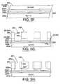
- FIG. 1is a plan layout view of a semiconductor wafer having a plurality of selective growth regions at spaced locations therein, according to an embodiment of the present invention.
- FIG. 2is a cross-section view of the wafer of FIG. 1 at a first intermediate stage of processing, taken along line 2 - 2 ′.
- FIG. 3is a plan layout view of a semiconductor wafer having a plurality of compound semiconductor layers thereon, according to an embodiment of the present invention.
- FIG. 4is a cross-sectional view of the wafer of FIG. 3 at a second intermediate stage of processing, taken along line 4 - 4 ′.
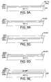
- FIGS. 5A-5Jare cross-sectional views of intermediate structures that illustrate a method of forming a single semiconductor layer of FIG. 4 using a pendeoepitaxial growth technique.
- FIGS. 1-4preferred methods of forming a plurality of compound semiconductor substrates will be described.
- FIGS. 1-2illustrate preferred steps of forming a plurality of selective growth regions 12 at spaced locations across a composite semiconductor substrate 10 .
- These selective growth regions 12may be rectangular in shape and have an area greater than about 1 ⁇ 10 4 ⁇ m 2 .
- the substrate 10may comprise a (111) silicon wafer having a plurality of semiconductor layers stacked thereon.
- the plurality of semiconductor layersmay include an underlying silicon carbide (SiC) layer, an intermediate aluminum nitride (AIN) layer on the silicon carbide layer and a gallium nitride (GaN) seed layer on the intermediate aluminum nitride layer, as described more fully hereinbelow with respect to FIGS. 5A-5J.
- Alternative exemplary substratesare also described in U.S. application Ser. No. 09/441,754, entitled “Methods of Fabricating Gallium Nitride Microelectronic Layers on Silicon Layers and Gallium Nitride Microelectronic Structures Formed Thereby”, filed Nov. 17, 1999, the disclosure of which is hereby incorporated herein by reference.
- Other substratesincluding those containing sapphire and/or compound semiconductor seed layers besides gallium nitride may also be used.
- each of the selective growth regions 12is preferably formed by selectively etching the substrate 10 to define a plurality of narrow parallel stripe-shaped trenches 14 and a plurality of parallel stripe-shaped semiconductor mesas 16 extending between the narrow trenches 14 .
- the depths of these trenches 14are preferably selected so that the sidewalls thereof expose portions of an underlying compound semiconductor seed layer.
- the semiconductor mesas 16may be formed to have a uniform width “W m ” and the narrow trenches 14 may formed to have a uniform width “W t ”. These widths may also be nonuniform.
- Typical values of W m and W tmay be about 1.0 ⁇ m and 4.0 ⁇ m, respectively.
- Each of the selective growth regions 12may also have a width “W sg ” and may be spaced from a next adjacent selective growth region 12 by a respective wide trench 18 having a width “W ds ”.
- Typical values for W sg and W dsmay be 500 ⁇ m and 50 ⁇ m, respectively.
- the value of W dsis also preferably set at a level greater than about ten (10) times W t .
- the narrow trenches 14 and wide trenches 18may be formed simultaneously by anisotropically etching the substrate 10 using a photolithographically patterned mask having openings therein where the trenches are to be formed.
- Typical etching techniquesinclude reactive ion etching (RI E) and inductively coupled plasma (ICP).
- Selective growth techniquesmay also be used to define the mesas 16 .
- pendeoepitaxial growth techniquesare preferably used to form a separate monocrystalline compound semiconductor layer 20 on each of the selective growth regions 12 .
- pendeoepitaxial growth techniquesmay be used to grow a respective monocrystalline gallium nitride layer from gallium nitride “seeds” that are exposed by the sidewalls of the mesas 16 within each selective growth region 12 .
- Exemplary pendeoepitaxial growth techniquesare more fully described in U.S. application Ser. No.
- 09/198,784entitled “Pendeoepitaxial Methods of Fabricating Gallium Nitride Semiconductor Layers on Silicon Carbide Substrates by Lateral Growth from Sidewalls of Masked Posts, and Gallium Nitride Semiconductor Structures Fabricated Thereby, filed Nov. 24, 1998, now U.S. Pat. No. 6,177,688, and in U.S. application Ser. No. 09/468,995, entitled “Pendeoepitaxial Methods of Fabricating Gallium Nitride Semiconductor Layers on Weak Posts, and Gallium Nitride Semiconductor Structures Fabricated Thereby, filed Dec. 21, 1999, the disclosures of which are hereby incorporated herein by reference.
- each selective growth region 12is separated from a next adjacent selective growth region 12 by a wide trench that preferably has a width at least about ten (10) times greater than the widths of the narrow trenches within a respective selective growth region 12
- adjacent monocrystalline compound semiconductor layers 20preferably do not coalesce with each other.
- each monocrystalline compound semiconductor layer 20is of sufficiently large dimension to ultimately serve as a separate compound semiconductor substrate or “platform” once the supporting substrate 10 has been diced along the dicing streets defined by each wide trench 18 , the failure of the adjacent compound semiconductor layers 20 to coalesce into a single wafer-sized layer need not limit the suitability of the preferred methods for large scale integrated circuit and optoelectronic applications.
- conventional techniquescan then be used to dice the substrate 10 into a plurality of separate compound semiconductor substrates.
- the wide trenches that extend between the grid of adjacent selective growth regionscan be treated as dicing streets for aligning the directional sawing of the substrate 10 in the x and y directions.
- the width of the wide trenchesis preferably selected so that the substrate 10 can be sawed without damaging the compound semiconductor layers 20 .
- the arrangement of each of the compound semiconductor layers 20may be designed to preserve usable active regions within the underlying substrate 10 .
- the arrangement of compound semiconductor layers 20may be designed so that after dicing each separate substrate (e.g., semiconductor chip) includes one or more compound semiconductor layers 20 thereon and one or more active regions therein in which semiconductor devices can be formed.
- each separate substratee.g., semiconductor chip
- the original substrate 10comprised a silicon carbide layer
- both gallium nitride and silicon carbide devicescould be integrated within a single semiconductor chip.
- a (111) silicon SIMOX supporting substrate 202is provided. As illustrated by FIG. 5A, this substrate 202 includes a buried layer of silicon dioxide 202 b therein that defines a (111) silicon surface layer 202 c on an underlying (111) silicon substrate 202 a .
- the buried layer of silicon dioxidemay be fabricated by implanting oxygen into a (111) silicon substrate to define a (111) silicon surface layer on the (111) silicon substrate.
- At least a portion of the (111) silicon surface layer 202 cis preferably converted to 3C-silicon carbide.
- a layer of 3C-silicon carbide 202 dis then epitaxially grown on the converted (111) silicon surface layer 202 c ′.
- the epitaxially grown layer of 3C-silicon carbide 202 doptionally is thinned to produce a thinned epitaxial layer of 3C-silicon carbide 202 d ′.
- a 2H-aluminum nitride layer and/or gallium nitride buffer layer 202 ethen is grown on the thinned epitaxially grown layer of 3C-silicon carbide 202 d ′, as illustrated by FIG. 5 E. Then, as shown by FIG. 5F, an underlying layer of 2H-gallium nitride 204 is grown on the buffer layer 202 e using, for example, a heteroepitaxial growth technique.
- FIGS. 5G-5Inow will show the use of pendeoepitaxy to laterally grow the underlying seed layer of 2H-gallium nitride 204 into a monocrystalline gallium nitride semiconductor layer.
- pendeoepitaxial techniquesmay be used advantageously to grow a monocrystalline gallium nitride semiconductor layer having an average defect density level therein of less than about 10 5 cm ⁇ 3 .
- the underlying gallium nitride layer 204may be formed to have a plurality of sidewalls 205 therein.
- the sidewalls 205may be thought of as being defined by a plurality of spaced apart posts 206 , that also may be referred to as “mesas”, “pedestals” or “columns”.
- the sidewalls 205also may be thought of as being defined by a plurality of trenches 207 , also referred to as “wells” in the underlying gallium nitride layer 204 .
- the sidewalls 205may also be thought of as being defined by a series of alternating trenches 207 and posts 206 .
- the posts 206 and the trenches 207 that define the sidewalls 205may be fabricated by selective etching, selective epitaxial growth and/or other conventional techniques. Moreover, it also will be understood that the sidewalls need not be orthogonal to the substrate 202 , but rather may be oblique thereto. Finally, it also will be understood that although the sidewalls 205 are shown in cross-section in FIG. 5G, the posts 206 and trenches 207 may define elongated regions that are straight, V-shaped or have other shapes.
- the trenches 207may also extend into the buffer layer 202 e and into the underlying silicon carbide layer 202 c ′/ 202 d ′, so that subsequent gallium nitride growth occurs preferentially on the sidewalls 205 rather than on the trench floors.
- the trenchesmay not extend into the silicon carbide layer 202 c ′/ 202 d ′, and also may not extend into buffer layer 202 e , depending, for example, on the trench geometry and the lateral versus vertical growth rates of the gallium nitride seed layer.
- the sidewalls 205 of the underlying gallium nitride layer 204are laterally grown to form a lateral gallium nitride layer 208 a in the trenches 207 .
- Lateral growth of gallium nitridemay be obtained at 1000-1100° C. and 45 Torr.
- the precursors TEG at 13-39 ⁇ mol/min and NH 3 at 1500 sccmmay be used in combination with a 3000 sccm H 2 diluent. If gallium nitride alloys are formed, additional conventional precursors of aluminum or indium, for example, may also be used.
- lateralmeans a direction that is orthogonal to the sidewalls 205 . It will also be understood that some vertical growth on the posts 206 may also take place during the lateral growth from sidewalls 205 . As used herein, the term “vertical” denotes a directional parallel to the sidewalls 205 .
- continued growth of the lateral gallium nitride layer 208 acauses vertical growth onto the underlying gallium nitride layer 204 , specifically onto the posts 206 , to form a vertical gallium nitride layer 208 b .
- Growth conditions for vertical growthmay be maintained as was described in connection with FIG. 5 H.
- continued vertical growth into trenches 207may take place at the bottom of the trenches.
- growthis allowed to continue until the lateral growth fronts coalesce in the trenches 207 at the interfaces 208 c , to form a continuous gallium nitride semiconductor layer in the trenches.
- the total growth timemay be approximately 60 minutes.
- each of the steps described above with respect to FIGS. 5A-5Jmay be performed simultaneously with respect to each of the selective growth regions 12 so that a plurality of compound semiconductor substrates 20 can be formed at spaced locations across a substrate 10 .
Landscapes
- Engineering & Computer Science (AREA)
- Physics & Mathematics (AREA)
- Condensed Matter Physics & Semiconductors (AREA)
- General Physics & Mathematics (AREA)
- Manufacturing & Machinery (AREA)
- Computer Hardware Design (AREA)
- Microelectronics & Electronic Packaging (AREA)
- Power Engineering (AREA)
- Chemical & Material Sciences (AREA)
- Materials Engineering (AREA)
- Led Devices (AREA)
- Junction Field-Effect Transistors (AREA)
Abstract
Description
This invention was made with Government support under Office of Naval Research Contract No. N00014-98-1-0384. The Government may have certain rights to this invention.
The present invention relates to methods of forming semiconductor substrates and substrates formed thereby, and more particularly to methods of forming compound semiconductor substrates and compound semiconductor substrates formed thereby.
Compound semiconductor materials such as gallium nitride (GaN) have been widely investigated as suitable substrate materials for microelectronic devices including but not limited to transistors, field emitters and optoelectronic devices. It will be understood that, as used herein, compound semiconductor materials may include III-V and II-VI alloys, for example. Reference to specific compound semiconductors such as gallium nitride will also be understood to include a family of gallium nitride alloys such as aluminum gallium nitride, indium gallium nitride and aluminum indium gallium nitride.
A major problem in fabricating gallium nitride-based microelectronic devices is the fabrication of gallium nitride semiconductor layers having low defect densities. It is known that one contributor to defect density is lattice mismatch with the substrate on which the gallium nitride layer is grown. Thus, although gallium nitride layers have been grown on sapphire substrates, it is known to reduce defect density by growing gallium nitride layers on aluminum nitride buffer layers which are themselves formed on silicon carbide substrates. Notwithstanding these advances, continued reduction in defect density is desirable.
It also is known to produce low defect density gallium nitride layers by forming a mask on a layer of gallium nitride, the mask including at least one opening that exposes the underlying layer of gallium nitride, and laterally growing the underlying layer of gallium nitride through the at least one opening and onto the mask. This technique often is referred to as “Epitaxial Lateral Overgrowth” (ELO). The layer of gallium nitride may be laterally grown until the gallium nitride coalesces on the mask to form a single layer on the mask. In order to form a continuous layer of gallium nitride with relatively low defect density, a second mask may be formed on the laterally overgrown gallium nitride layer, that includes at least one opening that is offset from the underlying mask. ELO then again is performed through the openings in the second mask to thereby overgrow a second low defect density continuous gallium nitride layer. Microelectronic devices then may be formed in this second overgrown layer. ELO of gallium nitride is described, for example, in the publications entitled Lateral Epitaxy of Low Defect Density GaN Layers Via Organometallic Vapor Phase Epitaxy to Nam et al., Appl. Phys. Lett. Vol. 71, No. 18, Nov. 3, 1997, pp. 2638-2640; and Dislocation Density Reduction Via Lateral Epitaxy in Selectively Grown GaN Structures to Zheleva et al, Appl. Phys.
Lett., Vol. 71, No. 17, Oct. 27, 1997, pp.2472-2474, the disclosures of which are hereby incorporated herein by reference.
It also is known to produce a layer of gallium nitride with low defect density by forming at least one trench or post in an underlying layer of gallium nitride to define at least one sidewall therein. A layer of gallium nitride is then laterally grown from the at least one sidewall which acts as a “seed”. Lateral growth preferably takes place until the laterally grown layers coalesce within the trenches. Lateral growth also preferably continues until the gallium nitride layer that is grown from the sidewalls laterally overgrows onto the tops of the posts. In order to facilitate lateral growth and produce nucleation of gallium nitride and growth in the vertical direction, the top of the posts and/or the trench floors may be masked.
Lateral growth from the sidewalls of trenches and/or posts also is referred to as “pendeoepitaxy” and is described, for example, in publications by Zheleva et al, entitled “Pendeo-Epitaxy: A New Approach for Lateral Growth of Gallium Nitride Films”, Journal of Electronic Materials, Vol. 28, No. 4, pp. L5-L8, February (1999) and Linthicum et al, entitled “Pendeoepitaxy of Gallium Nitride Thin Films” Applied Physics Letters, Vol. 75, No. 2, pp. 196-198, July (1999), the disclosures of which are hereby incorporated herein by reference. Pendeoepitaxy has also been shown to be successful at reducing threading dislocations and cracks caused by lattice mismatch by about three to four orders of magnitude relative to other conventional heteroepitaxy techniques. Nonetheless, because pendeoepitaxy may not always be successful in preventing the formation of cracks and bowing when large compound semiconductor layers such as gallium nitride are cooled to room temperature during back-end processing steps, there continues to be a need for improved methods of forming compound semiconductor layers with reduced susceptibility to cracking and bowing.
It is therefore an object of the present invention to provide improved methods of forming compound semiconductor substrates and substrates formed thereby.
It is another object of the present invention to provide methods of forming compound semiconductor substrates that can be less susceptible to cracking and bowing during back-end processing steps.
These and other objects, advantages and features of the present invention may be provided by methods of forming semiconductor substrates which include the steps of forming a plurality of selective growth regions at spaced locations on a first substrate and then forming a plurality of semiconductor layers at spaced locations on the first substrate by growing a respective semiconductor layer on each of the selective growth regions. The first substrate is then divided into a plurality of second smaller substrates that contain only a respective one of the plurality of semiconductor layers. This dividing step is preferably performed by partitioning (e.g., dicing) the first substrate at the spaces between the selective growth regions. Because this step of dividing the first substrate need not take place until all microelectronic processing steps have taken place, the first substrate with the selective growth regions may be processed on a wafer scale, as with conventional semiconductor wafers.
According to one preferred embodiment of the present invention, the step of forming a plurality of semiconductor layers preferably comprises growing a respective compound semiconductor layer (e.g., gallium nitride layer) on each of the selective growth regions. In particular, the growing step may comprise pendeoepitaxially growing a respective gallium nitride layer on each of the selective growth regions. Each of the selective growth regions is also preferably formed as a respective plurality of trenches that have sidewalls which expose compound semiconductor seeds from which epitaxial growth can take place. In particular, the step of forming a plurality of semiconductor layers may comprises epitaxially growing a first continuous semiconductor layer from sidewalls of a first plurality of trenches (within a first selective growth region) and epitaxially growing a second continuous semiconductor layer from sidewalls of a second plurality of trenches (within a second selective growth region). According to a preferred aspect of this embodiment of the present invention, when the growth steps are completed, the first continuous semiconductor layer and the second continuous semiconductor layer will have opposing edges that are spaced from each other by a wide trench that extends between adjacent edges of the first selective growth region and the second selective growth region.
Advantageously, because each selective growth region is separated from a next adjacent selective growth region by a wide trench the preferably has a width at least about ten (10) times greater than the widths of the narrower trenches within a respective selective growth region, adjacent monocrystalline compound semiconductor layers preferably do not coalesce with each other. Nonetheless, because each monocrystalline compound semiconductor layer is of sufficiently large dimension to ultimately serve as a separate compound semiconductor substrate or “platform” once the supporting substrate has been diced along the dicing streets defined by each wide trench, the failure of the adjacent compound semiconductor layers to coalesce into a single wafer-sized layer need not limit the suitability of the preferred methods for large scale integrated circuit and optoelectronic applications. Instead, by preventing adjacent compound semiconductor layers from coalescing with each other, the likelihood that the compound semiconductor layers will bow or crack upon cooling, as a result of lattice mismatch and thermal expansion coefficient differences, is substantially reduced. In other words, by growing separate compound semiconductor “platforms” separated by wide trenches, the lattice stress and concomitant build-up in strain within each “platform”, caused by differences in the thermal expansion coefficients of the compound semiconductor material and underlying substrate is greatly reduced relative to a large fully coalesced pendeoepitaxially formed compound semiconductor layer.
FIG. 1 is a plan layout view of a semiconductor wafer having a plurality of selective growth regions at spaced locations therein, according to an embodiment of the present invention.
FIG. 2 is a cross-section view of the wafer of FIG. 1 at a first intermediate stage of processing, taken along line2-2′.
FIG. 3 is a plan layout view of a semiconductor wafer having a plurality of compound semiconductor layers thereon, according to an embodiment of the present invention.
FIG. 4 is a cross-sectional view of the wafer of FIG. 3 at a second intermediate stage of processing, taken along line4-4′.
FIGS. 5A-5J are cross-sectional views of intermediate structures that illustrate a method of forming a single semiconductor layer of FIG. 4 using a pendeoepitaxial growth technique.
The present invention now will be described more fully hereinafter with reference to the accompanying drawings, in which preferred embodiments of the invention are shown. This invention may, however, be embodied in many different forms and should not be construed as limited to the embodiments set forth herein; rather, these embodiments are provided so that this disclosure will be thorough and complete, and will fully convey the scope of the invention to those skilled in the art. In the drawings, the thickness of layers and regions are exaggerated for clarity. Like numbers refer to like elements throughout. It will be understood that when an element such as a layer, region or substrate is referred to as being “on” another element, it can be directly on the other element or intervening elements may also be present. In contrast, when an element is referred to as being “directly on” another element, there are no intervening elements present.
Referring now to FIGS. 1-4, preferred methods of forming a plurality of compound semiconductor substrates will be described. In particular, FIGS. 1-2 illustrate preferred steps of forming a plurality ofselective growth regions 12 at spaced locations across acomposite semiconductor substrate 10. Theseselective growth regions 12 may be rectangular in shape and have an area greater than about 1×104μm2. According to one aspect of the present invention, thesubstrate 10 may comprise a (111) silicon wafer having a plurality of semiconductor layers stacked thereon. In particular, the plurality of semiconductor layers may include an underlying silicon carbide (SiC) layer, an intermediate aluminum nitride (AIN) layer on the silicon carbide layer and a gallium nitride (GaN) seed layer on the intermediate aluminum nitride layer, as described more fully hereinbelow with respect to FIGS. 5A-5J. Alternative exemplary substrates are also described in U.S. application Ser. No. 09/441,754, entitled “Methods of Fabricating Gallium Nitride Microelectronic Layers on Silicon Layers and Gallium Nitride Microelectronic Structures Formed Thereby”, filed Nov. 17, 1999, the disclosure of which is hereby incorporated herein by reference. Other substrates including those containing sapphire and/or compound semiconductor seed layers besides gallium nitride may also be used.
Referring now to FIG. 2, each of theselective growth regions 12 is preferably formed by selectively etching thesubstrate 10 to define a plurality of narrow parallel stripe-shapedtrenches 14 and a plurality of parallel stripe-shapedsemiconductor mesas 16 extending between thenarrow trenches 14. The depths of thesetrenches 14 are preferably selected so that the sidewalls thereof expose portions of an underlying compound semiconductor seed layer. As illustrated, thesemiconductor mesas 16 may be formed to have a uniform width “Wm” and thenarrow trenches 14 may formed to have a uniform width “Wt”. These widths may also be nonuniform. Typical values of Wmand Wtmay be about 1.0 μm and 4.0 μm, respectively. Each of theselective growth regions 12 may also have a width “Wsg” and may be spaced from a next adjacentselective growth region 12 by a respectivewide trench 18 having a width “Wds”. Typical values for Wsgand Wdsmay be 500 μm and 50 μm, respectively. The value of Wdsis also preferably set at a level greater than about ten (10) times Wt. As will be understood by those skilled in the art, thenarrow trenches 14 andwide trenches 18 may be formed simultaneously by anisotropically etching thesubstrate 10 using a photolithographically patterned mask having openings therein where the trenches are to be formed. Typical etching techniques include reactive ion etching (RI E) and inductively coupled plasma (ICP). Selective growth techniques may also be used to define themesas 16.
Referring now specifically to FIGS. 3-4, pendeoepitaxial growth techniques are preferably used to form a separate monocrystallinecompound semiconductor layer 20 on each of theselective growth regions 12. In particular, pendeoepitaxial growth techniques may be used to grow a respective monocrystalline gallium nitride layer from gallium nitride “seeds” that are exposed by the sidewalls of themesas 16 within eachselective growth region 12. Exemplary pendeoepitaxial growth techniques are more fully described in U.S. application Ser. No. 09/198,784, entitled “Pendeoepitaxial Methods of Fabricating Gallium Nitride Semiconductor Layers on Silicon Carbide Substrates by Lateral Growth from Sidewalls of Masked Posts, and Gallium Nitride Semiconductor Structures Fabricated Thereby, filed Nov. 24, 1998, now U.S. Pat. No. 6,177,688, and in U.S. application Ser. No. 09/468,995, entitled “Pendeoepitaxial Methods of Fabricating Gallium Nitride Semiconductor Layers on Weak Posts, and Gallium Nitride Semiconductor Structures Fabricated Thereby, filed Dec. 21, 1999, the disclosures of which are hereby incorporated herein by reference.
Advantageously, because eachselective growth region 12 is separated from a next adjacentselective growth region 12 by a wide trench that preferably has a width at least about ten (10) times greater than the widths of the narrow trenches within a respectiveselective growth region 12, adjacent monocrystalline compound semiconductor layers20 preferably do not coalesce with each other. However, because each monocrystallinecompound semiconductor layer 20 is of sufficiently large dimension to ultimately serve as a separate compound semiconductor substrate or “platform” once the supportingsubstrate 10 has been diced along the dicing streets defined by eachwide trench 18, the failure of the adjacent compound semiconductor layers20 to coalesce into a single wafer-sized layer need not limit the suitability of the preferred methods for large scale integrated circuit and optoelectronic applications. Instead, by preventingadjacent compound semiconductors 20 from coalescing with each other, the likelihood that the compound semiconductor layers20 will bow or crack upon cooling, as a result of lattice mismatch and thermal expansion coefficient differences, is substantially reduced. In other words, by growing separate compound semiconductor “platforms” separated by wide trenches, the lattice stress and concomitant build-up in strain within each “platform” caused by differences in the thermal expansion coefficients of the compound semiconductor material and underlying substrate is greatly reduced relative to a large fully coalesced pendeoepitaxially formed compound semiconductor layer.
Referring again to FIG. 3, conventional techniques can then be used to dice thesubstrate 10 into a plurality of separate compound semiconductor substrates. Here, the wide trenches that extend between the grid of adjacent selective growth regions can be treated as dicing streets for aligning the directional sawing of thesubstrate 10 in the x and y directions. The width of the wide trenches is preferably selected so that thesubstrate 10 can be sawed without damaging the compound semiconductor layers20. According to another aspect of the present invention, the arrangement of each of the compound semiconductor layers20 may be designed to preserve usable active regions within the underlyingsubstrate 10. For example, the arrangement of compound semiconductor layers20 may be designed so that after dicing each separate substrate (e.g., semiconductor chip) includes one or more compound semiconductor layers20 thereon and one or more active regions therein in which semiconductor devices can be formed. Thus, if eachcompound semiconductor layer 20 comprised gallium nitride and theoriginal substrate 10 comprised a silicon carbide layer, both gallium nitride and silicon carbide devices could be integrated within a single semiconductor chip.
Referring now to FIGS. 5A-5J, an exemplary method of forming a respective gallium nitride semiconductor layer on a central portion of aselective growth region 12 will be described. According to this exemplary method, a (111) siliconSIMOX supporting substrate 202 is provided. As illustrated by FIG. 5A, thissubstrate 202 includes a buried layer ofsilicon dioxide 202btherein that defines a (111)silicon surface layer 202con an underlying (111)silicon substrate 202a. The buried layer of silicon dioxide may be fabricated by implanting oxygen into a (111) silicon substrate to define a (111) silicon surface layer on the (111) silicon substrate. This process generally is referred to as SIMOX and is described for example in an article by Chen, entitled “Silicon-on-Insulator Why, How, and When”, AIP Conference Proceedings, Vol. 167, No. 1, pp. 310-319, Sep. 15, (1988).
Then, referring to FIG. 5B, at least a portion of the (111)silicon surface layer 202cis preferably converted to 3C-silicon carbide. As illustrated by FIG. 5C, a layer of 3C-silicon carbide 202dis then epitaxially grown on the converted (111)silicon surface layer 202c′. As shown in FIG. 5D, the epitaxially grown layer of 3C-silicon carbide 202doptionally is thinned to produce a thinned epitaxial layer of 3C-silicon carbide 202d′. A 2H-aluminum nitride layer and/or galliumnitride buffer layer 202ethen is grown on the thinned epitaxially grown layer of 3C-silicon carbide 202d′, as illustrated by FIG.5E. Then, as shown by FIG. 5F, an underlying layer of 2H-gallium nitride 204 is grown on thebuffer layer 202eusing, for example, a heteroepitaxial growth technique.
FIGS. 5G-5I now will show the use of pendeoepitaxy to laterally grow the underlying seed layer of 2H-gallium nitride 204 into a monocrystalline gallium nitride semiconductor layer. As described in the aforementioned U.S. application Ser. No. 09/441,754, pendeoepitaxial techniques may be used advantageously to grow a monocrystalline gallium nitride semiconductor layer having an average defect density level therein of less than about 105cm−3. Referring to FIG. 5G, the underlyinggallium nitride layer 204 may be formed to have a plurality ofsidewalls 205 therein. It will be understood by those having skill in the art that thesidewalls 205 may be thought of as being defined by a plurality of spaced apart posts206, that also may be referred to as “mesas”, “pedestals” or “columns”. Thesidewalls 205 also may be thought of as being defined by a plurality oftrenches 207, also referred to as “wells” in the underlyinggallium nitride layer 204. Thesidewalls 205 may also be thought of as being defined by a series of alternatingtrenches 207 and posts206. It will be understood that theposts 206 and thetrenches 207 that define thesidewalls 205 may be fabricated by selective etching, selective epitaxial growth and/or other conventional techniques. Moreover, it also will be understood that the sidewalls need not be orthogonal to thesubstrate 202, but rather may be oblique thereto. Finally, it also will be understood that although thesidewalls 205 are shown in cross-section in FIG. 5G, theposts 206 andtrenches 207 may define elongated regions that are straight, V-shaped or have other shapes. Thetrenches 207 may also extend into thebuffer layer 202eand into the underlyingsilicon carbide layer 202c′/202d′, so that subsequent gallium nitride growth occurs preferentially on thesidewalls 205 rather than on the trench floors. In other embodiments, the trenches may not extend into thesilicon carbide layer 202c′/202d′, and also may not extend intobuffer layer 202e, depending, for example, on the trench geometry and the lateral versus vertical growth rates of the gallium nitride seed layer.
Referring now to FIG. 5H, thesidewalls 205 of the underlyinggallium nitride layer 204 are laterally grown to form a lateralgallium nitride layer 208ain thetrenches 207. Lateral growth of gallium nitride may be obtained at 1000-1100° C. and 45 Torr. The precursors TEG at 13-39 μmol/min and NH3at 1500 sccm may be used in combination with a 3000 sccm H2diluent. If gallium nitride alloys are formed, additional conventional precursors of aluminum or indium, for example, may also be used. As used herein, the term “lateral” means a direction that is orthogonal to thesidewalls 205. It will also be understood that some vertical growth on theposts 206 may also take place during the lateral growth fromsidewalls 205. As used herein, the term “vertical” denotes a directional parallel to thesidewalls 205.
Referring now to FIG. 51, continued growth of the lateralgallium nitride layer 208acauses vertical growth onto the underlyinggallium nitride layer 204, specifically onto theposts 206, to form a verticalgallium nitride layer 208b. Growth conditions for vertical growth may be maintained as was described in connection with FIG.5H. As also shown in FIG. 5I, continued vertical growth intotrenches 207 may take place at the bottom of the trenches. Referring now to FIG. 5J, growth is allowed to continue until the lateral growth fronts coalesce in thetrenches 207 at theinterfaces 208c, to form a continuous gallium nitride semiconductor layer in the trenches. The total growth time may be approximately 60 minutes. As illustrated by FIG. 4, each of the steps described above with respect to FIGS. 5A-5J may be performed simultaneously with respect to each of theselective growth regions 12 so that a plurality ofcompound semiconductor substrates 20 can be formed at spaced locations across asubstrate 10.
In the drawings and specification, there have been disclosed typical preferred embodiments of the invention and, although specific terms are employed, they are used in a generic and descriptive sense only and not for purposes of limitation, the scope of the invention being set forth in the following claims.
Claims (36)
1. A method of forming a semiconductor substrate, comprising the steps of:
forming a plurality of selective growth regions at spaced locations on a first substrate, by forming a first selective growth region as a first plurality of trenches in the first substrate and forming a second selective growth region as a second plurality of trenches in the first substrate;
forming a plurality of semiconductor layers at spaced locations on the first substrate by epitaxially growing a first continuous semiconductor layer from sidewalls of the first plurality of trenches and epitaxially growing a second continuous semiconductor layer from sidewalls of the second plurality of trenches; and
dividing the first substrate into a plurality of second smaller substrates that contain only a respective one of the plurality of semiconductor layers, by partitioning the first substrate along a dicing trench that extends between the selective growth regions and is Wider than a width of each trench in the first plurality of trenches and a width of each trench in the second plurality of trenches.
2. The method of claim1, wherein said step of forming a plurality of semiconductor layers comprises epitaxially growing a first continuous semiconductor layer as a compound semiconductor layer.
3. The method of claim2, wherein the compound semiconductor layer comprises gallium nitride.
4. The method of claim2, wherein said step of epitaxially growing a first continuous semiconductor layer comprises pendeoepitaxially growing a gallium nitride layer from sidewalls of the first plurality of trenches.
5. The method of claim1, wherein the wide trench constitutes a dicing street; and wherein said dividing step comprises dicing the first substrate along the dicing street.
6. The method of claim5, wherein the wide trench is sufficiently wide to enable the first substrate to be diced without dicing the first and second continuous semiconductor layers.
7. The method of claim4, wherein the first substrate comprises a gallium nitride seed layer; and wherein said step of forming a first selective growth region comprises selectively etching the gallium nitride seed layer to define a first plurality of trenches therein.
8. The method of claim7, wherein said step of forming a plurality of semiconductor layers comprises pendeoepitaxially growing a first continuous gallium nitride layer from the gallium nitride seed layer.
9. A method of forming a semiconductor substrate, comprising the steps of:
forming a first selective growth region as a first plurality of trenches in a gallium nitride seed layer;
forming a second selective growth region as a second plurality of trenches in the gallium nitride seed layer;
pendeoepitaxially growing a first continuous gallium nitride layer from sidewalls of the first plurality of trenches;
pendeoepitaxially growing a second continuous gallium nitride layer from sidewalls of the second plurality of trenches; and
partitioning the gallium nitride seed layer between the first plurality of trenches and the second plurality of trenches, to define a first substrate comprising the first continuous gallium nitride layer and a second substrate comprising the second continuous gallium nitride layer.
10. The method of claim9, wherein the first continuous gallium nitride layer and the second continuous gallium nitride layer have opposing edges that are spaced from each other by a wide trench that extends between adjacent edges of the first selective growth region and the second selective growth region.
11. The method of claim10, wherein the wide trench constitutes a dicing street; and wherein said dividing step comprises dicing the first substrate along the dicing street.
12. The method of claim11, wherein the wide trench is sufficiently wide to enable the first substrate to be diced without dicing the first and second continuous gallium nitride layers.
13. A method of forming a plurality of gallium nitride substrates, comprising the steps of:
forming a plurality of trench arrays at spaced locations in a gallium nitride seed layer, each of said plurality of trench arrays spaced from another trench array by a respective dicing trench;
pendeoepitaxially growing a respective gallium nitride layer on each of the trench arrays; and
dividing the gallium nitride seed layer into a plurality of gallium nitride substrates by dicing the gallium nitride seed layer along a dicing street defined by a dicing trench.
14. The method of claim13, wherein the plurality of trench arrays are arranged as a two-dimensional grid of trench arrays.
15. The method of claim14, wherein said step of forming a plurality of trench arrays is preceded by the step of heteroepitaxially forming a gallium nitride seed layer on a substrate.
16. The method of claim13, wherein said step of forming a plurality of trench arrays is preceded by the step of heteroepitaxially forming a gallium nitride seed layer on a substrate.
17. The method of claim13, wherein said step of forming a plurality of trench arrays is preceded by the step of forming a gallium nitride seed layer on a substrate that comprises a material selected from the group consisting of silicon, silicon carbide and sapphire.
18. The method of claim13, wherein said step of pendeoepitaxially growing a respective gallium nitride layer comprises pendeoepitaxially growing on each of the trench arrays a respective gallium nitride layer having an average defect density of less than about 105cm−3therein.
19. The method of claim13, wherein each of the gallium nitride layers has a surface area greater than about 10,000 μm2.
20. A method of forming a plurality of compound semiconductor substrates, comprising the steps of:
forming a plurality of trench arrays at spaced locations in a compound semiconductor seed layer;
growing a respective compound semiconductor layer on each of the trench arrays; and
dividing the compound semiconductor seed layer into a plurality of compound semiconductor substrates by dicing the compound semiconductor seed layer along dicing streets extending between the plurality of trench arrays.
21. The method of claim20, wherein the plurality of trench arrays are arranged as a two-dimensional grid of trench arrays.
22. The method of claim20, wherein said step of forming a plurality of trench arrays is preceded by the step of heteroepitaxially forming a compound semiconductor seed layer on a substrate.
23. The method of claim22, wherein said step of forming a plurality of trench arrays is preceded by the step of forming a compound semiconductor seed layer on a substrate that comprises a material selected from the group consisting of silicon, silicon carbide and sapphire.
24. The method claim20, wherein said step of growing a respective compound semiconductor layer comprises pendeoepitaxially growing a respective compound semiconductor layer on each of the plurality of trench arrays.
25. The method claim23, wherein said step of forming a plurality of trench arrays comprises selectively etching the compound semiconductor seed layer to define a plurality of trenches having sidewalls that expose the compound semiconductor seed layer and the substrate.
26. The method claim25, wherein said step of growing a respective compound semiconductor layer comprises pendeoepitaxially growing a monocrystalline compound semiconductor layer from the exposed compound semiconductor seed layer.
27. A method of forming a semiconductor substrate, comprising the steps of:
forming first and second semiconductor growth regions that are spaced apart by a dicing trench, on a supporting substrate comprising a semiconductor seed layer, said first semiconductor growth region comprising a first plurality of trenches that extend into the semiconductor seed layer,
simultaneously epitaxially growing first and second continuous semiconductor layers that are spaced apart from each other but overhang a bottom of the dicing trench, from the first and second semiconductor growth regions, respectively, and without forming an epitaxial growth mask in the dicing trench; and
forming first and second semiconductor substrates comprising the first and second continuous semiconductor layers, respectively, by dicing the supporting substrate along the dicing trench.
28. The method of claim27, wherein said step of simultaneously epitaxially growing first and second continuous semiconductor layers comprises pendeoepitaxially growing the first continuous semiconductor layer from sidewalls of the first plurality of trenches.
29. The method of claim28, wherein the first continuous semiconductor layer comprises gallium nitride.
30. The method of claim27, wherein a width of the dicing trench is greater than about ten times a width of a trench in the first plurality of trenches.
31. A method of forming a semiconductor substrate, comprising the steps of:
forming a plurality of selective growth regions at spaced locations on a first substrate, by forming a first selective growth region as a first plurality of trenches in the first substrate and forming a second selective growth region as a second plurality of trenches in the first substrate;
forming a plurality of semiconductor layers at spaced locations on the first substrate by growing a first continuous semiconductor layer from at least portions of first mesas defined by the first plurality of trenches and growing a second continuous semiconductor layer from at least portions of second mesas defined by the second plurality of trenches; and
dividing the first substrate into a plurality of second smaller substrates that contain only a respective one of the plurality of semiconductor layers, by partitioning the first substrate between the selective growth regions.
32. The method of claim31, wherein said step of forming a plurality of semiconductor layers comprises epitaxially growing a first continuous semiconductor layer as a compound semiconductor layer.
33. The method of claim32, wherein the compound semiconductor layer comprises gallium nitride.
34. The method of claim32, wherein said step of epitaxially growing a first continuous semiconductor layer comprises pendeoepitaxially growing a gallium nitride layer from sidewalls of the first plurality of trenches.
35. The method of claim31, wherein the portions of first mesas defined by the first plurality of trenches comprise top surfaces of the first mesas.
36. The method of claim33, wherein the portions of first mesas defined by the first plurality of trenches comprise top surfaces of the first mesas.
Priority Applications (4)
| Application Number | Priority Date | Filing Date | Title |
|---|---|---|---|
| US09/512,242US6261929B1 (en) | 2000-02-24 | 2000-02-24 | Methods of forming a plurality of semiconductor layers using spaced trench arrays |
| PCT/US2001/005249WO2001063654A2 (en) | 2000-02-24 | 2001-02-20 | Methods of forming a plurality of semiconductor layers using trench arrays |
| AU2001243186AAU2001243186A1 (en) | 2000-02-24 | 2001-02-20 | Methods of forming a plurality of semiconductor layers using spaced trench arrays and semiconductor substrates formed thereby |
| US09/906,258US6486042B2 (en) | 2000-02-24 | 2001-07-16 | Methods of forming compound semiconductor layers using spaced trench arrays and semiconductor substrates formed thereby |
Applications Claiming Priority (1)
| Application Number | Priority Date | Filing Date | Title |
|---|---|---|---|
| US09/512,242US6261929B1 (en) | 2000-02-24 | 2000-02-24 | Methods of forming a plurality of semiconductor layers using spaced trench arrays |
Related Child Applications (1)
| Application Number | Title | Priority Date | Filing Date |
|---|---|---|---|
| US09/906,258ContinuationUS6486042B2 (en) | 2000-02-24 | 2001-07-16 | Methods of forming compound semiconductor layers using spaced trench arrays and semiconductor substrates formed thereby |
Publications (1)
| Publication Number | Publication Date |
|---|---|
| US6261929B1true US6261929B1 (en) | 2001-07-17 |
Family
ID=24038275
Family Applications (2)
| Application Number | Title | Priority Date | Filing Date |
|---|---|---|---|
| US09/512,242Expired - LifetimeUS6261929B1 (en) | 2000-02-24 | 2000-02-24 | Methods of forming a plurality of semiconductor layers using spaced trench arrays |
| US09/906,258Expired - LifetimeUS6486042B2 (en) | 2000-02-24 | 2001-07-16 | Methods of forming compound semiconductor layers using spaced trench arrays and semiconductor substrates formed thereby |
Family Applications After (1)
| Application Number | Title | Priority Date | Filing Date |
|---|---|---|---|
| US09/906,258Expired - LifetimeUS6486042B2 (en) | 2000-02-24 | 2001-07-16 | Methods of forming compound semiconductor layers using spaced trench arrays and semiconductor substrates formed thereby |
Country Status (3)
| Country | Link |
|---|---|
| US (2) | US6261929B1 (en) |
| AU (1) | AU2001243186A1 (en) |
| WO (1) | WO2001063654A2 (en) |
Cited By (132)
| Publication number | Priority date | Publication date | Assignee | Title |
|---|---|---|---|---|
| US6462355B1 (en) | 1998-11-24 | 2002-10-08 | North Carolina State University | Pendeoepitaxial gallium nitride semiconductor layers on silicon carbide substrates |
| US6486042B2 (en)* | 2000-02-24 | 2002-11-26 | North Carolina State University | Methods of forming compound semiconductor layers using spaced trench arrays and semiconductor substrates formed thereby |
| US6489221B2 (en)* | 1999-11-17 | 2002-12-03 | North Carolina State University | High temperature pendeoepitaxial methods of fabricating gallium nitride semiconductor layers on sapphire substrates |
| US6518079B2 (en)* | 2000-12-20 | 2003-02-11 | Lumileds Lighting, U.S., Llc | Separation method for gallium nitride devices on lattice-mismatched substrates |
| US20030034529A1 (en)* | 2000-12-04 | 2003-02-20 | Amberwave Systems Corporation | CMOS inverter and integrated circuits utilizing strained silicon surface channel MOSFETs |
| US20030042555A1 (en)* | 2001-08-30 | 2003-03-06 | Shindengen Electric Manufacturing Co., Ltd. | Transistor and diode |
| DE10142656A1 (en)* | 2001-08-31 | 2003-03-27 | Osram Opto Semiconductors Gmbh | Production of a III-V nitride semiconductor layer based on gallium nitride comprises applying a mask layer on a substrate to form masked regions and non-masked regions, and growing nitride semiconductor layer over the non-masked regions |
| US20030066816A1 (en)* | 2001-09-17 | 2003-04-10 | Schultz Gary A. | Uniform patterning for deep reactive ion etching |
| US20030080345A1 (en)* | 2001-09-19 | 2003-05-01 | Sumitomo Electric Industries, Ltd. | Single crystal GaN substrate, method of growing same and method of producing same |
| US6573126B2 (en) | 2000-08-16 | 2003-06-03 | Massachusetts Institute Of Technology | Process for producing semiconductor article using graded epitaxial growth |
| US20030102498A1 (en)* | 2001-09-24 | 2003-06-05 | Glyn Braithwaite | RF circuits including transistors having strained material layers |
| US6599361B2 (en)* | 2001-06-18 | 2003-07-29 | National Research Council Of Canada | GaN selective growth on SiC substrates by ammonia-source MBE |
| US6602613B1 (en)* | 2000-01-20 | 2003-08-05 | Amberwave Systems Corporation | Heterointegration of materials using deposition and bonding |
| US6611002B2 (en) | 2001-02-23 | 2003-08-26 | Nitronex Corporation | Gallium nitride material devices and methods including backside vias |
| US20030160232A1 (en)* | 2000-06-19 | 2003-08-28 | Nichia Corporation | Nitride semiconductor substrate and method for manufacturing the same, and nitride semiconductor device using nitride semiconductor substrate |
| US6617060B2 (en) | 2000-12-14 | 2003-09-09 | Nitronex Corporation | Gallium nitride materials and methods |
| US6617261B2 (en)* | 2001-12-18 | 2003-09-09 | Xerox Corporation | Structure and method for fabricating GaN substrates from trench patterned GaN layers on sapphire substrates |
| US6649480B2 (en) | 2000-12-04 | 2003-11-18 | Amberwave Systems Corporation | Method of fabricating CMOS inverter and integrated circuits utilizing strained silicon surface channel MOSFETs |
| DE10218498A1 (en)* | 2002-04-25 | 2003-11-20 | Osram Opto Semiconductors Gmbh | Production of a semiconductor layer comprises preparing a substrate, applying a mask layer having openings on the substrate, and growing a semiconductor layer |
| US20040000268A1 (en)* | 1998-04-10 | 2004-01-01 | Massachusetts Institute Of Technology | Etch stop layer system |
| US20040043584A1 (en)* | 2002-08-27 | 2004-03-04 | Thomas Shawn G. | Semiconductor device and method of making same |
| US6703688B1 (en) | 2001-03-02 | 2004-03-09 | Amberwave Systems Corporation | Relaxed silicon germanium platform for high speed CMOS electronics and high speed analog circuits |
| US20040069212A1 (en)* | 2002-10-10 | 2004-04-15 | Neudeck Philip G. | Lateral movement of screw dislocations during homoepitaxial growth and devices yielded therefrom free of the detrimental effects of screw dislocations |
| US6723661B2 (en) | 2001-03-02 | 2004-04-20 | Amberwave Systems Corporation | Relaxed silicon germanium platform for high speed CMOS electronics and high speed analog circuits |
| US6724008B2 (en) | 2001-03-02 | 2004-04-20 | Amberwave Systems Corporation | Relaxed silicon germanium platform for high speed CMOS electronics and high speed analog circuits |
| US20040075105A1 (en)* | 2002-08-23 | 2004-04-22 | Amberwave Systems Corporation | Semiconductor heterostructures having reduced dislocation pile-ups and related methods |
| US20040087115A1 (en)* | 2001-03-22 | 2004-05-06 | Seiji Nagai | Production method of III nitride compound semiconductor, and III nitride compound semiconductor element based on it |
| US6750130B1 (en) | 2000-01-20 | 2004-06-15 | Amberwave Systems Corporation | Heterointegration of materials using deposition and bonding |
| US20040123796A1 (en)* | 2001-02-14 | 2004-07-01 | Seiji Nagai | Production method for semiconductor crystal and semiconductor luminous element |
| US20040130002A1 (en)* | 2001-02-23 | 2004-07-08 | Nitronex Corporation | Gallium nitride material devices and methods of forming the same |
| US20040169192A1 (en)* | 2001-06-04 | 2004-09-02 | Hisaki Kato | Method for producing group III nitride compounds semiconductor |
| US6818532B2 (en)* | 2002-04-09 | 2004-11-16 | Oriol, Inc. | Method of etching substrates |
| US20050009304A1 (en)* | 1998-06-10 | 2005-01-13 | Tsvetanka Zheleva | Methods of fabricating gallium nitride semiconductor layers by lateral growth into trenches |
| US6864115B2 (en) | 2000-01-20 | 2005-03-08 | Amberwave Systems Corporation | Low threading dislocation density relaxed mismatched epilayers without high temperature growth |
| US6876010B1 (en) | 1997-06-24 | 2005-04-05 | Massachusetts Institute Of Technology | Controlling threading dislocation densities in Ge on Si using graded GeSi layers and planarization |
| US20050127397A1 (en)* | 2001-02-23 | 2005-06-16 | Nitronex Corporation | Gallium nitride materials including thermally conductive regions |
| US20050133818A1 (en)* | 2003-12-17 | 2005-06-23 | Johnson Jerry W. | Gallium nitride material devices including an electrode-defining layer and methods of forming the same |
| US20050145851A1 (en)* | 2003-12-17 | 2005-07-07 | Nitronex Corporation | Gallium nitride material structures including isolation regions and methods |
| US20050167775A1 (en)* | 2003-08-05 | 2005-08-04 | Nitronex Corporation | Gallium nitride material transistors and methods associated with the same |
| US6940089B2 (en) | 2001-04-04 | 2005-09-06 | Massachusetts Institute Of Technology | Semiconductor device structure |
| US20050195012A1 (en)* | 2004-03-02 | 2005-09-08 | Atsushi Sueoka | Semiconductor device |
| US20050258450A1 (en)* | 2004-05-20 | 2005-11-24 | Saxler Adam W | Semiconductor devices having a hybrid channel layer, current aperture transistors and methods of fabricating same |
| US20050285155A1 (en)* | 2004-06-28 | 2005-12-29 | Nitronex Corporation | Semiconductor device-based sensors and methods associated with the same |
| US20050285142A1 (en)* | 2004-06-28 | 2005-12-29 | Nitronex Corporation | Gallium nitride materials and methods associated with the same |
| US20060006500A1 (en)* | 2004-07-07 | 2006-01-12 | Nitronex Corporation | III-nitride materials including low dislocation densities and methods associated with the same |
| US20060017064A1 (en)* | 2004-07-26 | 2006-01-26 | Saxler Adam W | Nitride-based transistors having laterally grown active region and methods of fabricating same |
| US6995430B2 (en) | 2002-06-07 | 2006-02-07 | Amberwave Systems Corporation | Strained-semiconductor-on-insulator device structures |
| US20060108606A1 (en)* | 2004-11-23 | 2006-05-25 | Saxler Adam W | Cap layers and/or passivation layers for nitride-based transistors, transistor structures and methods of fabricating same |
| US20060118809A1 (en)* | 2004-12-06 | 2006-06-08 | Primit Parikh | High power density and/or linearity transistors |
| US20060118823A1 (en)* | 2004-12-06 | 2006-06-08 | Primit Parikh | Field effect transistors (FETs) having multi-watt output power at millimeter-wave frequencies |
| US7060632B2 (en) | 2002-03-14 | 2006-06-13 | Amberwave Systems Corporation | Methods for fabricating strained layers on semiconductor substrates |
| US7074623B2 (en) | 2002-06-07 | 2006-07-11 | Amberwave Systems Corporation | Methods of forming strained-semiconductor-on-insulator finFET device structures |
| US20060208280A1 (en)* | 2005-03-15 | 2006-09-21 | Smith Richard P | Group III nitride field effect transistors (FETS) capable of withstanding high temperature reverse bias test conditions |
| US20060214289A1 (en)* | 2004-10-28 | 2006-09-28 | Nitronex Corporation | Gallium nitride material-based monolithic microwave integrated circuits |
| US20060226412A1 (en)* | 2005-04-11 | 2006-10-12 | Saxler Adam W | Thick semi-insulating or insulating epitaxial gallium nitride layers and devices incorporating same |
| US20060226413A1 (en)* | 2005-04-11 | 2006-10-12 | Saxler Adam W | Composite substrates of conductive and insulating or semi-insulating group III-nitrides for group III-nitride devices |
| US7122449B2 (en) | 2002-06-10 | 2006-10-17 | Amberwave Systems Corporation | Methods of fabricating semiconductor structures having epitaxially grown source and drain elements |
| US20060244011A1 (en)* | 2005-04-29 | 2006-11-02 | Saxler Adam W | Binary group III-nitride based high electron mobility transistors and methods of fabricating same |
| US20060244010A1 (en)* | 2005-04-29 | 2006-11-02 | Saxler Adam W | Aluminum free group III-nitride based high electron mobility transistors and methods of fabricating same |
| US20060249748A1 (en)* | 2005-05-03 | 2006-11-09 | Nitronex Corporation | Gallium nitride material structures including substrates and methods associated with the same |
| US20060270076A1 (en)* | 2005-05-31 | 2006-11-30 | The Regents Of The University Of California | Defect reduction of non-polar and semi-polar III-nitrides with sidewall lateral epitaxial overgrowth (SLEO) |
| US20060267043A1 (en)* | 2005-05-27 | 2006-11-30 | Emerson David T | Deep ultraviolet light emitting devices and methods of fabricating deep ultraviolet light emitting devices |
| US20070004184A1 (en)* | 2005-06-29 | 2007-01-04 | Saxler Adam W | Low dislocation density group III nitride layers on silicon carbide substrates and methods of making the same |
| US20070000433A1 (en)* | 2005-06-15 | 2007-01-04 | Mike Briere | III-nitride semiconductor device fabrication |
| US20070018198A1 (en)* | 2005-07-20 | 2007-01-25 | Brandes George R | High electron mobility electronic device structures comprising native substrates and methods for making the same |
| US7217603B2 (en) | 2002-06-25 | 2007-05-15 | Amberwave Systems Corporation | Methods of forming reacted conductive gate electrodes |
| US20070141823A1 (en)* | 2005-12-12 | 2007-06-21 | Kyma Technologies, Inc. | Inclusion-free uniform semi-insulating group III nitride substrates and methods for making same |
| US20070164315A1 (en)* | 2004-11-23 | 2007-07-19 | Cree, Inc. | Cap Layers Including Aluminum Nitride for Nitride-Based Transistors and Methods of Fabricating Same |
| US7247889B2 (en) | 2004-12-03 | 2007-07-24 | Nitronex Corporation | III-nitride material structures including silicon substrates |
| US20070190755A1 (en)* | 2006-02-16 | 2007-08-16 | Samsung Electronics Co., Ltd. | Substrate for growing Pendeo epitaxy and method of forming the same |
| US20070202360A1 (en)* | 2005-10-04 | 2007-08-30 | Nitronex Corporation | Gallium nitride material transistors and methods for wideband applications |
| US20070272957A1 (en)* | 2005-12-02 | 2007-11-29 | Nitronex Corporation | Gallium nitride material devices and associated methods |
| US7307273B2 (en) | 2002-06-07 | 2007-12-11 | Amberwave Systems Corporation | Control of strain in device layers by selective relaxation |
| US20080035143A1 (en)* | 2006-08-14 | 2008-02-14 | Sievers Robert E | Human-powered dry powder inhaler and dry powder inhaler compositions |
| US7332417B2 (en) | 2003-01-27 | 2008-02-19 | Amberwave Systems Corporation | Semiconductor structures with structural homogeneity |
| US7335545B2 (en) | 2002-06-07 | 2008-02-26 | Amberwave Systems Corporation | Control of strain in device layers by prevention of relaxation |
| US20080054292A1 (en)* | 2006-08-31 | 2008-03-06 | Industrial Technology Research Institute | Nitride semiconductor substrate, method for forming a nitride semiconductor layer and method for separating the nitride semiconductor layer from the substrate |
| US20080102610A1 (en)* | 2000-08-04 | 2008-05-01 | The Regents Of The University Of California | Method of controlling stress in gallium nitride films deposited on substrates |
| US7368756B2 (en) | 2002-07-19 | 2008-05-06 | Cree, Inc. | Trench cut light emitting diodes and methods of fabricating same |
| US7393733B2 (en) | 2004-12-01 | 2008-07-01 | Amberwave Systems Corporation | Methods of forming hybrid fin field-effect transistor structures |
| US20080163814A1 (en)* | 2006-12-12 | 2008-07-10 | The Regents Of The University Of California | CRYSTAL GROWTH OF M-PLANE AND SEMIPOLAR PLANES OF (Al, In, Ga, B)N ON VARIOUS SUBSTRATES |
| US20080197358A1 (en)* | 2007-02-19 | 2008-08-21 | Alcatel-Lucent | Wide-bandgap semiconductor devices |
| JP2008536319A (en)* | 2005-04-15 | 2008-09-04 | ラティス パワー (チアンシ) コーポレイション | Method for forming an InGaAlN film and a light emitting device on a silicon substrate |
| US7504704B2 (en) | 2003-03-07 | 2009-03-17 | Amberwave Systems Corporation | Shallow trench isolation process |
| US20090079034A1 (en)* | 2007-09-26 | 2009-03-26 | Wang Nang Wang | Non-polar iii-v nitride semiconductor and growth method |
| US20090140274A1 (en)* | 2007-12-04 | 2009-06-04 | Philips Lumileds Lighting Company, Llc | III-Nitride Light Emitting Device Including Porous Semiconductor Layer |
| US20090174038A1 (en)* | 2007-01-19 | 2009-07-09 | Wang Nang Wang | Production of single-crystal semiconductor material using a nanostructure template |
| US7566913B2 (en) | 2005-12-02 | 2009-07-28 | Nitronex Corporation | Gallium nitride material devices including conductive regions and methods associated with the same |
| US20090194773A1 (en)* | 2008-02-05 | 2009-08-06 | Nitronex Corporation | Gallium nitride material devices including diamond regions and methods associated with the same |
| US7592211B2 (en) | 2006-01-17 | 2009-09-22 | Cree, Inc. | Methods of fabricating transistors including supported gate electrodes |
| US7594967B2 (en) | 2002-08-30 | 2009-09-29 | Amberwave Systems Corporation | Reduction of dislocation pile-up formation during relaxed lattice-mismatched epitaxy |
| US20090243043A1 (en)* | 2006-03-23 | 2009-10-01 | Wang Nang Wang | Growth method using nanostructure compliant layers and hvpe for producing high quality compound semiconductor materials |
| US20090267188A1 (en)* | 2008-04-29 | 2009-10-29 | Nitronex Corporation | Gallium nitride material processing and related device structures |
| US7615829B2 (en) | 2002-06-07 | 2009-11-10 | Amberwave Systems Corporation | Elevated source and drain elements for strained-channel heterojuntion field-effect transistors |
| US7709269B2 (en) | 2006-01-17 | 2010-05-04 | Cree, Inc. | Methods of fabricating transistors including dielectrically-supported gate electrodes |
| US20100119845A1 (en)* | 2008-11-10 | 2010-05-13 | National Central University | Manufacturing method of nitride crystalline film, nitride film and substrate structure |
| US7745848B1 (en) | 2007-08-15 | 2010-06-29 | Nitronex Corporation | Gallium nitride material devices and thermal designs thereof |
| US7776697B2 (en) | 2001-09-21 | 2010-08-17 | Taiwan Semiconductor Manufacturing Company, Ltd. | Semiconductor structures employing strained material layers with defined impurity gradients and methods for fabricating same |
| US20110037098A1 (en)* | 2009-08-17 | 2011-02-17 | Samsung Electronics Co., Ltd. | Substrate structures and methods of manufacturing the same |
| US20120161158A1 (en)* | 2010-10-18 | 2012-06-28 | Sumitomo Electric Industries, Ltd. | Combined substrate having silicon carbide substrate |
| CN102696120A (en)* | 2010-01-15 | 2012-09-26 | 皇家飞利浦电子股份有限公司 | Method for forming composite substrate and growing III-V light-emitting device on composite substrate |
| US20120252191A1 (en)* | 2007-10-18 | 2012-10-04 | Rajaram Bhat | Gallium nitride semiconductor device on soi and process for making same |
| WO2012138821A3 (en)* | 2011-04-08 | 2014-05-01 | Lux Material Co., Ltd. | Reusable substrates for electronic device fabrication and methods thereof |
| US8748292B2 (en) | 2002-06-07 | 2014-06-10 | Taiwan Semiconductor Manufacturing Company, Ltd. | Methods of forming strained-semiconductor-on-insulator device structures |
| US8822282B2 (en) | 2001-03-02 | 2014-09-02 | Taiwan Semiconductor Manufacturing Company, Ltd. | Methods of fabricating contact regions for FET incorporating SiGe |
| US8956960B2 (en)* | 2012-11-16 | 2015-02-17 | Infineon Technologies Ag | Method for stress reduced manufacturing semiconductor devices |
| US20150053916A1 (en)* | 2013-08-22 | 2015-02-26 | Nanoco Technologies Ltd. | Gas Phase Enhancement of Emission Color Quality in Solid State LEDs |
| US9627473B2 (en) | 2015-09-08 | 2017-04-18 | Macom Technology Solutions Holdings, Inc. | Parasitic channel mitigation in III-nitride material semiconductor structures |
| US9673281B2 (en) | 2015-09-08 | 2017-06-06 | Macom Technology Solutions Holdings, Inc. | Parasitic channel mitigation using rare-earth oxide and/or rare-earth nitride diffusion barrier regions |
| US9704705B2 (en) | 2015-09-08 | 2017-07-11 | Macom Technology Solutions Holdings, Inc. | Parasitic channel mitigation via reaction with active species |
| US9752252B1 (en)* | 2009-01-21 | 2017-09-05 | Stc.Unm | Cubic phase, nitrogen-based compound semiconductor films |
| US9773898B2 (en) | 2015-09-08 | 2017-09-26 | Macom Technology Solutions Holdings, Inc. | III-nitride semiconductor structures comprising spatially patterned implanted species |
| US9799520B2 (en) | 2015-09-08 | 2017-10-24 | Macom Technology Solutions Holdings, Inc. | Parasitic channel mitigation via back side implantation |
| US9806182B2 (en) | 2015-09-08 | 2017-10-31 | Macom Technology Solutions Holdings, Inc. | Parasitic channel mitigation using elemental diboride diffusion barrier regions |
| EP3198649A4 (en)* | 2014-09-25 | 2018-05-16 | Intel Corporation | Iii-n epitaxial device structures on free standing silicon mesas |
| US10211294B2 (en) | 2015-09-08 | 2019-02-19 | Macom Technology Solutions Holdings, Inc. | III-nitride semiconductor structures comprising low atomic mass species |
| US10388777B2 (en) | 2015-06-26 | 2019-08-20 | Intel Corporation | Heteroepitaxial structures with high temperature stable substrate interface material |
| US10573647B2 (en) | 2014-11-18 | 2020-02-25 | Intel Corporation | CMOS circuits using n-channel and p-channel gallium nitride transistors |
| US10658471B2 (en) | 2015-12-24 | 2020-05-19 | Intel Corporation | Transition metal dichalcogenides (TMDCS) over III-nitride heteroepitaxial layers |
| US10665708B2 (en) | 2015-05-19 | 2020-05-26 | Intel Corporation | Semiconductor devices with raised doped crystalline structures |
| US10700023B2 (en) | 2016-05-18 | 2020-06-30 | Macom Technology Solutions Holdings, Inc. | High-power amplifier package |
| US10707308B2 (en) | 2017-12-24 | 2020-07-07 | HangZhou HaiCun Information Technology Co., Ltd. | Hetero-epitaxial output device array |
| US10756183B2 (en) | 2014-12-18 | 2020-08-25 | Intel Corporation | N-channel gallium nitride transistors |
| US10930500B2 (en) | 2014-09-18 | 2021-02-23 | Intel Corporation | Wurtzite heteroepitaxial structures with inclined sidewall facets for defect propagation control in silicon CMOS-compatible semiconductor devices |
| US11038023B2 (en) | 2018-07-19 | 2021-06-15 | Macom Technology Solutions Holdings, Inc. | III-nitride material semiconductor structures on conductive silicon substrates |
| US11233053B2 (en) | 2017-09-29 | 2022-01-25 | Intel Corporation | Group III-nitride (III-N) devices with reduced contact resistance and their methods of fabrication |
| US11264465B2 (en) | 2015-09-08 | 2022-03-01 | Macom Technology Solutions Holdings, Inc. | Parasitic channel mitigation using silicon carbide diffusion barrier regions |
| CN114258591A (en)* | 2019-06-21 | 2022-03-29 | 原子能与替代能源委员会 | Method for producing nitride mesas, each for forming an electronic or optoelectronic device |
| US11367674B2 (en) | 2016-08-10 | 2022-06-21 | Macom Technology Solutions Holdings, Inc. | High power transistors |
| CN114649197A (en)* | 2022-03-10 | 2022-06-21 | 镓特半导体科技(上海)有限公司 | Semiconductor structure, self-supporting gallium nitride layer and preparation method thereof |
| FR3118304A1 (en)* | 2020-12-22 | 2022-06-24 | Commissariat A L'energie Atomique Et Aux Energies Alternatives | Process for producing a layer based on III-N materials |
| US12125888B2 (en) | 2017-09-29 | 2024-10-22 | Intel Corporation | Group III-nitride (III-N) devices with reduced contact resistance and their methods of fabrication |
Families Citing this family (19)
| Publication number | Priority date | Publication date | Assignee | Title |
|---|---|---|---|---|
| US6821571B2 (en) | 1999-06-18 | 2004-11-23 | Applied Materials Inc. | Plasma treatment to enhance adhesion and to minimize oxidation of carbon-containing layers |
| US6403451B1 (en)* | 2000-02-09 | 2002-06-11 | Noerh Carolina State University | Methods of fabricating gallium nitride semiconductor layers on substrates including non-gallium nitride posts |
| US6794311B2 (en) | 2000-07-14 | 2004-09-21 | Applied Materials Inc. | Method and apparatus for treating low k dielectric layers to reduce diffusion |
| US7067849B2 (en) | 2001-07-17 | 2006-06-27 | Lg Electronics Inc. | Diode having high brightness and method thereof |
| US6949395B2 (en) | 2001-10-22 | 2005-09-27 | Oriol, Inc. | Method of making diode having reflective layer |
| US7148520B2 (en) | 2001-10-26 | 2006-12-12 | Lg Electronics Inc. | Diode having vertical structure and method of manufacturing the same |
| JP4540347B2 (en)* | 2004-01-05 | 2010-09-08 | シャープ株式会社 | Nitride semiconductor laser device and manufacturing method thereof |
| JP4201725B2 (en)* | 2004-02-20 | 2008-12-24 | シャープ株式会社 | Manufacturing method of nitride semiconductor light emitting device |
| US7157297B2 (en)* | 2004-05-10 | 2007-01-02 | Sharp Kabushiki Kaisha | Method for fabrication of semiconductor device |
| JP4651312B2 (en)* | 2004-06-10 | 2011-03-16 | シャープ株式会社 | Manufacturing method of semiconductor device |
| WO2010062659A1 (en)* | 2008-10-28 | 2010-06-03 | Athenaeum, Llc | Epitaxial film assembly system & method |
| KR101563686B1 (en)* | 2009-01-15 | 2015-10-27 | 삼성전자주식회사 | Method for manufacturing semiconductor light emitting device |
| TWI562195B (en)* | 2010-04-27 | 2016-12-11 | Pilegrowth Tech S R L | Dislocation and stress management by mask-less processes using substrate patterning and methods for device fabrication |
| US8592292B2 (en)* | 2010-09-02 | 2013-11-26 | National Semiconductor Corporation | Growth of multi-layer group III-nitride buffers on large-area silicon substrates and other substrates |
| US9142400B1 (en) | 2012-07-17 | 2015-09-22 | Stc.Unm | Method of making a heteroepitaxial layer on a seed area |
| US20150372096A1 (en)* | 2014-06-20 | 2015-12-24 | Ishiang Shih | High Electron Mobility Transistors and Integrated Circuits with Improved Feature Uniformity and Reduced defects for Microwave and Millimetre Wave Applications |
| FR3075833B1 (en)* | 2017-12-22 | 2022-05-20 | Commissariat Energie Atomique | METHOD FOR OBTAINING A NITRIDE LAYER |
| WO2020150511A1 (en)* | 2019-01-16 | 2020-07-23 | The Regents Of The University Of California | Method for removal of devices using a trench |
| CN110957407B (en)* | 2019-12-13 | 2021-04-09 | 深圳第三代半导体研究院 | Substrate, LED and manufacturing method thereof |
Citations (49)
| Publication number | Priority date | Publication date | Assignee | Title |
|---|---|---|---|---|
| US4127792A (en) | 1976-06-01 | 1978-11-28 | Mitsubishi Denki Kabushiki Kaisha | Luminescent semiconductor display device including gate control electrodes |
| US4522661A (en) | 1983-06-24 | 1985-06-11 | The United States Of America As Represented By The Administrator Of The National Aeronautics And Space Administration | Low defect, high purity crystalline layers grown by selective deposition |
| US4651407A (en) | 1985-05-08 | 1987-03-24 | Gte Laboratories Incorporated | Method of fabricating a junction field effect transistor utilizing epitaxial overgrowth and vertical junction formation |
| US4865685A (en) | 1987-11-03 | 1989-09-12 | North Carolina State University | Dry etching of silicon carbide |
| US4876210A (en) | 1987-04-30 | 1989-10-24 | The University Of Delaware | Solution growth of lattice mismatched and solubility mismatched heterostructures |
| US4912064A (en) | 1987-10-26 | 1990-03-27 | North Carolina State University | Homoepitaxial growth of alpha-SiC thin films and semiconductor devices fabricated thereon |
| US4946547A (en) | 1989-10-13 | 1990-08-07 | Cree Research, Inc. | Method of preparing silicon carbide surfaces for crystal growth |
| JPH03132016A (en) | 1989-10-18 | 1991-06-05 | Canon Inc | Method of forming crystal |
| US5122845A (en) | 1989-03-01 | 1992-06-16 | Toyoda Gosei Co., Ltd. | Substrate for growing gallium nitride compound-semiconductor device and light emitting diode |
| JPH04188678A (en) | 1990-11-19 | 1992-07-07 | Matsushita Electric Ind Co Ltd | Semiconductor light-emitting element |
| US5156995A (en)* | 1988-04-01 | 1992-10-20 | Cornell Research Foundation, Inc. | Method for reducing or eliminating interface defects in mismatched semiconductor epilayers |
| JPH057016A (en) | 1991-02-14 | 1993-01-14 | Toshiba Corp | Semiconductor light emitting device and manufacturing method thereof |
| JPH0541536A (en) | 1991-05-30 | 1993-02-19 | Kyocera Corp | Manufacture of semiconductor light emitting device |
| EP0551721A2 (en) | 1991-12-18 | 1993-07-21 | Amano, Hiroshi | Gallium nitride base semiconductor device and method of fabricating the same |
| USRE34861E (en) | 1987-10-26 | 1995-02-14 | North Carolina State University | Sublimation of silicon carbide to produce large, device quality single crystals of silicon carbide |
| US5397736A (en) | 1986-02-11 | 1995-03-14 | Max-Planck-Gesellschaft Zur Foerderung Der Wissenschaften | Liquid epitaxial process for producing three-dimensional semiconductor structures |
| JPH0818159A (en) | 1994-04-25 | 1996-01-19 | Hitachi Ltd | Semiconductor laser device and manufacturing method thereof |
| JPH0864791A (en) | 1994-08-23 | 1996-03-08 | Matsushita Electric Ind Co Ltd | Epitaxial growth method |
| JPH08116093A (en) | 1994-10-17 | 1996-05-07 | Fujitsu Ltd | Optical semiconductor device |
| JPH08125251A (en) | 1994-10-21 | 1996-05-17 | Matsushita Electric Ind Co Ltd | Hexagonal semiconductor ring resonator |
| JPH08153931A (en) | 1994-11-30 | 1996-06-11 | Nichia Chem Ind Ltd | Method for manufacturing gallium nitride-based compound semiconductor laser device |
| US5549747A (en) | 1980-04-10 | 1996-08-27 | Massachusetts Institute Of Technology | Method of producing sheets of crystalline material and devices made therefrom |
| WO1997011518A1 (en) | 1995-09-18 | 1997-03-27 | Hitachi, Ltd. | Semiconductor material, method of producing the semiconductor material, and semiconductor device |
| JPH0993315A (en) | 1995-09-20 | 1997-04-04 | Iwatsu Electric Co Ltd | Communication equipment structure |
| JPH09174494A (en) | 1995-12-21 | 1997-07-08 | Toyox Co Ltd | Square drilling machine for roof material |
| JPH09181071A (en) | 1995-12-16 | 1997-07-11 | Hyundai Electron Ind Co Ltd | Surface flattening method for bpsg films |
| JPH09201477A (en) | 1996-01-26 | 1997-08-05 | Kazuo Yui | Rocking mascot doll to be enclosed in transparent bottle and ornament using such doll |
| JPH09277448A (en) | 1996-04-15 | 1997-10-28 | Fujikura Ltd | How to connect plastic laminated paper |
| JPH09290098A (en) | 1996-04-26 | 1997-11-11 | Sanyo Electric Co Ltd | Clothes dryer |
| JPH09324997A (en) | 1996-06-05 | 1997-12-16 | Toshiba Corp | Heat exchanger and method for manufacturing heat exchanger |
| US5710057A (en) | 1996-07-12 | 1998-01-20 | Kenney; Donald M. | SOI fabrication method |
| US5760426A (en) | 1995-12-11 | 1998-06-02 | Mitsubishi Denki Kabushiki Kaisha | Heteroepitaxial semiconductor device including silicon substrate, GaAs layer and GaN layer #13 |
| US5786606A (en) | 1995-12-15 | 1998-07-28 | Kabushiki Kaisha Toshiba | Semiconductor light-emitting device |
| US5815520A (en) | 1995-07-27 | 1998-09-29 | Nec Corporation | light emitting semiconductor device and its manufacturing method |
| WO1998047170A1 (en) | 1997-04-11 | 1998-10-22 | Nichia Chemical Industries, Ltd. | Method of growing nitride semiconductors, nitride semiconductor substrate and nitride semiconductor device |
| EP0884767A2 (en) | 1997-06-13 | 1998-12-16 | André Strittmatter | Method of epitaxy of gallium nitride on silicon substrates |
| US5877070A (en) | 1997-05-31 | 1999-03-02 | Max-Planck Society | Method for the transfer of thin layers of monocrystalline material to a desirable substrate |
| US5880485A (en) | 1997-03-24 | 1999-03-09 | Mitsubishi Denki Kabushiki Kaisha | Semiconductor device including Gallium nitride layer |
| WO1999018617A1 (en) | 1997-10-07 | 1999-04-15 | Cree, Inc. | Group iii nitride photonic devices on silicon carbide substrates with conductive buffer interlayer structure |
| JPH11145516A (en) | 1997-11-07 | 1999-05-28 | Toyoda Gosei Co Ltd | Manufacture of gallium nitride compound semiconductor |
| US5912477A (en)* | 1994-10-07 | 1999-06-15 | Cree Research, Inc. | High efficiency light emitting diodes |
| US5915194A (en) | 1997-07-03 | 1999-06-22 | The United States Of America As Represented By The Administrator Of National Aeronautics And Space Administration | Method for growth of crystal surfaces and growth of heteroepitaxial single crystal films thereon |
| WO1999044224A1 (en) | 1998-02-27 | 1999-09-02 | North Carolina State University | Methods of fabricating gallium nitride semiconductor layers by lateral overgrowth through masks, and gallium nitride semiconductor structures fabricated thereby |
| EP0951055A2 (en) | 1998-04-17 | 1999-10-20 | Hewlett-Packard Company | Epitaxial material grown laterally within a trench |
| US6051849A (en)* | 1998-02-27 | 2000-04-18 | North Carolina State University | Gallium nitride semiconductor structures including a lateral gallium nitride layer that extends from an underlying gallium nitride layer |
| US6100111A (en)* | 1998-03-23 | 2000-08-08 | Abb Research Ltd. | Method for fabricating a silicon carbide device |
| US6100104A (en)* | 1997-09-19 | 2000-08-08 | Siemens Aktiengesellschaft | Method for fabricating a plurality of semiconductor bodies |
| US6156584A (en)* | 1997-03-28 | 2000-12-05 | Rohm Co., Ltd. | Method of manufacturing a semiconductor light emitting device |
| JP3132016B2 (en) | 1991-01-11 | 2001-02-05 | 信越化学工業株式会社 | Method for producing high-purity chlorosilane |
Family Cites Families (4)
| Publication number | Priority date | Publication date | Assignee | Title |
|---|---|---|---|---|
| JPH0722122B2 (en)* | 1986-03-27 | 1995-03-08 | 沖電気工業株式会社 | Method for manufacturing semiconductor substrate |
| WO1992022922A2 (en)* | 1991-06-12 | 1992-12-23 | Case Western Reserve University | Process for the controlled growth of single-crystal films of silicon carbide polytypes on silicon carbide wafers |
| JP3338360B2 (en)* | 1998-03-23 | 2002-10-28 | 三洋電機株式会社 | Gallium nitride based semiconductor wafer manufacturing method |
| US6261929B1 (en)* | 2000-02-24 | 2001-07-17 | North Carolina State University | Methods of forming a plurality of semiconductor layers using spaced trench arrays |
- 2000
- 2000-02-24USUS09/512,242patent/US6261929B1/ennot_activeExpired - Lifetime
- 2001
- 2001-02-20WOPCT/US2001/005249patent/WO2001063654A2/enactiveApplication Filing
- 2001-02-20AUAU2001243186Apatent/AU2001243186A1/ennot_activeAbandoned
- 2001-07-16USUS09/906,258patent/US6486042B2/ennot_activeExpired - Lifetime
Patent Citations (55)
| Publication number | Priority date | Publication date | Assignee | Title |
|---|---|---|---|---|
| US4127792A (en) | 1976-06-01 | 1978-11-28 | Mitsubishi Denki Kabushiki Kaisha | Luminescent semiconductor display device including gate control electrodes |
| US5549747A (en) | 1980-04-10 | 1996-08-27 | Massachusetts Institute Of Technology | Method of producing sheets of crystalline material and devices made therefrom |
| US4522661A (en) | 1983-06-24 | 1985-06-11 | The United States Of America As Represented By The Administrator Of The National Aeronautics And Space Administration | Low defect, high purity crystalline layers grown by selective deposition |
| US4651407A (en) | 1985-05-08 | 1987-03-24 | Gte Laboratories Incorporated | Method of fabricating a junction field effect transistor utilizing epitaxial overgrowth and vertical junction formation |
| US5397736A (en) | 1986-02-11 | 1995-03-14 | Max-Planck-Gesellschaft Zur Foerderung Der Wissenschaften | Liquid epitaxial process for producing three-dimensional semiconductor structures |
| US4876210A (en) | 1987-04-30 | 1989-10-24 | The University Of Delaware | Solution growth of lattice mismatched and solubility mismatched heterostructures |
| US4912064A (en) | 1987-10-26 | 1990-03-27 | North Carolina State University | Homoepitaxial growth of alpha-SiC thin films and semiconductor devices fabricated thereon |
| USRE34861E (en) | 1987-10-26 | 1995-02-14 | North Carolina State University | Sublimation of silicon carbide to produce large, device quality single crystals of silicon carbide |
| US4865685A (en) | 1987-11-03 | 1989-09-12 | North Carolina State University | Dry etching of silicon carbide |
| US5156995A (en)* | 1988-04-01 | 1992-10-20 | Cornell Research Foundation, Inc. | Method for reducing or eliminating interface defects in mismatched semiconductor epilayers |
| US5122845A (en) | 1989-03-01 | 1992-06-16 | Toyoda Gosei Co., Ltd. | Substrate for growing gallium nitride compound-semiconductor device and light emitting diode |
| US4946547A (en) | 1989-10-13 | 1990-08-07 | Cree Research, Inc. | Method of preparing silicon carbide surfaces for crystal growth |
| JPH03132016A (en) | 1989-10-18 | 1991-06-05 | Canon Inc | Method of forming crystal |
| JPH04188678A (en) | 1990-11-19 | 1992-07-07 | Matsushita Electric Ind Co Ltd | Semiconductor light-emitting element |
| JP3132016B2 (en) | 1991-01-11 | 2001-02-05 | 信越化学工業株式会社 | Method for producing high-purity chlorosilane |
| JPH057016A (en) | 1991-02-14 | 1993-01-14 | Toshiba Corp | Semiconductor light emitting device and manufacturing method thereof |
| JPH0541536A (en) | 1991-05-30 | 1993-02-19 | Kyocera Corp | Manufacture of semiconductor light emitting device |
| EP0551721A2 (en) | 1991-12-18 | 1993-07-21 | Amano, Hiroshi | Gallium nitride base semiconductor device and method of fabricating the same |
| US5389571A (en) | 1991-12-18 | 1995-02-14 | Hiroshi Amano | Method of fabricating a gallium nitride based semiconductor device with an aluminum and nitrogen containing intermediate layer |
| JPH0818159A (en) | 1994-04-25 | 1996-01-19 | Hitachi Ltd | Semiconductor laser device and manufacturing method thereof |
| JPH0864791A (en) | 1994-08-23 | 1996-03-08 | Matsushita Electric Ind Co Ltd | Epitaxial growth method |
| US5912477A (en)* | 1994-10-07 | 1999-06-15 | Cree Research, Inc. | High efficiency light emitting diodes |
| JPH08116093A (en) | 1994-10-17 | 1996-05-07 | Fujitsu Ltd | Optical semiconductor device |
| JPH08125251A (en) | 1994-10-21 | 1996-05-17 | Matsushita Electric Ind Co Ltd | Hexagonal semiconductor ring resonator |
| JPH08153931A (en) | 1994-11-30 | 1996-06-11 | Nichia Chem Ind Ltd | Method for manufacturing gallium nitride-based compound semiconductor laser device |
| US5815520A (en) | 1995-07-27 | 1998-09-29 | Nec Corporation | light emitting semiconductor device and its manufacturing method |
| WO1997011518A1 (en) | 1995-09-18 | 1997-03-27 | Hitachi, Ltd. | Semiconductor material, method of producing the semiconductor material, and semiconductor device |
| EP0852416A1 (en) | 1995-09-18 | 1998-07-08 | Hitachi, Ltd. | Semiconductor material, method of producing the semiconductor material, and semiconductor device |
| JPH0993315A (en) | 1995-09-20 | 1997-04-04 | Iwatsu Electric Co Ltd | Communication equipment structure |
| US5760426A (en) | 1995-12-11 | 1998-06-02 | Mitsubishi Denki Kabushiki Kaisha | Heteroepitaxial semiconductor device including silicon substrate, GaAs layer and GaN layer #13 |
| US5786606A (en) | 1995-12-15 | 1998-07-28 | Kabushiki Kaisha Toshiba | Semiconductor light-emitting device |
| JPH09181071A (en) | 1995-12-16 | 1997-07-11 | Hyundai Electron Ind Co Ltd | Surface flattening method for bpsg films |
| JPH09174494A (en) | 1995-12-21 | 1997-07-08 | Toyox Co Ltd | Square drilling machine for roof material |
| JPH09201477A (en) | 1996-01-26 | 1997-08-05 | Kazuo Yui | Rocking mascot doll to be enclosed in transparent bottle and ornament using such doll |
| JPH09277448A (en) | 1996-04-15 | 1997-10-28 | Fujikura Ltd | How to connect plastic laminated paper |
| JPH09290098A (en) | 1996-04-26 | 1997-11-11 | Sanyo Electric Co Ltd | Clothes dryer |
| JPH09324997A (en) | 1996-06-05 | 1997-12-16 | Toshiba Corp | Heat exchanger and method for manufacturing heat exchanger |
| US5710057A (en) | 1996-07-12 | 1998-01-20 | Kenney; Donald M. | SOI fabrication method |
| US5880485A (en) | 1997-03-24 | 1999-03-09 | Mitsubishi Denki Kabushiki Kaisha | Semiconductor device including Gallium nitride layer |
| US6156584A (en)* | 1997-03-28 | 2000-12-05 | Rohm Co., Ltd. | Method of manufacturing a semiconductor light emitting device |
| EP0942459A1 (en) | 1997-04-11 | 1999-09-15 | Nichia Chemical Industries, Ltd. | Method of growing nitride semiconductors, nitride semiconductor substrate and nitride semiconductor device |
| WO1998047170A1 (en) | 1997-04-11 | 1998-10-22 | Nichia Chemical Industries, Ltd. | Method of growing nitride semiconductors, nitride semiconductor substrate and nitride semiconductor device |
| CA2258080A1 (en) | 1997-04-11 | 1998-10-22 | Nichia Chemical Industries, Ltd. | Nitride semiconductor growth method, nitride semiconductor substrate, and nitride semiconductor device |
| US6153010A (en) | 1997-04-11 | 2000-11-28 | Nichia Chemical Industries Ltd. | Method of growing nitride semiconductors, nitride semiconductor substrate and nitride semiconductor device |
| US5877070A (en) | 1997-05-31 | 1999-03-02 | Max-Planck Society | Method for the transfer of thin layers of monocrystalline material to a desirable substrate |
| EP0884767A2 (en) | 1997-06-13 | 1998-12-16 | André Strittmatter | Method of epitaxy of gallium nitride on silicon substrates |
| US5915194A (en) | 1997-07-03 | 1999-06-22 | The United States Of America As Represented By The Administrator Of National Aeronautics And Space Administration | Method for growth of crystal surfaces and growth of heteroepitaxial single crystal films thereon |
| US6100104A (en)* | 1997-09-19 | 2000-08-08 | Siemens Aktiengesellschaft | Method for fabricating a plurality of semiconductor bodies |
| WO1999018617A1 (en) | 1997-10-07 | 1999-04-15 | Cree, Inc. | Group iii nitride photonic devices on silicon carbide substrates with conductive buffer interlayer structure |
| US6121121A (en) | 1997-11-07 | 2000-09-19 | Toyoda Gosei Co., Ltd | Method for manufacturing gallium nitride compound semiconductor |
| JPH11145516A (en) | 1997-11-07 | 1999-05-28 | Toyoda Gosei Co Ltd | Manufacture of gallium nitride compound semiconductor |
| WO1999044224A1 (en) | 1998-02-27 | 1999-09-02 | North Carolina State University | Methods of fabricating gallium nitride semiconductor layers by lateral overgrowth through masks, and gallium nitride semiconductor structures fabricated thereby |
| US6051849A (en)* | 1998-02-27 | 2000-04-18 | North Carolina State University | Gallium nitride semiconductor structures including a lateral gallium nitride layer that extends from an underlying gallium nitride layer |
| US6100111A (en)* | 1998-03-23 | 2000-08-08 | Abb Research Ltd. | Method for fabricating a silicon carbide device |
| EP0951055A2 (en) | 1998-04-17 | 1999-10-20 | Hewlett-Packard Company | Epitaxial material grown laterally within a trench |
Non-Patent Citations (74)
| Title |
|---|
| Akasaki et al., Effects of AlN Buffer Layer on Crystallographic Structure and on Electrical and Optical Properties of GaN and Ga1−xAlxN (0<×≦0.4) Films Grown on Sapphire Substrate by MOVPE, Journal of Crystal Growth, vol. 98, 1989, pp. 209-219. |
| Akasaki et al., Effects of AlN Buffer Layer on Crystallographic Structure and on Electrical and Optical Properties of GaN and Ga1-xAlxN (0<x<=0.4) Films Grown on Sapphire Substrate by MOVPE, Journal of Crystal Growth, vol. 98, 1989, pp. 209-219. |
| Amano et al., Metalorganic Vapor Phase Epitaxial Growth of a High Quality GaN Film Using an AlN Buffer Layer, Applied Physics Letters, vol. 48, No. 5, Feb. 3, 1986, pp. 353-355. |
| Boo et al., Growth of Hexagonal GaN Thin Films on Si(111) with Cubic SiC Buffer Layers, Journal of Crystal Growth 189-190, 1998, pp. 183-188. |
| Chen et al., Dislocation Reducing in GaN Thin Films Via Lateral Overgrowth From Trenches, Applied Physics Letters, vol. 75, No. 14, Oct. 4, 1999, pp. 2062-2063. |
| Chen et al., Silicon-on-Insulator: Why, How, and When, AIP Conference Proceedings, vol. 167, No. 1, Sep. 15, 1988, pp. 310-319. |
| Doverspike et al., The Effect of GaN and AlN Buffer Layers on GaN Film Properties Grown on Both C-Plane and A-Plane Sapphire, Journal of Electronic Materials, vol. 24, No. 4, 1995, pp. 269-273. |
| Gallium Nitride-2000-Technology, Status, Applications, and Market Forecasts, Strategies Unlimited, Report SC-23, May 2000. |
| Gehrke et al., Pendeo-Epitaxial Growth of Gallium Nitride on Silicon Substrates, Journal of Electronic Materials, vol. 29, No. 3, Mar. 2000, pp. 306-310. |
| Gehrke et al., Pendeo-Epitaxy of Gallium Nitride and Aluminum Nitride Films and Heterostructures on Silicon Carbide Substrate, MRS Internet J. Semicond. Res. 4S1, G3.2, 1999, 6 pp. |
| Givargizov, Other Approaches to Oriented Crystallization on Amorphous Substrates, Chapter 4, Oriented Crystallization on Amorphous Substrates, Plenum Press, 1991, pp. 221-264. |
| Gustafsson et al., Investigations of High Quality GexSi1−x Grown by Heteroepitaxial Lateral Overgrowth Using Cathoduluminescence, Inst. Phys. Conf. Ser. No. 134: Section 11, Micros. Semicond. Mater. Conf., Oxford, Apr. 5-8, 1993, pp. 675-678. |
| Gustafsson et al., Investigations of High Quality GexSi1-x Grown by Heteroepitaxial Lateral Overgrowth Using Cathoduluminescence, Inst. Phys. Conf. Ser. No. 134: Section 11, Micros. Semicond. Mater. Conf., Oxford, Apr. 5-8, 1993, pp. 675-678. |
| Hiramatsu et al., Selective Area Growth and Epitaxial Lateral Overgrowth of GaN, Properties, Processing and Applications of Gallium Nitride and Related Semiconductors, EMIS Datareviews Series No. 23, 1998, pp. 440-446. |
| Honda et al., Selective Area Growth of GaN Microstructures on Patterned (111) and (001) Si Substrates, 4th European Workshop on GaN, Nottingham, UK, Jul. 2-5, 2000. |
| International Search Report, PCT/US00/40724, Feb. 27, 2001. |
| International Search Report, PCT/US99/04346, Jun. 9, 1999. |
| International Search Report, PCT/US99/12967, Oct. 18, 1999. |
| International Search Report, PCT/US99/27358, Apr. 28, 2000. |
| International Search Report, PCT/US99/28056, Apr. 26, 2000. |
| Ishiwara et al., Lateral Solid Phase Epitaxy of Amorphous Si Films on Si Substrates With SiO2 Patterns, Applied Physics Letters, vol. 43, No. 11, Dec. 1, 1983, pp. 1028-1030. |
| Jastrzebski, SOI by CVD: Epitaxial Lateral Overgrowth (ELO) Process-Review, Journal of Crystal Growth, vol. 63, 1983, pp. 493-526. |
| Joyce et al., Selective Epitaxial Deposition of Silicon, Nature, vol. 4840, Aug. 4, 1962, pp. 485-486. |
| Kapolnek et al., "Anisotropic Epitaxial Lateral Growth in GaN Selective Area Epitaxy", Appl. Phys. Lett. 71 (9), Sep. 1, 1997, pp. 1204-1206. |
| Kapolnek et al., "Selective Area Epitaxy of GaN for Electron Field Emmission Devices", Journal of Crystal Growth, 5451, 1996, pp. 1-4. |
| Kato et al., "Selective Growth of Wurtzite GaN and AlxGa1−xN on GaN/Sapphire Substrates by Metalorganic Vapor Phase Epitaxy", Journal of Crystal Growth, 144, 1994, pp. 133-140. |
| Kato et al., "Selective Growth of Wurtzite GaN and AlxGa1-xN on GaN/Sapphire Substrates by Metalorganic Vapor Phase Epitaxy", Journal of Crystal Growth, 144, 1994, pp. 133-140. |
| Kuznia et al., Influence of Buffer Layers on the Deposition of High Quality Single Crystal GaN Over Sapphire Substrates, J. Appl. Phys., vol. 73, No. 9, May 1, 1993, pp. 4700-4702. |
| LEO Unmasked By Pendeo-Epitaxy, Nitride News, Compound Semiconductor, Mar. 1999, p. 16. |
| Linthicum et al., Pendeoepitaxy of Gallium Nitride Thin Films, Applied Physics Letters, vol. 75, No. 2, Jul. 12, 1999, pp. 196-198. |
| Linthicum et al., Process Routes for Low-Defect Density GaN on Various Substrates Employing Pendeo-Epitaxial Growth Techniques, MRS Internet Journal of Nitride Semiconductor Research, Fall Meeting of the Materials Research Society, vol 4S1, No. G4.9, Nov. 30, 1998-Dec. 4, 1998. |
| Marchand et al., Microstructure of GaN Laterally Overgrown by Metalorganic Chemical Vapor Deposition, Applied Physics Letters, vol. 73, No. 6, Aug. 10, 1998, pp. 747-749. |
| Nakamura et al., High-Power, Long-Lifetime InGaN/GaN/AlGaN-Based Laser Diodes Grown on Pure GaN Substrates, Jpn. J. Appl. Phys., vol. 37, Mar. 15, 1998, pp. L309-L312. |
| Nakamura et al., InGaN/GaN/AlGaN-Based Laser Diodes Grown on GaN Substrates With a Fundamental Transverse Mode, Jpn. J. Appl. Phys., vol. 37, Sep. 15, 1998, pp. L1020-L1022. |
| Nakamura et al., InGaN/GaN/AlGaN-Based Laser Diodes With Modulation-Doped Strained-Layer Superlattices, Jpn. J. Appl. Phys., vol. 36, Dec. 1, 1997, pp. L1568-L1571. |
| Nakamura et al., Violet InGaN/GaN/AlGaN-Based Laser Diodes Operable at 50°C With a Fundamental Transverse Mode, Jpn. J. Appl. Phys. vol. 38, Part 1, No. 3A, Mar. 1, 1999, pp. L226-L229. |
| Nakamura, GaN Growth Using GaN Buffer Layer, Japanese Journal of Applied Physics, vol. 30, No. 10A, Oct. 1991, pp. L1705-L1707. |
| Nakamura, InGaN/GaN/AlGaN-Based Laser Diodes, Properties, Processing and Applications of Gallium Nitride and Related Semiconductors, EMIS Datareviews Series No. 23, 1998, pp. 587-595. |
| Nakamura, InGaN-Based Violet Laser Diodes, Semicond. Sci. Technol., 14, 1999, pp. R27-R40. |
| Nam et al., "Selective Growth of GaN and Al0.2Ga0.8N on GaN/AlN/6H-SiC(0001) Multilayer Substrates Via Organometallic Vapor Phase Epitaxy", Proceedings MRS, Dec. 1996, 6 pp. |
| Nam et al., Lateral Epitaxial Overgrowth of GaN Films on SiO2 Areas Via Metalorganic Vapor Phase Epitaxy, Journal of Electronic Materials, vol. 27, No. 4, 1998, pp. 233-237. |
| Nam et al., Lateral Epitaxy of Low Defect Density GaN Layers Via Organometallic Vapor Phase Epitaxy, Appl. Phys. Lett., vol. 71, No. 18, Nov. 3, 1997, pp. 2638-2640. |
| Nam, et al., "Growth of GaN and Al0.2Ga0.8N on Patterned Substrates Via Organometallic Vapor Phase Epitaxy", Jpn. J. Appl. Phys., vol. 36, Part 2, No. 5A, May 1, 1997, pp. 532-535. |
| Rathman et al., Lateral Epitaxial Overgrowth of Silicon on SiO2, Journal of the Electrochemical Society, Oct. 1982, pp. 2303-2306. |
| Sakai et al., Transmission Electron Microscopy of Defects in GaN Films Formed by Epitaxial Lateral Overgrowth, vol. 73, No. 4, Jul. 27, 1998, pp. 481-483. |
| Sakai, Defect Structure in Selectively Grown GaN Films With Low Threading Dislocation Density, Appl. Phys. Lett., vol. 71, No. 16, Oct. 20, 1997, pp. 2259-2261. |
| Shaw, Selective Epitaxial Deposition of Gallium Arsenide in Holes, Journal of the Electrochemical Society, Sep. 1966, pp. 904-908. |
| Steckl et al., SiC Rapid Thermal Corbonization of the (111)Si Semiconductor-on-Insulator Structure and Subsequent Metalorganic Chemical Vapor Deposition, Appl. Phys. Let., 69(15), Oct. 7, 1996, pp. 2264-2266. |
| Tausch, Jr. et al., A Novel Crystal Growth Phenomenon: Single Crystal GaAs Overgrowth Onto Silicon Dioxide, Journal of the Electrochemical Society, Jul. 1965, pp. 706-709. |
| Thomson et al., Range of Deposition Temperatures Applicable for Metalorganic Vapor Phase Epitaxy of GaN Films Via the Technique of Pendeo-Epitaxy, MRS Internet J. Semicond. Res. 4S1, G3.37, 1999, 6 pp. |
| U.S. application No. 09/031,843, Davis et al., filed Feb. 27, 1998. |
| U.S. application No. 09/198,784, Linthicum et al., filed Nov. 24, 1998. |
| U.S. application No. 09/327,136, Zheleva et al., filed Jun. 7, 1999. |
| U.S. application No. 09/441,753, Gehrke et al., filed Nov. 17, 1999. |
| U.S. application No. 09/441,754, Linthicum et al., filed Nov. 17, 1999. |
| U.S. application No. 09/468,995, Linthicum et al., filed Dec. 21, 1999. |
| U.S. application No. 09/501,051, Linthicum et al., filed Feb. 9, 2000. |
| U.S. application No. 09/525,721, Davis et al., filed Mar. 14, 2000. |
| U.S. application No. 60,170,433, Gehrke et al., filed Dec. 13, 1999. |
| U.S. application No. 60/088,761, Linthicum et al., filed Jun. 10, 1998. |
| U.S. application No. 60/109,674, Linthicum et al., filed Nov. 24, 1998. |
| U.S. application No. 60/109,860, Gehrke et al., filed Nov. 24, 1998. |
| Ujiie et al., Epitaxial Lateral Overgrowth of GaAs on a Si Substrate, Jpn. J. Appl. Phys., vol. 28, 1989, p. L337-L339. |
| Usui et al., "Thick GaN Epitaxial Growth With Low Dislocation Density by Hydride Vapor Phase Epitaxy", Jpn. J. Appl. Phys., vol. 36, Part 2, No. 7B, Jul. 15, 1997, pp. 899-902. |
| Watanabe et al., The Growth of Single Crystalline GaN on a Si Substrate Using AlN As An Intermediate Layer, Journal of Crystal Growth, vol. 128, 1993, pp. 391-396. |
| Weeks et al, "GaN Thin Films Deposited Via Organometallic Vapor Phase Epitaxy on alpha(6H)-SiC(0001) Using High-Temperature Monocrystalline AlN Buffer Layers", Appl. Phys. Lett. 67 (3), Jul. 17, 1995, pp. 401-403. |
| Weeks et al, "GaN Thin Films Deposited Via Organometallic Vapor Phase Epitaxy on α(6H)-SiC(0001) Using High-Temperature Monocrystalline AlN Buffer Layers", Appl. Phys. Lett. 67 (3), Jul. 17, 1995, pp. 401-403. |
| Wu et al., Growth and Characterization of SiC Films on Large-Area Si Wafers by APCVD-Temperature Dependence, Materials Science Forum, vols. 264-268, 1998, pp. 179-182. |
| Yamaguchi et al, "Lateral Supply Mechanisms in Selective Metalorganic Chemical Vapor Deposition", Jpn. Appl. Phys. vol. 32 (1993), pp. 1523-1527. |
| Yoshida et al., Improvements on the Electrical and Luminescent Properties of Reactive Molecular Beam Epitaxially Grown GaN Films by Using AlN-Coated Sapphire Substrates, Applied Physics Letters, vol. 42, No. 5, Mar. 1, 1983, pp. 427-429. |
| Zeng et al., Optical properties of GaN pyramids, Applied Physics Letters, vol. 74, No. 9, Mar. 1, 1999, pp. 1227-1229. |
| Zheleva et al., Dislocation Density Reduction Via Lateral Epitaxy in Selectively Grown GaN Structures, Appl. Phys. Lett., vol. 71, No. 17, Oct. 27, 1997, pp. 2472-2474. |
| Zheleva et al., Pendeo-Epitaxy: A New Approach for Lateral Growth of Gallium Nitride Films, Journal of Electronic Materials, vol. 28, No. 4, Feb. 1999, pp. L5-L8. |
| Zheleva et al., Pendeo-Epitaxy-A New Approach for Lateral Growth of GaN Structures, MRS Internet Journal of Nitride Semiconductor Research, 1999, Online!, vol. 4S1, No. G3.38, Nov. 30, 1998-Dec. 4, 1998. |
Cited By (301)
| Publication number | Priority date | Publication date | Assignee | Title |
|---|---|---|---|---|
| US7081410B2 (en) | 1997-06-24 | 2006-07-25 | Massachusetts Institute Of Technology | Controlling threading dislocation densities in Ge on Si using graded GeSi layers and planarization |
| US7250359B2 (en) | 1997-06-24 | 2007-07-31 | Massachusetts Institute Of Technology | Controlling threading dislocation densities in Ge on Si using graded GeSi layers and planarization |
| US6876010B1 (en) | 1997-06-24 | 2005-04-05 | Massachusetts Institute Of Technology | Controlling threading dislocation densities in Ge on Si using graded GeSi layers and planarization |
| US7227176B2 (en) | 1998-04-10 | 2007-06-05 | Massachusetts Institute Of Technology | Etch stop layer system |
| US20040000268A1 (en)* | 1998-04-10 | 2004-01-01 | Massachusetts Institute Of Technology | Etch stop layer system |
| US6897483B2 (en) | 1998-06-10 | 2005-05-24 | North Carolina State University | Second gallium nitride layers that extend into trenches in first gallium nitride layers |
| US20050009304A1 (en)* | 1998-06-10 | 2005-01-13 | Tsvetanka Zheleva | Methods of fabricating gallium nitride semiconductor layers by lateral growth into trenches |
| US7195993B2 (en)* | 1998-06-10 | 2007-03-27 | North Carolina State University | Methods of fabricating gallium nitride semiconductor layers by lateral growth into trenches |
| US6462355B1 (en) | 1998-11-24 | 2002-10-08 | North Carolina State University | Pendeoepitaxial gallium nitride semiconductor layers on silicon carbide substrates |
| US7378684B2 (en) | 1998-11-24 | 2008-05-27 | North Carolina State University | Pendeoepitaxial gallium nitride semiconductor layers on silicon carbide substrates |
| US7217641B2 (en)* | 1999-11-17 | 2007-05-15 | North Carolina State University | Pendeoepitaxial methods of fabricating gallium nitride semiconductor layers on sapphire substrates, and gallium nitride semiconductor structures fabricated thereby |
| US6521514B1 (en)* | 1999-11-17 | 2003-02-18 | North Carolina State University | Pendeoepitaxial methods of fabricating gallium nitride semiconductor layers on sapphire substrates |
| US6686261B2 (en)* | 1999-11-17 | 2004-02-03 | North Carolina State University | Pendeoepitaxial methods of fabricating gallium nitride semiconductor layers on sapphire substrates, and gallium nitride semiconductor structures fabricated thereby |
| US20040152321A1 (en)* | 1999-11-17 | 2004-08-05 | Thomas Gehrke | Pendeoepitaxial methods of fabricating gallium nitride semiconductor layers on sapphire substrates, and gallium nitride semiconductor structures fabricated thereby |
| US6545300B2 (en)* | 1999-11-17 | 2003-04-08 | North Carolina State University | Pendeoepitaxial methods of fabricating gallium nitride semiconductor layers on sapphire substrates, and gallium nitride semiconductor structures fabricated thereby |
| US6489221B2 (en)* | 1999-11-17 | 2002-12-03 | North Carolina State University | High temperature pendeoepitaxial methods of fabricating gallium nitride semiconductor layers on sapphire substrates |
| US6703144B2 (en) | 2000-01-20 | 2004-03-09 | Amberwave Systems Corporation | Heterointegration of materials using deposition and bonding |
| US6864115B2 (en) | 2000-01-20 | 2005-03-08 | Amberwave Systems Corporation | Low threading dislocation density relaxed mismatched epilayers without high temperature growth |
| US6602613B1 (en)* | 2000-01-20 | 2003-08-05 | Amberwave Systems Corporation | Heterointegration of materials using deposition and bonding |
| US6750130B1 (en) | 2000-01-20 | 2004-06-15 | Amberwave Systems Corporation | Heterointegration of materials using deposition and bonding |
| US6486042B2 (en)* | 2000-02-24 | 2002-11-26 | North Carolina State University | Methods of forming compound semiconductor layers using spaced trench arrays and semiconductor substrates formed thereby |
| US20030160232A1 (en)* | 2000-06-19 | 2003-08-28 | Nichia Corporation | Nitride semiconductor substrate and method for manufacturing the same, and nitride semiconductor device using nitride semiconductor substrate |
| US6627974B2 (en)* | 2000-06-19 | 2003-09-30 | Nichia Corporation | Nitride semiconductor substrate and method for manufacturing the same, and nitride semiconductor device using nitride semiconductor substrate |
| US6627520B2 (en)* | 2000-06-19 | 2003-09-30 | Nichia Corporation | Nitride semiconductor substrate and method for manufacturing the same, and nitride semiconductor device using nitride semiconductor substrate |
| US6861729B2 (en)* | 2000-06-19 | 2005-03-01 | Nichia Corporation | Nitride semiconductor substrate and method for manufacturing the same, and nitride semiconductor device using nitride semiconductor substrate |
| US7655090B2 (en) | 2000-08-04 | 2010-02-02 | The Regents Of The University Of California | Method of controlling stress in gallium nitride films deposited on substrates |
| US9129977B2 (en) | 2000-08-04 | 2015-09-08 | The Regents Of The University Of California | Method of controlling stress in group-III nitride films deposited on substrates |
| US8525230B2 (en) | 2000-08-04 | 2013-09-03 | The Regents Of The University Of California | Field-effect transistor with compositionally graded nitride layer on a silicaon substrate |
| US20110108886A1 (en)* | 2000-08-04 | 2011-05-12 | The Regents Of The University Of California | Method of controlling stress in group-iii nitride films deposited on substrates |
| US7816764B2 (en) | 2000-08-04 | 2010-10-19 | The Regents Of The University Of California | Method of controlling stress in gallium nitride films deposited on substrates |
| US9691712B2 (en) | 2000-08-04 | 2017-06-27 | The Regents Of The University Of California | Method of controlling stress in group-III nitride films deposited on substrates |
| US7687888B2 (en) | 2000-08-04 | 2010-03-30 | The Regents Of The University Of California | Method of controlling stress in gallium nitride films deposited on substrates |
| US20090242898A1 (en)* | 2000-08-04 | 2009-10-01 | The Regents Of The University Of California | Method of controlling stress in gallium nitride films deposited on substrates |
| US20080102610A1 (en)* | 2000-08-04 | 2008-05-01 | The Regents Of The University Of California | Method of controlling stress in gallium nitride films deposited on substrates |
| US6573126B2 (en) | 2000-08-16 | 2003-06-03 | Massachusetts Institute Of Technology | Process for producing semiconductor article using graded epitaxial growth |
| US6737670B2 (en) | 2000-08-16 | 2004-05-18 | Massachusetts Institute Of Technology | Semiconductor substrate structure |
| US6921914B2 (en) | 2000-08-16 | 2005-07-26 | Massachusetts Institute Of Technology | Process for producing semiconductor article using graded epitaxial growth |
| US20030168654A1 (en)* | 2000-08-16 | 2003-09-11 | Massachusetts Institute Of Technology | Process for producing semiconductor article using graded epitaxial growth |
| US6713326B2 (en) | 2000-08-16 | 2004-03-30 | Masachusetts Institute Of Technology | Process for producing semiconductor article using graded epitaxial growth |
| US6881632B2 (en) | 2000-12-04 | 2005-04-19 | Amberwave Systems Corporation | Method of fabricating CMOS inverter and integrated circuits utilizing strained surface channel MOSFETS |
| US20040075149A1 (en)* | 2000-12-04 | 2004-04-22 | Amberwave Systems Corporation | CMOS inverter and integrated circuits utilizing strained silicon surface channel MOSFETs |
| US20030034529A1 (en)* | 2000-12-04 | 2003-02-20 | Amberwave Systems Corporation | CMOS inverter and integrated circuits utilizing strained silicon surface channel MOSFETs |
| US6649480B2 (en) | 2000-12-04 | 2003-11-18 | Amberwave Systems Corporation | Method of fabricating CMOS inverter and integrated circuits utilizing strained silicon surface channel MOSFETs |
| US6649287B2 (en) | 2000-12-14 | 2003-11-18 | Nitronex Corporation | Gallium nitride materials and methods |
| US8105921B2 (en) | 2000-12-14 | 2012-01-31 | International Rectifier Corporation | Gallium nitride materials and methods |
| US6617060B2 (en) | 2000-12-14 | 2003-09-09 | Nitronex Corporation | Gallium nitride materials and methods |
| US20090104758A1 (en)* | 2000-12-14 | 2009-04-23 | Nitronex Corporation | Gallium nitride materials and methods |
| US20040119067A1 (en)* | 2000-12-14 | 2004-06-24 | Nitronex Corporation | Gallium nitride materials and methods |
| US6518079B2 (en)* | 2000-12-20 | 2003-02-11 | Lumileds Lighting, U.S., Llc | Separation method for gallium nitride devices on lattice-mismatched substrates |
| US7052979B2 (en)* | 2001-02-14 | 2006-05-30 | Toyoda Gosei Co., Ltd. | Production method for semiconductor crystal and semiconductor luminous element |
| US20040123796A1 (en)* | 2001-02-14 | 2004-07-01 | Seiji Nagai | Production method for semiconductor crystal and semiconductor luminous element |
| US20070295985A1 (en)* | 2001-02-23 | 2007-12-27 | Nitronex Corporation | Gallium nitride material devices and methods of forming the same |
| US6956250B2 (en) | 2001-02-23 | 2005-10-18 | Nitronex Corporation | Gallium nitride materials including thermally conductive regions |
| US6611002B2 (en) | 2001-02-23 | 2003-08-26 | Nitronex Corporation | Gallium nitride material devices and methods including backside vias |
| US20050127397A1 (en)* | 2001-02-23 | 2005-06-16 | Nitronex Corporation | Gallium nitride materials including thermally conductive regions |
| US7233028B2 (en) | 2001-02-23 | 2007-06-19 | Nitronex Corporation | Gallium nitride material devices and methods of forming the same |
| US20040130002A1 (en)* | 2001-02-23 | 2004-07-08 | Nitronex Corporation | Gallium nitride material devices and methods of forming the same |
| US7256142B2 (en) | 2001-03-02 | 2007-08-14 | Amberwave Systems Corporation | Relaxed SiGe platform for high speed CMOS electronics and high speed analog circuits |
| US6724008B2 (en) | 2001-03-02 | 2004-04-20 | Amberwave Systems Corporation | Relaxed silicon germanium platform for high speed CMOS electronics and high speed analog circuits |
| US6723661B2 (en) | 2001-03-02 | 2004-04-20 | Amberwave Systems Corporation | Relaxed silicon germanium platform for high speed CMOS electronics and high speed analog circuits |
| US6703688B1 (en) | 2001-03-02 | 2004-03-09 | Amberwave Systems Corporation | Relaxed silicon germanium platform for high speed CMOS electronics and high speed analog circuits |
| US8822282B2 (en) | 2001-03-02 | 2014-09-02 | Taiwan Semiconductor Manufacturing Company, Ltd. | Methods of fabricating contact regions for FET incorporating SiGe |
| US7501351B2 (en) | 2001-03-02 | 2009-03-10 | Amberwave Systems Corporation | Relaxed SiGe platform for high speed CMOS electronics and high speed analog circuits |
| US20040087115A1 (en)* | 2001-03-22 | 2004-05-06 | Seiji Nagai | Production method of III nitride compound semiconductor, and III nitride compound semiconductor element based on it |
| US6844246B2 (en) | 2001-03-22 | 2005-01-18 | Toyoda Gosei Co., Ltd. | Production method of III nitride compound semiconductor, and III nitride compound semiconductor element based on it |
| US7348259B2 (en) | 2001-04-04 | 2008-03-25 | Massachusetts Institute Of Technology | Method of fabricating a semiconductor structure that includes transferring one or more material layers to a substrate and smoothing an exposed surface of at least one of the material layers |
| US6940089B2 (en) | 2001-04-04 | 2005-09-06 | Massachusetts Institute Of Technology | Semiconductor device structure |
| US20040169192A1 (en)* | 2001-06-04 | 2004-09-02 | Hisaki Kato | Method for producing group III nitride compounds semiconductor |
| US6599361B2 (en)* | 2001-06-18 | 2003-07-29 | National Research Council Of Canada | GaN selective growth on SiC substrates by ammonia-source MBE |
| US20070194364A1 (en)* | 2001-08-30 | 2007-08-23 | Shindengen Electric Manufacturing Co., Ltd. | Diode |
| US7855413B2 (en) | 2001-08-30 | 2010-12-21 | Shindengen Electric Manufacturing Co., Ltd. | Diode with low resistance and high breakdown voltage |
| US7230298B2 (en)* | 2001-08-30 | 2007-06-12 | Shindengen Electric Manufacturing Co., Ltd. | Transistor having narrow trench filled with epitaxially-grown filling material free of voids |
| US20030042555A1 (en)* | 2001-08-30 | 2003-03-06 | Shindengen Electric Manufacturing Co., Ltd. | Transistor and diode |
| WO2003025988A1 (en)* | 2001-08-31 | 2003-03-27 | Osram Opto Semiconductors Gmbh | Method for the production of iii-v- nitride-conductor-based semiconductor layers |
| US6927155B2 (en)* | 2001-08-31 | 2005-08-09 | Osram Opto Semiconductors Gmbh | Process for producing semiconductor layers based on III-V nitride semiconductors |
| US20040266157A1 (en)* | 2001-08-31 | 2004-12-30 | Osram Opto Semiconductors Gmbh | Process for producing semiconductor layers based on III-V nitride semiconductors |
| DE10142656A1 (en)* | 2001-08-31 | 2003-03-27 | Osram Opto Semiconductors Gmbh | Production of a III-V nitride semiconductor layer based on gallium nitride comprises applying a mask layer on a substrate to form masked regions and non-masked regions, and growing nitride semiconductor layer over the non-masked regions |
| US20030066816A1 (en)* | 2001-09-17 | 2003-04-10 | Schultz Gary A. | Uniform patterning for deep reactive ion etching |
| US20030080345A1 (en)* | 2001-09-19 | 2003-05-01 | Sumitomo Electric Industries, Ltd. | Single crystal GaN substrate, method of growing same and method of producing same |
| US7776697B2 (en) | 2001-09-21 | 2010-08-17 | Taiwan Semiconductor Manufacturing Company, Ltd. | Semiconductor structures employing strained material layers with defined impurity gradients and methods for fabricating same |
| US7884353B2 (en) | 2001-09-21 | 2011-02-08 | Taiwan Semiconductor Manufacturing Company, Ltd. | Semiconductor structures employing strained material layers with defined impurity gradients and methods for fabricating same |
| US7846802B2 (en) | 2001-09-21 | 2010-12-07 | Taiwan Semiconductor Manufacturing Company, Ltd. | Semiconductor structures employing strained material layers with defined impurity gradients and methods for fabricating same |
| US7906776B2 (en) | 2001-09-24 | 2011-03-15 | Taiwan Semiconductor Manufacturing Company, Ltd. | RF circuits including transistors having strained material layers |
| US20030102498A1 (en)* | 2001-09-24 | 2003-06-05 | Glyn Braithwaite | RF circuits including transistors having strained material layers |
| US7709828B2 (en) | 2001-09-24 | 2010-05-04 | Taiwan Semiconductor Manufacturing Company, Ltd. | RF circuits including transistors having strained material layers |
| US6933518B2 (en) | 2001-09-24 | 2005-08-23 | Amberwave Systems Corporation | RF circuits including transistors having strained material layers |
| US6617261B2 (en)* | 2001-12-18 | 2003-09-09 | Xerox Corporation | Structure and method for fabricating GaN substrates from trench patterned GaN layers on sapphire substrates |
| US7060632B2 (en) | 2002-03-14 | 2006-06-13 | Amberwave Systems Corporation | Methods for fabricating strained layers on semiconductor substrates |
| US7259108B2 (en) | 2002-03-14 | 2007-08-21 | Amberwave Systems Corporation | Methods for fabricating strained layers on semiconductor substrates |
| US6818532B2 (en)* | 2002-04-09 | 2004-11-16 | Oriol, Inc. | Method of etching substrates |
| US20050026396A1 (en)* | 2002-04-09 | 2005-02-03 | Yeom Geun-Young | Method of etching substrates |
| US7012012B2 (en)* | 2002-04-09 | 2006-03-14 | Lg Electronics Inc. | Method of etching substrates |
| DE10218498B4 (en)* | 2002-04-25 | 2007-02-22 | Osram Opto Semiconductors Gmbh | Method for producing a semiconductor layer and electronic component |
| DE10218498A1 (en)* | 2002-04-25 | 2003-11-20 | Osram Opto Semiconductors Gmbh | Production of a semiconductor layer comprises preparing a substrate, applying a mask layer having openings on the substrate, and growing a semiconductor layer |
| US7414259B2 (en) | 2002-06-07 | 2008-08-19 | Amberwave Systems Corporation | Strained germanium-on-insulator device structures |
| US7259388B2 (en) | 2002-06-07 | 2007-08-21 | Amberwave Systems Corporation | Strained-semiconductor-on-insulator device structures |
| US6995430B2 (en) | 2002-06-07 | 2006-02-07 | Amberwave Systems Corporation | Strained-semiconductor-on-insulator device structures |
| US7588994B2 (en) | 2002-06-07 | 2009-09-15 | Amberwave Systems Corporation | Methods for forming strained-semiconductor-on-insulator device structures by mechanically inducing strain |
| US8748292B2 (en) | 2002-06-07 | 2014-06-10 | Taiwan Semiconductor Manufacturing Company, Ltd. | Methods of forming strained-semiconductor-on-insulator device structures |
| US7615829B2 (en) | 2002-06-07 | 2009-11-10 | Amberwave Systems Corporation | Elevated source and drain elements for strained-channel heterojuntion field-effect transistors |
| US7420201B2 (en) | 2002-06-07 | 2008-09-02 | Amberwave Systems Corporation | Strained-semiconductor-on-insulator device structures with elevated source/drain regions |
| US7838392B2 (en) | 2002-06-07 | 2010-11-23 | Taiwan Semiconductor Manufacturing Company, Ltd. | Methods for forming III-V semiconductor device structures |
| US7109516B2 (en) | 2002-06-07 | 2006-09-19 | Amberwave Systems Corporation | Strained-semiconductor-on-insulator finFET device structures |
| US7074623B2 (en) | 2002-06-07 | 2006-07-11 | Amberwave Systems Corporation | Methods of forming strained-semiconductor-on-insulator finFET device structures |
| US7297612B2 (en) | 2002-06-07 | 2007-11-20 | Amberwave Systems Corporation | Methods for forming strained-semiconductor-on-insulator device structures by use of cleave planes |
| US7335545B2 (en) | 2002-06-07 | 2008-02-26 | Amberwave Systems Corporation | Control of strain in device layers by prevention of relaxation |
| US7307273B2 (en) | 2002-06-07 | 2007-12-11 | Amberwave Systems Corporation | Control of strain in device layers by selective relaxation |
| US7122449B2 (en) | 2002-06-10 | 2006-10-17 | Amberwave Systems Corporation | Methods of fabricating semiconductor structures having epitaxially grown source and drain elements |
| US7439164B2 (en) | 2002-06-10 | 2008-10-21 | Amberwave Systems Corporation | Methods of fabricating semiconductor structures having epitaxially grown source and drain elements |
| US8129821B2 (en) | 2002-06-25 | 2012-03-06 | Taiwan Semiconductor Manufacturing Co., Ltd. | Reacted conductive gate electrodes |
| US7217603B2 (en) | 2002-06-25 | 2007-05-15 | Amberwave Systems Corporation | Methods of forming reacted conductive gate electrodes |
| US7368756B2 (en) | 2002-07-19 | 2008-05-06 | Cree, Inc. | Trench cut light emitting diodes and methods of fabricating same |
| US7829442B2 (en) | 2002-08-23 | 2010-11-09 | Taiwan Semiconductor Manufacturing Company, Ltd. | Semiconductor heterostructures having reduced dislocation pile-ups and related methods |
| US7049627B2 (en) | 2002-08-23 | 2006-05-23 | Amberwave Systems Corporation | Semiconductor heterostructures and related methods |
| US20040075105A1 (en)* | 2002-08-23 | 2004-04-22 | Amberwave Systems Corporation | Semiconductor heterostructures having reduced dislocation pile-ups and related methods |
| US20040087117A1 (en)* | 2002-08-23 | 2004-05-06 | Amberwave Systems Corporation | Semiconductor heterostructures and related methods |
| US7368308B2 (en) | 2002-08-23 | 2008-05-06 | Amberwave Systems Corporation | Methods of fabricating semiconductor heterostructures |
| US7375385B2 (en) | 2002-08-23 | 2008-05-20 | Amberwave Systems Corporation | Semiconductor heterostructures having reduced dislocation pile-ups |
| US20040043584A1 (en)* | 2002-08-27 | 2004-03-04 | Thomas Shawn G. | Semiconductor device and method of making same |
| US7594967B2 (en) | 2002-08-30 | 2009-09-29 | Amberwave Systems Corporation | Reduction of dislocation pile-up formation during relaxed lattice-mismatched epitaxy |
| US20040069212A1 (en)* | 2002-10-10 | 2004-04-15 | Neudeck Philip G. | Lateral movement of screw dislocations during homoepitaxial growth and devices yielded therefrom free of the detrimental effects of screw dislocations |
| US6783592B2 (en)* | 2002-10-10 | 2004-08-31 | The United States Of America As Represented By The Administrator Of National Aeronautics And Space Administration | Lateral movement of screw dislocations during homoepitaxial growth and devices yielded therefrom free of the detrimental effects of screw dislocations |
| US7332417B2 (en) | 2003-01-27 | 2008-02-19 | Amberwave Systems Corporation | Semiconductor structures with structural homogeneity |
| US7504704B2 (en) | 2003-03-07 | 2009-03-17 | Amberwave Systems Corporation | Shallow trench isolation process |
| US7569871B2 (en) | 2003-08-05 | 2009-08-04 | Nitronex Corporation | Gallium nitride material transistors and methods associated with the same |
| US20080246058A1 (en)* | 2003-08-05 | 2008-10-09 | Nitronex Corporation | Gallium nitride material transistors and methods associated with the same |
| US20050167775A1 (en)* | 2003-08-05 | 2005-08-04 | Nitronex Corporation | Gallium nitride material transistors and methods associated with the same |
| US7994540B2 (en) | 2003-08-05 | 2011-08-09 | International Rectifier Corporation | Gallium nitride material transistors and methods associated with the same |
| US7135720B2 (en) | 2003-08-05 | 2006-11-14 | Nitronex Corporation | Gallium nitride material transistors and methods associated with the same |
| US7071498B2 (en) | 2003-12-17 | 2006-07-04 | Nitronex Corporation | Gallium nitride material devices including an electrode-defining layer and methods of forming the same |
| US20050145851A1 (en)* | 2003-12-17 | 2005-07-07 | Nitronex Corporation | Gallium nitride material structures including isolation regions and methods |
| US20060249750A1 (en)* | 2003-12-17 | 2006-11-09 | Nitronex Corporation | Gallium nitride material devices including an electrode-defining layer and methods of forming the same |
| US20050133818A1 (en)* | 2003-12-17 | 2005-06-23 | Johnson Jerry W. | Gallium nitride material devices including an electrode-defining layer and methods of forming the same |
| US20050195012A1 (en)* | 2004-03-02 | 2005-09-08 | Atsushi Sueoka | Semiconductor device |
| US7479669B2 (en) | 2004-05-20 | 2009-01-20 | Cree, Inc. | Current aperture transistors and methods of fabricating same |
| US20050258450A1 (en)* | 2004-05-20 | 2005-11-24 | Saxler Adam W | Semiconductor devices having a hybrid channel layer, current aperture transistors and methods of fabricating same |
| US7084441B2 (en) | 2004-05-20 | 2006-08-01 | Cree, Inc. | Semiconductor devices having a hybrid channel layer, current aperture transistors and methods of fabricating same |
| US7339205B2 (en) | 2004-06-28 | 2008-03-04 | Nitronex Corporation | Gallium nitride materials and methods associated with the same |
| US20050285141A1 (en)* | 2004-06-28 | 2005-12-29 | Piner Edwin L | Gallium nitride materials and methods associated with the same |
| US20050285142A1 (en)* | 2004-06-28 | 2005-12-29 | Nitronex Corporation | Gallium nitride materials and methods associated with the same |
| US7361946B2 (en) | 2004-06-28 | 2008-04-22 | Nitronex Corporation | Semiconductor device-based sensors |
| US20050285155A1 (en)* | 2004-06-28 | 2005-12-29 | Nitronex Corporation | Semiconductor device-based sensors and methods associated with the same |
| US7352015B2 (en) | 2004-06-28 | 2008-04-01 | Nitronex Corporation | Gallium nitride materials and methods associated with the same |
| US20080200013A1 (en)* | 2004-06-28 | 2008-08-21 | Nitronex Corporation | Gallium nitride materials and methods associated with the same |
| US10096701B2 (en) | 2004-06-28 | 2018-10-09 | Infineon Technologies Americas Corp. | Gallium nitride materials and methods associated with the same |
| US8748298B2 (en) | 2004-06-28 | 2014-06-10 | International Rectifier Corporation | Gallium nitride materials and methods associated with the same |
| US20060006500A1 (en)* | 2004-07-07 | 2006-01-12 | Nitronex Corporation | III-nitride materials including low dislocation densities and methods associated with the same |
| US8368117B2 (en) | 2004-07-07 | 2013-02-05 | International Rectifier Corporation | III-nitride materials including low dislocation densities and methods associated with the same |
| US20100295056A1 (en)* | 2004-07-07 | 2010-11-25 | Nitronex Corporation | Iii-nitride materials including low dislocation densities and methods associated with the same |
| US7687827B2 (en) | 2004-07-07 | 2010-03-30 | Nitronex Corporation | III-nitride materials including low dislocation densities and methods associated with the same |
| US20060017064A1 (en)* | 2004-07-26 | 2006-01-26 | Saxler Adam W | Nitride-based transistors having laterally grown active region and methods of fabricating same |
| US20100012952A1 (en)* | 2004-07-26 | 2010-01-21 | Adam William Saxler | Nitride-Based Transistors Having Laterally Grown Active Region and Methods of Fabricating Same |
| US8946777B2 (en) | 2004-07-26 | 2015-02-03 | Cree, Inc. | Nitride-based transistors having laterally grown active region and methods of fabricating same |
| US20060214289A1 (en)* | 2004-10-28 | 2006-09-28 | Nitronex Corporation | Gallium nitride material-based monolithic microwave integrated circuits |
| US20070164315A1 (en)* | 2004-11-23 | 2007-07-19 | Cree, Inc. | Cap Layers Including Aluminum Nitride for Nitride-Based Transistors and Methods of Fabricating Same |
| US20090042345A1 (en)* | 2004-11-23 | 2009-02-12 | Cree, Inc. | Methods of Fabricating Transistors Having Buried N-Type and P-Type Regions Beneath the Source Region |
| US7456443B2 (en) | 2004-11-23 | 2008-11-25 | Cree, Inc. | Transistors having buried n-type and p-type regions beneath the source region |
| US7709859B2 (en) | 2004-11-23 | 2010-05-04 | Cree, Inc. | Cap layers including aluminum nitride for nitride-based transistors |
| US20060108606A1 (en)* | 2004-11-23 | 2006-05-25 | Saxler Adam W | Cap layers and/or passivation layers for nitride-based transistors, transistor structures and methods of fabricating same |
| US9166033B2 (en) | 2004-11-23 | 2015-10-20 | Cree, Inc. | Methods of passivating surfaces of wide bandgap semiconductor devices |
| US8183627B2 (en) | 2004-12-01 | 2012-05-22 | Taiwan Semiconductor Manufacturing Company, Ltd. | Hybrid fin field-effect transistor structures and related methods |
| US7393733B2 (en) | 2004-12-01 | 2008-07-01 | Amberwave Systems Corporation | Methods of forming hybrid fin field-effect transistor structures |
| US7247889B2 (en) | 2004-12-03 | 2007-07-24 | Nitronex Corporation | III-nitride material structures including silicon substrates |
| US20060118809A1 (en)* | 2004-12-06 | 2006-06-08 | Primit Parikh | High power density and/or linearity transistors |
| US7161194B2 (en) | 2004-12-06 | 2007-01-09 | Cree, Inc. | High power density and/or linearity transistors |
| US7355215B2 (en) | 2004-12-06 | 2008-04-08 | Cree, Inc. | Field effect transistors (FETs) having multi-watt output power at millimeter-wave frequencies |
| US20060118823A1 (en)* | 2004-12-06 | 2006-06-08 | Primit Parikh | Field effect transistors (FETs) having multi-watt output power at millimeter-wave frequencies |
| US8803198B2 (en) | 2005-03-15 | 2014-08-12 | Cree, Inc. | Group III nitride field effect transistors (FETS) capable of withstanding high temperature reverse bias test conditions |
| US8212289B2 (en) | 2005-03-15 | 2012-07-03 | Cree, Inc. | Group III nitride field effect transistors (FETS) capable of withstanding high temperature reverse bias test conditions |
| US7465967B2 (en) | 2005-03-15 | 2008-12-16 | Cree, Inc. | Group III nitride field effect transistors (FETS) capable of withstanding high temperature reverse bias test conditions |
| US20060208280A1 (en)* | 2005-03-15 | 2006-09-21 | Smith Richard P | Group III nitride field effect transistors (FETS) capable of withstanding high temperature reverse bias test conditions |
| US20060226413A1 (en)* | 2005-04-11 | 2006-10-12 | Saxler Adam W | Composite substrates of conductive and insulating or semi-insulating group III-nitrides for group III-nitride devices |
| US7626217B2 (en) | 2005-04-11 | 2009-12-01 | Cree, Inc. | Composite substrates of conductive and insulating or semi-insulating group III-nitrides for group III-nitride devices |
| US9224596B2 (en) | 2005-04-11 | 2015-12-29 | Cree, Inc. | Methods of fabricating thick semi-insulating or insulating epitaxial gallium nitride layers |
| US20060226412A1 (en)* | 2005-04-11 | 2006-10-12 | Saxler Adam W | Thick semi-insulating or insulating epitaxial gallium nitride layers and devices incorporating same |
| US8575651B2 (en) | 2005-04-11 | 2013-11-05 | Cree, Inc. | Devices having thick semi-insulating epitaxial gallium nitride layer |
| JP2008536319A (en)* | 2005-04-15 | 2008-09-04 | ラティス パワー (チアンシ) コーポレイション | Method for forming an InGaAlN film and a light emitting device on a silicon substrate |
| US7615774B2 (en) | 2005-04-29 | 2009-11-10 | Cree.Inc. | Aluminum free group III-nitride based high electron mobility transistors |
| US20060244010A1 (en)* | 2005-04-29 | 2006-11-02 | Saxler Adam W | Aluminum free group III-nitride based high electron mobility transistors and methods of fabricating same |
| US20060244011A1 (en)* | 2005-04-29 | 2006-11-02 | Saxler Adam W | Binary group III-nitride based high electron mobility transistors and methods of fabricating same |
| US7544963B2 (en) | 2005-04-29 | 2009-06-09 | Cree, Inc. | Binary group III-nitride based high electron mobility transistors |
| US7365374B2 (en) | 2005-05-03 | 2008-04-29 | Nitronex Corporation | Gallium nitride material structures including substrates and methods associated with the same |
| US20060249748A1 (en)* | 2005-05-03 | 2006-11-09 | Nitronex Corporation | Gallium nitride material structures including substrates and methods associated with the same |
| US7791106B2 (en) | 2005-05-03 | 2010-09-07 | Nitronex Corporation | Gallium nitride material structures including substrates and methods associated with the same |
| US20080142783A1 (en)* | 2005-05-27 | 2008-06-19 | Cree, Inc. | Deep ultraviolet light emitting devices and methods of fabricating deep ultraviolet light emitting devices |
| US20060267043A1 (en)* | 2005-05-27 | 2006-11-30 | Emerson David T | Deep ultraviolet light emitting devices and methods of fabricating deep ultraviolet light emitting devices |
| US8772757B2 (en) | 2005-05-27 | 2014-07-08 | Cree, Inc. | Deep ultraviolet light emitting devices and methods of fabricating deep ultraviolet light emitting devices |
| US20080185690A1 (en)* | 2005-05-31 | 2008-08-07 | The Regents Of The University Of California | Defect reduction of non-polar and semi-polar iii-nitrides with sidewall lateral epitaxial overgrowth (sleo) |
| US20060270076A1 (en)* | 2005-05-31 | 2006-11-30 | The Regents Of The University Of California | Defect reduction of non-polar and semi-polar III-nitrides with sidewall lateral epitaxial overgrowth (SLEO) |
| US7361576B2 (en) | 2005-05-31 | 2008-04-22 | The Regents Of The University Of California | Defect reduction of non-polar and semi-polar III-Nitrides with sidewall lateral epitaxial overgrowth (SLEO) |
| US7955983B2 (en) | 2005-05-31 | 2011-06-07 | The Regents Of The University Of California | Defect reduction of non-polar and semi-polar III-nitrides with sidewall lateral epitaxial overgrowth (SLEO) |
| US8168000B2 (en)* | 2005-06-15 | 2012-05-01 | International Rectifier Corporation | III-nitride semiconductor device fabrication |
| US20070000433A1 (en)* | 2005-06-15 | 2007-01-04 | Mike Briere | III-nitride semiconductor device fabrication |
| US20070004184A1 (en)* | 2005-06-29 | 2007-01-04 | Saxler Adam W | Low dislocation density group III nitride layers on silicon carbide substrates and methods of making the same |
| US9331192B2 (en) | 2005-06-29 | 2016-05-03 | Cree, Inc. | Low dislocation density group III nitride layers on silicon carbide substrates and methods of making the same |
| US20070018198A1 (en)* | 2005-07-20 | 2007-01-25 | Brandes George R | High electron mobility electronic device structures comprising native substrates and methods for making the same |
| US20070202360A1 (en)* | 2005-10-04 | 2007-08-30 | Nitronex Corporation | Gallium nitride material transistors and methods for wideband applications |
| US8067786B2 (en) | 2005-12-02 | 2011-11-29 | International Rectifier Corporation | Gallium nitride material devices including conductive regions |
| US9608102B2 (en) | 2005-12-02 | 2017-03-28 | Infineon Technologies Americas Corp. | Gallium nitride material devices and associated methods |
| US7566913B2 (en) | 2005-12-02 | 2009-07-28 | Nitronex Corporation | Gallium nitride material devices including conductive regions and methods associated with the same |
| US9978858B2 (en) | 2005-12-02 | 2018-05-22 | Infineon Technologies Americas Corp. | Methods of manufacturing gallium nitride devices |
| US20070272957A1 (en)* | 2005-12-02 | 2007-11-29 | Nitronex Corporation | Gallium nitride material devices and associated methods |
| US7897490B2 (en) | 2005-12-12 | 2011-03-01 | Kyma Technologies, Inc. | Single crystal group III nitride articles and method of producing same by HVPE method incorporating a polycrystalline layer for yield enhancement |
| US20070141823A1 (en)* | 2005-12-12 | 2007-06-21 | Kyma Technologies, Inc. | Inclusion-free uniform semi-insulating group III nitride substrates and methods for making same |
| US8871556B2 (en) | 2005-12-12 | 2014-10-28 | Kyma Technologies, Inc. | Single crystal group III nitride articles and method of producing same by HVPE method incorporating a polycrystalline layer for yield enhancement |
| US20110042682A1 (en)* | 2005-12-12 | 2011-02-24 | Kyma Technologies | Inclusion-free uniform semi-insulating group iii nitride substrates and methods for making same |
| US8637848B2 (en) | 2005-12-12 | 2014-01-28 | Kyma Technologies, Inc. | Single crystal group III nitride articles and method of producing same by HVPE method incorporating a polycrystalline layer for yield enhancement |
| US20100327291A1 (en)* | 2005-12-12 | 2010-12-30 | Kyma Technologies, Inc. | Single crystal group III nitride articles and method of producing same by HVPE method incorporating a polycrystalline layer for yield enhancement |
| US9263266B2 (en) | 2005-12-12 | 2016-02-16 | Kyma Technologies, Inc. | Group III nitride articles and methods for making same |
| US9082890B1 (en) | 2005-12-12 | 2015-07-14 | Kyma Technologies, Inc. | Group III nitride articles having nucleation layers, transitional layers, and bulk layers |
| US8202793B2 (en) | 2005-12-12 | 2012-06-19 | Kyma Technologies, Inc. | Inclusion-free uniform semi-insulating group III nitride substrates and methods for making same |
| US8349711B2 (en) | 2005-12-12 | 2013-01-08 | Kyma Technologies, Inc. | Single crystal group III nitride articles and method of producing same by HVPE method incorporating a polycrystalline layer for yield enhancement |
| US20110198590A1 (en)* | 2005-12-12 | 2011-08-18 | Preble Edward A | Single crystal group iii nitride articles and method of producing same by hvpe method incorporating a polycrystalline layer for yield enhancement |
| US20100044718A1 (en)* | 2005-12-12 | 2010-02-25 | Hanser Andrew D | Group III Nitride Articles and Methods for Making Same |
| US8435879B2 (en) | 2005-12-12 | 2013-05-07 | Kyma Technologies, Inc. | Method for making group III nitride articles |
| US7777217B2 (en) | 2005-12-12 | 2010-08-17 | Kyma Technologies, Inc. | Inclusion-free uniform semi-insulating group III nitride substrate and methods for making same |
| US7592211B2 (en) | 2006-01-17 | 2009-09-22 | Cree, Inc. | Methods of fabricating transistors including supported gate electrodes |
| US8049252B2 (en) | 2006-01-17 | 2011-11-01 | Cree, Inc. | Methods of fabricating transistors including dielectrically-supported gate electrodes and related devices |
| US7709269B2 (en) | 2006-01-17 | 2010-05-04 | Cree, Inc. | Methods of fabricating transistors including dielectrically-supported gate electrodes |
| US7960756B2 (en) | 2006-01-17 | 2011-06-14 | Cree, Inc. | Transistors including supported gate electrodes |
| US7632742B2 (en)* | 2006-02-16 | 2009-12-15 | Samsung Electronics Co., Ltd. | Substrate for growing Pendeo epitaxy and method of forming the same |
| US20070190755A1 (en)* | 2006-02-16 | 2007-08-16 | Samsung Electronics Co., Ltd. | Substrate for growing Pendeo epitaxy and method of forming the same |
| US20090243043A1 (en)* | 2006-03-23 | 2009-10-01 | Wang Nang Wang | Growth method using nanostructure compliant layers and hvpe for producing high quality compound semiconductor materials |
| US20080035143A1 (en)* | 2006-08-14 | 2008-02-14 | Sievers Robert E | Human-powered dry powder inhaler and dry powder inhaler compositions |
| US20080272378A1 (en)* | 2006-08-31 | 2008-11-06 | Industrial Technology Research Institute | Method for forming a nitride semiconductor layer and method for separating the nitride semiconductor layer from the substrate |
| US8647901B2 (en) | 2006-08-31 | 2014-02-11 | Industrial Technology Research Institute | Method for forming a nitride semiconductor layer and method for separating the nitride semiconductor layer from the substrate |
| US7772595B2 (en)* | 2006-08-31 | 2010-08-10 | Industrial Technology Research Institute | Nitride semiconductor substrate, method for forming a nitride semiconductor layer and method for separating the nitride semiconductor layer from the substrate |
| US20080054292A1 (en)* | 2006-08-31 | 2008-03-06 | Industrial Technology Research Institute | Nitride semiconductor substrate, method for forming a nitride semiconductor layer and method for separating the nitride semiconductor layer from the substrate |
| US20080163814A1 (en)* | 2006-12-12 | 2008-07-10 | The Regents Of The University Of California | CRYSTAL GROWTH OF M-PLANE AND SEMIPOLAR PLANES OF (Al, In, Ga, B)N ON VARIOUS SUBSTRATES |
| US20090174038A1 (en)* | 2007-01-19 | 2009-07-09 | Wang Nang Wang | Production of single-crystal semiconductor material using a nanostructure template |
| US8828849B2 (en) | 2007-01-19 | 2014-09-09 | Nanogan Limited | Production of single-crystal semiconductor material using a nanostructure template |
| US20100105197A1 (en)* | 2007-02-19 | 2010-04-29 | Alcatel-Lucent | Wide-bandgap semiconductor devices |
| JP2010521801A (en)* | 2007-02-19 | 2010-06-24 | アルカテル−ルーセント ユーエスエー インコーポレーテッド | Wide band gap semiconductor device |
| WO2008103331A3 (en)* | 2007-02-19 | 2008-11-06 | Lucent Technologies Inc | Wide-bandgap semiconductor devices |
| US7692198B2 (en) | 2007-02-19 | 2010-04-06 | Alcatel-Lucent Usa Inc. | Wide-bandgap semiconductor devices |
| US20080197358A1 (en)* | 2007-02-19 | 2008-08-21 | Alcatel-Lucent | Wide-bandgap semiconductor devices |
| US7745848B1 (en) | 2007-08-15 | 2010-06-29 | Nitronex Corporation | Gallium nitride material devices and thermal designs thereof |
| US20090079034A1 (en)* | 2007-09-26 | 2009-03-26 | Wang Nang Wang | Non-polar iii-v nitride semiconductor and growth method |
| US8652947B2 (en)* | 2007-09-26 | 2014-02-18 | Wang Nang Wang | Non-polar III-V nitride semiconductor and growth method |
| US20120252191A1 (en)* | 2007-10-18 | 2012-10-04 | Rajaram Bhat | Gallium nitride semiconductor device on soi and process for making same |
| US7928448B2 (en)* | 2007-12-04 | 2011-04-19 | Philips Lumileds Lighting Company, Llc | III-nitride light emitting device including porous semiconductor layer |
| US20110193059A1 (en)* | 2007-12-04 | 2011-08-11 | Koninklijke Philips Electronics N.V. | III-Nitride Light Emitting Device Including Porous Semiconductor |
| US9385265B2 (en) | 2007-12-04 | 2016-07-05 | Lumileds Llc | III-nitride light emitting device including porous semiconductor |
| US10090435B2 (en) | 2007-12-04 | 2018-10-02 | Lumileds Llc | III-nitride light emitting device including porous semiconductor |
| US20090140274A1 (en)* | 2007-12-04 | 2009-06-04 | Philips Lumileds Lighting Company, Llc | III-Nitride Light Emitting Device Including Porous Semiconductor Layer |
| US10672949B2 (en) | 2007-12-04 | 2020-06-02 | Lumileds Llc | Light emitting device including porous semiconductor |
| US20090194773A1 (en)* | 2008-02-05 | 2009-08-06 | Nitronex Corporation | Gallium nitride material devices including diamond regions and methods associated with the same |
| US8026581B2 (en) | 2008-02-05 | 2011-09-27 | International Rectifier Corporation | Gallium nitride material devices including diamond regions and methods associated with the same |
| US8343824B2 (en) | 2008-04-29 | 2013-01-01 | International Rectifier Corporation | Gallium nitride material processing and related device structures |
| US20090267188A1 (en)* | 2008-04-29 | 2009-10-29 | Nitronex Corporation | Gallium nitride material processing and related device structures |
| US20100119845A1 (en)* | 2008-11-10 | 2010-05-13 | National Central University | Manufacturing method of nitride crystalline film, nitride film and substrate structure |
| US8173462B2 (en)* | 2008-11-10 | 2012-05-08 | National Central University | Manufacturing method of nitride crystalline film, nitride film and substrate structure |
| US9752252B1 (en)* | 2009-01-21 | 2017-09-05 | Stc.Unm | Cubic phase, nitrogen-based compound semiconductor films |
| CN101997071B (en)* | 2009-08-17 | 2015-06-10 | 三星电子株式会社 | Substrate structures and methods of manufacturing the same |
| US20110037098A1 (en)* | 2009-08-17 | 2011-02-17 | Samsung Electronics Co., Ltd. | Substrate structures and methods of manufacturing the same |
| EP2287924A3 (en)* | 2009-08-17 | 2012-12-19 | Samsung Electronics Co., Ltd. | Substrate Structures and Methods of Manufacturing the same |
| CN101997071A (en)* | 2009-08-17 | 2011-03-30 | 三星电子株式会社 | Substrate structures and methods of manufacturing the same |
| US8716749B2 (en) | 2009-08-17 | 2014-05-06 | Samsung Electronics Co., Ltd. | Substrate structures and methods of manufacturing the same |
| CN102696120B (en)* | 2010-01-15 | 2015-11-25 | 皇家飞利浦电子股份有限公司 | Method for forming composite substrate and growing III-V light-emitting device on composite substrate |
| CN102696120A (en)* | 2010-01-15 | 2012-09-26 | 皇家飞利浦电子股份有限公司 | Method for forming composite substrate and growing III-V light-emitting device on composite substrate |
| US20120161158A1 (en)* | 2010-10-18 | 2012-06-28 | Sumitomo Electric Industries, Ltd. | Combined substrate having silicon carbide substrate |
| US8841207B2 (en) | 2011-04-08 | 2014-09-23 | Lux Material Co., Ltd. | Reusable substrates for electronic device fabrication and methods thereof |
| WO2012138821A3 (en)* | 2011-04-08 | 2014-05-01 | Lux Material Co., Ltd. | Reusable substrates for electronic device fabrication and methods thereof |
| US8956960B2 (en)* | 2012-11-16 | 2015-02-17 | Infineon Technologies Ag | Method for stress reduced manufacturing semiconductor devices |
| DE102013112646B4 (en)* | 2012-11-16 | 2020-12-31 | Infineon Technologies Ag | Process for the low-voltage production of semiconductor components |
| US9574135B2 (en)* | 2013-08-22 | 2017-02-21 | Nanoco Technologies Ltd. | Gas phase enhancement of emission color quality in solid state LEDs |
| US20150053916A1 (en)* | 2013-08-22 | 2015-02-26 | Nanoco Technologies Ltd. | Gas Phase Enhancement of Emission Color Quality in Solid State LEDs |
| US10930500B2 (en) | 2014-09-18 | 2021-02-23 | Intel Corporation | Wurtzite heteroepitaxial structures with inclined sidewall facets for defect propagation control in silicon CMOS-compatible semiconductor devices |
| EP3198649A4 (en)* | 2014-09-25 | 2018-05-16 | Intel Corporation | Iii-n epitaxial device structures on free standing silicon mesas |
| US11177376B2 (en) | 2014-09-25 | 2021-11-16 | Intel Corporation | III-N epitaxial device structures on free standing silicon mesas |
| US10229991B2 (en) | 2014-09-25 | 2019-03-12 | Intel Corporation | III-N epitaxial device structures on free standing silicon mesas |
| US10573647B2 (en) | 2014-11-18 | 2020-02-25 | Intel Corporation | CMOS circuits using n-channel and p-channel gallium nitride transistors |
| US10756183B2 (en) | 2014-12-18 | 2020-08-25 | Intel Corporation | N-channel gallium nitride transistors |
| US10665708B2 (en) | 2015-05-19 | 2020-05-26 | Intel Corporation | Semiconductor devices with raised doped crystalline structures |
| US10388777B2 (en) | 2015-06-26 | 2019-08-20 | Intel Corporation | Heteroepitaxial structures with high temperature stable substrate interface material |
| US9773898B2 (en) | 2015-09-08 | 2017-09-26 | Macom Technology Solutions Holdings, Inc. | III-nitride semiconductor structures comprising spatially patterned implanted species |
| US11264465B2 (en) | 2015-09-08 | 2022-03-01 | Macom Technology Solutions Holdings, Inc. | Parasitic channel mitigation using silicon carbide diffusion barrier regions |
| US10211294B2 (en) | 2015-09-08 | 2019-02-19 | Macom Technology Solutions Holdings, Inc. | III-nitride semiconductor structures comprising low atomic mass species |
| US9806182B2 (en) | 2015-09-08 | 2017-10-31 | Macom Technology Solutions Holdings, Inc. | Parasitic channel mitigation using elemental diboride diffusion barrier regions |
| US11810955B2 (en) | 2015-09-08 | 2023-11-07 | Macom Technology Solutions Holdings, Inc. | Parasitic channel mitigation using silicon carbide diffusion barrier regions |
| US9627473B2 (en) | 2015-09-08 | 2017-04-18 | Macom Technology Solutions Holdings, Inc. | Parasitic channel mitigation in III-nitride material semiconductor structures |
| US9799520B2 (en) | 2015-09-08 | 2017-10-24 | Macom Technology Solutions Holdings, Inc. | Parasitic channel mitigation via back side implantation |
| US9704705B2 (en) | 2015-09-08 | 2017-07-11 | Macom Technology Solutions Holdings, Inc. | Parasitic channel mitigation via reaction with active species |
| US9673281B2 (en) | 2015-09-08 | 2017-06-06 | Macom Technology Solutions Holdings, Inc. | Parasitic channel mitigation using rare-earth oxide and/or rare-earth nitride diffusion barrier regions |
| US10658471B2 (en) | 2015-12-24 | 2020-05-19 | Intel Corporation | Transition metal dichalcogenides (TMDCS) over III-nitride heteroepitaxial layers |
| US10700023B2 (en) | 2016-05-18 | 2020-06-30 | Macom Technology Solutions Holdings, Inc. | High-power amplifier package |
| US11367674B2 (en) | 2016-08-10 | 2022-06-21 | Macom Technology Solutions Holdings, Inc. | High power transistors |
| US11862536B2 (en) | 2016-08-10 | 2024-01-02 | Macom Technology Solutions Holdings, Inc. | High power transistors |
| US11728346B2 (en) | 2017-09-29 | 2023-08-15 | Intel Corporation | Group III-nitride (III-N) devices with reduced contact resistance and their methods of fabrication |
| US11233053B2 (en) | 2017-09-29 | 2022-01-25 | Intel Corporation | Group III-nitride (III-N) devices with reduced contact resistance and their methods of fabrication |
| US12125888B2 (en) | 2017-09-29 | 2024-10-22 | Intel Corporation | Group III-nitride (III-N) devices with reduced contact resistance and their methods of fabrication |
| US11056560B2 (en) | 2017-12-24 | 2021-07-06 | HangZhou HaiCun Information Technology Co., Ltd. | Hetero-epitaxial output device array with serial connections |
| US10707308B2 (en) | 2017-12-24 | 2020-07-07 | HangZhou HaiCun Information Technology Co., Ltd. | Hetero-epitaxial output device array |
| US11942518B2 (en) | 2018-07-19 | 2024-03-26 | Macom Technology Solutions Holdings, Inc. | Reduced interfacial area III-nitride material semiconductor structures |
| US11038023B2 (en) | 2018-07-19 | 2021-06-15 | Macom Technology Solutions Holdings, Inc. | III-nitride material semiconductor structures on conductive silicon substrates |
| CN114258591A (en)* | 2019-06-21 | 2022-03-29 | 原子能与替代能源委员会 | Method for producing nitride mesas, each for forming an electronic or optoelectronic device |
| US20220359479A1 (en)* | 2019-06-21 | 2022-11-10 | Commissariat A L'energie Atomique Et Aux Energies Alternatives | Method for producing nitride mesas each intended to form an electronic or optoelectronic device |
| US12278224B2 (en)* | 2019-06-21 | 2025-04-15 | Commissariat A L'energie Atomique Et Aux Energies Alternatives | Method for producing nitride mesas each intended to form an electronic or optoelectronic device |
| FR3118304A1 (en)* | 2020-12-22 | 2022-06-24 | Commissariat A L'energie Atomique Et Aux Energies Alternatives | Process for producing a layer based on III-N materials |
| WO2022136588A1 (en)* | 2020-12-22 | 2022-06-30 | Commissariat A L'energie Atomique Et Aux Energies Alternatives | Method for producing a iii-n material layer |
| CN114649197A (en)* | 2022-03-10 | 2022-06-21 | 镓特半导体科技(上海)有限公司 | Semiconductor structure, self-supporting gallium nitride layer and preparation method thereof |
Also Published As
| Publication number | Publication date |
|---|---|
| US20020013036A1 (en) | 2002-01-31 |
| AU2001243186A1 (en) | 2001-09-03 |
| WO2001063654A3 (en) | 2002-02-07 |
| WO2001063654A2 (en) | 2001-08-30 |
| US6486042B2 (en) | 2002-11-26 |
Similar Documents
| Publication | Publication Date | Title |
|---|---|---|
| US6261929B1 (en) | Methods of forming a plurality of semiconductor layers using spaced trench arrays | |
| US6621148B2 (en) | Methods of fabricating gallium nitride semiconductor layers on substrates including non-gallium nitride posts, and gallium nitride semiconductor structures fabricated thereby | |
| US7291509B2 (en) | Method for fabricating a plurality of semiconductor chips | |
| US6255198B1 (en) | Methods of fabricating gallium nitride microelectronic layers on silicon layers and gallium nitride microelectronic structures formed thereby | |
| US6376339B2 (en) | Pendeoepitaxial methods of fabricating gallium nitride semiconductor layers on silicon carbide substrates by lateral growth from sidewalls of masked posts, and gallium nitride semiconductor structures fabricated thereby | |
| US6586778B2 (en) | Gallium nitride semiconductor structures fabricated by pendeoepitaxial methods of fabricating gallium nitride semiconductor layers on weak posts | |
| US9870920B2 (en) | Growing III-V compound semiconductors from trenches filled with intermediate layers | |
| US6897483B2 (en) | Second gallium nitride layers that extend into trenches in first gallium nitride layers | |
| US6521514B1 (en) | Pendeoepitaxial methods of fabricating gallium nitride semiconductor layers on sapphire substrates | |
| US20040029365A1 (en) | Methods of fabricating gallium nitride microelectronic layers on silicon layers and gallium nitride microelectronic structures formed thereby | |
| US20110143525A1 (en) | Nitride semiconductor substrate and manufacturing method thereof | |
| WO2001059819A1 (en) | Methods of fabricating gallium nitride semiconductor layers on substrates including non-gallium nitride posts, and gallium nitride semiconductor structures fabricated thereby | |
| WO2018226934A1 (en) | Reduction of wafer bow during growth of epitaxial films | |
| KR20140073646A (en) | Gallium nitride substrate and a fabricating method thereof to reduce stress | |
| HK1036360B (en) | Fabrication of gallium nitride layers by lateral growth |
Legal Events
| Date | Code | Title | Description |
|---|---|---|---|
| AS | Assignment | Owner name:NORTH CAROLINA STATE UNIVERSITY OFFICE OF THE VICE Free format text:ASSIGNMENT OF ASSIGNORS INTEREST;ASSIGNORS:GEHRKE, THOMAS;LINTHICUM, KEVIN J.;DAVIS, ROBERT F.;REEL/FRAME:010584/0389 Effective date:20000215 | |
| STCF | Information on status: patent grant | Free format text:PATENTED CASE | |
| FPAY | Fee payment | Year of fee payment:4 | |
| AS | Assignment | Owner name:NAVY, SECRETARY OF THE UNITED, STATES OF AMERICA, Free format text:CONFIRMATORY LICENSE;ASSIGNOR:NORTH CAROLINA STATE UNIVERSITY;REEL/FRAME:016470/0193 Effective date:20041008 | |
| FEPP | Fee payment procedure | Free format text:PAYOR NUMBER ASSIGNED (ORIGINAL EVENT CODE: ASPN); ENTITY STATUS OF PATENT OWNER: SMALL ENTITY | |
| FPAY | Fee payment | Year of fee payment:8 | |
| FPAY | Fee payment | Year of fee payment:12 |