US6261899B1 - Semiconductor processing methods of forming integrated circuitry memory devices, methods of forming capacitor containers, methods of making electrical connection to circuit nodes and related integrated circuitry - Google Patents
Semiconductor processing methods of forming integrated circuitry memory devices, methods of forming capacitor containers, methods of making electrical connection to circuit nodes and related integrated circuitryDownload PDFInfo
- Publication number
- US6261899B1 US6261899B1US09/087,114US8711498AUS6261899B1US 6261899 B1US6261899 B1US 6261899B1US 8711498 AUS8711498 AUS 8711498AUS 6261899 B1US6261899 B1US 6261899B1
- Authority
- US
- United States
- Prior art keywords
- electrically conductive
- conductive material
- silicide
- layer
- forming
- Prior art date
- Legal status (The legal status is an assumption and is not a legal conclusion. Google has not performed a legal analysis and makes no representation as to the accuracy of the status listed.)
- Expired - Lifetime
Links
- 239000003990capacitorSubstances0.000titleclaimsabstractdescription40
- 239000004065semiconductorSubstances0.000titleclaimsdescription30
- 238000003672processing methodMethods0.000titleclaimsdescription17
- 238000000034methodMethods0.000titleabstractdescription13
- 239000000758substrateSubstances0.000claimsabstractdescription41
- 230000002093peripheral effectEffects0.000claimsabstractdescription33
- 229910021332silicideInorganic materials0.000claimsabstractdescription32
- FVBUAEGBCNSCDD-UHFFFAOYSA-Nsilicide(4-)Chemical compound[Si-4]FVBUAEGBCNSCDD-UHFFFAOYSA-N0.000claimsabstractdescription32
- 239000003870refractory metalSubstances0.000claimsabstractdescription12
- 239000000463materialSubstances0.000claimsdescription43
- 239000004020conductorSubstances0.000claimsdescription34
- 238000005530etchingMethods0.000claimsdescription27
- 229910021420polycrystalline siliconInorganic materials0.000claimsdescription13
- 229920005591polysiliconPolymers0.000claimsdescription13
- XUIMIQQOPSSXEZ-UHFFFAOYSA-NSiliconChemical compound[Si]XUIMIQQOPSSXEZ-UHFFFAOYSA-N0.000claimsdescription11
- 229910052710siliconInorganic materials0.000claimsdescription11
- 239000010703siliconSubstances0.000claimsdescription11
- 239000010941cobaltSubstances0.000claimsdescription6
- 229910017052cobaltInorganic materials0.000claimsdescription6
- GUTLYIVDDKVIGB-UHFFFAOYSA-Ncobalt atomChemical compound[Co]GUTLYIVDDKVIGB-UHFFFAOYSA-N0.000claimsdescription6
- 230000000873masking effectEffects0.000claimsdescription6
- 239000012634fragmentSubstances0.000description12
- 239000000203mixtureSubstances0.000description10
- 239000005380borophosphosilicate glassSubstances0.000description6
- 238000010276constructionMethods0.000description5
- RTAQQCXQSZGOHL-UHFFFAOYSA-NTitaniumChemical compound[Ti]RTAQQCXQSZGOHL-UHFFFAOYSA-N0.000description2
- 238000000429assemblyMethods0.000description2
- 230000000712assemblyEffects0.000description2
- 238000009792diffusion processMethods0.000description2
- 239000010936titaniumSubstances0.000description2
- 229910052719titaniumInorganic materials0.000description2
- VHUUQVKOLVNVRT-UHFFFAOYSA-NAmmonium hydroxideChemical compound[NH4+].[OH-]VHUUQVKOLVNVRT-UHFFFAOYSA-N0.000description1
- ZOKXTWBITQBERF-UHFFFAOYSA-NMolybdenumChemical compound[Mo]ZOKXTWBITQBERF-UHFFFAOYSA-N0.000description1
- 238000005299abrasionMethods0.000description1
- 230000015572biosynthetic processEffects0.000description1
- 238000004891communicationMethods0.000description1
- 239000002131composite materialSubstances0.000description1
- 238000000151depositionMethods0.000description1
- 238000001514detection methodMethods0.000description1
- 239000002019doping agentSubstances0.000description1
- 230000000694effectsEffects0.000description1
- 238000002955isolationMethods0.000description1
- 238000004519manufacturing processMethods0.000description1
- 229910052751metalInorganic materials0.000description1
- 239000002184metalSubstances0.000description1
- 238000012986modificationMethods0.000description1
- 230000004048modificationEffects0.000description1
- 229910052750molybdenumInorganic materials0.000description1
- 239000011733molybdenumSubstances0.000description1
- 229910021421monocrystalline siliconInorganic materials0.000description1
- 229920002120photoresistant polymerPolymers0.000description1
- 238000005498polishingMethods0.000description1
- 230000001681protective effectEffects0.000description1
- 238000000926separation methodMethods0.000description1
- 125000006850spacer groupChemical group0.000description1
- 238000003860storageMethods0.000description1
- 229910052715tantalumInorganic materials0.000description1
- GUVRBAGPIYLISA-UHFFFAOYSA-Ntantalum atomChemical compound[Ta]GUVRBAGPIYLISA-UHFFFAOYSA-N0.000description1
Images


Classifications
- H—ELECTRICITY
- H10—SEMICONDUCTOR DEVICES; ELECTRIC SOLID-STATE DEVICES NOT OTHERWISE PROVIDED FOR
- H10B—ELECTRONIC MEMORY DEVICES
- H10B12/00—Dynamic random access memory [DRAM] devices
- H10B12/01—Manufacture or treatment
- H10B12/02—Manufacture or treatment for one transistor one-capacitor [1T-1C] memory cells
- H10B12/03—Making the capacitor or connections thereto
- H10B12/033—Making the capacitor or connections thereto the capacitor extending over the transistor
- Y—GENERAL TAGGING OF NEW TECHNOLOGICAL DEVELOPMENTS; GENERAL TAGGING OF CROSS-SECTIONAL TECHNOLOGIES SPANNING OVER SEVERAL SECTIONS OF THE IPC; TECHNICAL SUBJECTS COVERED BY FORMER USPC CROSS-REFERENCE ART COLLECTIONS [XRACs] AND DIGESTS
- Y10—TECHNICAL SUBJECTS COVERED BY FORMER USPC
- Y10S—TECHNICAL SUBJECTS COVERED BY FORMER USPC CROSS-REFERENCE ART COLLECTIONS [XRACs] AND DIGESTS
- Y10S257/00—Active solid-state devices, e.g. transistors, solid-state diodes
- Y10S257/906—Dram with capacitor electrodes used for accessing, e.g. bit line is capacitor plate
- Y—GENERAL TAGGING OF NEW TECHNOLOGICAL DEVELOPMENTS; GENERAL TAGGING OF CROSS-SECTIONAL TECHNOLOGIES SPANNING OVER SEVERAL SECTIONS OF THE IPC; TECHNICAL SUBJECTS COVERED BY FORMER USPC CROSS-REFERENCE ART COLLECTIONS [XRACs] AND DIGESTS
- Y10—TECHNICAL SUBJECTS COVERED BY FORMER USPC
- Y10S—TECHNICAL SUBJECTS COVERED BY FORMER USPC CROSS-REFERENCE ART COLLECTIONS [XRACs] AND DIGESTS
- Y10S257/00—Active solid-state devices, e.g. transistors, solid-state diodes
- Y10S257/907—Folded bit line dram configuration
- Y—GENERAL TAGGING OF NEW TECHNOLOGICAL DEVELOPMENTS; GENERAL TAGGING OF CROSS-SECTIONAL TECHNOLOGIES SPANNING OVER SEVERAL SECTIONS OF THE IPC; TECHNICAL SUBJECTS COVERED BY FORMER USPC CROSS-REFERENCE ART COLLECTIONS [XRACs] AND DIGESTS
- Y10—TECHNICAL SUBJECTS COVERED BY FORMER USPC
- Y10S—TECHNICAL SUBJECTS COVERED BY FORMER USPC CROSS-REFERENCE ART COLLECTIONS [XRACs] AND DIGESTS
- Y10S257/00—Active solid-state devices, e.g. transistors, solid-state diodes
- Y10S257/908—Dram configuration with transistors and capacitors of pairs of cells along a straight line between adjacent bit lines
Definitions
- This inventionrelates to semiconductor processing methods of forming integrated circuitry memory devices, methods of forming capacitor containers, methods of making electrical connection to circuit nodes and related integrated circuitry.
- Integrated memory devicestypically include a memory array area and a peripheral circuitry area.
- the memory array areaconstitutes the area in which information or data is stored.
- the peripheral circuitry areaconstitutes integrated circuitry which, in part, controls or provides access to the memory array area.
- One type of integrated memory deviceis a dynamic random access memory (DRAM) device.
- DRAMsinclude, as part of the memory array, plural capacitors which are used to store charges. It is desirable to fabricate integrated circuitry memory devices to have fairly close, comparable, and repeatable capacitance values.
- Stacked DRAM capacitorsare typically formed from a plurality of layers provided over a substrate by etching at least some of the layers to form a desired capacitor container construction. Capacitors are thereafter formed in the etched containers. To increase the capacitance values of the subsequently formed capacitors, a timed etch is typically conducted to further etch the provided layers after an initial capacitor container definition etch is conducted. Such timed etches can be problematic for a number of reasons. For example, such etches must be carefully monitored and timed to ensure that the etch does not undesirably extend into adjacent integrated device components, which can destroy the circuit. Thus, control of the etches is of major concern.
- Another problem associated with the fabrication of integrated memory devicesconcerns forming electrical connections between conductive lines and substrate active areas in peripheral circuitry areas of the memory array. More specifically, it is sometimes desirable for conductive lines to be electrically connected with substrate active areas which are disposed elevationally lower over a substrate than the respective conductive lines. Typically, the elevational separation between the conductive lines and the substrate active area is due to one or more layers which are interposed between the conductive lines and the corresponding active area to which electrical connection is desired. Often such conductive lines do not typically directly overlie the entire active area with which electrical connection is desired.
- One prior art solutionis to provide a conductive plug of material which extends generally vertically between and connects with the overlying conductive line and only a portion of the active area with which electrical connection is desired.
- This inventionarose out of concerns associated with forming integrated memory circuitry, particularly DRAM memory devices, with standardized and readily reproducible component values, as well as improving conductive connections between the memory device components.
- the inventionprovides a method of forming an integrated circuitry memory device.
- a conductively doped layeris formed over both memory array areas and peripheral circuitry areas.
- a refractory metal layeris formed over the conductively doped layer to provide conductive structure in both areas.
- the conductively doped layer which is formed over the memory arrayprovides an electrical contact for a capacitor container to be formed.
- the conductively doped layer formed over the peripheral circuitry areaconstitutes a conductive line which includes at least some of the silicide.
- the inventionprovides a method of forming a capacitor container over a substrate.
- a conductive layeris elevationally interposed between an upper insulating layer and a lower conductive layer over the substrate.
- the upper insulating layeris etched relative to the interposed conductive layer to form a capacitor container first portion.
- the interposed conductive layeris etched to form a capacitor container second portion.
- the first etchis substantially selective relative to the interposed conductive layer.
- the second etchis preferably substantially selective relative to the lower conductive layer.
- the inventionprovides a method of forming capacitor containers.
- at least three layers of different materialsare formed over a substrate and subsequently etched to form a desired capacitor container.
- a first of the materialsis etched using a first etching composition which outwardly exposes at least some of a second of the materials.
- the first etching compositionis changed to a second etching composition which is different from the first etching composition.
- the second of the materialsis etched to outwardly expose at least some of a third of the materials.
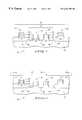
- FIG. 1is a cross-sectional view of a semiconductor wafer fragment at one processing step in accordance with the invention.
- FIG. 2is a cross-sectional view of the FIG. 1 semiconductor wafer fragment at a processing step subsequent to that shown by FIG. 1 .
- FIG. 3is a cross-sectional view of the FIG. 1 semiconductor wafer fragment at a processing step subsequent to that shown by FIG. 2 .
- FIG. 4is a cross-sectional view of the FIG. 1 semiconductor wafer fragment at a processing step subsequent to that shown by FIG. 3 .
- FIG. 5is a cross-sectional view of the FIG. 1 semiconductor wafer fragment at a processing step subsequent to that shown by FIG. 4 .
- FIG. 6is a cross-sectional view of the FIG. 1 semiconductor wafer fragment at a processing step subsequent to that shown by FIG. 5 .
- FIG. 7is a cross-sectional view of the FIG. 1 semiconductor wafer fragment at a processing step subsequent to that shown by FIG. 6 .
- FIG. 8is a cross-sectional view of the FIG. 1 semiconductor wafer fragment at a processing step subsequent to that shown by FIG. 7 .
- FIG. 9is a cross-sectional view of the FIG. 1 semiconductor wafer fragment at a processing step subsequent to that shown by FIG. 8 .
- FIG. 10is a cross-sectional view of the FIG. 1 semiconductor wafer fragment at a processing step subsequent to that shown by FIG. 9 .
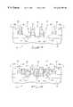
- FIG. 11is an enlarged plan view of a fragmentary portion of a peripheral circuitry area of a semiconductor wafer fragment at one processing step in accordance with the invention.
- FIG. 12is a view along line 12 — 12 in FIG. 11 and corresponds to the FIG. 5 processing step.
- FIG. 13is view of the FIG. 12 peripheral circuitry area fragmentary portion at a processing step subsequent to that shown by FIG. 12, and one which corresponds to the FIG. 6 processing step.
- FIG. 14is a cross-sectional view of the FIG. 1 semiconductor wafer fragment at a processing step subsequent to that shown by FIG. 10 .
- a semiconductive substrate in processis indicated generally with reference number 10 .
- Suchis comprised of a bulk monocrystalline silicon substrate 12 having various layers deposited or otherwise formed thereover.
- the term “semiconductive substrate”is defined to mean any construction comprising semiconductive material, including, but not limited to, bulk semiconductive materials such as a semiconductive wafer (either alone or in assemblies comprising other materials thereon), and semiconductive material layers (either alone or in assemblies comprising other materials).
- substraterefers to any supporting structure, including, but not limited to, the semiconductive substrates described above.
- a plurality of conductive lines 14 , 16 , 18 and 20are formed over substrate 10 .
- conductive lines 14 , 20are formed over field oxide or field isolation regions 22 , 24 respectively.
- Conductive lines 16 , 18are formed over a substrate active area 40 .
- Conductive lines 14 - 20are preferably anisotropically etched and include a polysilicon layer 26 , a silicide layer 28 thereatop, and a suitable protective insulative capping layer 30 atop silicide layer 28 .
- Suitable sidewall spacers 32are formed over respective sidewalls of the conductive lines.
- Other conductive line constructionsare possible. As so formed, conductive lines 14 - 20 are laterally spaced apart over substrate 10 and define therebetween respective diffusion regions or circuit nodes 34 , 36 and 38 with which electrical connection is to be made.
- a portion of a memory array areais designated generally by reference numeral 42 . Such is defined relative to substrate 10 and comprises, in accordance with a preferred aspect of this invention, a portion of a DRAM memory array.
- the preferred DRAM memory arrayalso includes a peripheral circuitry area which is operably associated with memory array area 42 and described in more detail below.
- a first layer 44is formed over substrate 10 .
- Layer 44preferably comprises a first oxide layer of borophosphosilicate glass (BPSG).
- BPSGborophosphosilicate glass
- Layer 44is subsequently planarized through mechanical abrasion of the substrate or a suitable dry etch.
- An exemplary implementationis chemical-mechanical planarization which effectively provides a generally planar first layer surface 45 , the plane of which is diagrammatically indicated at 45 a.
- first layer 44is patterned and etched to form openings 46 , 48 and 50 to respective circuit nodes 34 , 36 and 38 .
- Opening 46is disposed between conductive lines 14 , 16 .
- Opening 48is disposed between conductive lines 16 , 18 .
- Opening 50is disposed between conductive lines 18 , 20 .
- Openings 46 and 50define openings in which capacitor containers are to be formed.
- Opening 48defines an opening in which a bit line contact is to be formed between the capacitor containers.
- first material 52is formed over substrate 10 and between the conductive lines.
- such materialis electrically conductive and is formed outwardly of and in electrical communication with respective circuit nodes 34 , 36 , and 38 .
- such materialcomprises a conductively doped silicon or polysilicon layer.
- first material 52is provided first to be substantially coplanar with planar first layer surface 45 . Such is accomplished by first depositing material 52 and subsequently planarizing the material, as by suitable mechanical planarization or a dry etch so that it is coplanar with first layer surface 45 . Subsequently, a wet etch of material 52 substantially selective to adjacent BPSG layer 44 can be conducted to clean the outwardly exposed surface of material 52 and to recess the material to a point below planar first layer surface 45 as shown.
- FIG. 11shows a fragmentary portion of a peripheral circuitry area at 100 which is formed relative to substrate 10 .
- Peripheral circuitry area 100includes at least one active contact area 112 (shown in dashed lines) formed thereover to which electrical connection is desired to be made relative to an elevationally higher conductive line.
- Area 112defines a length dimension L and a width dimension W and constitutes a location which is remote on the substrate relative to the memory array.
- two conductive lines 114 , 116are shown extending generally widthwise of area 112 .
- such linesare overlaid by one or more layers such as an electrically insulative BPSG layer 44 (FIGS. 12, 13 ). Atop such layers, other conductive lines such as lengthwise-running lines 118 , 120 are formed (FIG. 11 ). In this example, an electrical connection is desired between conductive line 118 and underlying active area 112 . It is possible, however, to form a desired electrical connection as described below at a peripheral circuitry area location which is not between the illustrated conductive lines 114 , 116 . For example, such electrical connection can be made at an isolated peripheral circuitry area location.
- a conductive peripheral line extension or elongated stringer 122is formed to extend across a substantial portion of width dimension W.
- Line extension 122is connected with line 118 via a contact 121 .
- line extension or stringer 122comprises the same conductive material 52 (FIG. 4) which is also formed at the same time over memory array area 42 .
- FIG. 12is a view taken along line 12 — 12 in FIG. 11 and shows conductive material 52 formed between conductive lines 114 , 116 .
- a refractory metal layer 54is formed over substrate 10 and the exposed outer surface of polysilicon layer 52 .
- exemplary refractory metalsinclude titanium, cobalt, molybdenum and tantalum.
- silicide layer 56defines a second conductive material which is formed over the first conductive material 52 . Accordingly, the second conductive material is different from the first conductive material and is preferably more conductive than the first conductive material.
- silicide layer 56comprises a silicide formed from a reaction between a refractory metal layer and the first conductive material (FIG. 5 ). With respect to line extension 122 (FIGS. 11 and 13 ), such comprises at least one conductive line which is formed over the peripheral circuitry area and which includes at least some of the silicide mentioned above.
- Unreacted refractory metal layer 54is subsequently stripped as by a suitable wet etch.
- An exemplary etchcomprising H 2 O: H 2 O 2 : NH 4 OH (5:1:1) suitably removes unreacted titanium while not etching the resultant silicide. Such etch also does not etch the BPSG layer (FIG. 6 ).
- a plasma etch or suitable mechanical polishingcan be used to remove the unreacted metal.
- extension 122 of FIGS. 11 and 13provides reduced resistance in the connection between line 118 and active area 112 . This is most evident from FIG. 11 which shows that the line extension extends across a substantial entirety of the width dimension of the active area 112 . Moreover, the preferred conductive extension construction has a reduced resistance due in part to the presence of the silicide component of the extension. Additionally in some circumstances, it is desirable to heavily dope the material from which extension 122 is formed. Such provides a source of dopants for the underlying active area with outdiffusion therefrom serving to dope the desired area, such as diffusion region 124 in FIGS. 12 and 13. However, such outdiffusion can also affect or impact peripheral transistor operation in a negative manner.
- the silicide component of the above described line extensioneffectively reduces undesirable outdiffusion elevationally outward relative to peripheral transistors and enables desirable outdiffusion to underlying active areas.
- a masking layer 60is formed over the second conductive layer or silicide layer 56 and first insulative layer 44 .
- masking layer 60comprises an insulative dielectric layer.
- Layers 52 , 56 and 60constitute a plurality of layers which are formed on or over substrate 10 . In the illustrated and preferred embodiment, such layers are three in number and comprise different materials.
- Layer 56constitutes a conductive layer which is elevationally interposed between an upper insulating layer 60 and a lower conductive layer 52 . According to the implementation described in connection with FIGS. 11-13, an interposed layer 56 is also formed in at least one other substrate location, an exemplary location being between conductive lines 114 , 116 of FIG. 13 .
- a layer of photoresist 63is formed over substrate 10 and suitably patterned as shown to form or define openings 62 , 64 .
- a plurality of capacitor container openings 62 , 64are etched through layer 60 (FIG. 9) and layer 56 (FIG. 10) in accordance with a preferred aspect of the invention.
- layer 60comprises a first material
- layer 56comprises a second material which is different from the first material.
- a first of the materialshere unmasked portions of layer 60 elevationally below openings 62 , 64 , is etched to a degree sufficient to outwardly expose at least some, and preferably all, of the outer upper surface of silicide layer 56 (the second of the materials).
- such etchcomprises a first etching composition or chemistry which, upon detection of and responsive to the outward exposure of layer 56 , is changed to a second etching composition or chemistry which is different from the first etching composition or chemistry.
- the second of the materialshere unmasked portions of layer 56 elevationally below first capacitor container part 66 , is etched as shown in FIG. 10 to a degree sufficient to outwardly expose at least a portion, and preferably substantially all, of an upper outer surface of material 52 .
- remaining material 52comprises a third material a portion of which is outwardly exposed by the second etching composition or chemistry.
- such third materialis preferably electrically conductive and forms an electrical connection with conductively doped semiconductor material of the substrate.
- an etchis conducted through masking layer 60 substantially selective relative to the second conductive material 56 (FIG. 9 ). Accordingly, an upper insulating layer is etched or removed substantially selective relative to interposed conductive layer 56 to form capacitor container first portion 66 . Such etch is preferably conducted to a degree sufficient to outwardly expose elevationally lower layer 56 .
- masking layer 60is etched downwardly using a first etch chemistry with an oxide component suitable for etching the BPSG material from which layer 60 is formed. Preferably, such etch is conducted to degree which is sufficient to outwardly expose at least a surface of silicide layer 56 .
- FIG. 10shows the resultant etch of elevationally lower layer 56 (FIG. 9 ).
- second conductive material 56is etched through capacitor container first portions 66 and respective openings 62 , 64 substantially selective relative to remaining first material 52 .
- such etchoutwardly exposes the first conductive material.
- such etchis conducted to be substantially selective relative to the first conductive material.
- such outward exposure of the first conductive materialcan be detected and the second etch can be terminated.
- Such second etchpreferably comprises etching the interposed conductive layer 56 substantially selective relative to the lower conductive layer 52 to form capacitor container second portions 68 .
- a third electrically conductive material 70is formed in respective openings 62 , 64 as shown in FIG. 14, and forms an electrical connection with material 52 .
- Suchcomprises a further processing step in which suitable capacitor storage nodes are formed within and relative to the above described capacitor containers.
- Subsequent processing to form suitable capacitorscan now take place in accordance with conventional semiconductor processing methods such as those which are incorporated by reference above or with methods to be developed in the future.
- the peripheral circuitry areas of FIGS. 11-13can be masked during the above processing.
- a composite stack of conductive materialforms a buried contact interconnecting plug or layer 57 (FIGS. 10 and 14 ).
- plug layeris constituted by an inner conductive polysilicon portion (the middle one of remaining layer 52 ) which is disposed elevationally below insulating dielectric layer 60 and adjacent node location 36 .
- plug 57includes an outer silicide portion 56 which is formed atop or over the inner conductive portion.
- at least one and preferably two capacitor container contactsare disposed, one on either side of the middle layer 52 .
- peripheral line extension or conductive extension 122is formed from the same material and preferably during the same processing steps from and during which the buried contact interconnecting plug layer is formed.
Landscapes
- Engineering & Computer Science (AREA)
- Manufacturing & Machinery (AREA)
- Semiconductor Memories (AREA)
- Internal Circuitry In Semiconductor Integrated Circuit Devices (AREA)
Abstract
Description
Claims (15)
Priority Applications (4)
| Application Number | Priority Date | Filing Date | Title |
|---|---|---|---|
| US09/087,114US6261899B1 (en) | 1997-03-13 | 1998-05-29 | Semiconductor processing methods of forming integrated circuitry memory devices, methods of forming capacitor containers, methods of making electrical connection to circuit nodes and related integrated circuitry |
| US09/884,950US6583002B2 (en) | 1997-03-13 | 2001-06-20 | Semiconductor processing methods of forming integrated circuitry memory devices, methods of forming capacitor containers, methods of making electrical connection to circuit nodes and related integrated circuitry |
| US10/209,269US6611018B2 (en) | 1997-03-13 | 2002-07-30 | Semiconductor processing methods of forming integrated circuitry memory devices, methods of forming capacitor containers, methods of making electrical connection to circuit nodes and related integrated circuitry |
| US10/315,428US6653187B2 (en) | 1997-03-13 | 2002-12-09 | Semiconductor processing methods |
Applications Claiming Priority (2)
| Application Number | Priority Date | Filing Date | Title |
|---|---|---|---|
| US08/816,621US5998257A (en) | 1997-03-13 | 1997-03-13 | Semiconductor processing methods of forming integrated circuitry memory devices, methods of forming capacitor containers, methods of making electrical connection to circuit nodes and related integrated circuitry |
| US09/087,114US6261899B1 (en) | 1997-03-13 | 1998-05-29 | Semiconductor processing methods of forming integrated circuitry memory devices, methods of forming capacitor containers, methods of making electrical connection to circuit nodes and related integrated circuitry |
Related Parent Applications (1)
| Application Number | Title | Priority Date | Filing Date |
|---|---|---|---|
| US08/816,621DivisionUS5998257A (en) | 1997-03-13 | 1997-03-13 | Semiconductor processing methods of forming integrated circuitry memory devices, methods of forming capacitor containers, methods of making electrical connection to circuit nodes and related integrated circuitry |
Related Child Applications (1)
| Application Number | Title | Priority Date | Filing Date |
|---|---|---|---|
| US09/884,950ContinuationUS6583002B2 (en) | 1997-03-13 | 2001-06-20 | Semiconductor processing methods of forming integrated circuitry memory devices, methods of forming capacitor containers, methods of making electrical connection to circuit nodes and related integrated circuitry |
Publications (1)
| Publication Number | Publication Date |
|---|---|
| US6261899B1true US6261899B1 (en) | 2001-07-17 |
Family
ID=25221160
Family Applications (9)
| Application Number | Title | Priority Date | Filing Date |
|---|---|---|---|
| US08/816,621Expired - LifetimeUS5998257A (en) | 1997-03-13 | 1997-03-13 | Semiconductor processing methods of forming integrated circuitry memory devices, methods of forming capacitor containers, methods of making electrical connection to circuit nodes and related integrated circuitry |
| US08/970,345Expired - LifetimeUS6175146B1 (en) | 1997-03-13 | 1997-11-14 | Semiconductor processing methods of forming integrated circuitry memory devices, methods of forming capacitor containers, methods of making electrical connection to circuit nodes and related integrated circuitry |
| US09/087,114Expired - LifetimeUS6261899B1 (en) | 1997-03-13 | 1998-05-29 | Semiconductor processing methods of forming integrated circuitry memory devices, methods of forming capacitor containers, methods of making electrical connection to circuit nodes and related integrated circuitry |
| US09/235,568Expired - LifetimeUS6281070B1 (en) | 1997-03-13 | 1999-01-22 | Semiconductor processing methods of forming integrated circuitry memory devices, methods of forming capacitor containers, methods of making electrical connection to circuit nodes and related integrated circuitry |
| US09/592,441Expired - LifetimeUS6424043B1 (en) | 1997-03-13 | 2000-06-12 | Semiconductor processing methods of forming integrated circuitry memory devices, methods of forming capacitor containers, methods of making electrical connection to circuit nodes and related integrated circuitry |
| US09/863,340Expired - LifetimeUS6495410B2 (en) | 1997-03-13 | 2001-05-22 | Semiconductor processing methods of forming integrated circuitry memory devices, methods of forming capacitor containers, methods of making electrical connection to circuit nodes and related integrated circuitry |
| US09/884,950Expired - LifetimeUS6583002B2 (en) | 1997-03-13 | 2001-06-20 | Semiconductor processing methods of forming integrated circuitry memory devices, methods of forming capacitor containers, methods of making electrical connection to circuit nodes and related integrated circuitry |
| US10/209,269Expired - LifetimeUS6611018B2 (en) | 1997-03-13 | 2002-07-30 | Semiconductor processing methods of forming integrated circuitry memory devices, methods of forming capacitor containers, methods of making electrical connection to circuit nodes and related integrated circuitry |
| US10/315,428Expired - LifetimeUS6653187B2 (en) | 1997-03-13 | 2002-12-09 | Semiconductor processing methods |
Family Applications Before (2)
| Application Number | Title | Priority Date | Filing Date |
|---|---|---|---|
| US08/816,621Expired - LifetimeUS5998257A (en) | 1997-03-13 | 1997-03-13 | Semiconductor processing methods of forming integrated circuitry memory devices, methods of forming capacitor containers, methods of making electrical connection to circuit nodes and related integrated circuitry |
| US08/970,345Expired - LifetimeUS6175146B1 (en) | 1997-03-13 | 1997-11-14 | Semiconductor processing methods of forming integrated circuitry memory devices, methods of forming capacitor containers, methods of making electrical connection to circuit nodes and related integrated circuitry |
Family Applications After (6)
| Application Number | Title | Priority Date | Filing Date |
|---|---|---|---|
| US09/235,568Expired - LifetimeUS6281070B1 (en) | 1997-03-13 | 1999-01-22 | Semiconductor processing methods of forming integrated circuitry memory devices, methods of forming capacitor containers, methods of making electrical connection to circuit nodes and related integrated circuitry |
| US09/592,441Expired - LifetimeUS6424043B1 (en) | 1997-03-13 | 2000-06-12 | Semiconductor processing methods of forming integrated circuitry memory devices, methods of forming capacitor containers, methods of making electrical connection to circuit nodes and related integrated circuitry |
| US09/863,340Expired - LifetimeUS6495410B2 (en) | 1997-03-13 | 2001-05-22 | Semiconductor processing methods of forming integrated circuitry memory devices, methods of forming capacitor containers, methods of making electrical connection to circuit nodes and related integrated circuitry |
| US09/884,950Expired - LifetimeUS6583002B2 (en) | 1997-03-13 | 2001-06-20 | Semiconductor processing methods of forming integrated circuitry memory devices, methods of forming capacitor containers, methods of making electrical connection to circuit nodes and related integrated circuitry |
| US10/209,269Expired - LifetimeUS6611018B2 (en) | 1997-03-13 | 2002-07-30 | Semiconductor processing methods of forming integrated circuitry memory devices, methods of forming capacitor containers, methods of making electrical connection to circuit nodes and related integrated circuitry |
| US10/315,428Expired - LifetimeUS6653187B2 (en) | 1997-03-13 | 2002-12-09 | Semiconductor processing methods |
Country Status (1)
| Country | Link |
|---|---|
| US (9) | US5998257A (en) |
Cited By (8)
| Publication number | Priority date | Publication date | Assignee | Title |
|---|---|---|---|---|
| US6486060B2 (en) | 1998-09-03 | 2002-11-26 | Micron Technology, Inc. | Low resistance semiconductor process and structures |
| US20030047789A1 (en)* | 2001-09-07 | 2003-03-13 | Hidenori Sato | Semiconductor device and method of manufacturing the same |
| US20040043619A1 (en)* | 2002-08-29 | 2004-03-04 | Rhodes Howard E. | Method for forming conductive material in opening and structures regarding same |
| US20050009343A1 (en)* | 2003-07-10 | 2005-01-13 | Fishburn Fredrick D. | Method and structure for a self-aligned silicided word line and polysilicon plug during the formation of a semiconductor device |
| US20070032059A1 (en)* | 2005-08-02 | 2007-02-08 | Harry Hedler | Method of manufacturing a semiconductor structure having a wafer through-contact and a corresponding semiconductor structure |
| CN100403959C (en)* | 2003-02-04 | 2008-07-23 | 奥里尔股份有限公司 | Box including hinges with loops and hooks |
| US20100059805A1 (en)* | 2008-09-10 | 2010-03-11 | Samsung Electronics Co., Ltd | Semiconductor device |
| US20100099263A1 (en)* | 2008-10-20 | 2010-04-22 | Applied Materials, Inc. | Nf3/h2 remote plasma process with high etch selectivity of psg/bpsg over thermal oxide and low density surface defects |
Families Citing this family (44)
| Publication number | Priority date | Publication date | Assignee | Title |
|---|---|---|---|---|
| US6395613B1 (en) | 2000-08-30 | 2002-05-28 | Micron Technology, Inc. | Semiconductor processing methods of forming a plurality of capacitors on a substrate, bit line contacts and method of forming bit line contacts |
| JP3161354B2 (en)* | 1997-02-07 | 2001-04-25 | 日本電気株式会社 | Semiconductor device and manufacturing method thereof |
| KR100277086B1 (en)* | 1999-01-02 | 2000-12-15 | 윤종용 | Semiconductor device and method of manufacturing the same |
| JP2000286397A (en)* | 1999-03-30 | 2000-10-13 | Nec Corp | Method for manufacturing semiconductor device |
| US6365453B1 (en)* | 1999-06-16 | 2002-04-02 | Micron Technology, Inc. | Method and structure for reducing contact aspect ratios |
| TW408446B (en)* | 1999-06-22 | 2000-10-11 | United Microelectronics Corp | The manufacture method of the node contact |
| US7217977B2 (en) | 2004-04-19 | 2007-05-15 | Hrl Laboratories, Llc | Covert transformation of transistor properties as a circuit protection method |
| US6232168B1 (en)* | 2000-08-25 | 2001-05-15 | Micron Technology, Inc. | Memory circuitry and method of forming memory circuitry |
| JP4651169B2 (en)* | 2000-08-31 | 2011-03-16 | 富士通株式会社 | Semiconductor device and manufacturing method thereof |
| US6815816B1 (en) | 2000-10-25 | 2004-11-09 | Hrl Laboratories, Llc | Implanted hidden interconnections in a semiconductor device for preventing reverse engineering |
| TW460954B (en)* | 2000-11-09 | 2001-10-21 | United Microelectronics Corp | Manufacturing method of bottom electrode of semiconductor device |
| US6294426B1 (en)* | 2001-01-19 | 2001-09-25 | Taiwan Semiconductor Manufacturing Company | Method of fabricating a capacitor under bit line structure with increased capacitance without increasing the aspect ratio for a dry etched bit line contact hole |
| US7294935B2 (en) | 2001-01-24 | 2007-11-13 | Hrl Laboratories, Llc | Integrated circuits protected against reverse engineering and method for fabricating the same using an apparent metal contact line terminating on field oxide |
| US6545904B2 (en)* | 2001-03-16 | 2003-04-08 | Micron Technology, Inc. | 6f2 dram array, a dram array formed on a semiconductive substrate, a method of forming memory cells in a 6f2 dram array and a method of isolating a single row of memory cells in a 6f2 dram array |
| US6411555B1 (en) | 2001-03-19 | 2002-06-25 | Micron Technology, Inc. | Reference charge generator, a method for providing a reference charge from a reference charge generator, a method of operating a reference charge generator and a dram memory circuit formed using memory cells having an area of 6f2 |
| US6740942B2 (en) | 2001-06-15 | 2004-05-25 | Hrl Laboratories, Llc. | Permanently on transistor implemented using a double polysilicon layer CMOS process with buried contact |
| US6514815B2 (en)* | 2001-06-15 | 2003-02-04 | Silicon Integrated Systems Corp. | Method for fabricating polysilicon capacitor |
| US6774413B2 (en) | 2001-06-15 | 2004-08-10 | Hrl Laboratories, Llc | Integrated circuit structure with programmable connector/isolator |
| US6897535B2 (en) | 2002-05-14 | 2005-05-24 | Hrl Laboratories, Llc | Integrated circuit with reverse engineering protection |
| US7049667B2 (en) | 2002-09-27 | 2006-05-23 | Hrl Laboratories, Llc | Conductive channel pseudo block process and circuit to inhibit reverse engineering |
| US6979606B2 (en) | 2002-11-22 | 2005-12-27 | Hrl Laboratories, Llc | Use of silicon block process step to camouflage a false transistor |
| WO2004055868A2 (en) | 2002-12-13 | 2004-07-01 | Hrl Laboratories, Llc | Integrated circuit modification using well implants |
| JP4151474B2 (en)* | 2003-05-13 | 2008-09-17 | 信越半導体株式会社 | Method for producing single crystal and single crystal |
| US7375033B2 (en)* | 2003-11-14 | 2008-05-20 | Micron Technology, Inc. | Multi-layer interconnect with isolation layer |
| US7092603B2 (en)* | 2004-03-03 | 2006-08-15 | Fujitsu Limited | Optical bridge for chip-to-board interconnection and methods of fabrication |
| US7242063B1 (en) | 2004-06-29 | 2007-07-10 | Hrl Laboratories, Llc | Symmetric non-intrusive and covert technique to render a transistor permanently non-operable |
| US7312120B2 (en) | 2004-09-01 | 2007-12-25 | Micron Technology, Inc. | Method for obtaining extreme selectivity of metal nitrides and metal oxides |
| KR100668833B1 (en)* | 2004-12-17 | 2007-01-16 | 주식회사 하이닉스반도체 | Capacitor Manufacturing Method of Semiconductor Device |
| US7888702B2 (en)* | 2005-04-15 | 2011-02-15 | Semiconductor Energy Laboratory Co., Ltd. | Display device and manufacturing method of the display device |
| US7371627B1 (en)* | 2005-05-13 | 2008-05-13 | Micron Technology, Inc. | Memory array with ultra-thin etched pillar surround gate access transistors and buried data/bit lines |
| US7120046B1 (en)* | 2005-05-13 | 2006-10-10 | Micron Technology, Inc. | Memory array with surrounding gate access transistors and capacitors with global and staggered local bit lines |
| US7858458B2 (en) | 2005-06-14 | 2010-12-28 | Micron Technology, Inc. | CMOS fabrication |
| US7541632B2 (en)* | 2005-06-14 | 2009-06-02 | Micron Technology, Inc. | Relaxed-pitch method of aligning active area to digit line |
| US7888721B2 (en)* | 2005-07-06 | 2011-02-15 | Micron Technology, Inc. | Surround gate access transistors with grown ultra-thin bodies |
| US7768051B2 (en)* | 2005-07-25 | 2010-08-03 | Micron Technology, Inc. | DRAM including a vertical surround gate transistor |
| US7696567B2 (en) | 2005-08-31 | 2010-04-13 | Micron Technology, Inc | Semiconductor memory device |
| US7557032B2 (en)* | 2005-09-01 | 2009-07-07 | Micron Technology, Inc. | Silicided recessed silicon |
| US7687342B2 (en)* | 2005-09-01 | 2010-03-30 | Micron Technology, Inc. | Method of manufacturing a memory device |
| US7416943B2 (en)* | 2005-09-01 | 2008-08-26 | Micron Technology, Inc. | Peripheral gate stacks and recessed array gates |
| US7358172B2 (en)* | 2006-02-21 | 2008-04-15 | International Business Machines Corporation | Poly filled substrate contact on SOI structure |
| US8168487B2 (en) | 2006-09-28 | 2012-05-01 | Hrl Laboratories, Llc | Programmable connection and isolation of active regions in an integrated circuit using ambiguous features to confuse a reverse engineer |
| US7923373B2 (en) | 2007-06-04 | 2011-04-12 | Micron Technology, Inc. | Pitch multiplication using self-assembling materials |
| TWI557850B (en)* | 2015-02-24 | 2016-11-11 | 華邦電子股份有限公司 | Memory device and method of fabricating the same |
| US10651177B1 (en)* | 2018-11-07 | 2020-05-12 | Nanya Technology Corporation | Semiconductor device and method of forming the same |
Citations (32)
| Publication number | Priority date | Publication date | Assignee | Title |
|---|---|---|---|---|
| US5170233A (en) | 1991-03-19 | 1992-12-08 | Micron Technology, Inc. | Method for increasing capacitive surface area of a conductive material in semiconductor processing and stacked memory cell capacitor |
| US5206183A (en) | 1992-02-19 | 1993-04-27 | Micron Technology, Inc. | Method of forming a bit line over capacitor array of memory cells |
| US5227325A (en) | 1992-04-02 | 1993-07-13 | Micron Technology, Incl | Method of forming a capacitor |
| US5229326A (en) | 1992-06-23 | 1993-07-20 | Micron Technology, Inc. | Method for making electrical contact with an active area through sub-micron contact openings and a semiconductor device |
| US5244826A (en) | 1992-04-16 | 1993-09-14 | Micron Technology, Inc. | Method of forming an array of finned memory cell capacitors on a semiconductor substrate |
| US5318927A (en) | 1993-04-29 | 1994-06-07 | Micron Semiconductor, Inc. | Methods of chemical-mechanical polishing insulating inorganic metal oxide materials |
| US5338700A (en) | 1993-04-14 | 1994-08-16 | Micron Semiconductor, Inc. | Method of forming a bit line over capacitor array of memory cells |
| US5401681A (en) | 1993-02-12 | 1995-03-28 | Micron Technology, Inc. | Method of forming a bit line over capacitor array of memory cells |
| US5438011A (en) | 1995-03-03 | 1995-08-01 | Micron Technology, Inc. | Method of forming a capacitor using a photoresist contact sidewall having standing wave ripples |
| US5444013A (en) | 1994-11-02 | 1995-08-22 | Micron Technology, Inc. | Method of forming a capacitor |
| US5498562A (en) | 1993-04-07 | 1996-03-12 | Micron Technology, Inc. | Semiconductor processing methods of forming stacked capacitors |
| US5506166A (en)* | 1993-04-02 | 1996-04-09 | Micron Technology, Inc. | Method for forming capacitor compatible with high dielectric constant materials having a low contact resistance layer |
| US5538922A (en) | 1991-06-03 | 1996-07-23 | Motorola, Inc. | Method for forming contact to a semiconductor device |
| US5563089A (en) | 1994-07-20 | 1996-10-08 | Micron Technology, Inc. | Method of forming a bit line over capacitor array of memory cells and an array of bit line over capacitor array of memory cells |
| US5581093A (en) | 1991-03-15 | 1996-12-03 | Mitsubishi Denki Kabushiki Kaisha | Contact structure of an interconnection layer for a semiconductor device and a multilayer interconnection SRAM |
| US5591659A (en) | 1992-04-16 | 1997-01-07 | Fujitsu Limited | Process of producing a semiconductor device in which a height difference between a memory cell area and a peripheral area is eliminated |
| US5600177A (en) | 1993-12-28 | 1997-02-04 | Nec Corporation | Semiconductor device having an electrically conductive layer including a polycrystalline layer containing an impurity and a metallic silicide layer |
| US5604147A (en) | 1995-05-12 | 1997-02-18 | Micron Technology, Inc. | Method of forming a cylindrical container stacked capacitor |
| US5605857A (en) | 1993-02-12 | 1997-02-25 | Micron Technology, Inc. | Method of forming a bit line over capacitor array of memory cells and an array of bit line over capacitor array of memory cells |
| US5610101A (en) | 1993-10-18 | 1997-03-11 | Nec Corporation | Method of manufacturing a semiconductor device having improved coverage with increased wiring layers |
| US5661064A (en) | 1995-11-13 | 1997-08-26 | Micron Technology, Inc. | Method of forming a capacitor having container members |
| US5665626A (en) | 1995-03-16 | 1997-09-09 | International Business Machines Corporation | Method of making a chimney capacitor |
| US5677227A (en) | 1996-09-09 | 1997-10-14 | Vanguard International Semiconductor Corporation | Method of fabricating single crown, extendible to triple crown, stacked capacitor structures, using a self-aligned capacitor node contact |
| US5688713A (en) | 1996-08-26 | 1997-11-18 | Vanguard International Semiconductor Corporation | Method of manufacturing a DRAM cell having a double-crown capacitor using polysilicon and nitride spacers |
| US5706164A (en) | 1996-07-17 | 1998-01-06 | Vangaurd International Semiconductor Corporation | Method of fabricating high density integrated circuits, containing stacked capacitor DRAM devices, using elevated trench isolation and isolation spacers |
| US5717250A (en)* | 1994-08-15 | 1998-02-10 | Micron Technology, Inc. | Sputter and CVD deposited titanium nitride barrier layer between a platinum layer and a polysilicon plug |
| US5786249A (en) | 1996-03-07 | 1998-07-28 | Micron Technology, Inc. | Method of forming dram circuitry on a semiconductor substrate |
| US5851896A (en)* | 1994-08-01 | 1998-12-22 | Texas Instruments Incorporated | Conductive exotic-nitride barrier layer for high-dielectric-constant material electrodes |
| US5905280A (en) | 1997-02-11 | 1999-05-18 | Micron Technology, Inc. | Capacitor structures, DRAM cell structures, methods of forming capacitors, methods of forming DRAM cells, and integrated circuits incorporating capacitor structures and DRAM cell structures |
| US5918122A (en) | 1997-02-11 | 1999-06-29 | Micron Technology, Inc. | Methods of forming integrated circuitry, DRAM cells and capacitors |
| US5981333A (en) | 1997-02-11 | 1999-11-09 | Micron Technology, Inc. | Methods of forming capacitors and DRAM arrays |
| US6083831A (en) | 1996-03-26 | 2000-07-04 | Micron Technology, Inc. | Semiconductor processing method of forming a contact pedestal, of forming a storage node of a capacitor |
Family Cites Families (8)
| Publication number | Priority date | Publication date | Assignee | Title |
|---|---|---|---|---|
| US5391511A (en) | 1992-02-19 | 1995-02-21 | Micron Technology, Inc. | Semiconductor processing method of producing an isolated polysilicon lined cavity and a method of forming a capacitor |
| JPH07221076A (en) | 1994-02-07 | 1995-08-18 | Nec Corp | Etching method and apparatus used for it |
| US6218237B1 (en) | 1996-01-03 | 2001-04-17 | Micron Technology, Inc. | Method of forming a capacitor |
| US5604146A (en) | 1996-06-10 | 1997-02-18 | Vanguard International Semiconductor Corporation | Method to fabricate a semiconductor memory device having an E-shaped storage node |
| JPH1012838A (en)* | 1996-06-21 | 1998-01-16 | Mitsubishi Electric Corp | Semiconductor device |
| US6238971B1 (en) | 1997-02-11 | 2001-05-29 | Micron Technology, Inc. | Capacitor structures, DRAM cell structures, and integrated circuitry, and methods of forming capacitor structures, integrated circuitry and DRAM cell structures |
| US6214727B1 (en) | 1997-02-11 | 2001-04-10 | Micron Technology, Inc. | Conductive electrical contacts, capacitors, DRAMs, and integrated circuitry, and methods of forming conductive electrical contacts, capacitors, DRAMs, and integrated circuitry |
| US5851891A (en) | 1997-04-21 | 1998-12-22 | Advanced Micro Devices, Inc. | IGFET method of forming with silicide contact on ultra-thin gate |
- 1997
- 1997-03-13USUS08/816,621patent/US5998257A/ennot_activeExpired - Lifetime
- 1997-11-14USUS08/970,345patent/US6175146B1/ennot_activeExpired - Lifetime
- 1998
- 1998-05-29USUS09/087,114patent/US6261899B1/ennot_activeExpired - Lifetime
- 1999
- 1999-01-22USUS09/235,568patent/US6281070B1/ennot_activeExpired - Lifetime
- 2000
- 2000-06-12USUS09/592,441patent/US6424043B1/ennot_activeExpired - Lifetime
- 2001
- 2001-05-22USUS09/863,340patent/US6495410B2/ennot_activeExpired - Lifetime
- 2001-06-20USUS09/884,950patent/US6583002B2/ennot_activeExpired - Lifetime
- 2002
- 2002-07-30USUS10/209,269patent/US6611018B2/ennot_activeExpired - Lifetime
- 2002-12-09USUS10/315,428patent/US6653187B2/ennot_activeExpired - Lifetime
Patent Citations (35)
| Publication number | Priority date | Publication date | Assignee | Title |
|---|---|---|---|---|
| US5581093A (en) | 1991-03-15 | 1996-12-03 | Mitsubishi Denki Kabushiki Kaisha | Contact structure of an interconnection layer for a semiconductor device and a multilayer interconnection SRAM |
| US5170233A (en) | 1991-03-19 | 1992-12-08 | Micron Technology, Inc. | Method for increasing capacitive surface area of a conductive material in semiconductor processing and stacked memory cell capacitor |
| US5538922A (en) | 1991-06-03 | 1996-07-23 | Motorola, Inc. | Method for forming contact to a semiconductor device |
| US5206183A (en) | 1992-02-19 | 1993-04-27 | Micron Technology, Inc. | Method of forming a bit line over capacitor array of memory cells |
| US5227325A (en) | 1992-04-02 | 1993-07-13 | Micron Technology, Incl | Method of forming a capacitor |
| US5244826A (en) | 1992-04-16 | 1993-09-14 | Micron Technology, Inc. | Method of forming an array of finned memory cell capacitors on a semiconductor substrate |
| US5591659A (en) | 1992-04-16 | 1997-01-07 | Fujitsu Limited | Process of producing a semiconductor device in which a height difference between a memory cell area and a peripheral area is eliminated |
| US5323038A (en) | 1992-04-16 | 1994-06-21 | Micron Technology, Inc. | Array of finned memory cell capacitors on a semiconductor substrate |
| US5229326A (en) | 1992-06-23 | 1993-07-20 | Micron Technology, Inc. | Method for making electrical contact with an active area through sub-micron contact openings and a semiconductor device |
| US5401681A (en) | 1993-02-12 | 1995-03-28 | Micron Technology, Inc. | Method of forming a bit line over capacitor array of memory cells |
| US5605857A (en) | 1993-02-12 | 1997-02-25 | Micron Technology, Inc. | Method of forming a bit line over capacitor array of memory cells and an array of bit line over capacitor array of memory cells |
| US5506166A (en)* | 1993-04-02 | 1996-04-09 | Micron Technology, Inc. | Method for forming capacitor compatible with high dielectric constant materials having a low contact resistance layer |
| US5498562A (en) | 1993-04-07 | 1996-03-12 | Micron Technology, Inc. | Semiconductor processing methods of forming stacked capacitors |
| US6037218A (en) | 1993-04-07 | 2000-03-14 | Micron Technology, Inc. | Semiconductor processing methods of forming stacked capacitors |
| US5652164A (en) | 1993-04-07 | 1997-07-29 | Micron Technology, Inc. | Semiconductor processing methods of forming stacked capacitors |
| US5338700A (en) | 1993-04-14 | 1994-08-16 | Micron Semiconductor, Inc. | Method of forming a bit line over capacitor array of memory cells |
| US5318927A (en) | 1993-04-29 | 1994-06-07 | Micron Semiconductor, Inc. | Methods of chemical-mechanical polishing insulating inorganic metal oxide materials |
| US5610101A (en) | 1993-10-18 | 1997-03-11 | Nec Corporation | Method of manufacturing a semiconductor device having improved coverage with increased wiring layers |
| US5600177A (en) | 1993-12-28 | 1997-02-04 | Nec Corporation | Semiconductor device having an electrically conductive layer including a polycrystalline layer containing an impurity and a metallic silicide layer |
| US5563089A (en) | 1994-07-20 | 1996-10-08 | Micron Technology, Inc. | Method of forming a bit line over capacitor array of memory cells and an array of bit line over capacitor array of memory cells |
| US5851896A (en)* | 1994-08-01 | 1998-12-22 | Texas Instruments Incorporated | Conductive exotic-nitride barrier layer for high-dielectric-constant material electrodes |
| US5717250A (en)* | 1994-08-15 | 1998-02-10 | Micron Technology, Inc. | Sputter and CVD deposited titanium nitride barrier layer between a platinum layer and a polysilicon plug |
| US5444013A (en) | 1994-11-02 | 1995-08-22 | Micron Technology, Inc. | Method of forming a capacitor |
| US5438011A (en) | 1995-03-03 | 1995-08-01 | Micron Technology, Inc. | Method of forming a capacitor using a photoresist contact sidewall having standing wave ripples |
| US5665626A (en) | 1995-03-16 | 1997-09-09 | International Business Machines Corporation | Method of making a chimney capacitor |
| US5604147A (en) | 1995-05-12 | 1997-02-18 | Micron Technology, Inc. | Method of forming a cylindrical container stacked capacitor |
| US5661064A (en) | 1995-11-13 | 1997-08-26 | Micron Technology, Inc. | Method of forming a capacitor having container members |
| US5786249A (en) | 1996-03-07 | 1998-07-28 | Micron Technology, Inc. | Method of forming dram circuitry on a semiconductor substrate |
| US6083831A (en) | 1996-03-26 | 2000-07-04 | Micron Technology, Inc. | Semiconductor processing method of forming a contact pedestal, of forming a storage node of a capacitor |
| US5706164A (en) | 1996-07-17 | 1998-01-06 | Vangaurd International Semiconductor Corporation | Method of fabricating high density integrated circuits, containing stacked capacitor DRAM devices, using elevated trench isolation and isolation spacers |
| US5688713A (en) | 1996-08-26 | 1997-11-18 | Vanguard International Semiconductor Corporation | Method of manufacturing a DRAM cell having a double-crown capacitor using polysilicon and nitride spacers |
| US5677227A (en) | 1996-09-09 | 1997-10-14 | Vanguard International Semiconductor Corporation | Method of fabricating single crown, extendible to triple crown, stacked capacitor structures, using a self-aligned capacitor node contact |
| US5905280A (en) | 1997-02-11 | 1999-05-18 | Micron Technology, Inc. | Capacitor structures, DRAM cell structures, methods of forming capacitors, methods of forming DRAM cells, and integrated circuits incorporating capacitor structures and DRAM cell structures |
| US5918122A (en) | 1997-02-11 | 1999-06-29 | Micron Technology, Inc. | Methods of forming integrated circuitry, DRAM cells and capacitors |
| US5981333A (en) | 1997-02-11 | 1999-11-09 | Micron Technology, Inc. | Methods of forming capacitors and DRAM arrays |
Non-Patent Citations (9)
| Title |
|---|
| U.S. application Ser. No. 07/869,615, Doan et al. (now abandoned), filed Apr. 16, 1992. |
| U.S. application Ser. No. 08/044,824, Dennison et al. (now abandoned), filed Apr. 7, 1993. |
| U.S. application Ser. No. 08/078,616, Lee et al. (now abandoned), filed Jun. 17, 1993. |
| U.S. application Ser. No. 08/163,439, Dennison (now abandoned), filed Dec. 7, 1993. |
| U.S. application Ser. No. 08/582,385, Sandhu et al. (pending, see attached application & pending claims), filed Jan. 3, 1996. |
| U.S. application Ser. No. 08/622,591, Dennison (issued, see p. 2 and copy attached), filed Mar. 26, 1996. |
| U.S. application Ser. No. 08/798,242, Parekh et al. (pending, see attached application & pending claims), filed Feb. 11, 1997. |
| U.S. application Ser. No. 08/798,251, Parekh (pending, see attached application & pending claims), filed Feb. 11, 1997. |
| U.S. application Ser. No. 09/442,602, Dennison et al. (pending, see attached application & pending claims), filed Nov. 18, 1999. |
Cited By (19)
| Publication number | Priority date | Publication date | Assignee | Title |
|---|---|---|---|---|
| US7358568B2 (en) | 1998-09-03 | 2008-04-15 | Micron Technology, Inc. | Low resistance semiconductor process and structures |
| US6486060B2 (en) | 1998-09-03 | 2002-11-26 | Micron Technology, Inc. | Low resistance semiconductor process and structures |
| US6977418B2 (en) | 1998-09-03 | 2005-12-20 | Micron Technology, Inc. | Low resistance semiconductor process and structures |
| US20060097327A1 (en)* | 1998-09-03 | 2006-05-11 | Hermes Michael J | Low resistance semiconductor process and structures |
| US20030047789A1 (en)* | 2001-09-07 | 2003-03-13 | Hidenori Sato | Semiconductor device and method of manufacturing the same |
| US6825088B2 (en)* | 2001-09-07 | 2004-11-30 | Renesas Technology Corp. | E-RAM with cobalt silicide layer over source/drain of memory cell part and over source/drain and gate wiring of logic part |
| US20040043619A1 (en)* | 2002-08-29 | 2004-03-04 | Rhodes Howard E. | Method for forming conductive material in opening and structures regarding same |
| US6884692B2 (en) | 2002-08-29 | 2005-04-26 | Micron Technology, Inc. | Method for forming conductive material in opening and structures regarding same |
| US20050186779A1 (en)* | 2002-08-29 | 2005-08-25 | Micron Technology, Inc. | Method for forming conductive material in opening and structure regarding same |
| US7112508B2 (en) | 2002-08-29 | 2006-09-26 | Micron Technology, Inc. | Method for forming conductive material in opening and structure regarding same |
| CN100403959C (en)* | 2003-02-04 | 2008-07-23 | 奥里尔股份有限公司 | Box including hinges with loops and hooks |
| US20050009343A1 (en)* | 2003-07-10 | 2005-01-13 | Fishburn Fredrick D. | Method and structure for a self-aligned silicided word line and polysilicon plug during the formation of a semiconductor device |
| US20070164350A1 (en)* | 2003-07-10 | 2007-07-19 | Fishburn Frederick D | Method and structure for a self-aligned silicided word line and polysilicon plug during the formation of a semiconductor device |
| US7119024B2 (en) | 2003-07-10 | 2006-10-10 | Micron Technology, Inc. | Method and structure for a self-aligned silicided word line and polysilicon plug during the formation of a semiconductor device |
| US7501672B2 (en) | 2003-07-10 | 2009-03-10 | Micron Technology, Inc. | Method and structure for a self-aligned silicided word line and polysilicon plug during the formation of a semiconductor device |
| US20070032059A1 (en)* | 2005-08-02 | 2007-02-08 | Harry Hedler | Method of manufacturing a semiconductor structure having a wafer through-contact and a corresponding semiconductor structure |
| US20100059805A1 (en)* | 2008-09-10 | 2010-03-11 | Samsung Electronics Co., Ltd | Semiconductor device |
| US8334556B2 (en)* | 2008-09-10 | 2012-12-18 | Samsung Electronics Co., Ltd. | DRAM semiconductor device with pad electrode |
| US20100099263A1 (en)* | 2008-10-20 | 2010-04-22 | Applied Materials, Inc. | Nf3/h2 remote plasma process with high etch selectivity of psg/bpsg over thermal oxide and low density surface defects |
Also Published As
| Publication number | Publication date |
|---|---|
| US20010036698A1 (en) | 2001-11-01 |
| US6281070B1 (en) | 2001-08-28 |
| US6424043B1 (en) | 2002-07-23 |
| US20030082874A1 (en) | 2003-05-01 |
| US20010036701A1 (en) | 2001-11-01 |
| US6495410B2 (en) | 2002-12-17 |
| US6653187B2 (en) | 2003-11-25 |
| US6583002B2 (en) | 2003-06-24 |
| US5998257A (en) | 1999-12-07 |
| US6611018B2 (en) | 2003-08-26 |
| US20020192903A1 (en) | 2002-12-19 |
| US6175146B1 (en) | 2001-01-16 |
Similar Documents
| Publication | Publication Date | Title |
|---|---|---|
| US6261899B1 (en) | Semiconductor processing methods of forming integrated circuitry memory devices, methods of forming capacitor containers, methods of making electrical connection to circuit nodes and related integrated circuitry | |
| US7807569B2 (en) | Method of manufacturing a contact structure for a semiconductor device | |
| US6297525B1 (en) | Capacitor structures, DRAM cell structures, and integrated circuitry | |
| US6376301B2 (en) | Methods of forming a capacitor and methods of forming a monolithic integrated circuit | |
| US6486018B2 (en) | Methods of electrically contacting to conductive plugs, methods of forming contact openings, and methods of forming dynamic random access memory circuitry | |
| US6207574B1 (en) | Method for fabricating a DRAM cell storage node | |
| US20010014499A1 (en) | Methods of forming storage capacitors in integrated circuitry memory cells and integrated circuitry | |
| US6548852B2 (en) | Integrated circuitry and methods of forming circuitry | |
| US5409855A (en) | Process for forming a semiconductor device having a capacitor | |
| US6184079B1 (en) | Method for fabricating a semiconductor device | |
| US6097055A (en) | Capacitor and method for fabricating the same | |
| US6238968B1 (en) | Methods of forming integrated circuit capacitors having protected layers of HSG silicon therein | |
| US6544883B2 (en) | Method of manufacturing semiconductor device | |
| US5723374A (en) | Method for forming dielectric spacer to prevent poly stringer in stacked capacitor DRAM technology | |
| US6724054B1 (en) | Self-aligned contact formation using double SiN spacers | |
| US6359302B1 (en) | DRAM cells and integrated circuitry, and capacitor structures | |
| US6080622A (en) | Method for fabricating a DRAM cell capacitor including forming a conductive storage node by depositing and etching an insulative layer, filling with conductive material, and removing the insulative layer | |
| US20020192924A1 (en) | Methods of forming integrated circuit capacitors having U-shaped electrodes and capacitors formed thereby |
Legal Events
| Date | Code | Title | Description |
|---|---|---|---|
| FEPP | Fee payment procedure | Free format text:PAYOR NUMBER ASSIGNED (ORIGINAL EVENT CODE: ASPN); ENTITY STATUS OF PATENT OWNER: LARGE ENTITY | |
| STCF | Information on status: patent grant | Free format text:PATENTED CASE | |
| CC | Certificate of correction | ||
| FPAY | Fee payment | Year of fee payment:4 | |
| FPAY | Fee payment | Year of fee payment:8 | |
| FPAY | Fee payment | Year of fee payment:12 | |
| AS | Assignment | Owner name:U.S. BANK NATIONAL ASSOCIATION, AS COLLATERAL AGENT, CALIFORNIA Free format text:SECURITY INTEREST;ASSIGNOR:MICRON TECHNOLOGY, INC.;REEL/FRAME:038669/0001 Effective date:20160426 Owner name:U.S. BANK NATIONAL ASSOCIATION, AS COLLATERAL AGEN Free format text:SECURITY INTEREST;ASSIGNOR:MICRON TECHNOLOGY, INC.;REEL/FRAME:038669/0001 Effective date:20160426 | |
| AS | Assignment | Owner name:MORGAN STANLEY SENIOR FUNDING, INC., AS COLLATERAL AGENT, MARYLAND Free format text:PATENT SECURITY AGREEMENT;ASSIGNOR:MICRON TECHNOLOGY, INC.;REEL/FRAME:038954/0001 Effective date:20160426 Owner name:MORGAN STANLEY SENIOR FUNDING, INC., AS COLLATERAL Free format text:PATENT SECURITY AGREEMENT;ASSIGNOR:MICRON TECHNOLOGY, INC.;REEL/FRAME:038954/0001 Effective date:20160426 | |
| AS | Assignment | Owner name:U.S. BANK NATIONAL ASSOCIATION, AS COLLATERAL AGENT, CALIFORNIA Free format text:CORRECTIVE ASSIGNMENT TO CORRECT THE REPLACE ERRONEOUSLY FILED PATENT #7358718 WITH THE CORRECT PATENT #7358178 PREVIOUSLY RECORDED ON REEL 038669 FRAME 0001. ASSIGNOR(S) HEREBY CONFIRMS THE SECURITY INTEREST;ASSIGNOR:MICRON TECHNOLOGY, INC.;REEL/FRAME:043079/0001 Effective date:20160426 Owner name:U.S. BANK NATIONAL ASSOCIATION, AS COLLATERAL AGEN Free format text:CORRECTIVE ASSIGNMENT TO CORRECT THE REPLACE ERRONEOUSLY FILED PATENT #7358718 WITH THE CORRECT PATENT #7358178 PREVIOUSLY RECORDED ON REEL 038669 FRAME 0001. ASSIGNOR(S) HEREBY CONFIRMS THE SECURITY INTEREST;ASSIGNOR:MICRON TECHNOLOGY, INC.;REEL/FRAME:043079/0001 Effective date:20160426 | |
| AS | Assignment | Owner name:MICRON TECHNOLOGY, INC., IDAHO Free format text:RELEASE BY SECURED PARTY;ASSIGNOR:U.S. BANK NATIONAL ASSOCIATION, AS COLLATERAL AGENT;REEL/FRAME:047243/0001 Effective date:20180629 | |
| AS | Assignment | Owner name:MICRON TECHNOLOGY, INC., IDAHO Free format text:RELEASE BY SECURED PARTY;ASSIGNOR:MORGAN STANLEY SENIOR FUNDING, INC., AS COLLATERAL AGENT;REEL/FRAME:050937/0001 Effective date:20190731 |