US6261648B1 - Plasma facing components of nuclear fusion reactors employing tungsten materials - Google Patents
Plasma facing components of nuclear fusion reactors employing tungsten materialsDownload PDFInfo
- Publication number
- US6261648B1 US6261648B1US08/388,819US38881995AUS6261648B1US 6261648 B1US6261648 B1US 6261648B1US 38881995 AUS38881995 AUS 38881995AUS 6261648 B1US6261648 B1US 6261648B1
- Authority
- US
- United States
- Prior art keywords
- plasma facing
- gas
- plasma
- substrate
- tungsten
- Prior art date
- Legal status (The legal status is an assumption and is not a legal conclusion. Google has not performed a legal analysis and makes no representation as to the accuracy of the status listed.)
- Expired - Fee Related
Links
Images


Classifications
- G—PHYSICS
- G21—NUCLEAR PHYSICS; NUCLEAR ENGINEERING
- G21B—FUSION REACTORS
- G21B1/00—Thermonuclear fusion reactors
- G21B1/11—Details
- G21B1/13—First wall; Blanket; Divertor
- C—CHEMISTRY; METALLURGY
- C23—COATING METALLIC MATERIAL; COATING MATERIAL WITH METALLIC MATERIAL; CHEMICAL SURFACE TREATMENT; DIFFUSION TREATMENT OF METALLIC MATERIAL; COATING BY VACUUM EVAPORATION, BY SPUTTERING, BY ION IMPLANTATION OR BY CHEMICAL VAPOUR DEPOSITION, IN GENERAL; INHIBITING CORROSION OF METALLIC MATERIAL OR INCRUSTATION IN GENERAL
- C23C—COATING METALLIC MATERIAL; COATING MATERIAL WITH METALLIC MATERIAL; SURFACE TREATMENT OF METALLIC MATERIAL BY DIFFUSION INTO THE SURFACE, BY CHEMICAL CONVERSION OR SUBSTITUTION; COATING BY VACUUM EVAPORATION, BY SPUTTERING, BY ION IMPLANTATION OR BY CHEMICAL VAPOUR DEPOSITION, IN GENERAL
- C23C16/00—Chemical coating by decomposition of gaseous compounds, without leaving reaction products of surface material in the coating, i.e. chemical vapour deposition [CVD] processes
- C23C16/06—Chemical coating by decomposition of gaseous compounds, without leaving reaction products of surface material in the coating, i.e. chemical vapour deposition [CVD] processes characterised by the deposition of metallic material
- C23C16/08—Chemical coating by decomposition of gaseous compounds, without leaving reaction products of surface material in the coating, i.e. chemical vapour deposition [CVD] processes characterised by the deposition of metallic material from metal halides
- C—CHEMISTRY; METALLURGY
- C23—COATING METALLIC MATERIAL; COATING MATERIAL WITH METALLIC MATERIAL; CHEMICAL SURFACE TREATMENT; DIFFUSION TREATMENT OF METALLIC MATERIAL; COATING BY VACUUM EVAPORATION, BY SPUTTERING, BY ION IMPLANTATION OR BY CHEMICAL VAPOUR DEPOSITION, IN GENERAL; INHIBITING CORROSION OF METALLIC MATERIAL OR INCRUSTATION IN GENERAL
- C23C—COATING METALLIC MATERIAL; COATING MATERIAL WITH METALLIC MATERIAL; SURFACE TREATMENT OF METALLIC MATERIAL BY DIFFUSION INTO THE SURFACE, BY CHEMICAL CONVERSION OR SUBSTITUTION; COATING BY VACUUM EVAPORATION, BY SPUTTERING, BY ION IMPLANTATION OR BY CHEMICAL VAPOUR DEPOSITION, IN GENERAL
- C23C16/00—Chemical coating by decomposition of gaseous compounds, without leaving reaction products of surface material in the coating, i.e. chemical vapour deposition [CVD] processes
- C23C16/44—Chemical coating by decomposition of gaseous compounds, without leaving reaction products of surface material in the coating, i.e. chemical vapour deposition [CVD] processes characterised by the method of coating
- C23C16/4401—Means for minimising impurities, e.g. dust, moisture or residual gas, in the reaction chamber
- C23C16/4402—Reduction of impurities in the source gas
- Y—GENERAL TAGGING OF NEW TECHNOLOGICAL DEVELOPMENTS; GENERAL TAGGING OF CROSS-SECTIONAL TECHNOLOGIES SPANNING OVER SEVERAL SECTIONS OF THE IPC; TECHNICAL SUBJECTS COVERED BY FORMER USPC CROSS-REFERENCE ART COLLECTIONS [XRACs] AND DIGESTS
- Y02—TECHNOLOGIES OR APPLICATIONS FOR MITIGATION OR ADAPTATION AGAINST CLIMATE CHANGE
- Y02E—REDUCTION OF GREENHOUSE GAS [GHG] EMISSIONS, RELATED TO ENERGY GENERATION, TRANSMISSION OR DISTRIBUTION
- Y02E30/00—Energy generation of nuclear origin
- Y02E30/10—Nuclear fusion reactors
Definitions
- This inventionrelates to a plasma facing component, namely, a plasma facing member to be exposed to plasma and, in particular, to a plasma facing member which is capable of withstanding plasma of a very high temperature in nuclear fusion reactors or the like.
- such a plasma facing memberis located in nuclear fusion reactors or the like to guide or stop plasma of a very high temperature and is therefore inevitably exposed to the plasma.
- the plasma facing memberis estimated by a loss which occurs on plasma radiation and which will be referred to as a plasma radiation loss.
- the plasma facing memberpreferably has a low or reduced plasma radiation loss. Since the plasma radiation loss results from an impurity included in the plasma facing member, it is necessary to reduce an amount of the impurity in a material of the plasma facing member.
- the material of the plasma facing memberwill be called herein under a plasma facing material which includes Cu alloy, stainless steel, Nb alloy, V alloy, etc.
- a low-Z materialis known as a material which has a highly acceptable impurity concentration and has been therefore used as the plasma facing material. From this viewpoint, the low-Z material has been usually used as the plasma facing material.
- the plasma facing materialmust be strong against a thermal shock and must exhibit a high melting point, a low vaporization pressure, a high thermal conductivity, and a high mechanical strength.
- the plasma facing materialis rarely eroded for reducing the plasma radiation and is effective to recycle hydrogen which is used as fuel in nuclear fusion reactors or the like. This means that the plasma facing material preferably scarcely absorbs hydrogen.
- graphite which has the atomic number of 6 and the low-Z materialhas been conventionally mainly used as the plasma facing material because the graphite has excellent thermal and mechanical stability and is stable even at a high temperature.
- the graphiteis disadvantageous in that a comparatively large amount of gas is discharged because the graphite is porous.
- erosioneasily takes place in the plasma facing member of the graphite by ion sputtering due to radiation and by sublimation caused by plasma radiation.
- cracksappear in a large size of a tokamak device even when isotropic graphite is used.
- such a plasma facing member of tungstenis manufactured by refining tungsten by a powder-metallurgical method. It is noted that, on refining tungsten by the powder-metallurgical method, a gas component inevitably remains in the order of several tens of ppm in the refined tungsten together with alkali metal components of a low fusion point. The alkali components fall in the order from 0.2 ppm to several ppm within the refined tungsten. Moreover, an impurity, such as iron, which renders a grain boundary fragile is inescapably included in the tungsten.
- a tungsten layercan be deposited by the use of a chemical vapor deposition (CVD) technique, as known in the art.
- CVDchemical vapor deposition
- a plasma facing member to which this invention is applicableis to be exposed to plasma.
- the plasma facing memberhas a surface layer which is to be faced with plasma and which is formed by a tungsten layer deposited by chemical vapor deposition (CVD) to a thickness not thinner than 500 micron meters.
- CVDchemical vapor deposition
- the plasma facing membercomprises a support or a substrate attached to the tungsten layer for supporting the tungsten layer.
- the tungsten layer deposited by the CVDhas a metallographic structure formed by either a fine equi-axed crystal structure or a columnar crystal structure. It has been confirmed that such a metallographic structure makes erosion extremely small.
- FIG. 1shows a block diagram of an apparatus which is used for manufacturing a plasma facing member according to this invention
- FIG. 2shows a sectional view of the plasma facing member according to an embodiment of this invention
- FIG. 3is a microphotograph for showing a metallographic structure of a conventional plasma facing member that appears at a temperature of 1100° C.
- FIG. 4is a microphotograph for showing a metallographic structure of the conventional plasma facing member that appears at a temperature different from 1100° C.;
- FIGS. 5 (A) and (B)are microphotographs for showing metallographic structures of plasma facing members according to an embodiment of this invention.
- FIGS. 6 (A) and 6 (B)are microphotographs for showing crystals which occur in the plasma facing members according to this invention, respectively;
- FIG. 7is a graphical representation for describing results of a bending test which is carried out in connection with the plasma facing members according to this invention and the conventional plasma facing member;
- FIG. 8is another graphical representation for describing erosion depths of the conventional plasma facing member and the plasma facing member according to this invention.
- an apparatusis used for manufacturing a plasma facing member according to this invention.
- the plasma facing memberis manufactured by a chemical vapor deposition (CVD) method which is carried out by the use of the illustrated apparatus.
- CVDchemical vapor deposition
- the apparatuscomprises a reaction chamber 11 which defines a hollow space therein.
- a table 12is located in the reaction chamber 11 and is supported by a rotatable axis 13 which is rotatable by a motor or the like (not shown) placed outside of the reaction chamber 11 .
- a substrate 14 of, for example, molybdenumis sustained as a specimen to be processed by the CVD method.
- the substrate 14 and the table 12are surrounded by a heater 15 which is electrically connected through an insulator (unnumbered) to a high frequency power source 16 located outside of the reaction chamber 11 .
- an exhaust device 17such as a vacuum pump, is coupled to the reaction chamber 11 to exhaust a gas from the reaction chamber 11 .
- an exhaust device 17such as a vacuum pump, is coupled to the reaction chamber 11 to exhaust a gas from the reaction chamber 11 .
- a first gas supply nozzle 18 and a second gas supply nozzle 19are attached to the reaction chamber 11 .
- the first gas supply nozzle 18has two gas injection holes each of which has a diameter of 2 mm and which is spaced apart from each other.
- the first gas supply nozzle 18is coupled through a gas conduit 20 to first and second valves 21 and 22 while the second gas supply nozzle 19 is coupled through a second gas conduit 23 to a third valve 24 .
- the first and the second valves 21 and 22are connected to first and second reservoirs or bombs 26 and 27 for storing hydrogen and WF 6 , respectively, while the third valve 24 is connected to a third reservoir 28 for storing argon (Ar).
- the reaction chamber 11is at first exhausted by the exhaust device 17 to lower a pressure in the hollow space. Subsequently, when the first valve 21 is opened, a hydrogen gas (H 2 ) is supplied through the first gas conduit 20 and the first gas supply nozzle 18 to be introduced into the reaction chamber 11 . As a result, the reaction chamber 11 is filled with the hydrogen gas to a predetermined pressure which may be, for example, a pressure between 1 and 20 Torr. Simultaneously, the substrate 13 is heated to a temperature of 700 degrees by the heater 15 driven by the high frequency power source 16 .
- a hydrogen gasH 2
- the second valve 22is opened to supply a WF 6 gas to the first gas conduit 20 . Consequently, the hydrogen gas (H 2 ) and the WF 6 gas are mixed with each other into a mixed gas.
- the mixed gasis introduced through the first gas conduit 20 and the first gas supply nozzle 18 to the reaction chamber 11 . In this event, the mixed gas is controlled so that a ratio of the WF 6 gas to the H 2 gas becomes equal to 1:5.
- the substrate 14While the mixed gas is being introduced into the reaction chamber 11 at the above-mentioned ratio and flow rate, the substrate 14 is rotated together with the table 12 and the rotation axis 13 at a rotation speed of 12 turns/minute.
- a tungsten (W) layeris deposited on the substrate 13 at a uniform deposition rate of 360 micron meters/hour to a thickness of 2.5 millimeters.
- a deposited plateis manufactured in the reaction chamber 11 by the CVD method and has the substrate of molybdenum and the tungsten layer of 2.5 millimeters thick.
- the pressure of the reaction chamber 11is kept at 1.3 kPa.
- the second valve 22is closed with the first valve 21 opened.
- the hydrogen gas aloneis introduced into the reaction chamber 11 .
- the first valve 21is closed while the third valve 24 is opened to introduce the argon (Ar) gas into the reaction chamber 11 through the second gas conduit 23 and the second gas supply nozzle 19 .
- the deposited plateis taken out of the reaction chamber 11 and is cut by a wire discharge saw into a plurality of plasma facing members which will be called first specimens specified by W(1).
- the plasma facing memberhas the substrate 14 of molybdenum and the tungsten layer 30 deposited on the substrate 14 by the CVD method mentioned above.
- the substrate 14has a rectangular shape having two rounded corners and two angular corners. The two rounded corners directed upwards of FIG. 2 may have different radii of curvature.
- an openingis formed at a center of the substrate 14 and serves to allow a coolant, such as water, to pass therethrough.
- the tungsten layer 30is deposited on the substrate 14 so that the two rounded corners are covered by the tungsten layer 30 .
- tungsten plateshave been manufactured by a powder-metallurgical method merely for comparison.
- the tungsten plateshave been press-rolled and might be named first comparison specimens which will be depicted at W(A) herein under.
- the hydrogen gas (H 2 )has been measured by a combustion method while the nitrogen gas and the oxygen gas have been measured by a thermal conduction method and an infrared-absorbing analysis method, respectively.
- the other elementshave been measured by a mass spectrometry using glow discharge.
- graphite specimens (depicted at Gr) and second comparison specimens (depicted at W(B))have been prepared along with the first specimens W(1) and the first comparison specimens W(A) to estimate erosion against an electron beam.
- the second comparison specimens W(B)have been formed by tungsten plates obtained through a single crystallization process and a second recrystallization process while the graphite specimens Gr have been formed by graphite and carbon fiber reinforced carbon (CFC) materials.
- the erosionhas been estimated by measuring a depth of erosion after heating each specimen with the electron beam. The results of estimation are shown in Table 2.
- the electron beamhad a heat flux of 1500 ⁇ MW/m 2 (70 keV, 4 A) and heated specimens for a heating duration of 2.0 milliseconds.
- the first comparison specimens W(A), the second comparison specimens W(B), and the first specimens W(1)had sizes of 30 ⁇ 30 ⁇ 5 (mm), 25 ⁇ 25 ⁇ 2 (mm), and 16 ⁇ 16 ⁇ 2 (mm), respectively. From Table 2, it is apparent that the first specimens W(1) are extremely small in depth of erosion in comparison with the other comparison specimens W(A) and W(B).
- heated portions of the second comparison specimens W(B)are shown which have metallographic structures on each surface of the heated portions.
- the heated portion of the second comparison specimenis heated by the electron beam to a temperature of 1100° C. while the heated portion of the second comparison specimen is heated by the electron beam to a temperature of 240° C. in FIG. 4 .
- serious disruptionstake place on the heated portions of the second comparison specimens W(B).
- heated portions of the first specimen W(1)are shown which have metallographic structures on surfaces of the heated portions.
- the heated portion of the first specimenis heated by the electron beam to a temperature of 140° C. and 980° C., respectively.
- grain boundariesare left on the surfaces of the heated portions and no disruption takes place on the surfaces of the heated portions.
- the heated portionsare not molten by the heating of the electron beam.
- second specimenshave been prepared by the use of the apparatus illustrated in FIG. 1 .
- the first gas nozzle 18had a single injection hole of 7.5 mm in diameter.
- the other conditionswere kept unchanged.
- a tungsten layerwas deposited on the molybdenum plate 14 at a deposition rate of 200 micron meters/hour.
- the molybdenum plate 14was mechanically or chemically removed from the tungsten plate and, as a result, specimens were formed which were composed of the tungsten layer alone and which will be called second specimens W(2) or second CVD-W specimens. Like in the first specimens, metallographic structures of the second specimens have been measured by the use of a microscope and have been found to be columnar structures.
- the first specimen W(1)is composed of fine equi-axed crystal grains stacked along a growth direction of the crystals.
- FIG. 6 (B)shows that the second specimen W(2) is composed of columnar crystal grains extended along the growth direction of the crystals.
- the second specimenhas a metal-lographic structure different from that of the first specimen, as shown in FIGS. 6 (A) and 6 (B), it has been found out that the second specimen is similar in included gases, impurities, and erosion to the first specimen.
- average thermal expansion coefficients and thermal conductivitieshave been measured as regards the first and the second specimens W(1) and W(2) and the second comparison specimens W(B).
- the thermal expansion coefficientshave been measured at each temperature range between 20° C. and each of 100 through 900° C. to obtain measured results within the respective temperature ranges.
- the measured resultshave been averaged within each temperature range.
- a laser flash methodhas been used to measure the thermal conductivities. The measured results are shown in Tables 3 and 4.
- FIG. 1it is possible to reduce a total amount of gas components to 2 ppm or less by controlling an amount of the WF 6 gas supplied to the plate 14 . Moreover, the total amount of the gas components have been found to be reduced to 1.5 ppm or less by changing various conditions mentioned in connection with FIG. 1 .
- the tungsten layer deposited by the CVD methodhas an extremely high purity as compared with the tungsten layer formed by the powder metallurgical method and can therefore drastically reduce low vapor pressure components which remains by a powder metallurgical method.
- the first specimenshave the fine equi-axed grain structure and exhibit the flexural strength which becomes strong as the temperature is raised up.
- the grain sizemay fall within a range between 0.05 and 5.00 micron meters.
- the tungsten layer deposited by the CVD methodis excellent in thermal stability and withstands erosion, as compared with the plasma facing member of tungsten manufactured by the powder metallurgical method.
- the thermal stability and the likeare remarkably improved in the plasma facing member according to this invention.
- the tungsten layer deposited by the CVD methodhas a thickness less than 500 micron meters, it has been confirmed that the tungsten layer is weak against the thermal shock and is not suitable for the plasma facing member.
- the substrate of the plasma facing membermay be formed by tungsten, Cu alloy, stainless steel, Nb alloy, v alloy, etc.
Landscapes
- Chemical & Material Sciences (AREA)
- Engineering & Computer Science (AREA)
- Metallurgy (AREA)
- Chemical Kinetics & Catalysis (AREA)
- Materials Engineering (AREA)
- Mechanical Engineering (AREA)
- General Chemical & Material Sciences (AREA)
- Organic Chemistry (AREA)
- Physics & Mathematics (AREA)
- Plasma & Fusion (AREA)
- General Engineering & Computer Science (AREA)
- High Energy & Nuclear Physics (AREA)
- Chemical Vapour Deposition (AREA)
Abstract
Description
This invention relates to a plasma facing component, namely, a plasma facing member to be exposed to plasma and, in particular, to a plasma facing member which is capable of withstanding plasma of a very high temperature in nuclear fusion reactors or the like.
In general, such a plasma facing member is located in nuclear fusion reactors or the like to guide or stop plasma of a very high temperature and is therefore inevitably exposed to the plasma.
Herein, it is to be noted that the plasma facing member is estimated by a loss which occurs on plasma radiation and which will be referred to as a plasma radiation loss. Specifically, the plasma facing member preferably has a low or reduced plasma radiation loss. Since the plasma radiation loss results from an impurity included in the plasma facing member, it is necessary to reduce an amount of the impurity in a material of the plasma facing member. The material of the plasma facing member will be called herein under a plasma facing material which includes Cu alloy, stainless steel, Nb alloy, V alloy, etc.
On the other hand, a low-Z material is known as a material which has a highly acceptable impurity concentration and has been therefore used as the plasma facing material. From this viewpoint, the low-Z material has been usually used as the plasma facing material.
Moreover, the plasma facing material must be strong against a thermal shock and must exhibit a high melting point, a low vaporization pressure, a high thermal conductivity, and a high mechanical strength. In addition, it is also required that the plasma facing material is rarely eroded for reducing the plasma radiation and is effective to recycle hydrogen which is used as fuel in nuclear fusion reactors or the like. This means that the plasma facing material preferably scarcely absorbs hydrogen.
Taking the above into account, graphite which has the atomic number of 6 and the low-Z material has been conventionally mainly used as the plasma facing material because the graphite has excellent thermal and mechanical stability and is stable even at a high temperature.
In the meanwhile, the graphite is disadvantageous in that a comparatively large amount of gas is discharged because the graphite is porous. In addition, erosion easily takes place in the plasma facing member of the graphite by ion sputtering due to radiation and by sublimation caused by plasma radiation. Especially, cracks appear in a large size of a tokamak device even when isotropic graphite is used.
In order to improve the above-mentioned disadvantages of the graphite, recent attention has been directed to tungsten as a candidate of the plasma facing material because tungsten has a high melting point and a low sputtering characteristic and is consequently small in gas discharge and in erosion. Such a plasma facing member of tungsten has been proposed in a paper which is contributed by T. Kuroda et al on International Atomic Energy Agency VIENNA 1991 and which is entitled “ITER PLASMA FACING COMPONENTS” in ITER DOCUMENTATION SERIES NO. 30.
As a rule, such a plasma facing member of tungsten is manufactured by refining tungsten by a powder-metallurgical method. It is noted that, on refining tungsten by the powder-metallurgical method, a gas component inevitably remains in the order of several tens of ppm in the refined tungsten together with alkali metal components of a low fusion point. The alkali components fall in the order from 0.2 ppm to several ppm within the refined tungsten. Moreover, an impurity, such as iron, which renders a grain boundary fragile is inescapably included in the tungsten.
On the other hand, a tungsten layer can be deposited by the use of a chemical vapor deposition (CVD) technique, as known in the art. However, consideration has not been made yet about manufacturing the plasma facing member by application of the CVD technique.
It is an object of this invention to provide a plasma facing member which is very strong against a thermal shock and can therefore withstand plasma radiation of a high temperature.
It is another object of this invention to provide a plasma facing member of the type described, which is small in gas discharge and erosion.
A plasma facing member to which this invention is applicable is to be exposed to plasma. According to an aspect of this invention, the plasma facing member has a surface layer which is to be faced with plasma and which is formed by a tungsten layer deposited by chemical vapor deposition (CVD) to a thickness not thinner than 500 micron meters.
According to another aspect of this invention, the plasma facing member comprises a support or a substrate attached to the tungsten layer for supporting the tungsten layer.
Thus, the tungsten layer deposited by the CVD has a metallographic structure formed by either a fine equi-axed crystal structure or a columnar crystal structure. It has been confirmed that such a metallographic structure makes erosion extremely small.
FIG. 1 shows a block diagram of an apparatus which is used for manufacturing a plasma facing member according to this invention;
FIG. 2 shows a sectional view of the plasma facing member according to an embodiment of this invention;
FIG. 3 is a microphotograph for showing a metallographic structure of a conventional plasma facing member that appears at a temperature of 1100° C.;
FIG. 4 is a microphotograph for showing a metallographic structure of the conventional plasma facing member that appears at a temperature different from 1100° C.;
FIGS.5(A) and (B) are microphotographs for showing metallographic structures of plasma facing members according to an embodiment of this invention;
FIGS.6(A) and6(B) are microphotographs for showing crystals which occur in the plasma facing members according to this invention, respectively;
FIG. 7 is a graphical representation for describing results of a bending test which is carried out in connection with the plasma facing members according to this invention and the conventional plasma facing member; and
FIG. 8 is another graphical representation for describing erosion depths of the conventional plasma facing member and the plasma facing member according to this invention.
Referring to FIG. 1, an apparatus is used for manufacturing a plasma facing member according to this invention. Briefly, the plasma facing member is manufactured by a chemical vapor deposition (CVD) method which is carried out by the use of the illustrated apparatus.
More specifically, the apparatus comprises a reaction chamber11 which defines a hollow space therein. A table12 is located in the reaction chamber11 and is supported by arotatable axis 13 which is rotatable by a motor or the like (not shown) placed outside of the reaction chamber11. On the table12, asubstrate 14 of, for example, molybdenum is sustained as a specimen to be processed by the CVD method. Thesubstrate 14 and the table12 are surrounded by aheater 15 which is electrically connected through an insulator (unnumbered) to a highfrequency power source 16 located outside of the reaction chamber11.
In addition, anexhaust device 17, such as a vacuum pump, is coupled to the reaction chamber11 to exhaust a gas from the reaction chamber11. Over the substrate, a firstgas supply nozzle 18 and a secondgas supply nozzle 19 are attached to the reaction chamber11. Although not shown in FIG. 1, the firstgas supply nozzle 18 has two gas injection holes each of which has a diameter of 2 mm and which is spaced apart from each other.
The firstgas supply nozzle 18 is coupled through agas conduit 20 to first andsecond valves gas supply nozzle 19 is coupled through asecond gas conduit 23 to athird valve 24. In the illustrated example, the first and thesecond valves bombs third valve 24 is connected to athird reservoir 28 for storing argon (Ar).
With this structure, the reaction chamber11 is at first exhausted by theexhaust device 17 to lower a pressure in the hollow space. Subsequently, when thefirst valve 21 is opened, a hydrogen gas (H2) is supplied through thefirst gas conduit 20 and the firstgas supply nozzle 18 to be introduced into the reaction chamber11. As a result, the reaction chamber11 is filled with the hydrogen gas to a predetermined pressure which may be, for example, a pressure between 1 and 20 Torr. Simultaneously, thesubstrate 13 is heated to a temperature of 700 degrees by theheater 15 driven by the highfrequency power source 16.
Thereafter, thesecond valve 22 is opened to supply a WF6gas to thefirst gas conduit 20. Consequently, the hydrogen gas (H2) and the WF6gas are mixed with each other into a mixed gas. The mixed gas is introduced through thefirst gas conduit 20 and the firstgas supply nozzle 18 to the reaction chamber11. In this event, the mixed gas is controlled so that a ratio of the WF6gas to the H2gas becomes equal to 1:5.
While the mixed gas is being introduced into the reaction chamber11 at the above-mentioned ratio and flow rate, thesubstrate 14 is rotated together with the table12 and therotation axis 13 at a rotation speed of 12 turns/minute.
As a result, a tungsten (W) layer is deposited on thesubstrate 13 at a uniform deposition rate of 360 micron meters/hour to a thickness of 2.5 millimeters. Thus, a deposited plate is manufactured in the reaction chamber11 by the CVD method and has the substrate of molybdenum and the tungsten layer of 2.5 millimeters thick. During the deposition of the tungsten layer, the pressure of the reaction chamber11 is kept at 1.3 kPa.
After completion of the deposition of the tungsten layer, thesecond valve 22 is closed with thefirst valve 21 opened. In this situation, the hydrogen gas alone is introduced into the reaction chamber11. Subsequently, thefirst valve 21 is closed while thethird valve 24 is opened to introduce the argon (Ar) gas into the reaction chamber11 through thesecond gas conduit 23 and the secondgas supply nozzle 19.
When the argon gas is filled in the reaction chamber11, the deposited plate is taken out of the reaction chamber11 and is cut by a wire discharge saw into a plurality of plasma facing members which will be called first specimens specified by W(1).
Next, the tungsten layer of each plasma facing member has been observed about a metallurgical structure. As a result of the observation, it has been found out that most of grains had diameters of 0.5 micron meter or less and a fine equi-axed grain structure has been formed.
Referring to FIG. 2, a plasma facing member is exemplified so as to facilitate an understanding of this invention. As shown in FIG. 2, the plasma facing member has thesubstrate 14 of molybdenum and thetungsten layer 30 deposited on thesubstrate 14 by the CVD method mentioned above. In the illustrated example, thesubstrate 14 has a rectangular shape having two rounded corners and two angular corners. The two rounded corners directed upwards of FIG. 2 may have different radii of curvature. In addition, an opening is formed at a center of thesubstrate 14 and serves to allow a coolant, such as water, to pass therethrough.
In addition, thetungsten layer 30 is deposited on thesubstrate 14 so that the two rounded corners are covered by thetungsten layer 30.
Herein, a plurality of tungsten plates have been manufactured by a powder-metallurgical method merely for comparison. In this case, the tungsten plates have been press-rolled and might be named first comparison specimens which will be depicted at W(A) herein under.
Under the circumstances, comparison between the first specimens and the first comparison specimens W(A) has been made as regards amounts of included gases and amounts of impurities. The results of the comparison have been tabulated in Table 1.
| TABLE 1 |
| Amounts of Impurities |
| VMT:ppb | CVD Method | Power-metallurgical Method |
| Gases | H | 110 | 300 |
| C | 130 | 430 | |
| N | 25 | 0.5 ppm | |
| O | 65 | 30 ppm | |
| F | 310 | ND(< 8) | |
| Cl | 34 | 9 |
| Metals | Li | ND(< 1) | ND(< 2) |
| Na | 11 | 240 | |
| Mg | ND(< 1) | 4 | |
| Al | ND(< 1) | 2600 | |
| Si | ND(< 1) | 1000 | |
| K | ND(< 5) | ND(< 7) | |
| Ca | ND(< 40) | 1800 | |
| Ti | ND(< 1) | 120 | |
| Cr | ND(< 1) | 520 | |
| Mn | ND(< 1) | 110 | |
| Fe | 47 | 4600 | |
| Ni | ND(< 1) | 440 | |
| Cu | ND(< 1) | 54 | |
| Mo | ND(< 4) | 160 | |
| Sn | ND(< 10) | 190 | |
| Th | ND(< 0.01) | ND(< 1) | |
| U | ND(< 0.01) | ND(< 1) |
| W (%) | 99.99998 | 99.9988 |
In Table 1, the hydrogen gas (H2) has been measured by a combustion method while the nitrogen gas and the oxygen gas have been measured by a thermal conduction method and an infrared-absorbing analysis method, respectively. The other elements have been measured by a mass spectrometry using glow discharge.
From Table 1, it is readily understood that the first specimens are extremely small in included gases and impurities as compared with the first comparison specimens.
Further, graphite specimens (depicted at Gr) and second comparison specimens (depicted at W(B)) have been prepared along with the first specimens W(1) and the first comparison specimens W(A) to estimate erosion against an electron beam. In this event, the second comparison specimens W(B) have been formed by tungsten plates obtained through a single crystallization process and a second recrystallization process while the graphite specimens Gr have been formed by graphite and carbon fiber reinforced carbon (CFC) materials. The erosion has been estimated by measuring a depth of erosion after heating each specimen with the electron beam. The results of estimation are shown in Table 2.
| TABLE 2 | ||||
| RADIATION | RADIATION | DEPTH OF | ||
| TIME | TEMPERATURE | EROSION (μm) | ||
| Gr. | 2.0 ms | 100° C. | 9.8 | ||
| 960 | 22.8 | ||||
| W(A) | 2.0 | 150 | 1.3 | ||
| 1100 | 2.3 | ||||
| W(B) | 2.0 | 240 | 2.1 | ||
| 1100 | 2.3 | ||||
| W(1) | 2.0 | 140 | 0.7 | ||
| 980 | 1.3 | ||||
In Table 2, the electron beam had a heat flux of 1500·MW/m2(70 keV, 4 A) and heated specimens for a heating duration of 2.0 milliseconds. The first comparison specimens W(A), the second comparison specimens W(B), and the first specimens W(1) had sizes of 30×30×5 (mm), 25×25×2 (mm), and 16×16×2 (mm), respectively. From Table 2, it is apparent that the first specimens W(1) are extremely small in depth of erosion in comparison with the other comparison specimens W(A) and W(B).
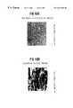
Referring to FIGS. 3 and 4, heated portions of the second comparison specimens W(B) are shown which have metallographic structures on each surface of the heated portions. In FIG. 3, the heated portion of the second comparison specimen is heated by the electron beam to a temperature of 1100° C. while the heated portion of the second comparison specimen is heated by the electron beam to a temperature of 240° C. in FIG.4. At any rate, serious disruptions take place on the heated portions of the second comparison specimens W(B).
Referring to FIGS.5(A) and (B), heated portions of the first specimen W(1) are shown which have metallographic structures on surfaces of the heated portions. In FIGS.5(A) and (B), the heated portion of the first specimen is heated by the electron beam to a temperature of 140° C. and 980° C., respectively. As is readily understood from FIGS.5(A) and (B), grain boundaries are left on the surfaces of the heated portions and no disruption takes place on the surfaces of the heated portions. In addition, it is noted in FIGS.5(A) and (B) that the heated portions are not molten by the heating of the electron beam.
Alternatively, second specimens have been prepared by the use of the apparatus illustrated in FIG.1. In this event, thefirst gas nozzle 18 had a single injection hole of 7.5 mm in diameter. The other conditions were kept unchanged. Under the circumstances, a tungsten layer was deposited on themolybdenum plate 14 at a deposition rate of 200 micron meters/hour.
After the deposition of the tungsten layer, themolybdenum plate 14 was mechanically or chemically removed from the tungsten plate and, as a result, specimens were formed which were composed of the tungsten layer alone and which will be called second specimens W(2) or second CVD-W specimens. Like in the first specimens, metallographic structures of the second specimens have been measured by the use of a microscope and have been found to be columnar structures.
In FIG.6(A), the first specimen W(1) is composed of fine equi-axed crystal grains stacked along a growth direction of the crystals. On the other hand, FIG.6(B) shows that the second specimen W(2) is composed of columnar crystal grains extended along the growth direction of the crystals.
Although the second specimen has a metal-lographic structure different from that of the first specimen, as shown in FIGS.6(A) and6(B), it has been found out that the second specimen is similar in included gases, impurities, and erosion to the first specimen.
Furthermore, a bending test has been carried out as regards the first specimen W(1), the second specimen W(2), and the first comparison specimen W(A).
Referring to FIG. 7, the results of the bending test are shown by curves W(1), W(2), and W(A) which correspond to the specimens W(1), W(2), and W(A), respectively, and which represent relationships between temperatures (K) and flexural strength (GPa). In FIG. 7, it is noted that white circles, triangles, and squares show that breakage occurs at a bending angle less than 10 degrees while black circles, triangles, and squares show that no breakage occurs even at a bending angle greater than 50 degrees.
From FIG. 7, it is apparent that flexural strength is not reduced in both of the first and the second specimens W(1) and W(2) even when a temperature is raised up.
In addition, average thermal expansion coefficients and thermal conductivities have been measured as regards the first and the second specimens W(1) and W(2) and the second comparison specimens W(B). On measuring the average thermal expansion coefficients, the thermal expansion coefficients have been measured at each temperature range between 20° C. and each of 100 through 900° C. to obtain measured results within the respective temperature ranges. The measured results have been averaged within each temperature range. On the other hand, a laser flash method has been used to measure the thermal conductivities. The measured results are shown in Tables 3 and 4.
| TABLE 3 |
| Average Thermal Expansion Coefficients From 20° C. |
| (10−6/° C.) |
| (° C.) | W(1) | W(2) | W(B) | ||
| 20-100 | 4.1 | 4.3 | 3.9 | ||
| 20-200 | 4.4 | 4.4 | 4.4 | ||
| 20-300 | 4.5 | 4.5 | 4.5 | ||
| 20-400 | 4.6 | 4.5 | 4.5 | ||
| 20-500 | 4.6 | 4.5 | 4.6 | ||
| 20-600 | 4.7 | 4.5 | 4.7 | ||
| 20-700 | 4.7 | 4.5 | 4.9 | ||
| 20-800 | 4.8 | 4.4 | 5.0 | ||
| 20-900 | 4.9 | 4.5 | 5.1 | ||
In FIG. 1, it is possible to reduce a total amount of gas components to 2 ppm or less by controlling an amount of the WF6gas supplied to theplate 14. Moreover, the total amount of the gas components have been found to be reduced to 1.5 ppm or less by changing various conditions mentioned in connection with FIG.1.
In addition, it is possible to reduce a total amount of metal impurities to 2 ppm or less and to consequently obtain the tungsten layer which has a purity of tungsten very close to 99.99999%. Thus, the tungsten layer deposited by the CVD method has an extremely high purity as compared with the tungsten layer formed by the powder metallurgical method and can therefore drastically reduce low vapor pressure components which remains by a powder metallurgical method.
As shown in FIG. 7, the first specimens have the fine equi-axed grain structure and exhibit the flexural strength which becomes strong as the temperature is raised up. In this event, the grain size may fall within a range between 0.05 and 5.00 micron meters.
Referring to FIG. 8, comparison of erosion has been made between the first specimen W(1) and the graphite specimen (Gr). To this end, a relationship between energy density (J/cm2) and an erosion depth or depth of erosion is shown in connection with W(1), and Gr in FIG.8. Specifically, the electron beam of high energy density heated each specimen to measure the erosion depth on each specimen. As shown in FIG. 8, the erosion depth in the first specimen W(1) is nearly one third of the erosion depth in the graphite specimen Gr at 100° C. or so and one sixth of the erosion depth in the latter at 1000° C. From this fact, it is readily understood that the tungsten layer deposited by the CVD method is excellent in thermal stability and withstands erosion, as compared with the plasma facing member of tungsten manufactured by the powder metallurgical method. This shows that the tungsten layer according to this invention would be very desirable as the plasma facing member in nuclear fusion reactors or the like. Especially, when the tungsten layer is several millimeters thick or more, the thermal stability and the like are remarkably improved in the plasma facing member according to this invention. Practically, when the tungsten layer deposited by the CVD method has a thickness less than 500 micron meters, it has been confirmed that the tungsten layer is weak against the thermal shock and is not suitable for the plasma facing member.
While this invention has thus far been described in conjunction with a few embodiments thereof, it will be readily possible for those skilled in the art to put this invention into practice in various other manners. For example, the substrate of the plasma facing member may be formed by tungsten, Cu alloy, stainless steel, Nb alloy, v alloy, etc.
Claims (2)
1. A method of forming a plasma facing surface on a substrate formed of predetermined material by chemical vapor deposition in a reaction chamber, said method comprising:
uniformly depositing, on the substrate, a tungsten layer at a deposition rate of 360 μm/hour to a thickness of 2.5 mm by heating the substrate to a predetermined temperature, rotating the substrate at a predetermined speed, supplying a hydrogen gas and a WF6gas into the reaction chamber to form a mixture of the hydrogen gas and the WF6gas having a ratio of the WF6gas to the hydrogen gas of 1:5 to maintain a pressure of the reaction chamber at 1.3 kPa, and causing the mixed hydrogen and WF6to flow at a predetermined flow rate.
2. A method as claimed in claim1, wherein the predetermined material of the substrate is one material selected from a group consisting of molybdenum, tungsten, Cu alloy, stainless steel, Nb alloy, and V alloy.
Priority Applications (1)
| Application Number | Priority Date | Filing Date | Title |
|---|---|---|---|
| US09/836,225US6610375B2 (en) | 1994-02-15 | 2001-04-18 | Plasma facing components of nuclear fusion reactors employing tungsten materials |
Applications Claiming Priority (2)
| Application Number | Priority Date | Filing Date | Title |
|---|---|---|---|
| JP6-039256 | 1994-02-15 | ||
| JP6039256AJP2844304B2 (en) | 1994-02-15 | 1994-02-15 | Plasma facing material |
Related Child Applications (1)
| Application Number | Title | Priority Date | Filing Date |
|---|---|---|---|
| US09/836,225DivisionUS6610375B2 (en) | 1994-02-15 | 2001-04-18 | Plasma facing components of nuclear fusion reactors employing tungsten materials |
Publications (1)
| Publication Number | Publication Date |
|---|---|
| US6261648B1true US6261648B1 (en) | 2001-07-17 |
Family
ID=12548066
Family Applications (2)
| Application Number | Title | Priority Date | Filing Date |
|---|---|---|---|
| US08/388,819Expired - Fee RelatedUS6261648B1 (en) | 1994-02-15 | 1995-02-15 | Plasma facing components of nuclear fusion reactors employing tungsten materials |
| US09/836,225Expired - Fee RelatedUS6610375B2 (en) | 1994-02-15 | 2001-04-18 | Plasma facing components of nuclear fusion reactors employing tungsten materials |
Family Applications After (1)
| Application Number | Title | Priority Date | Filing Date |
|---|---|---|---|
| US09/836,225Expired - Fee RelatedUS6610375B2 (en) | 1994-02-15 | 2001-04-18 | Plasma facing components of nuclear fusion reactors employing tungsten materials |
Country Status (2)
| Country | Link |
|---|---|
| US (2) | US6261648B1 (en) |
| JP (1) | JP2844304B2 (en) |
Cited By (296)
| Publication number | Priority date | Publication date | Assignee | Title |
|---|---|---|---|---|
| US20030180445A1 (en)* | 2002-03-21 | 2003-09-25 | Industrial Scientific Corporation | Method for forming a catalytic bead sensor |
| US20100291767A1 (en)* | 2009-05-18 | 2010-11-18 | Renesas Technology Corp. | Manufacturing method of semiconductor device |
| US20110101534A1 (en)* | 2009-11-04 | 2011-05-05 | International Business Machines Corporation | Automated short length wire shape strapping and methods of fabricting the same |
| US10844486B2 (en) | 2009-04-06 | 2020-11-24 | Asm Ip Holding B.V. | Semiconductor processing reactor and components thereof |
| US10847366B2 (en) | 2018-11-16 | 2020-11-24 | Asm Ip Holding B.V. | Methods for depositing a transition metal chalcogenide film on a substrate by a cyclical deposition process |
| US10844484B2 (en) | 2017-09-22 | 2020-11-24 | Asm Ip Holding B.V. | Apparatus for dispensing a vapor phase reactant to a reaction chamber and related methods |
| US10851456B2 (en) | 2016-04-21 | 2020-12-01 | Asm Ip Holding B.V. | Deposition of metal borides |
| US10858737B2 (en) | 2014-07-28 | 2020-12-08 | Asm Ip Holding B.V. | Showerhead assembly and components thereof |
| US10867788B2 (en) | 2016-12-28 | 2020-12-15 | Asm Ip Holding B.V. | Method of forming a structure on a substrate |
| US10867786B2 (en) | 2018-03-30 | 2020-12-15 | Asm Ip Holding B.V. | Substrate processing method |
| US10883175B2 (en) | 2018-08-09 | 2021-01-05 | Asm Ip Holding B.V. | Vertical furnace for processing substrates and a liner for use therein |
| US10886123B2 (en) | 2017-06-02 | 2021-01-05 | Asm Ip Holding B.V. | Methods for forming low temperature semiconductor layers and related semiconductor device structures |
| US10892156B2 (en) | 2017-05-08 | 2021-01-12 | Asm Ip Holding B.V. | Methods for forming a silicon nitride film on a substrate and related semiconductor device structures |
| US10910262B2 (en) | 2017-11-16 | 2021-02-02 | Asm Ip Holding B.V. | Method of selectively depositing a capping layer structure on a semiconductor device structure |
| US10914004B2 (en) | 2018-06-29 | 2021-02-09 | Asm Ip Holding B.V. | Thin-film deposition method and manufacturing method of semiconductor device |
| US10923344B2 (en) | 2017-10-30 | 2021-02-16 | Asm Ip Holding B.V. | Methods for forming a semiconductor structure and related semiconductor structures |
| US10928731B2 (en) | 2017-09-21 | 2021-02-23 | Asm Ip Holding B.V. | Method of sequential infiltration synthesis treatment of infiltrateable material and structures and devices formed using same |
| US10934619B2 (en) | 2016-11-15 | 2021-03-02 | Asm Ip Holding B.V. | Gas supply unit and substrate processing apparatus including the gas supply unit |
| US10943771B2 (en) | 2016-10-26 | 2021-03-09 | Asm Ip Holding B.V. | Methods for thermally calibrating reaction chambers |
| US10941490B2 (en) | 2014-10-07 | 2021-03-09 | Asm Ip Holding B.V. | Multiple temperature range susceptor, assembly, reactor and system including the susceptor, and methods of using the same |
| US10950432B2 (en) | 2017-04-25 | 2021-03-16 | Asm Ip Holding B.V. | Method of depositing thin film and method of manufacturing semiconductor device |
| USD913980S1 (en) | 2018-02-01 | 2021-03-23 | Asm Ip Holding B.V. | Gas supply plate for semiconductor manufacturing apparatus |
| US10975470B2 (en) | 2018-02-23 | 2021-04-13 | Asm Ip Holding B.V. | Apparatus for detecting or monitoring for a chemical precursor in a high temperature environment |
| US11004977B2 (en) | 2017-07-19 | 2021-05-11 | Asm Ip Holding B.V. | Method for depositing a group IV semiconductor and related semiconductor device structures |
| US11001925B2 (en) | 2016-12-19 | 2021-05-11 | Asm Ip Holding B.V. | Substrate processing apparatus |
| US11018002B2 (en) | 2017-07-19 | 2021-05-25 | Asm Ip Holding B.V. | Method for selectively depositing a Group IV semiconductor and related semiconductor device structures |
| US11015245B2 (en) | 2014-03-19 | 2021-05-25 | Asm Ip Holding B.V. | Gas-phase reactor and system having exhaust plenum and components thereof |
| US11018047B2 (en) | 2018-01-25 | 2021-05-25 | Asm Ip Holding B.V. | Hybrid lift pin |
| US11024523B2 (en) | 2018-09-11 | 2021-06-01 | Asm Ip Holding B.V. | Substrate processing apparatus and method |
| US11022879B2 (en) | 2017-11-24 | 2021-06-01 | Asm Ip Holding B.V. | Method of forming an enhanced unexposed photoresist layer |
| US11031242B2 (en) | 2018-11-07 | 2021-06-08 | Asm Ip Holding B.V. | Methods for depositing a boron doped silicon germanium film |
| USD922229S1 (en) | 2019-06-05 | 2021-06-15 | Asm Ip Holding B.V. | Device for controlling a temperature of a gas supply unit |
| US11049751B2 (en) | 2018-09-14 | 2021-06-29 | Asm Ip Holding B.V. | Cassette supply system to store and handle cassettes and processing apparatus equipped therewith |
| US11053591B2 (en) | 2018-08-06 | 2021-07-06 | Asm Ip Holding B.V. | Multi-port gas injection system and reactor system including same |
| US11056567B2 (en) | 2018-05-11 | 2021-07-06 | Asm Ip Holding B.V. | Method of forming a doped metal carbide film on a substrate and related semiconductor device structures |
| US11056344B2 (en) | 2017-08-30 | 2021-07-06 | Asm Ip Holding B.V. | Layer forming method |
| US11069510B2 (en) | 2017-08-30 | 2021-07-20 | Asm Ip Holding B.V. | Substrate processing apparatus |
| US11081345B2 (en) | 2018-02-06 | 2021-08-03 | Asm Ip Holding B.V. | Method of post-deposition treatment for silicon oxide film |
| US11088002B2 (en) | 2018-03-29 | 2021-08-10 | Asm Ip Holding B.V. | Substrate rack and a substrate processing system and method |
| US11087997B2 (en) | 2018-10-31 | 2021-08-10 | Asm Ip Holding B.V. | Substrate processing apparatus for processing substrates |
| US11094546B2 (en) | 2017-10-05 | 2021-08-17 | Asm Ip Holding B.V. | Method for selectively depositing a metallic film on a substrate |
| US11094582B2 (en) | 2016-07-08 | 2021-08-17 | Asm Ip Holding B.V. | Selective deposition method to form air gaps |
| US11101370B2 (en) | 2016-05-02 | 2021-08-24 | Asm Ip Holding B.V. | Method of forming a germanium oxynitride film |
| US11107676B2 (en) | 2016-07-28 | 2021-08-31 | Asm Ip Holding B.V. | Method and apparatus for filling a gap |
| US11114294B2 (en) | 2019-03-08 | 2021-09-07 | Asm Ip Holding B.V. | Structure including SiOC layer and method of forming same |
| US11114283B2 (en)* | 2018-03-16 | 2021-09-07 | Asm Ip Holding B.V. | Reactor, system including the reactor, and methods of manufacturing and using same |
| USD930782S1 (en) | 2019-08-22 | 2021-09-14 | Asm Ip Holding B.V. | Gas distributor |
| US11127617B2 (en) | 2017-11-27 | 2021-09-21 | Asm Ip Holding B.V. | Storage device for storing wafer cassettes for use with a batch furnace |
| US11127589B2 (en) | 2019-02-01 | 2021-09-21 | Asm Ip Holding B.V. | Method of topology-selective film formation of silicon oxide |
| USD931978S1 (en) | 2019-06-27 | 2021-09-28 | Asm Ip Holding B.V. | Showerhead vacuum transport |
| US11139308B2 (en) | 2015-12-29 | 2021-10-05 | Asm Ip Holding B.V. | Atomic layer deposition of III-V compounds to form V-NAND devices |
| US11139191B2 (en) | 2017-08-09 | 2021-10-05 | Asm Ip Holding B.V. | Storage apparatus for storing cassettes for substrates and processing apparatus equipped therewith |
| US11158513B2 (en) | 2018-12-13 | 2021-10-26 | Asm Ip Holding B.V. | Methods for forming a rhenium-containing film on a substrate by a cyclical deposition process and related semiconductor device structures |
| US11164955B2 (en) | 2017-07-18 | 2021-11-02 | Asm Ip Holding B.V. | Methods for forming a semiconductor device structure and related semiconductor device structures |
| US11171025B2 (en) | 2019-01-22 | 2021-11-09 | Asm Ip Holding B.V. | Substrate processing device |
| US11168395B2 (en) | 2018-06-29 | 2021-11-09 | Asm Ip Holding B.V. | Temperature-controlled flange and reactor system including same |
| USD935572S1 (en) | 2019-05-24 | 2021-11-09 | Asm Ip Holding B.V. | Gas channel plate |
| US11205585B2 (en) | 2016-07-28 | 2021-12-21 | Asm Ip Holding B.V. | Substrate processing apparatus and method of operating the same |
| US11217444B2 (en) | 2018-11-30 | 2022-01-04 | Asm Ip Holding B.V. | Method for forming an ultraviolet radiation responsive metal oxide-containing film |
| USD940837S1 (en) | 2019-08-22 | 2022-01-11 | Asm Ip Holding B.V. | Electrode |
| US11222772B2 (en) | 2016-12-14 | 2022-01-11 | Asm Ip Holding B.V. | Substrate processing apparatus |
| US11227782B2 (en) | 2019-07-31 | 2022-01-18 | Asm Ip Holding B.V. | Vertical batch furnace assembly |
| US11227789B2 (en) | 2019-02-20 | 2022-01-18 | Asm Ip Holding B.V. | Method and apparatus for filling a recess formed within a substrate surface |
| US11230766B2 (en) | 2018-03-29 | 2022-01-25 | Asm Ip Holding B.V. | Substrate processing apparatus and method |
| US11233133B2 (en) | 2015-10-21 | 2022-01-25 | Asm Ip Holding B.V. | NbMC layers |
| US11232963B2 (en) | 2018-10-03 | 2022-01-25 | Asm Ip Holding B.V. | Substrate processing apparatus and method |
| US11242598B2 (en) | 2015-06-26 | 2022-02-08 | Asm Ip Holding B.V. | Structures including metal carbide material, devices including the structures, and methods of forming same |
| US11251035B2 (en) | 2016-12-22 | 2022-02-15 | Asm Ip Holding B.V. | Method of forming a structure on a substrate |
| US11251068B2 (en) | 2018-10-19 | 2022-02-15 | Asm Ip Holding B.V. | Substrate processing apparatus and substrate processing method |
| US11251040B2 (en) | 2019-02-20 | 2022-02-15 | Asm Ip Holding B.V. | Cyclical deposition method including treatment step and apparatus for same |
| USD944946S1 (en) | 2019-06-14 | 2022-03-01 | Asm Ip Holding B.V. | Shower plate |
| US11270899B2 (en) | 2018-06-04 | 2022-03-08 | Asm Ip Holding B.V. | Wafer handling chamber with moisture reduction |
| US11274369B2 (en) | 2018-09-11 | 2022-03-15 | Asm Ip Holding B.V. | Thin film deposition method |
| US11282698B2 (en) | 2019-07-19 | 2022-03-22 | Asm Ip Holding B.V. | Method of forming topology-controlled amorphous carbon polymer film |
| US11286562B2 (en) | 2018-06-08 | 2022-03-29 | Asm Ip Holding B.V. | Gas-phase chemical reactor and method of using same |
| US11286558B2 (en) | 2019-08-23 | 2022-03-29 | Asm Ip Holding B.V. | Methods for depositing a molybdenum nitride film on a surface of a substrate by a cyclical deposition process and related semiconductor device structures including a molybdenum nitride film |
| US11289326B2 (en) | 2019-05-07 | 2022-03-29 | Asm Ip Holding B.V. | Method for reforming amorphous carbon polymer film |
| US11296189B2 (en) | 2018-06-21 | 2022-04-05 | Asm Ip Holding B.V. | Method for depositing a phosphorus doped silicon arsenide film and related semiconductor device structures |
| US11295980B2 (en) | 2017-08-30 | 2022-04-05 | Asm Ip Holding B.V. | Methods for depositing a molybdenum metal film over a dielectric surface of a substrate by a cyclical deposition process and related semiconductor device structures |
| USD947913S1 (en) | 2019-05-17 | 2022-04-05 | Asm Ip Holding B.V. | Susceptor shaft |
| USD948463S1 (en) | 2018-10-24 | 2022-04-12 | Asm Ip Holding B.V. | Susceptor for semiconductor substrate supporting apparatus |
| USD949319S1 (en) | 2019-08-22 | 2022-04-19 | Asm Ip Holding B.V. | Exhaust duct |
| US11306395B2 (en) | 2017-06-28 | 2022-04-19 | Asm Ip Holding B.V. | Methods for depositing a transition metal nitride film on a substrate by atomic layer deposition and related deposition apparatus |
| US11315794B2 (en) | 2019-10-21 | 2022-04-26 | Asm Ip Holding B.V. | Apparatus and methods for selectively etching films |
| US11342216B2 (en) | 2019-02-20 | 2022-05-24 | Asm Ip Holding B.V. | Cyclical deposition method and apparatus for filling a recess formed within a substrate surface |
| US11339476B2 (en) | 2019-10-08 | 2022-05-24 | Asm Ip Holding B.V. | Substrate processing device having connection plates, substrate processing method |
| US11345999B2 (en) | 2019-06-06 | 2022-05-31 | Asm Ip Holding B.V. | Method of using a gas-phase reactor system including analyzing exhausted gas |
| US11355338B2 (en) | 2019-05-10 | 2022-06-07 | Asm Ip Holding B.V. | Method of depositing material onto a surface and structure formed according to the method |
| US11361990B2 (en) | 2018-05-28 | 2022-06-14 | Asm Ip Holding B.V. | Substrate processing method and device manufactured by using the same |
| US11374112B2 (en) | 2017-07-19 | 2022-06-28 | Asm Ip Holding B.V. | Method for depositing a group IV semiconductor and related semiconductor device structures |
| US11378337B2 (en) | 2019-03-28 | 2022-07-05 | Asm Ip Holding B.V. | Door opener and substrate processing apparatus provided therewith |
| US11387106B2 (en) | 2018-02-14 | 2022-07-12 | Asm Ip Holding B.V. | Method for depositing a ruthenium-containing film on a substrate by a cyclical deposition process |
| US11387120B2 (en) | 2017-09-28 | 2022-07-12 | Asm Ip Holding B.V. | Chemical dispensing apparatus and methods for dispensing a chemical to a reaction chamber |
| US11390950B2 (en) | 2017-01-10 | 2022-07-19 | Asm Ip Holding B.V. | Reactor system and method to reduce residue buildup during a film deposition process |
| US11393690B2 (en) | 2018-01-19 | 2022-07-19 | Asm Ip Holding B.V. | Deposition method |
| US11390945B2 (en) | 2019-07-03 | 2022-07-19 | Asm Ip Holding B.V. | Temperature control assembly for substrate processing apparatus and method of using same |
| US11390946B2 (en) | 2019-01-17 | 2022-07-19 | Asm Ip Holding B.V. | Methods of forming a transition metal containing film on a substrate by a cyclical deposition process |
| US11398382B2 (en) | 2018-03-27 | 2022-07-26 | Asm Ip Holding B.V. | Method of forming an electrode on a substrate and a semiconductor device structure including an electrode |
| US11401605B2 (en) | 2019-11-26 | 2022-08-02 | Asm Ip Holding B.V. | Substrate processing apparatus |
| US11411088B2 (en) | 2018-11-16 | 2022-08-09 | Asm Ip Holding B.V. | Methods for forming a metal silicate film on a substrate in a reaction chamber and related semiconductor device structures |
| US11410851B2 (en) | 2017-02-15 | 2022-08-09 | Asm Ip Holding B.V. | Methods for forming a metallic film on a substrate by cyclical deposition and related semiconductor device structures |
| US11414760B2 (en) | 2018-10-08 | 2022-08-16 | Asm Ip Holding B.V. | Substrate support unit, thin film deposition apparatus including the same, and substrate processing apparatus including the same |
| US11417545B2 (en) | 2017-08-08 | 2022-08-16 | Asm Ip Holding B.V. | Radiation shield |
| US11424119B2 (en) | 2019-03-08 | 2022-08-23 | Asm Ip Holding B.V. | Method for selective deposition of silicon nitride layer and structure including selectively-deposited silicon nitride layer |
| US11430674B2 (en) | 2018-08-22 | 2022-08-30 | Asm Ip Holding B.V. | Sensor array, apparatus for dispensing a vapor phase reactant to a reaction chamber and related methods |
| US11430640B2 (en) | 2019-07-30 | 2022-08-30 | Asm Ip Holding B.V. | Substrate processing apparatus |
| US11437241B2 (en) | 2020-04-08 | 2022-09-06 | Asm Ip Holding B.V. | Apparatus and methods for selectively etching silicon oxide films |
| US11443926B2 (en) | 2019-07-30 | 2022-09-13 | Asm Ip Holding B.V. | Substrate processing apparatus |
| US11447861B2 (en) | 2016-12-15 | 2022-09-20 | Asm Ip Holding B.V. | Sequential infiltration synthesis apparatus and a method of forming a patterned structure |
| US11447864B2 (en) | 2019-04-19 | 2022-09-20 | Asm Ip Holding B.V. | Layer forming method and apparatus |
| USD965044S1 (en) | 2019-08-19 | 2022-09-27 | Asm Ip Holding B.V. | Susceptor shaft |
| US11453943B2 (en) | 2016-05-25 | 2022-09-27 | Asm Ip Holding B.V. | Method for forming carbon-containing silicon/metal oxide or nitride film by ALD using silicon precursor and hydrocarbon precursor |
| USD965524S1 (en) | 2019-08-19 | 2022-10-04 | Asm Ip Holding B.V. | Susceptor support |
| US11469098B2 (en) | 2018-05-08 | 2022-10-11 | Asm Ip Holding B.V. | Methods for depositing an oxide film on a substrate by a cyclical deposition process and related device structures |
| US11476109B2 (en) | 2019-06-11 | 2022-10-18 | Asm Ip Holding B.V. | Method of forming an electronic structure using reforming gas, system for performing the method, and structure formed using the method |
| US11473195B2 (en) | 2018-03-01 | 2022-10-18 | Asm Ip Holding B.V. | Semiconductor processing apparatus and a method for processing a substrate |
| US11482418B2 (en) | 2018-02-20 | 2022-10-25 | Asm Ip Holding B.V. | Substrate processing method and apparatus |
| US11482533B2 (en) | 2019-02-20 | 2022-10-25 | Asm Ip Holding B.V. | Apparatus and methods for plug fill deposition in 3-D NAND applications |
| US11482412B2 (en) | 2018-01-19 | 2022-10-25 | Asm Ip Holding B.V. | Method for depositing a gap-fill layer by plasma-assisted deposition |
| US11488854B2 (en) | 2020-03-11 | 2022-11-01 | Asm Ip Holding B.V. | Substrate handling device with adjustable joints |
| US11488819B2 (en) | 2018-12-04 | 2022-11-01 | Asm Ip Holding B.V. | Method of cleaning substrate processing apparatus |
| US11495459B2 (en) | 2019-09-04 | 2022-11-08 | Asm Ip Holding B.V. | Methods for selective deposition using a sacrificial capping layer |
| US11492703B2 (en) | 2018-06-27 | 2022-11-08 | Asm Ip Holding B.V. | Cyclic deposition methods for forming metal-containing material and films and structures including the metal-containing material |
| US11499222B2 (en) | 2018-06-27 | 2022-11-15 | Asm Ip Holding B.V. | Cyclic deposition methods for forming metal-containing material and films and structures including the metal-containing material |
| US11499226B2 (en) | 2018-11-02 | 2022-11-15 | Asm Ip Holding B.V. | Substrate supporting unit and a substrate processing device including the same |
| US11501973B2 (en) | 2018-01-16 | 2022-11-15 | Asm Ip Holding B.V. | Method for depositing a material film on a substrate within a reaction chamber by a cyclical deposition process and related device structures |
| US11501968B2 (en) | 2019-11-15 | 2022-11-15 | Asm Ip Holding B.V. | Method for providing a semiconductor device with silicon filled gaps |
| US11501956B2 (en) | 2012-10-12 | 2022-11-15 | Asm Ip Holding B.V. | Semiconductor reaction chamber showerhead |
| US11515187B2 (en) | 2020-05-01 | 2022-11-29 | Asm Ip Holding B.V. | Fast FOUP swapping with a FOUP handler |
| US11515188B2 (en) | 2019-05-16 | 2022-11-29 | Asm Ip Holding B.V. | Wafer boat handling device, vertical batch furnace and method |
| US11521851B2 (en) | 2020-02-03 | 2022-12-06 | Asm Ip Holding B.V. | Method of forming structures including a vanadium or indium layer |
| US11527400B2 (en) | 2019-08-23 | 2022-12-13 | Asm Ip Holding B.V. | Method for depositing silicon oxide film having improved quality by peald using bis(diethylamino)silane |
| US11527403B2 (en) | 2019-12-19 | 2022-12-13 | Asm Ip Holding B.V. | Methods for filling a gap feature on a substrate surface and related semiconductor structures |
| US11530876B2 (en) | 2020-04-24 | 2022-12-20 | Asm Ip Holding B.V. | Vertical batch furnace assembly comprising a cooling gas supply |
| US11530483B2 (en) | 2018-06-21 | 2022-12-20 | Asm Ip Holding B.V. | Substrate processing system |
| US11532757B2 (en) | 2016-10-27 | 2022-12-20 | Asm Ip Holding B.V. | Deposition of charge trapping layers |
| US11551925B2 (en) | 2019-04-01 | 2023-01-10 | Asm Ip Holding B.V. | Method for manufacturing a semiconductor device |
| US11551912B2 (en) | 2020-01-20 | 2023-01-10 | Asm Ip Holding B.V. | Method of forming thin film and method of modifying surface of thin film |
| US11557474B2 (en) | 2019-07-29 | 2023-01-17 | Asm Ip Holding B.V. | Methods for selective deposition utilizing n-type dopants and/or alternative dopants to achieve high dopant incorporation |
| USD975665S1 (en) | 2019-05-17 | 2023-01-17 | Asm Ip Holding B.V. | Susceptor shaft |
| US11562901B2 (en) | 2019-09-25 | 2023-01-24 | Asm Ip Holding B.V. | Substrate processing method |
| US11572620B2 (en) | 2018-11-06 | 2023-02-07 | Asm Ip Holding B.V. | Methods for selectively depositing an amorphous silicon film on a substrate |
| US11581186B2 (en) | 2016-12-15 | 2023-02-14 | Asm Ip Holding B.V. | Sequential infiltration synthesis apparatus |
| US11587815B2 (en) | 2019-07-31 | 2023-02-21 | Asm Ip Holding B.V. | Vertical batch furnace assembly |
| US11587821B2 (en) | 2017-08-08 | 2023-02-21 | Asm Ip Holding B.V. | Substrate lift mechanism and reactor including same |
| US11587814B2 (en) | 2019-07-31 | 2023-02-21 | Asm Ip Holding B.V. | Vertical batch furnace assembly |
| US11594600B2 (en) | 2019-11-05 | 2023-02-28 | Asm Ip Holding B.V. | Structures with doped semiconductor layers and methods and systems for forming same |
| USD979506S1 (en) | 2019-08-22 | 2023-02-28 | Asm Ip Holding B.V. | Insulator |
| US11594450B2 (en) | 2019-08-22 | 2023-02-28 | Asm Ip Holding B.V. | Method for forming a structure with a hole |
| USD980813S1 (en) | 2021-05-11 | 2023-03-14 | Asm Ip Holding B.V. | Gas flow control plate for substrate processing apparatus |
| US11605528B2 (en) | 2019-07-09 | 2023-03-14 | Asm Ip Holding B.V. | Plasma device using coaxial waveguide, and substrate treatment method |
| USD980814S1 (en) | 2021-05-11 | 2023-03-14 | Asm Ip Holding B.V. | Gas distributor for substrate processing apparatus |
| US11610774B2 (en) | 2019-10-02 | 2023-03-21 | Asm Ip Holding B.V. | Methods for forming a topographically selective silicon oxide film by a cyclical plasma-enhanced deposition process |
| US11610775B2 (en) | 2016-07-28 | 2023-03-21 | Asm Ip Holding B.V. | Method and apparatus for filling a gap |
| USD981973S1 (en) | 2021-05-11 | 2023-03-28 | Asm Ip Holding B.V. | Reactor wall for substrate processing apparatus |
| US11615970B2 (en) | 2019-07-17 | 2023-03-28 | Asm Ip Holding B.V. | Radical assist ignition plasma system and method |
| US11626308B2 (en) | 2020-05-13 | 2023-04-11 | Asm Ip Holding B.V. | Laser alignment fixture for a reactor system |
| US11626316B2 (en) | 2019-11-20 | 2023-04-11 | Asm Ip Holding B.V. | Method of depositing carbon-containing material on a surface of a substrate, structure formed using the method, and system for forming the structure |
| US11629407B2 (en) | 2019-02-22 | 2023-04-18 | Asm Ip Holding B.V. | Substrate processing apparatus and method for processing substrates |
| US11629406B2 (en) | 2018-03-09 | 2023-04-18 | Asm Ip Holding B.V. | Semiconductor processing apparatus comprising one or more pyrometers for measuring a temperature of a substrate during transfer of the substrate |
| US11637011B2 (en) | 2019-10-16 | 2023-04-25 | Asm Ip Holding B.V. | Method of topology-selective film formation of silicon oxide |
| US11637014B2 (en) | 2019-10-17 | 2023-04-25 | Asm Ip Holding B.V. | Methods for selective deposition of doped semiconductor material |
| US11639548B2 (en) | 2019-08-21 | 2023-05-02 | Asm Ip Holding B.V. | Film-forming material mixed-gas forming device and film forming device |
| US11639811B2 (en) | 2017-11-27 | 2023-05-02 | Asm Ip Holding B.V. | Apparatus including a clean mini environment |
| US11646197B2 (en) | 2018-07-03 | 2023-05-09 | Asm Ip Holding B.V. | Method for depositing silicon-free carbon-containing film as gap-fill layer by pulse plasma-assisted deposition |
| US11644758B2 (en) | 2020-07-17 | 2023-05-09 | Asm Ip Holding B.V. | Structures and methods for use in photolithography |
| US11646204B2 (en) | 2020-06-24 | 2023-05-09 | Asm Ip Holding B.V. | Method for forming a layer provided with silicon |
| US11643724B2 (en) | 2019-07-18 | 2023-05-09 | Asm Ip Holding B.V. | Method of forming structures using a neutral beam |
| US11646205B2 (en) | 2019-10-29 | 2023-05-09 | Asm Ip Holding B.V. | Methods of selectively forming n-type doped material on a surface, systems for selectively forming n-type doped material, and structures formed using same |
| US11646184B2 (en) | 2019-11-29 | 2023-05-09 | Asm Ip Holding B.V. | Substrate processing apparatus |
| US11649546B2 (en) | 2016-07-08 | 2023-05-16 | Asm Ip Holding B.V. | Organic reactants for atomic layer deposition |
| US11658029B2 (en) | 2018-12-14 | 2023-05-23 | Asm Ip Holding B.V. | Method of forming a device structure using selective deposition of gallium nitride and system for same |
| US11658030B2 (en) | 2017-03-29 | 2023-05-23 | Asm Ip Holding B.V. | Method for forming doped metal oxide films on a substrate by cyclical deposition and related semiconductor device structures |
| US11658035B2 (en) | 2020-06-30 | 2023-05-23 | Asm Ip Holding B.V. | Substrate processing method |
| US11664199B2 (en) | 2018-10-19 | 2023-05-30 | Asm Ip Holding B.V. | Substrate processing apparatus and substrate processing method |
| US11664245B2 (en) | 2019-07-16 | 2023-05-30 | Asm Ip Holding B.V. | Substrate processing device |
| US11664267B2 (en) | 2019-07-10 | 2023-05-30 | Asm Ip Holding B.V. | Substrate support assembly and substrate processing device including the same |
| US11674220B2 (en) | 2020-07-20 | 2023-06-13 | Asm Ip Holding B.V. | Method for depositing molybdenum layers using an underlayer |
| US11676812B2 (en) | 2016-02-19 | 2023-06-13 | Asm Ip Holding B.V. | Method for forming silicon nitride film selectively on top/bottom portions |
| US11680839B2 (en) | 2019-08-05 | 2023-06-20 | Asm Ip Holding B.V. | Liquid level sensor for a chemical source vessel |
| US11688603B2 (en) | 2019-07-17 | 2023-06-27 | Asm Ip Holding B.V. | Methods of forming silicon germanium structures |
| US11685991B2 (en) | 2018-02-14 | 2023-06-27 | Asm Ip Holding B.V. | Method for depositing a ruthenium-containing film on a substrate by a cyclical deposition process |
| USD990441S1 (en) | 2021-09-07 | 2023-06-27 | Asm Ip Holding B.V. | Gas flow control plate |
| USD990534S1 (en) | 2020-09-11 | 2023-06-27 | Asm Ip Holding B.V. | Weighted lift pin |
| US11705333B2 (en) | 2020-05-21 | 2023-07-18 | Asm Ip Holding B.V. | Structures including multiple carbon layers and methods of forming and using same |
| US11718913B2 (en) | 2018-06-04 | 2023-08-08 | Asm Ip Holding B.V. | Gas distribution system and reactor system including same |
| US11725280B2 (en) | 2020-08-26 | 2023-08-15 | Asm Ip Holding B.V. | Method for forming metal silicon oxide and metal silicon oxynitride layers |
| US11725277B2 (en) | 2011-07-20 | 2023-08-15 | Asm Ip Holding B.V. | Pressure transmitter for a semiconductor processing environment |
| US11735422B2 (en) | 2019-10-10 | 2023-08-22 | Asm Ip Holding B.V. | Method of forming a photoresist underlayer and structure including same |
| US20230268084A1 (en)* | 2021-03-15 | 2023-08-24 | Dalian University Of Technology | Simulation method for electron temperature evolution caused by east tokamak radiofrequency wave |
| US11742189B2 (en) | 2015-03-12 | 2023-08-29 | Asm Ip Holding B.V. | Multi-zone reactor, system including the reactor, and method of using the same |
| US11742198B2 (en) | 2019-03-08 | 2023-08-29 | Asm Ip Holding B.V. | Structure including SiOCN layer and method of forming same |
| US11767589B2 (en) | 2020-05-29 | 2023-09-26 | Asm Ip Holding B.V. | Substrate processing device |
| US11769682B2 (en) | 2017-08-09 | 2023-09-26 | Asm Ip Holding B.V. | Storage apparatus for storing cassettes for substrates and processing apparatus equipped therewith |
| US11776846B2 (en) | 2020-02-07 | 2023-10-03 | Asm Ip Holding B.V. | Methods for depositing gap filling fluids and related systems and devices |
| US11781243B2 (en) | 2020-02-17 | 2023-10-10 | Asm Ip Holding B.V. | Method for depositing low temperature phosphorous-doped silicon |
| US11781221B2 (en) | 2019-05-07 | 2023-10-10 | Asm Ip Holding B.V. | Chemical source vessel with dip tube |
| US11802338B2 (en) | 2017-07-26 | 2023-10-31 | Asm Ip Holding B.V. | Chemical treatment, deposition and/or infiltration apparatus and method for using the same |
| US11804364B2 (en) | 2020-05-19 | 2023-10-31 | Asm Ip Holding B.V. | Substrate processing apparatus |
| US11810788B2 (en) | 2016-11-01 | 2023-11-07 | Asm Ip Holding B.V. | Methods for forming a transition metal niobium nitride film on a substrate by atomic layer deposition and related semiconductor device structures |
| US11814747B2 (en) | 2019-04-24 | 2023-11-14 | Asm Ip Holding B.V. | Gas-phase reactor system-with a reaction chamber, a solid precursor source vessel, a gas distribution system, and a flange assembly |
| US11823866B2 (en) | 2020-04-02 | 2023-11-21 | Asm Ip Holding B.V. | Thin film forming method |
| US11821078B2 (en) | 2020-04-15 | 2023-11-21 | Asm Ip Holding B.V. | Method for forming precoat film and method for forming silicon-containing film |
| US11823876B2 (en) | 2019-09-05 | 2023-11-21 | Asm Ip Holding B.V. | Substrate processing apparatus |
| US11828707B2 (en) | 2020-02-04 | 2023-11-28 | Asm Ip Holding B.V. | Method and apparatus for transmittance measurements of large articles |
| US11827981B2 (en) | 2020-10-14 | 2023-11-28 | Asm Ip Holding B.V. | Method of depositing material on stepped structure |
| US11830730B2 (en) | 2017-08-29 | 2023-11-28 | Asm Ip Holding B.V. | Layer forming method and apparatus |
| US11830738B2 (en) | 2020-04-03 | 2023-11-28 | Asm Ip Holding B.V. | Method for forming barrier layer and method for manufacturing semiconductor device |
| US11840761B2 (en) | 2019-12-04 | 2023-12-12 | Asm Ip Holding B.V. | Substrate processing apparatus |
| US11848200B2 (en) | 2017-05-08 | 2023-12-19 | Asm Ip Holding B.V. | Methods for selectively forming a silicon nitride film on a substrate and related semiconductor device structures |
| US11873557B2 (en) | 2020-10-22 | 2024-01-16 | Asm Ip Holding B.V. | Method of depositing vanadium metal |
| US11876356B2 (en) | 2020-03-11 | 2024-01-16 | Asm Ip Holding B.V. | Lockout tagout assembly and system and method of using same |
| US11885013B2 (en) | 2019-12-17 | 2024-01-30 | Asm Ip Holding B.V. | Method of forming vanadium nitride layer and structure including the vanadium nitride layer |
| US11885020B2 (en) | 2020-12-22 | 2024-01-30 | Asm Ip Holding B.V. | Transition metal deposition method |
| US11887857B2 (en) | 2020-04-24 | 2024-01-30 | Asm Ip Holding B.V. | Methods and systems for depositing a layer comprising vanadium, nitrogen, and a further element |
| US11885023B2 (en) | 2018-10-01 | 2024-01-30 | Asm Ip Holding B.V. | Substrate retaining apparatus, system including the apparatus, and method of using same |
| USD1012873S1 (en) | 2020-09-24 | 2024-01-30 | Asm Ip Holding B.V. | Electrode for semiconductor processing apparatus |
| US11891696B2 (en) | 2020-11-30 | 2024-02-06 | Asm Ip Holding B.V. | Injector configured for arrangement within a reaction chamber of a substrate processing apparatus |
| US11898243B2 (en) | 2020-04-24 | 2024-02-13 | Asm Ip Holding B.V. | Method of forming vanadium nitride-containing layer |
| US11901179B2 (en) | 2020-10-28 | 2024-02-13 | Asm Ip Holding B.V. | Method and device for depositing silicon onto substrates |
| US11915929B2 (en) | 2019-11-26 | 2024-02-27 | Asm Ip Holding B.V. | Methods for selectively forming a target film on a substrate comprising a first dielectric surface and a second metallic surface |
| US11923190B2 (en) | 2018-07-03 | 2024-03-05 | Asm Ip Holding B.V. | Method for depositing silicon-free carbon-containing film as gap-fill layer by pulse plasma-assisted deposition |
| US11923181B2 (en) | 2019-11-29 | 2024-03-05 | Asm Ip Holding B.V. | Substrate processing apparatus for minimizing the effect of a filling gas during substrate processing |
| US11929251B2 (en) | 2019-12-02 | 2024-03-12 | Asm Ip Holding B.V. | Substrate processing apparatus having electrostatic chuck and substrate processing method |
| US11946137B2 (en) | 2020-12-16 | 2024-04-02 | Asm Ip Holding B.V. | Runout and wobble measurement fixtures |
| US11959168B2 (en) | 2020-04-29 | 2024-04-16 | Asm Ip Holding B.V. | Solid source precursor vessel |
| US11961741B2 (en) | 2020-03-12 | 2024-04-16 | Asm Ip Holding B.V. | Method for fabricating layer structure having target topological profile |
| USD1023959S1 (en) | 2021-05-11 | 2024-04-23 | Asm Ip Holding B.V. | Electrode for substrate processing apparatus |
| US11967488B2 (en) | 2013-02-01 | 2024-04-23 | Asm Ip Holding B.V. | Method for treatment of deposition reactor |
| US11976359B2 (en) | 2020-01-06 | 2024-05-07 | Asm Ip Holding B.V. | Gas supply assembly, components thereof, and reactor system including same |
| US11987881B2 (en) | 2020-05-22 | 2024-05-21 | Asm Ip Holding B.V. | Apparatus for depositing thin films using hydrogen peroxide |
| US11986868B2 (en) | 2020-02-28 | 2024-05-21 | Asm Ip Holding B.V. | System dedicated for parts cleaning |
| US11993847B2 (en) | 2020-01-08 | 2024-05-28 | Asm Ip Holding B.V. | Injector |
| US11993843B2 (en) | 2017-08-31 | 2024-05-28 | Asm Ip Holding B.V. | Substrate processing apparatus |
| US11996292B2 (en) | 2019-10-25 | 2024-05-28 | Asm Ip Holding B.V. | Methods for filling a gap feature on a substrate surface and related semiconductor structures |
| US11996289B2 (en) | 2020-04-16 | 2024-05-28 | Asm Ip Holding B.V. | Methods of forming structures including silicon germanium and silicon layers, devices formed using the methods, and systems for performing the methods |
| US11996309B2 (en) | 2019-05-16 | 2024-05-28 | Asm Ip Holding B.V. | Wafer boat handling device, vertical batch furnace and method |
| US12009241B2 (en) | 2019-10-14 | 2024-06-11 | Asm Ip Holding B.V. | Vertical batch furnace assembly with detector to detect cassette |
| US12006572B2 (en) | 2019-10-08 | 2024-06-11 | Asm Ip Holding B.V. | Reactor system including a gas distribution assembly for use with activated species and method of using same |
| US12009224B2 (en) | 2020-09-29 | 2024-06-11 | Asm Ip Holding B.V. | Apparatus and method for etching metal nitrides |
| US12020934B2 (en) | 2020-07-08 | 2024-06-25 | Asm Ip Holding B.V. | Substrate processing method |
| US12027365B2 (en) | 2020-11-24 | 2024-07-02 | Asm Ip Holding B.V. | Methods for filling a gap and related systems and devices |
| US12025484B2 (en) | 2018-05-08 | 2024-07-02 | Asm Ip Holding B.V. | Thin film forming method |
| US12033885B2 (en) | 2020-01-06 | 2024-07-09 | Asm Ip Holding B.V. | Channeled lift pin |
| US12040199B2 (en) | 2018-11-28 | 2024-07-16 | Asm Ip Holding B.V. | Substrate processing apparatus for processing substrates |
| US12040200B2 (en) | 2017-06-20 | 2024-07-16 | Asm Ip Holding B.V. | Semiconductor processing apparatus and methods for calibrating a semiconductor processing apparatus |
| US12040177B2 (en) | 2020-08-18 | 2024-07-16 | Asm Ip Holding B.V. | Methods for forming a laminate film by cyclical plasma-enhanced deposition processes |
| US12051567B2 (en) | 2020-10-07 | 2024-07-30 | Asm Ip Holding B.V. | Gas supply unit and substrate processing apparatus including gas supply unit |
| US12051602B2 (en) | 2020-05-04 | 2024-07-30 | Asm Ip Holding B.V. | Substrate processing system for processing substrates with an electronics module located behind a door in a front wall of the substrate processing system |
| US12057314B2 (en) | 2020-05-15 | 2024-08-06 | Asm Ip Holding B.V. | Methods for silicon germanium uniformity control using multiple precursors |
| US12074022B2 (en) | 2020-08-27 | 2024-08-27 | Asm Ip Holding B.V. | Method and system for forming patterned structures using multiple patterning process |
| US12087586B2 (en) | 2020-04-15 | 2024-09-10 | Asm Ip Holding B.V. | Method of forming chromium nitride layer and structure including the chromium nitride layer |
| US12107005B2 (en) | 2020-10-06 | 2024-10-01 | Asm Ip Holding B.V. | Deposition method and an apparatus for depositing a silicon-containing material |
| US12106944B2 (en) | 2020-06-02 | 2024-10-01 | Asm Ip Holding B.V. | Rotating substrate support |
| US12112940B2 (en) | 2019-07-19 | 2024-10-08 | Asm Ip Holding B.V. | Method of forming topology-controlled amorphous carbon polymer film |
| US12125700B2 (en) | 2020-01-16 | 2024-10-22 | Asm Ip Holding B.V. | Method of forming high aspect ratio features |
| US12129545B2 (en) | 2020-12-22 | 2024-10-29 | Asm Ip Holding B.V. | Precursor capsule, a vessel and a method |
| US12131885B2 (en) | 2020-12-22 | 2024-10-29 | Asm Ip Holding B.V. | Plasma treatment device having matching box |
| US12148609B2 (en) | 2020-09-16 | 2024-11-19 | Asm Ip Holding B.V. | Silicon oxide deposition method |
| US12154824B2 (en) | 2020-08-14 | 2024-11-26 | Asm Ip Holding B.V. | Substrate processing method |
| US12159788B2 (en) | 2020-12-14 | 2024-12-03 | Asm Ip Holding B.V. | Method of forming structures for threshold voltage control |
| US12169361B2 (en) | 2019-07-30 | 2024-12-17 | Asm Ip Holding B.V. | Substrate processing apparatus and method |
| US12173402B2 (en) | 2018-02-15 | 2024-12-24 | Asm Ip Holding B.V. | Method of forming a transition metal containing film on a substrate by a cyclical deposition process, a method for supplying a transition metal halide compound to a reaction chamber, and related vapor deposition apparatus |
| US12173404B2 (en) | 2020-03-17 | 2024-12-24 | Asm Ip Holding B.V. | Method of depositing epitaxial material, structure formed using the method, and system for performing the method |
| US12195852B2 (en) | 2020-11-23 | 2025-01-14 | Asm Ip Holding B.V. | Substrate processing apparatus with an injector |
| US12203166B2 (en) | 2020-05-07 | 2025-01-21 | Asm Ip Holding B.V. | Apparatus and methods for performing an in-situ etch of reaction chambers with fluorine-based radicals |
| US12209308B2 (en) | 2020-11-12 | 2025-01-28 | Asm Ip Holding B.V. | Reactor and related methods |
| US12211742B2 (en) | 2020-09-10 | 2025-01-28 | Asm Ip Holding B.V. | Methods for depositing gap filling fluid |
| US12218000B2 (en) | 2020-09-25 | 2025-02-04 | Asm Ip Holding B.V. | Semiconductor processing method |
| US12217954B2 (en) | 2020-08-25 | 2025-02-04 | Asm Ip Holding B.V. | Method of cleaning a surface |
| US12218269B2 (en) | 2020-02-13 | 2025-02-04 | Asm Ip Holding B.V. | Substrate processing apparatus including light receiving device and calibration method of light receiving device |
| US12217946B2 (en) | 2020-10-15 | 2025-02-04 | Asm Ip Holding B.V. | Method of manufacturing semiconductor device, and substrate treatment apparatus using ether-CAT |
| USD1060598S1 (en) | 2021-12-03 | 2025-02-04 | Asm Ip Holding B.V. | Split showerhead cover |
| US12221357B2 (en) | 2020-04-24 | 2025-02-11 | Asm Ip Holding B.V. | Methods and apparatus for stabilizing vanadium compounds |
| US12230531B2 (en) | 2018-04-09 | 2025-02-18 | Asm Ip Holding B.V. | Substrate supporting apparatus, substrate processing apparatus including the same, and substrate processing method |
| US12241158B2 (en) | 2020-07-20 | 2025-03-04 | Asm Ip Holding B.V. | Method for forming structures including transition metal layers |
| US12243757B2 (en) | 2020-05-21 | 2025-03-04 | Asm Ip Holding B.V. | Flange and apparatus for processing substrates |
| US12243747B2 (en) | 2020-04-24 | 2025-03-04 | Asm Ip Holding B.V. | Methods of forming structures including vanadium boride and vanadium phosphide layers |
| US12240760B2 (en) | 2016-03-18 | 2025-03-04 | Asm Ip Holding B.V. | Aligned carbon nanotubes |
| US12243742B2 (en) | 2020-04-21 | 2025-03-04 | Asm Ip Holding B.V. | Method for processing a substrate |
| US12247286B2 (en) | 2019-08-09 | 2025-03-11 | Asm Ip Holding B.V. | Heater assembly including cooling apparatus and method of using same |
| US12252785B2 (en) | 2019-06-10 | 2025-03-18 | Asm Ip Holding B.V. | Method for cleaning quartz epitaxial chambers |
| US12255053B2 (en) | 2020-12-10 | 2025-03-18 | Asm Ip Holding B.V. | Methods and systems for depositing a layer |
| US12266524B2 (en) | 2020-06-16 | 2025-04-01 | Asm Ip Holding B.V. | Method for depositing boron containing silicon germanium layers |
| US12272527B2 (en) | 2018-05-09 | 2025-04-08 | Asm Ip Holding B.V. | Apparatus for use with hydrogen radicals and method of using same |
| US12276023B2 (en) | 2017-08-04 | 2025-04-15 | Asm Ip Holding B.V. | Showerhead assembly for distributing a gas within a reaction chamber |
| US12278129B2 (en) | 2020-03-04 | 2025-04-15 | Asm Ip Holding B.V. | Alignment fixture for a reactor system |
| US12288710B2 (en) | 2020-12-18 | 2025-04-29 | Asm Ip Holding B.V. | Wafer processing apparatus with a rotatable table |
| US12322591B2 (en) | 2020-07-27 | 2025-06-03 | Asm Ip Holding B.V. | Thin film deposition process |
| US12378665B2 (en) | 2018-10-26 | 2025-08-05 | Asm Ip Holding B.V. | High temperature coatings for a preclean and etch apparatus and related methods |
| US12406846B2 (en) | 2020-05-26 | 2025-09-02 | Asm Ip Holding B.V. | Method for depositing boron and gallium containing silicon germanium layers |
| US12410515B2 (en) | 2020-01-29 | 2025-09-09 | Asm Ip Holding B.V. | Contaminant trap system for a reactor system |
| US12428726B2 (en) | 2019-10-08 | 2025-09-30 | Asm Ip Holding B.V. | Gas injection system and reactor system including same |
| US12431354B2 (en) | 2020-07-01 | 2025-09-30 | Asm Ip Holding B.V. | Silicon nitride and silicon oxide deposition methods using fluorine inhibitor |
| US12431334B2 (en) | 2020-02-13 | 2025-09-30 | Asm Ip Holding B.V. | Gas distribution assembly |
| US12444599B2 (en) | 2021-12-08 | 2025-10-14 | Asm Ip Holding B.V. | Method for forming an ultraviolet radiation responsive metal oxide-containing film |
Families Citing this family (10)
| Publication number | Priority date | Publication date | Assignee | Title |
|---|---|---|---|---|
| US7094614B2 (en)* | 2001-01-16 | 2006-08-22 | International Business Machines Corporation | In-situ monitoring of chemical vapor deposition process by mass spectrometry |
| US8090857B2 (en) | 2003-11-24 | 2012-01-03 | Qualcomm Atheros, Inc. | Medium access control layer that encapsulates data from a plurality of received data units into a plurality of independently transmittable blocks |
| US8175190B2 (en) | 2005-07-27 | 2012-05-08 | Qualcomm Atheros, Inc. | Managing spectra of modulated signals in a communication network |
| US7900817B2 (en)* | 2006-01-26 | 2011-03-08 | Ricoh Company, Ltd. | Techniques for introducing devices to device families with paper receipt |
| TW200811310A (en)* | 2006-08-23 | 2008-03-01 | Kinik Co | Apparatus for chemical gas phase thin film sedimentation |
| EP2073243B1 (en)* | 2007-12-21 | 2018-10-03 | Applied Materials, Inc. | Linear electron source, evaporator using linear electron source, and applications of electron sources |
| US9633751B2 (en) | 2011-04-01 | 2017-04-25 | The Boeing Company | Liquid lithium first walls for electromagnetic control of plasmas in fusion power reactor environments |
| CN103352222B (en)* | 2013-06-24 | 2016-03-02 | 核工业西南物理研究院 | A kind of preparation method of the carbon-base tungsten coating for tokamak device |
| CN104120406B (en)* | 2014-07-02 | 2016-06-15 | 厦门润晶光电集团有限公司 | The tungsten crucible trimming device of long crystal furnace use and method |
| CN111415761B (en)* | 2019-01-07 | 2022-03-11 | 新奥科技发展有限公司 | Plasma-oriented part and fusion device |
Citations (19)
| Publication number | Priority date | Publication date | Assignee | Title |
|---|---|---|---|---|
| US3663273A (en)* | 1970-11-16 | 1972-05-16 | Ladd Res Ind | Tilting variable speed rotary shadower |
| US3784824A (en)* | 1970-01-23 | 1974-01-08 | Philips Corp | Tritium target with compensated sputtering |
| US4145250A (en)* | 1976-02-26 | 1979-03-20 | General Atomic Company | In situ regeneration of the first wall of a deuterium-tritium fusion device |
| US4234622A (en)* | 1979-04-11 | 1980-11-18 | The United States Of American As Represented By The Secretary Of The Army | Vacuum deposition method |
| US4298804A (en)* | 1978-10-13 | 1981-11-03 | U.S. Philips Corporation | Neutron generator having a target |
| JPS6098385A (en)* | 1983-11-04 | 1985-06-01 | 株式会社東芝 | Limiter device in fusion device |
| US4555275A (en)* | 1984-10-19 | 1985-11-26 | Grumman Aerospace Corporation | Hydrogen permeation protection for metals |
| US4619807A (en)* | 1981-07-01 | 1986-10-28 | Max-Planck-Gesellschaft Zur Foerderung Der Wisenschaften E.V. | Heat shield |
| US4721595A (en)* | 1985-01-29 | 1988-01-26 | The United States Of America As Represented By The United States Department Of Energy | First wall for polarized fusion reactors |
| US4935194A (en)* | 1988-04-19 | 1990-06-19 | U.S. Philips Corporation | High-flux neutron generator comprising a long-life target |
| USH984H (en)* | 1983-12-21 | 1991-11-05 | The United States Of America As Represented By The United States Department Of Energy | Self-pumping impurity control |
| US5081069A (en)* | 1989-12-26 | 1992-01-14 | Texas Instruments Incorporated | Method for depositing a Tio2 layer using a periodic and simultaneous tilting and rotating platform motion |
| JPH04105096A (en)* | 1990-08-24 | 1992-04-07 | Toshiba Corp | fusion reactor |
| US5182075A (en)* | 1989-05-24 | 1993-01-26 | Hitachi, Ltd. | Nuclear fusion reactor |
| US5260106A (en)* | 1990-08-03 | 1993-11-09 | Fujitsu Limited | Method for forming diamond films by plasma jet CVD |
| US5342660A (en)* | 1991-05-10 | 1994-08-30 | Celestech, Inc. | Method for plasma jet deposition |
| US5390217A (en)* | 1988-04-28 | 1995-02-14 | Mitsubishi Jukogyo Kabushiki Kaisha | Carbon fiber-reinforced carbon composite materials processes for their production, and first walls of nuclear fusion reactors employing them |
| US5410574A (en)* | 1992-12-28 | 1995-04-25 | Kabushiki Kaisha Toshiba | Internal component of fusion reactor |
| US5509472A (en)* | 1991-11-14 | 1996-04-23 | Kabushiki Kaisha Toshiba | Heat-resisting plate having a cooling structure and method of manufacturing it |
- 1994
- 1994-02-15JPJP6039256Apatent/JP2844304B2/ennot_activeExpired - Fee Related
- 1995
- 1995-02-15USUS08/388,819patent/US6261648B1/ennot_activeExpired - Fee Related
- 2001
- 2001-04-18USUS09/836,225patent/US6610375B2/ennot_activeExpired - Fee Related
Patent Citations (19)
| Publication number | Priority date | Publication date | Assignee | Title |
|---|---|---|---|---|
| US3784824A (en)* | 1970-01-23 | 1974-01-08 | Philips Corp | Tritium target with compensated sputtering |
| US3663273A (en)* | 1970-11-16 | 1972-05-16 | Ladd Res Ind | Tilting variable speed rotary shadower |
| US4145250A (en)* | 1976-02-26 | 1979-03-20 | General Atomic Company | In situ regeneration of the first wall of a deuterium-tritium fusion device |
| US4298804A (en)* | 1978-10-13 | 1981-11-03 | U.S. Philips Corporation | Neutron generator having a target |
| US4234622A (en)* | 1979-04-11 | 1980-11-18 | The United States Of American As Represented By The Secretary Of The Army | Vacuum deposition method |
| US4619807A (en)* | 1981-07-01 | 1986-10-28 | Max-Planck-Gesellschaft Zur Foerderung Der Wisenschaften E.V. | Heat shield |
| JPS6098385A (en)* | 1983-11-04 | 1985-06-01 | 株式会社東芝 | Limiter device in fusion device |
| USH984H (en)* | 1983-12-21 | 1991-11-05 | The United States Of America As Represented By The United States Department Of Energy | Self-pumping impurity control |
| US4555275A (en)* | 1984-10-19 | 1985-11-26 | Grumman Aerospace Corporation | Hydrogen permeation protection for metals |
| US4721595A (en)* | 1985-01-29 | 1988-01-26 | The United States Of America As Represented By The United States Department Of Energy | First wall for polarized fusion reactors |
| US4935194A (en)* | 1988-04-19 | 1990-06-19 | U.S. Philips Corporation | High-flux neutron generator comprising a long-life target |
| US5390217A (en)* | 1988-04-28 | 1995-02-14 | Mitsubishi Jukogyo Kabushiki Kaisha | Carbon fiber-reinforced carbon composite materials processes for their production, and first walls of nuclear fusion reactors employing them |
| US5182075A (en)* | 1989-05-24 | 1993-01-26 | Hitachi, Ltd. | Nuclear fusion reactor |
| US5081069A (en)* | 1989-12-26 | 1992-01-14 | Texas Instruments Incorporated | Method for depositing a Tio2 layer using a periodic and simultaneous tilting and rotating platform motion |
| US5260106A (en)* | 1990-08-03 | 1993-11-09 | Fujitsu Limited | Method for forming diamond films by plasma jet CVD |
| JPH04105096A (en)* | 1990-08-24 | 1992-04-07 | Toshiba Corp | fusion reactor |
| US5342660A (en)* | 1991-05-10 | 1994-08-30 | Celestech, Inc. | Method for plasma jet deposition |
| US5509472A (en)* | 1991-11-14 | 1996-04-23 | Kabushiki Kaisha Toshiba | Heat-resisting plate having a cooling structure and method of manufacturing it |
| US5410574A (en)* | 1992-12-28 | 1995-04-25 | Kabushiki Kaisha Toshiba | Internal component of fusion reactor |
Non-Patent Citations (12)
| Title |
|---|
| ANL/EPP/TM-174, May 1983, Brooks et al (III), pp. 1-18.* |
| ANL/FPP/TM-175, Jun. 1983, Brooks et al (IV), pp. 1-25.* |
| ANL/FPP/TM-188, May 1984, Brooks et al(II) pp. 43-66.* |
| ANL/FPP/TM-246, Mar. 1990, Mattas, pp. 1-46.* |
| Conf: 9th Symp. on Engineering Problems of Fusion Research. Chicago, IL., Oct. 1981, pp. 1597-1600, Morgan et al.* |
| GA-A17266, Nov. 1983, Trester et al. (identified as pp. 1-6).* |
| INTOR report "zero phase", IAEA, vienna,(1980) chapter XI, pp. 324-329.* |
| Nuclear Fusion, vol. 20, No. 10, (1980), pp. 1335-1340, clausing.* |
| Nuclear Technology/Fusion, vol. 4, Jul. 1983, pp. 33-45, Brooks.* |
| Proc. 4th European Conf. on Chemical Vapour Depositions, (1983) pp. 340-349, "CVD Coatings in Fusion Reactor Technology", Brossa.* |
| T. Kuroda et al., "ITER Plasma Facing Components", International Atomic Energy Agency, Vienna 1991, in ITER Documentation Series No. 30, pp. 18, 22, 33, 40. |
| Thin Films Science and Technology s7, Tihn Films by Chemical Vapour Deposition, Elsevier, Amsterdam, (1990), by C.E. Morosanu, pp. 31-70.* |
Cited By (356)
| Publication number | Priority date | Publication date | Assignee | Title |
|---|---|---|---|---|
| US20030180445A1 (en)* | 2002-03-21 | 2003-09-25 | Industrial Scientific Corporation | Method for forming a catalytic bead sensor |
| US10844486B2 (en) | 2009-04-06 | 2020-11-24 | Asm Ip Holding B.V. | Semiconductor processing reactor and components thereof |
| US9177813B2 (en)* | 2009-05-18 | 2015-11-03 | Renesas Electronics Corporation | Manufacturing method of semiconductor device |
| US20100291767A1 (en)* | 2009-05-18 | 2010-11-18 | Renesas Technology Corp. | Manufacturing method of semiconductor device |
| US20110101534A1 (en)* | 2009-11-04 | 2011-05-05 | International Business Machines Corporation | Automated short length wire shape strapping and methods of fabricting the same |
| US11725277B2 (en) | 2011-07-20 | 2023-08-15 | Asm Ip Holding B.V. | Pressure transmitter for a semiconductor processing environment |
| US11501956B2 (en) | 2012-10-12 | 2022-11-15 | Asm Ip Holding B.V. | Semiconductor reaction chamber showerhead |
| US11967488B2 (en) | 2013-02-01 | 2024-04-23 | Asm Ip Holding B.V. | Method for treatment of deposition reactor |
| US11015245B2 (en) | 2014-03-19 | 2021-05-25 | Asm Ip Holding B.V. | Gas-phase reactor and system having exhaust plenum and components thereof |
| US10858737B2 (en) | 2014-07-28 | 2020-12-08 | Asm Ip Holding B.V. | Showerhead assembly and components thereof |
| US11795545B2 (en) | 2014-10-07 | 2023-10-24 | Asm Ip Holding B.V. | Multiple temperature range susceptor, assembly, reactor and system including the susceptor, and methods of using the same |
| US10941490B2 (en) | 2014-10-07 | 2021-03-09 | Asm Ip Holding B.V. | Multiple temperature range susceptor, assembly, reactor and system including the susceptor, and methods of using the same |
| US11742189B2 (en) | 2015-03-12 | 2023-08-29 | Asm Ip Holding B.V. | Multi-zone reactor, system including the reactor, and method of using the same |
| US11242598B2 (en) | 2015-06-26 | 2022-02-08 | Asm Ip Holding B.V. | Structures including metal carbide material, devices including the structures, and methods of forming same |
| US11233133B2 (en) | 2015-10-21 | 2022-01-25 | Asm Ip Holding B.V. | NbMC layers |
| US11956977B2 (en) | 2015-12-29 | 2024-04-09 | Asm Ip Holding B.V. | Atomic layer deposition of III-V compounds to form V-NAND devices |
| US11139308B2 (en) | 2015-12-29 | 2021-10-05 | Asm Ip Holding B.V. | Atomic layer deposition of III-V compounds to form V-NAND devices |
| US11676812B2 (en) | 2016-02-19 | 2023-06-13 | Asm Ip Holding B.V. | Method for forming silicon nitride film selectively on top/bottom portions |
| US12240760B2 (en) | 2016-03-18 | 2025-03-04 | Asm Ip Holding B.V. | Aligned carbon nanotubes |
| US10851456B2 (en) | 2016-04-21 | 2020-12-01 | Asm Ip Holding B.V. | Deposition of metal borides |
| US11101370B2 (en) | 2016-05-02 | 2021-08-24 | Asm Ip Holding B.V. | Method of forming a germanium oxynitride film |
| US11453943B2 (en) | 2016-05-25 | 2022-09-27 | Asm Ip Holding B.V. | Method for forming carbon-containing silicon/metal oxide or nitride film by ALD using silicon precursor and hydrocarbon precursor |
| US11649546B2 (en) | 2016-07-08 | 2023-05-16 | Asm Ip Holding B.V. | Organic reactants for atomic layer deposition |
| US11749562B2 (en) | 2016-07-08 | 2023-09-05 | Asm Ip Holding B.V. | Selective deposition method to form air gaps |
| US11094582B2 (en) | 2016-07-08 | 2021-08-17 | Asm Ip Holding B.V. | Selective deposition method to form air gaps |
| US11107676B2 (en) | 2016-07-28 | 2021-08-31 | Asm Ip Holding B.V. | Method and apparatus for filling a gap |
| US11610775B2 (en) | 2016-07-28 | 2023-03-21 | Asm Ip Holding B.V. | Method and apparatus for filling a gap |
| US11694892B2 (en) | 2016-07-28 | 2023-07-04 | Asm Ip Holding B.V. | Method and apparatus for filling a gap |
| US11205585B2 (en) | 2016-07-28 | 2021-12-21 | Asm Ip Holding B.V. | Substrate processing apparatus and method of operating the same |
| US10943771B2 (en) | 2016-10-26 | 2021-03-09 | Asm Ip Holding B.V. | Methods for thermally calibrating reaction chambers |
| US11532757B2 (en) | 2016-10-27 | 2022-12-20 | Asm Ip Holding B.V. | Deposition of charge trapping layers |
| US11810788B2 (en) | 2016-11-01 | 2023-11-07 | Asm Ip Holding B.V. | Methods for forming a transition metal niobium nitride film on a substrate by atomic layer deposition and related semiconductor device structures |
| US11396702B2 (en) | 2016-11-15 | 2022-07-26 | Asm Ip Holding B.V. | Gas supply unit and substrate processing apparatus including the gas supply unit |
| US10934619B2 (en) | 2016-11-15 | 2021-03-02 | Asm Ip Holding B.V. | Gas supply unit and substrate processing apparatus including the gas supply unit |
| US11222772B2 (en) | 2016-12-14 | 2022-01-11 | Asm Ip Holding B.V. | Substrate processing apparatus |
| US11970766B2 (en) | 2016-12-15 | 2024-04-30 | Asm Ip Holding B.V. | Sequential infiltration synthesis apparatus |
| US11581186B2 (en) | 2016-12-15 | 2023-02-14 | Asm Ip Holding B.V. | Sequential infiltration synthesis apparatus |
| US11447861B2 (en) | 2016-12-15 | 2022-09-20 | Asm Ip Holding B.V. | Sequential infiltration synthesis apparatus and a method of forming a patterned structure |
| US11851755B2 (en) | 2016-12-15 | 2023-12-26 | Asm Ip Holding B.V. | Sequential infiltration synthesis apparatus and a method of forming a patterned structure |
| US12000042B2 (en) | 2016-12-15 | 2024-06-04 | Asm Ip Holding B.V. | Sequential infiltration synthesis apparatus and a method of forming a patterned structure |
| US11001925B2 (en) | 2016-12-19 | 2021-05-11 | Asm Ip Holding B.V. | Substrate processing apparatus |
| US11251035B2 (en) | 2016-12-22 | 2022-02-15 | Asm Ip Holding B.V. | Method of forming a structure on a substrate |
| US10867788B2 (en) | 2016-12-28 | 2020-12-15 | Asm Ip Holding B.V. | Method of forming a structure on a substrate |
| US11390950B2 (en) | 2017-01-10 | 2022-07-19 | Asm Ip Holding B.V. | Reactor system and method to reduce residue buildup during a film deposition process |
| US12043899B2 (en) | 2017-01-10 | 2024-07-23 | Asm Ip Holding B.V. | Reactor system and method to reduce residue buildup during a film deposition process |
| US12106965B2 (en) | 2017-02-15 | 2024-10-01 | Asm Ip Holding B.V. | Methods for forming a metallic film on a substrate by cyclical deposition and related semiconductor device structures |
| US11410851B2 (en) | 2017-02-15 | 2022-08-09 | Asm Ip Holding B.V. | Methods for forming a metallic film on a substrate by cyclical deposition and related semiconductor device structures |
| US11658030B2 (en) | 2017-03-29 | 2023-05-23 | Asm Ip Holding B.V. | Method for forming doped metal oxide films on a substrate by cyclical deposition and related semiconductor device structures |
| US10950432B2 (en) | 2017-04-25 | 2021-03-16 | Asm Ip Holding B.V. | Method of depositing thin film and method of manufacturing semiconductor device |
| US11848200B2 (en) | 2017-05-08 | 2023-12-19 | Asm Ip Holding B.V. | Methods for selectively forming a silicon nitride film on a substrate and related semiconductor device structures |
| US10892156B2 (en) | 2017-05-08 | 2021-01-12 | Asm Ip Holding B.V. | Methods for forming a silicon nitride film on a substrate and related semiconductor device structures |
| US10886123B2 (en) | 2017-06-02 | 2021-01-05 | Asm Ip Holding B.V. | Methods for forming low temperature semiconductor layers and related semiconductor device structures |
| US12040200B2 (en) | 2017-06-20 | 2024-07-16 | Asm Ip Holding B.V. | Semiconductor processing apparatus and methods for calibrating a semiconductor processing apparatus |
| US11976361B2 (en) | 2017-06-28 | 2024-05-07 | Asm Ip Holding B.V. | Methods for depositing a transition metal nitride film on a substrate by atomic layer deposition and related deposition apparatus |
| US11306395B2 (en) | 2017-06-28 | 2022-04-19 | Asm Ip Holding B.V. | Methods for depositing a transition metal nitride film on a substrate by atomic layer deposition and related deposition apparatus |
| US11164955B2 (en) | 2017-07-18 | 2021-11-02 | Asm Ip Holding B.V. | Methods for forming a semiconductor device structure and related semiconductor device structures |
| US11695054B2 (en) | 2017-07-18 | 2023-07-04 | Asm Ip Holding B.V. | Methods for forming a semiconductor device structure and related semiconductor device structures |
| US11004977B2 (en) | 2017-07-19 | 2021-05-11 | Asm Ip Holding B.V. | Method for depositing a group IV semiconductor and related semiconductor device structures |
| US12363960B2 (en) | 2017-07-19 | 2025-07-15 | Asm Ip Holding B.V. | Method for depositing a Group IV semiconductor and related semiconductor device structures |
| US11374112B2 (en) | 2017-07-19 | 2022-06-28 | Asm Ip Holding B.V. | Method for depositing a group IV semiconductor and related semiconductor device structures |
| US11018002B2 (en) | 2017-07-19 | 2021-05-25 | Asm Ip Holding B.V. | Method for selectively depositing a Group IV semiconductor and related semiconductor device structures |
| US11802338B2 (en) | 2017-07-26 | 2023-10-31 | Asm Ip Holding B.V. | Chemical treatment, deposition and/or infiltration apparatus and method for using the same |
| US12276023B2 (en) | 2017-08-04 | 2025-04-15 | Asm Ip Holding B.V. | Showerhead assembly for distributing a gas within a reaction chamber |
| US11587821B2 (en) | 2017-08-08 | 2023-02-21 | Asm Ip Holding B.V. | Substrate lift mechanism and reactor including same |
| US11417545B2 (en) | 2017-08-08 | 2022-08-16 | Asm Ip Holding B.V. | Radiation shield |
| US11139191B2 (en) | 2017-08-09 | 2021-10-05 | Asm Ip Holding B.V. | Storage apparatus for storing cassettes for substrates and processing apparatus equipped therewith |
| US11769682B2 (en) | 2017-08-09 | 2023-09-26 | Asm Ip Holding B.V. | Storage apparatus for storing cassettes for substrates and processing apparatus equipped therewith |
| US11830730B2 (en) | 2017-08-29 | 2023-11-28 | Asm Ip Holding B.V. | Layer forming method and apparatus |
| US11295980B2 (en) | 2017-08-30 | 2022-04-05 | Asm Ip Holding B.V. | Methods for depositing a molybdenum metal film over a dielectric surface of a substrate by a cyclical deposition process and related semiconductor device structures |
| US11069510B2 (en) | 2017-08-30 | 2021-07-20 | Asm Ip Holding B.V. | Substrate processing apparatus |
| US11056344B2 (en) | 2017-08-30 | 2021-07-06 | Asm Ip Holding B.V. | Layer forming method |
| US11581220B2 (en) | 2017-08-30 | 2023-02-14 | Asm Ip Holding B.V. | Methods for depositing a molybdenum metal film over a dielectric surface of a substrate by a cyclical deposition process and related semiconductor device structures |
| US11993843B2 (en) | 2017-08-31 | 2024-05-28 | Asm Ip Holding B.V. | Substrate processing apparatus |
| US10928731B2 (en) | 2017-09-21 | 2021-02-23 | Asm Ip Holding B.V. | Method of sequential infiltration synthesis treatment of infiltrateable material and structures and devices formed using same |
| US10844484B2 (en) | 2017-09-22 | 2020-11-24 | Asm Ip Holding B.V. | Apparatus for dispensing a vapor phase reactant to a reaction chamber and related methods |
| US11387120B2 (en) | 2017-09-28 | 2022-07-12 | Asm Ip Holding B.V. | Chemical dispensing apparatus and methods for dispensing a chemical to a reaction chamber |
| US12033861B2 (en) | 2017-10-05 | 2024-07-09 | Asm Ip Holding B.V. | Method for selectively depositing a metallic film on a substrate |
| US11094546B2 (en) | 2017-10-05 | 2021-08-17 | Asm Ip Holding B.V. | Method for selectively depositing a metallic film on a substrate |
| US10923344B2 (en) | 2017-10-30 | 2021-02-16 | Asm Ip Holding B.V. | Methods for forming a semiconductor structure and related semiconductor structures |
| US12040184B2 (en) | 2017-10-30 | 2024-07-16 | Asm Ip Holding B.V. | Methods for forming a semiconductor structure and related semiconductor structures |
| US10910262B2 (en) | 2017-11-16 | 2021-02-02 | Asm Ip Holding B.V. | Method of selectively depositing a capping layer structure on a semiconductor device structure |
| US11022879B2 (en) | 2017-11-24 | 2021-06-01 | Asm Ip Holding B.V. | Method of forming an enhanced unexposed photoresist layer |
| US11682572B2 (en) | 2017-11-27 | 2023-06-20 | Asm Ip Holdings B.V. | Storage device for storing wafer cassettes for use with a batch furnace |
| US11127617B2 (en) | 2017-11-27 | 2021-09-21 | Asm Ip Holding B.V. | Storage device for storing wafer cassettes for use with a batch furnace |
| US11639811B2 (en) | 2017-11-27 | 2023-05-02 | Asm Ip Holding B.V. | Apparatus including a clean mini environment |
| US11501973B2 (en) | 2018-01-16 | 2022-11-15 | Asm Ip Holding B.V. | Method for depositing a material film on a substrate within a reaction chamber by a cyclical deposition process and related device structures |
| US11482412B2 (en) | 2018-01-19 | 2022-10-25 | Asm Ip Holding B.V. | Method for depositing a gap-fill layer by plasma-assisted deposition |
| US11972944B2 (en) | 2018-01-19 | 2024-04-30 | Asm Ip Holding B.V. | Method for depositing a gap-fill layer by plasma-assisted deposition |
| US12119228B2 (en) | 2018-01-19 | 2024-10-15 | Asm Ip Holding B.V. | Deposition method |
| US11393690B2 (en) | 2018-01-19 | 2022-07-19 | Asm Ip Holding B.V. | Deposition method |
| US11018047B2 (en) | 2018-01-25 | 2021-05-25 | Asm Ip Holding B.V. | Hybrid lift pin |
| USD913980S1 (en) | 2018-02-01 | 2021-03-23 | Asm Ip Holding B.V. | Gas supply plate for semiconductor manufacturing apparatus |
| US11735414B2 (en) | 2018-02-06 | 2023-08-22 | Asm Ip Holding B.V. | Method of post-deposition treatment for silicon oxide film |
| US11081345B2 (en) | 2018-02-06 | 2021-08-03 | Asm Ip Holding B.V. | Method of post-deposition treatment for silicon oxide film |
| US11387106B2 (en) | 2018-02-14 | 2022-07-12 | Asm Ip Holding B.V. | Method for depositing a ruthenium-containing film on a substrate by a cyclical deposition process |
| US11685991B2 (en) | 2018-02-14 | 2023-06-27 | Asm Ip Holding B.V. | Method for depositing a ruthenium-containing film on a substrate by a cyclical deposition process |
| US12173402B2 (en) | 2018-02-15 | 2024-12-24 | Asm Ip Holding B.V. | Method of forming a transition metal containing film on a substrate by a cyclical deposition process, a method for supplying a transition metal halide compound to a reaction chamber, and related vapor deposition apparatus |
| US11482418B2 (en) | 2018-02-20 | 2022-10-25 | Asm Ip Holding B.V. | Substrate processing method and apparatus |
| US10975470B2 (en) | 2018-02-23 | 2021-04-13 | Asm Ip Holding B.V. | Apparatus for detecting or monitoring for a chemical precursor in a high temperature environment |
| US11939673B2 (en) | 2018-02-23 | 2024-03-26 | Asm Ip Holding B.V. | Apparatus for detecting or monitoring for a chemical precursor in a high temperature environment |
| US11473195B2 (en) | 2018-03-01 | 2022-10-18 | Asm Ip Holding B.V. | Semiconductor processing apparatus and a method for processing a substrate |
| US11629406B2 (en) | 2018-03-09 | 2023-04-18 | Asm Ip Holding B.V. | Semiconductor processing apparatus comprising one or more pyrometers for measuring a temperature of a substrate during transfer of the substrate |
| US11114283B2 (en)* | 2018-03-16 | 2021-09-07 | Asm Ip Holding B.V. | Reactor, system including the reactor, and methods of manufacturing and using same |
| US12020938B2 (en) | 2018-03-27 | 2024-06-25 | Asm Ip Holding B.V. | Method of forming an electrode on a substrate and a semiconductor device structure including an electrode |
| US11398382B2 (en) | 2018-03-27 | 2022-07-26 | Asm Ip Holding B.V. | Method of forming an electrode on a substrate and a semiconductor device structure including an electrode |
| US11088002B2 (en) | 2018-03-29 | 2021-08-10 | Asm Ip Holding B.V. | Substrate rack and a substrate processing system and method |
| US11230766B2 (en) | 2018-03-29 | 2022-01-25 | Asm Ip Holding B.V. | Substrate processing apparatus and method |
| US10867786B2 (en) | 2018-03-30 | 2020-12-15 | Asm Ip Holding B.V. | Substrate processing method |
| US12230531B2 (en) | 2018-04-09 | 2025-02-18 | Asm Ip Holding B.V. | Substrate supporting apparatus, substrate processing apparatus including the same, and substrate processing method |
| US12025484B2 (en) | 2018-05-08 | 2024-07-02 | Asm Ip Holding B.V. | Thin film forming method |
| US11469098B2 (en) | 2018-05-08 | 2022-10-11 | Asm Ip Holding B.V. | Methods for depositing an oxide film on a substrate by a cyclical deposition process and related device structures |
| US12272527B2 (en) | 2018-05-09 | 2025-04-08 | Asm Ip Holding B.V. | Apparatus for use with hydrogen radicals and method of using same |
| US11056567B2 (en) | 2018-05-11 | 2021-07-06 | Asm Ip Holding B.V. | Method of forming a doped metal carbide film on a substrate and related semiconductor device structures |
| US11908733B2 (en) | 2018-05-28 | 2024-02-20 | Asm Ip Holding B.V. | Substrate processing method and device manufactured by using the same |
| US11361990B2 (en) | 2018-05-28 | 2022-06-14 | Asm Ip Holding B.V. | Substrate processing method and device manufactured by using the same |
| US11837483B2 (en) | 2018-06-04 | 2023-12-05 | Asm Ip Holding B.V. | Wafer handling chamber with moisture reduction |
| US11270899B2 (en) | 2018-06-04 | 2022-03-08 | Asm Ip Holding B.V. | Wafer handling chamber with moisture reduction |
| US11718913B2 (en) | 2018-06-04 | 2023-08-08 | Asm Ip Holding B.V. | Gas distribution system and reactor system including same |
| US11286562B2 (en) | 2018-06-08 | 2022-03-29 | Asm Ip Holding B.V. | Gas-phase chemical reactor and method of using same |
| US11530483B2 (en) | 2018-06-21 | 2022-12-20 | Asm Ip Holding B.V. | Substrate processing system |
| US11296189B2 (en) | 2018-06-21 | 2022-04-05 | Asm Ip Holding B.V. | Method for depositing a phosphorus doped silicon arsenide film and related semiconductor device structures |
| US11814715B2 (en) | 2018-06-27 | 2023-11-14 | Asm Ip Holding B.V. | Cyclic deposition methods for forming metal-containing material and films and structures including the metal-containing material |
| US11952658B2 (en) | 2018-06-27 | 2024-04-09 | Asm Ip Holding B.V. | Cyclic deposition methods for forming metal-containing material and films and structures including the metal-containing material |
| US11492703B2 (en) | 2018-06-27 | 2022-11-08 | Asm Ip Holding B.V. | Cyclic deposition methods for forming metal-containing material and films and structures including the metal-containing material |
| US11499222B2 (en) | 2018-06-27 | 2022-11-15 | Asm Ip Holding B.V. | Cyclic deposition methods for forming metal-containing material and films and structures including the metal-containing material |
| US11168395B2 (en) | 2018-06-29 | 2021-11-09 | Asm Ip Holding B.V. | Temperature-controlled flange and reactor system including same |
| US10914004B2 (en) | 2018-06-29 | 2021-02-09 | Asm Ip Holding B.V. | Thin-film deposition method and manufacturing method of semiconductor device |
| US11923190B2 (en) | 2018-07-03 | 2024-03-05 | Asm Ip Holding B.V. | Method for depositing silicon-free carbon-containing film as gap-fill layer by pulse plasma-assisted deposition |
| US11646197B2 (en) | 2018-07-03 | 2023-05-09 | Asm Ip Holding B.V. | Method for depositing silicon-free carbon-containing film as gap-fill layer by pulse plasma-assisted deposition |
| US11053591B2 (en) | 2018-08-06 | 2021-07-06 | Asm Ip Holding B.V. | Multi-port gas injection system and reactor system including same |
| US10883175B2 (en) | 2018-08-09 | 2021-01-05 | Asm Ip Holding B.V. | Vertical furnace for processing substrates and a liner for use therein |
| US11430674B2 (en) | 2018-08-22 | 2022-08-30 | Asm Ip Holding B.V. | Sensor array, apparatus for dispensing a vapor phase reactant to a reaction chamber and related methods |
| US11024523B2 (en) | 2018-09-11 | 2021-06-01 | Asm Ip Holding B.V. | Substrate processing apparatus and method |
| US11274369B2 (en) | 2018-09-11 | 2022-03-15 | Asm Ip Holding B.V. | Thin film deposition method |
| US11804388B2 (en) | 2018-09-11 | 2023-10-31 | Asm Ip Holding B.V. | Substrate processing apparatus and method |
| US11049751B2 (en) | 2018-09-14 | 2021-06-29 | Asm Ip Holding B.V. | Cassette supply system to store and handle cassettes and processing apparatus equipped therewith |
| US11885023B2 (en) | 2018-10-01 | 2024-01-30 | Asm Ip Holding B.V. | Substrate retaining apparatus, system including the apparatus, and method of using same |
| US11232963B2 (en) | 2018-10-03 | 2022-01-25 | Asm Ip Holding B.V. | Substrate processing apparatus and method |
| US11414760B2 (en) | 2018-10-08 | 2022-08-16 | Asm Ip Holding B.V. | Substrate support unit, thin film deposition apparatus including the same, and substrate processing apparatus including the same |
| US11251068B2 (en) | 2018-10-19 | 2022-02-15 | Asm Ip Holding B.V. | Substrate processing apparatus and substrate processing method |
| US11664199B2 (en) | 2018-10-19 | 2023-05-30 | Asm Ip Holding B.V. | Substrate processing apparatus and substrate processing method |
| USD948463S1 (en) | 2018-10-24 | 2022-04-12 | Asm Ip Holding B.V. | Susceptor for semiconductor substrate supporting apparatus |
| US12378665B2 (en) | 2018-10-26 | 2025-08-05 | Asm Ip Holding B.V. | High temperature coatings for a preclean and etch apparatus and related methods |
| US11087997B2 (en) | 2018-10-31 | 2021-08-10 | Asm Ip Holding B.V. | Substrate processing apparatus for processing substrates |
| US11735445B2 (en) | 2018-10-31 | 2023-08-22 | Asm Ip Holding B.V. | Substrate processing apparatus for processing substrates |
| US11499226B2 (en) | 2018-11-02 | 2022-11-15 | Asm Ip Holding B.V. | Substrate supporting unit and a substrate processing device including the same |
| US11866823B2 (en) | 2018-11-02 | 2024-01-09 | Asm Ip Holding B.V. | Substrate supporting unit and a substrate processing device including the same |
| US11572620B2 (en) | 2018-11-06 | 2023-02-07 | Asm Ip Holding B.V. | Methods for selectively depositing an amorphous silicon film on a substrate |
| US11031242B2 (en) | 2018-11-07 | 2021-06-08 | Asm Ip Holding B.V. | Methods for depositing a boron doped silicon germanium film |
| US11244825B2 (en) | 2018-11-16 | 2022-02-08 | Asm Ip Holding B.V. | Methods for depositing a transition metal chalcogenide film on a substrate by a cyclical deposition process |
| US10847366B2 (en) | 2018-11-16 | 2020-11-24 | Asm Ip Holding B.V. | Methods for depositing a transition metal chalcogenide film on a substrate by a cyclical deposition process |
| US11798999B2 (en) | 2018-11-16 | 2023-10-24 | Asm Ip Holding B.V. | Methods for forming a metal silicate film on a substrate in a reaction chamber and related semiconductor device structures |
| US11411088B2 (en) | 2018-11-16 | 2022-08-09 | Asm Ip Holding B.V. | Methods for forming a metal silicate film on a substrate in a reaction chamber and related semiconductor device structures |
| US12040199B2 (en) | 2018-11-28 | 2024-07-16 | Asm Ip Holding B.V. | Substrate processing apparatus for processing substrates |
| US11217444B2 (en) | 2018-11-30 | 2022-01-04 | Asm Ip Holding B.V. | Method for forming an ultraviolet radiation responsive metal oxide-containing film |
| US11488819B2 (en) | 2018-12-04 | 2022-11-01 | Asm Ip Holding B.V. | Method of cleaning substrate processing apparatus |
| US11158513B2 (en) | 2018-12-13 | 2021-10-26 | Asm Ip Holding B.V. | Methods for forming a rhenium-containing film on a substrate by a cyclical deposition process and related semiconductor device structures |
| US11769670B2 (en) | 2018-12-13 | 2023-09-26 | Asm Ip Holding B.V. | Methods for forming a rhenium-containing film on a substrate by a cyclical deposition process and related semiconductor device structures |
| US11658029B2 (en) | 2018-12-14 | 2023-05-23 | Asm Ip Holding B.V. | Method of forming a device structure using selective deposition of gallium nitride and system for same |
| US11959171B2 (en) | 2019-01-17 | 2024-04-16 | Asm Ip Holding B.V. | Methods of forming a transition metal containing film on a substrate by a cyclical deposition process |
| US11390946B2 (en) | 2019-01-17 | 2022-07-19 | Asm Ip Holding B.V. | Methods of forming a transition metal containing film on a substrate by a cyclical deposition process |
| US11171025B2 (en) | 2019-01-22 | 2021-11-09 | Asm Ip Holding B.V. | Substrate processing device |
| US11127589B2 (en) | 2019-02-01 | 2021-09-21 | Asm Ip Holding B.V. | Method of topology-selective film formation of silicon oxide |
| US11482533B2 (en) | 2019-02-20 | 2022-10-25 | Asm Ip Holding B.V. | Apparatus and methods for plug fill deposition in 3-D NAND applications |
| US11227789B2 (en) | 2019-02-20 | 2022-01-18 | Asm Ip Holding B.V. | Method and apparatus for filling a recess formed within a substrate surface |
| US11342216B2 (en) | 2019-02-20 | 2022-05-24 | Asm Ip Holding B.V. | Cyclical deposition method and apparatus for filling a recess formed within a substrate surface |
| US12176243B2 (en) | 2019-02-20 | 2024-12-24 | Asm Ip Holding B.V. | Method and apparatus for filling a recess formed within a substrate surface |
| US11615980B2 (en) | 2019-02-20 | 2023-03-28 | Asm Ip Holding B.V. | Method and apparatus for filling a recess formed within a substrate surface |
| US11251040B2 (en) | 2019-02-20 | 2022-02-15 | Asm Ip Holding B.V. | Cyclical deposition method including treatment step and apparatus for same |
| US11798834B2 (en) | 2019-02-20 | 2023-10-24 | Asm Ip Holding B.V. | Cyclical deposition method and apparatus for filling a recess formed within a substrate surface |
| US12410522B2 (en) | 2019-02-22 | 2025-09-09 | Asm Ip Holding B.V. | Substrate processing apparatus and method for processing substrates |
| US11629407B2 (en) | 2019-02-22 | 2023-04-18 | Asm Ip Holding B.V. | Substrate processing apparatus and method for processing substrates |
| US11901175B2 (en) | 2019-03-08 | 2024-02-13 | Asm Ip Holding B.V. | Method for selective deposition of silicon nitride layer and structure including selectively-deposited silicon nitride layer |
| US11742198B2 (en) | 2019-03-08 | 2023-08-29 | Asm Ip Holding B.V. | Structure including SiOCN layer and method of forming same |
| US11114294B2 (en) | 2019-03-08 | 2021-09-07 | Asm Ip Holding B.V. | Structure including SiOC layer and method of forming same |
| US11424119B2 (en) | 2019-03-08 | 2022-08-23 | Asm Ip Holding B.V. | Method for selective deposition of silicon nitride layer and structure including selectively-deposited silicon nitride layer |
| US11378337B2 (en) | 2019-03-28 | 2022-07-05 | Asm Ip Holding B.V. | Door opener and substrate processing apparatus provided therewith |
| US11551925B2 (en) | 2019-04-01 | 2023-01-10 | Asm Ip Holding B.V. | Method for manufacturing a semiconductor device |
| US11447864B2 (en) | 2019-04-19 | 2022-09-20 | Asm Ip Holding B.V. | Layer forming method and apparatus |
| US11814747B2 (en) | 2019-04-24 | 2023-11-14 | Asm Ip Holding B.V. | Gas-phase reactor system-with a reaction chamber, a solid precursor source vessel, a gas distribution system, and a flange assembly |
| US11781221B2 (en) | 2019-05-07 | 2023-10-10 | Asm Ip Holding B.V. | Chemical source vessel with dip tube |
| US11289326B2 (en) | 2019-05-07 | 2022-03-29 | Asm Ip Holding B.V. | Method for reforming amorphous carbon polymer film |
| US11355338B2 (en) | 2019-05-10 | 2022-06-07 | Asm Ip Holding B.V. | Method of depositing material onto a surface and structure formed according to the method |
| US11996309B2 (en) | 2019-05-16 | 2024-05-28 | Asm Ip Holding B.V. | Wafer boat handling device, vertical batch furnace and method |
| US11515188B2 (en) | 2019-05-16 | 2022-11-29 | Asm Ip Holding B.V. | Wafer boat handling device, vertical batch furnace and method |
| USD975665S1 (en) | 2019-05-17 | 2023-01-17 | Asm Ip Holding B.V. | Susceptor shaft |
| USD947913S1 (en) | 2019-05-17 | 2022-04-05 | Asm Ip Holding B.V. | Susceptor shaft |
| USD935572S1 (en) | 2019-05-24 | 2021-11-09 | Asm Ip Holding B.V. | Gas channel plate |
| USD922229S1 (en) | 2019-06-05 | 2021-06-15 | Asm Ip Holding B.V. | Device for controlling a temperature of a gas supply unit |
| US11345999B2 (en) | 2019-06-06 | 2022-05-31 | Asm Ip Holding B.V. | Method of using a gas-phase reactor system including analyzing exhausted gas |
| US11453946B2 (en) | 2019-06-06 | 2022-09-27 | Asm Ip Holding B.V. | Gas-phase reactor system including a gas detector |
| US12195855B2 (en) | 2019-06-06 | 2025-01-14 | Asm Ip Holding B.V. | Gas-phase reactor system including a gas detector |
| US12252785B2 (en) | 2019-06-10 | 2025-03-18 | Asm Ip Holding B.V. | Method for cleaning quartz epitaxial chambers |
| US11476109B2 (en) | 2019-06-11 | 2022-10-18 | Asm Ip Holding B.V. | Method of forming an electronic structure using reforming gas, system for performing the method, and structure formed using the method |
| US11908684B2 (en) | 2019-06-11 | 2024-02-20 | Asm Ip Holding B.V. | Method of forming an electronic structure using reforming gas, system for performing the method, and structure formed using the method |
| USD944946S1 (en) | 2019-06-14 | 2022-03-01 | Asm Ip Holding B.V. | Shower plate |
| USD931978S1 (en) | 2019-06-27 | 2021-09-28 | Asm Ip Holding B.V. | Showerhead vacuum transport |
| US11390945B2 (en) | 2019-07-03 | 2022-07-19 | Asm Ip Holding B.V. | Temperature control assembly for substrate processing apparatus and method of using same |
| US11746414B2 (en) | 2019-07-03 | 2023-09-05 | Asm Ip Holding B.V. | Temperature control assembly for substrate processing apparatus and method of using same |
| US11605528B2 (en) | 2019-07-09 | 2023-03-14 | Asm Ip Holding B.V. | Plasma device using coaxial waveguide, and substrate treatment method |
| US12107000B2 (en) | 2019-07-10 | 2024-10-01 | Asm Ip Holding B.V. | Substrate support assembly and substrate processing device including the same |
| US11664267B2 (en) | 2019-07-10 | 2023-05-30 | Asm Ip Holding B.V. | Substrate support assembly and substrate processing device including the same |
| US11996304B2 (en) | 2019-07-16 | 2024-05-28 | Asm Ip Holding B.V. | Substrate processing device |
| US11664245B2 (en) | 2019-07-16 | 2023-05-30 | Asm Ip Holding B.V. | Substrate processing device |
| US11615970B2 (en) | 2019-07-17 | 2023-03-28 | Asm Ip Holding B.V. | Radical assist ignition plasma system and method |
| US11688603B2 (en) | 2019-07-17 | 2023-06-27 | Asm Ip Holding B.V. | Methods of forming silicon germanium structures |
| US11643724B2 (en) | 2019-07-18 | 2023-05-09 | Asm Ip Holding B.V. | Method of forming structures using a neutral beam |
| US12129548B2 (en) | 2019-07-18 | 2024-10-29 | Asm Ip Holding B.V. | Method of forming structures using a neutral beam |
| US12112940B2 (en) | 2019-07-19 | 2024-10-08 | Asm Ip Holding B.V. | Method of forming topology-controlled amorphous carbon polymer film |
| US11282698B2 (en) | 2019-07-19 | 2022-03-22 | Asm Ip Holding B.V. | Method of forming topology-controlled amorphous carbon polymer film |
| US11557474B2 (en) | 2019-07-29 | 2023-01-17 | Asm Ip Holding B.V. | Methods for selective deposition utilizing n-type dopants and/or alternative dopants to achieve high dopant incorporation |
| US11443926B2 (en) | 2019-07-30 | 2022-09-13 | Asm Ip Holding B.V. | Substrate processing apparatus |
| US11430640B2 (en) | 2019-07-30 | 2022-08-30 | Asm Ip Holding B.V. | Substrate processing apparatus |
| US12169361B2 (en) | 2019-07-30 | 2024-12-17 | Asm Ip Holding B.V. | Substrate processing apparatus and method |
| US11587814B2 (en) | 2019-07-31 | 2023-02-21 | Asm Ip Holding B.V. | Vertical batch furnace assembly |
| US11227782B2 (en) | 2019-07-31 | 2022-01-18 | Asm Ip Holding B.V. | Vertical batch furnace assembly |
| US11587815B2 (en) | 2019-07-31 | 2023-02-21 | Asm Ip Holding B.V. | Vertical batch furnace assembly |
| US11876008B2 (en) | 2019-07-31 | 2024-01-16 | Asm Ip Holding B.V. | Vertical batch furnace assembly |
| US11680839B2 (en) | 2019-08-05 | 2023-06-20 | Asm Ip Holding B.V. | Liquid level sensor for a chemical source vessel |
| US12247286B2 (en) | 2019-08-09 | 2025-03-11 | Asm Ip Holding B.V. | Heater assembly including cooling apparatus and method of using same |
| USD965044S1 (en) | 2019-08-19 | 2022-09-27 | Asm Ip Holding B.V. | Susceptor shaft |
| USD965524S1 (en) | 2019-08-19 | 2022-10-04 | Asm Ip Holding B.V. | Susceptor support |
| US11639548B2 (en) | 2019-08-21 | 2023-05-02 | Asm Ip Holding B.V. | Film-forming material mixed-gas forming device and film forming device |
| USD940837S1 (en) | 2019-08-22 | 2022-01-11 | Asm Ip Holding B.V. | Electrode |
| USD949319S1 (en) | 2019-08-22 | 2022-04-19 | Asm Ip Holding B.V. | Exhaust duct |
| US12040229B2 (en) | 2019-08-22 | 2024-07-16 | Asm Ip Holding B.V. | Method for forming a structure with a hole |
| USD979506S1 (en) | 2019-08-22 | 2023-02-28 | Asm Ip Holding B.V. | Insulator |
| US11594450B2 (en) | 2019-08-22 | 2023-02-28 | Asm Ip Holding B.V. | Method for forming a structure with a hole |
| USD930782S1 (en) | 2019-08-22 | 2021-09-14 | Asm Ip Holding B.V. | Gas distributor |
| US11827978B2 (en) | 2019-08-23 | 2023-11-28 | Asm Ip Holding B.V. | Methods for depositing a molybdenum nitride film on a surface of a substrate by a cyclical deposition process and related semiconductor device structures including a molybdenum nitride film |
| US12033849B2 (en) | 2019-08-23 | 2024-07-09 | Asm Ip Holding B.V. | Method for depositing silicon oxide film having improved quality by PEALD using bis(diethylamino)silane |
| US11527400B2 (en) | 2019-08-23 | 2022-12-13 | Asm Ip Holding B.V. | Method for depositing silicon oxide film having improved quality by peald using bis(diethylamino)silane |
| US11898242B2 (en) | 2019-08-23 | 2024-02-13 | Asm Ip Holding B.V. | Methods for forming a polycrystalline molybdenum film over a surface of a substrate and related structures including a polycrystalline molybdenum film |
| US11286558B2 (en) | 2019-08-23 | 2022-03-29 | Asm Ip Holding B.V. | Methods for depositing a molybdenum nitride film on a surface of a substrate by a cyclical deposition process and related semiconductor device structures including a molybdenum nitride film |
| US11495459B2 (en) | 2019-09-04 | 2022-11-08 | Asm Ip Holding B.V. | Methods for selective deposition using a sacrificial capping layer |
| US11823876B2 (en) | 2019-09-05 | 2023-11-21 | Asm Ip Holding B.V. | Substrate processing apparatus |
| US11562901B2 (en) | 2019-09-25 | 2023-01-24 | Asm Ip Holding B.V. | Substrate processing method |
| US11610774B2 (en) | 2019-10-02 | 2023-03-21 | Asm Ip Holding B.V. | Methods for forming a topographically selective silicon oxide film by a cyclical plasma-enhanced deposition process |
| US12230497B2 (en) | 2019-10-02 | 2025-02-18 | Asm Ip Holding B.V. | Methods for forming a topographically selective silicon oxide film by a cyclical plasma-enhanced deposition process |
| US12428726B2 (en) | 2019-10-08 | 2025-09-30 | Asm Ip Holding B.V. | Gas injection system and reactor system including same |
| US12006572B2 (en) | 2019-10-08 | 2024-06-11 | Asm Ip Holding B.V. | Reactor system including a gas distribution assembly for use with activated species and method of using same |
| US11339476B2 (en) | 2019-10-08 | 2022-05-24 | Asm Ip Holding B.V. | Substrate processing device having connection plates, substrate processing method |
| US11735422B2 (en) | 2019-10-10 | 2023-08-22 | Asm Ip Holding B.V. | Method of forming a photoresist underlayer and structure including same |
| US12009241B2 (en) | 2019-10-14 | 2024-06-11 | Asm Ip Holding B.V. | Vertical batch furnace assembly with detector to detect cassette |
| US11637011B2 (en) | 2019-10-16 | 2023-04-25 | Asm Ip Holding B.V. | Method of topology-selective film formation of silicon oxide |
| US11637014B2 (en) | 2019-10-17 | 2023-04-25 | Asm Ip Holding B.V. | Methods for selective deposition of doped semiconductor material |
| US11315794B2 (en) | 2019-10-21 | 2022-04-26 | Asm Ip Holding B.V. | Apparatus and methods for selectively etching films |
| US11996292B2 (en) | 2019-10-25 | 2024-05-28 | Asm Ip Holding B.V. | Methods for filling a gap feature on a substrate surface and related semiconductor structures |
| US11646205B2 (en) | 2019-10-29 | 2023-05-09 | Asm Ip Holding B.V. | Methods of selectively forming n-type doped material on a surface, systems for selectively forming n-type doped material, and structures formed using same |
| US11594600B2 (en) | 2019-11-05 | 2023-02-28 | Asm Ip Holding B.V. | Structures with doped semiconductor layers and methods and systems for forming same |
| US12266695B2 (en) | 2019-11-05 | 2025-04-01 | Asm Ip Holding B.V. | Structures with doped semiconductor layers and methods and systems for forming same |
| US11501968B2 (en) | 2019-11-15 | 2022-11-15 | Asm Ip Holding B.V. | Method for providing a semiconductor device with silicon filled gaps |
| US11626316B2 (en) | 2019-11-20 | 2023-04-11 | Asm Ip Holding B.V. | Method of depositing carbon-containing material on a surface of a substrate, structure formed using the method, and system for forming the structure |
| US11401605B2 (en) | 2019-11-26 | 2022-08-02 | Asm Ip Holding B.V. | Substrate processing apparatus |
| US11915929B2 (en) | 2019-11-26 | 2024-02-27 | Asm Ip Holding B.V. | Methods for selectively forming a target film on a substrate comprising a first dielectric surface and a second metallic surface |
| US11646184B2 (en) | 2019-11-29 | 2023-05-09 | Asm Ip Holding B.V. | Substrate processing apparatus |
| US11923181B2 (en) | 2019-11-29 | 2024-03-05 | Asm Ip Holding B.V. | Substrate processing apparatus for minimizing the effect of a filling gas during substrate processing |
| US11929251B2 (en) | 2019-12-02 | 2024-03-12 | Asm Ip Holding B.V. | Substrate processing apparatus having electrostatic chuck and substrate processing method |
| US11840761B2 (en) | 2019-12-04 | 2023-12-12 | Asm Ip Holding B.V. | Substrate processing apparatus |
| US11885013B2 (en) | 2019-12-17 | 2024-01-30 | Asm Ip Holding B.V. | Method of forming vanadium nitride layer and structure including the vanadium nitride layer |
| US11527403B2 (en) | 2019-12-19 | 2022-12-13 | Asm Ip Holding B.V. | Methods for filling a gap feature on a substrate surface and related semiconductor structures |
| US12119220B2 (en) | 2019-12-19 | 2024-10-15 | Asm Ip Holding B.V. | Methods for filling a gap feature on a substrate surface and related semiconductor structures |
| US12033885B2 (en) | 2020-01-06 | 2024-07-09 | Asm Ip Holding B.V. | Channeled lift pin |
| US11976359B2 (en) | 2020-01-06 | 2024-05-07 | Asm Ip Holding B.V. | Gas supply assembly, components thereof, and reactor system including same |
| US11993847B2 (en) | 2020-01-08 | 2024-05-28 | Asm Ip Holding B.V. | Injector |
| US12125700B2 (en) | 2020-01-16 | 2024-10-22 | Asm Ip Holding B.V. | Method of forming high aspect ratio features |
| US11551912B2 (en) | 2020-01-20 | 2023-01-10 | Asm Ip Holding B.V. | Method of forming thin film and method of modifying surface of thin film |
| US12410515B2 (en) | 2020-01-29 | 2025-09-09 | Asm Ip Holding B.V. | Contaminant trap system for a reactor system |
| US11521851B2 (en) | 2020-02-03 | 2022-12-06 | Asm Ip Holding B.V. | Method of forming structures including a vanadium or indium layer |
| US11828707B2 (en) | 2020-02-04 | 2023-11-28 | Asm Ip Holding B.V. | Method and apparatus for transmittance measurements of large articles |
| US11776846B2 (en) | 2020-02-07 | 2023-10-03 | Asm Ip Holding B.V. | Methods for depositing gap filling fluids and related systems and devices |
| US12431334B2 (en) | 2020-02-13 | 2025-09-30 | Asm Ip Holding B.V. | Gas distribution assembly |
| US12218269B2 (en) | 2020-02-13 | 2025-02-04 | Asm Ip Holding B.V. | Substrate processing apparatus including light receiving device and calibration method of light receiving device |
| US11781243B2 (en) | 2020-02-17 | 2023-10-10 | Asm Ip Holding B.V. | Method for depositing low temperature phosphorous-doped silicon |
| US11986868B2 (en) | 2020-02-28 | 2024-05-21 | Asm Ip Holding B.V. | System dedicated for parts cleaning |
| US12278129B2 (en) | 2020-03-04 | 2025-04-15 | Asm Ip Holding B.V. | Alignment fixture for a reactor system |
| US11488854B2 (en) | 2020-03-11 | 2022-11-01 | Asm Ip Holding B.V. | Substrate handling device with adjustable joints |
| US11837494B2 (en) | 2020-03-11 | 2023-12-05 | Asm Ip Holding B.V. | Substrate handling device with adjustable joints |
| US11876356B2 (en) | 2020-03-11 | 2024-01-16 | Asm Ip Holding B.V. | Lockout tagout assembly and system and method of using same |
| US11961741B2 (en) | 2020-03-12 | 2024-04-16 | Asm Ip Holding B.V. | Method for fabricating layer structure having target topological profile |
| US12173404B2 (en) | 2020-03-17 | 2024-12-24 | Asm Ip Holding B.V. | Method of depositing epitaxial material, structure formed using the method, and system for performing the method |
| US11823866B2 (en) | 2020-04-02 | 2023-11-21 | Asm Ip Holding B.V. | Thin film forming method |
| US11830738B2 (en) | 2020-04-03 | 2023-11-28 | Asm Ip Holding B.V. | Method for forming barrier layer and method for manufacturing semiconductor device |
| US11437241B2 (en) | 2020-04-08 | 2022-09-06 | Asm Ip Holding B.V. | Apparatus and methods for selectively etching silicon oxide films |
| US12087586B2 (en) | 2020-04-15 | 2024-09-10 | Asm Ip Holding B.V. | Method of forming chromium nitride layer and structure including the chromium nitride layer |
| US11821078B2 (en) | 2020-04-15 | 2023-11-21 | Asm Ip Holding B.V. | Method for forming precoat film and method for forming silicon-containing film |
| US11996289B2 (en) | 2020-04-16 | 2024-05-28 | Asm Ip Holding B.V. | Methods of forming structures including silicon germanium and silicon layers, devices formed using the methods, and systems for performing the methods |
| US12243742B2 (en) | 2020-04-21 | 2025-03-04 | Asm Ip Holding B.V. | Method for processing a substrate |
| US11898243B2 (en) | 2020-04-24 | 2024-02-13 | Asm Ip Holding B.V. | Method of forming vanadium nitride-containing layer |
| US11887857B2 (en) | 2020-04-24 | 2024-01-30 | Asm Ip Holding B.V. | Methods and systems for depositing a layer comprising vanadium, nitrogen, and a further element |
| US12130084B2 (en) | 2020-04-24 | 2024-10-29 | Asm Ip Holding B.V. | Vertical batch furnace assembly comprising a cooling gas supply |
| US11530876B2 (en) | 2020-04-24 | 2022-12-20 | Asm Ip Holding B.V. | Vertical batch furnace assembly comprising a cooling gas supply |
| US12243747B2 (en) | 2020-04-24 | 2025-03-04 | Asm Ip Holding B.V. | Methods of forming structures including vanadium boride and vanadium phosphide layers |
| US12221357B2 (en) | 2020-04-24 | 2025-02-11 | Asm Ip Holding B.V. | Methods and apparatus for stabilizing vanadium compounds |
| US11959168B2 (en) | 2020-04-29 | 2024-04-16 | Asm Ip Holding B.V. | Solid source precursor vessel |
| US11798830B2 (en) | 2020-05-01 | 2023-10-24 | Asm Ip Holding B.V. | Fast FOUP swapping with a FOUP handler |
| US11515187B2 (en) | 2020-05-01 | 2022-11-29 | Asm Ip Holding B.V. | Fast FOUP swapping with a FOUP handler |
| US12051602B2 (en) | 2020-05-04 | 2024-07-30 | Asm Ip Holding B.V. | Substrate processing system for processing substrates with an electronics module located behind a door in a front wall of the substrate processing system |
| US12203166B2 (en) | 2020-05-07 | 2025-01-21 | Asm Ip Holding B.V. | Apparatus and methods for performing an in-situ etch of reaction chambers with fluorine-based radicals |
| US11626308B2 (en) | 2020-05-13 | 2023-04-11 | Asm Ip Holding B.V. | Laser alignment fixture for a reactor system |
| US12057314B2 (en) | 2020-05-15 | 2024-08-06 | Asm Ip Holding B.V. | Methods for silicon germanium uniformity control using multiple precursors |
| US11804364B2 (en) | 2020-05-19 | 2023-10-31 | Asm Ip Holding B.V. | Substrate processing apparatus |
| US12243757B2 (en) | 2020-05-21 | 2025-03-04 | Asm Ip Holding B.V. | Flange and apparatus for processing substrates |
| US11705333B2 (en) | 2020-05-21 | 2023-07-18 | Asm Ip Holding B.V. | Structures including multiple carbon layers and methods of forming and using same |
| US11987881B2 (en) | 2020-05-22 | 2024-05-21 | Asm Ip Holding B.V. | Apparatus for depositing thin films using hydrogen peroxide |
| US12406846B2 (en) | 2020-05-26 | 2025-09-02 | Asm Ip Holding B.V. | Method for depositing boron and gallium containing silicon germanium layers |
| US11767589B2 (en) | 2020-05-29 | 2023-09-26 | Asm Ip Holding B.V. | Substrate processing device |
| US12106944B2 (en) | 2020-06-02 | 2024-10-01 | Asm Ip Holding B.V. | Rotating substrate support |
| US12266524B2 (en) | 2020-06-16 | 2025-04-01 | Asm Ip Holding B.V. | Method for depositing boron containing silicon germanium layers |
| US11646204B2 (en) | 2020-06-24 | 2023-05-09 | Asm Ip Holding B.V. | Method for forming a layer provided with silicon |
| US11658035B2 (en) | 2020-06-30 | 2023-05-23 | Asm Ip Holding B.V. | Substrate processing method |
| US12431354B2 (en) | 2020-07-01 | 2025-09-30 | Asm Ip Holding B.V. | Silicon nitride and silicon oxide deposition methods using fluorine inhibitor |
| US12020934B2 (en) | 2020-07-08 | 2024-06-25 | Asm Ip Holding B.V. | Substrate processing method |
| US11644758B2 (en) | 2020-07-17 | 2023-05-09 | Asm Ip Holding B.V. | Structures and methods for use in photolithography |
| US12055863B2 (en) | 2020-07-17 | 2024-08-06 | Asm Ip Holding B.V. | Structures and methods for use in photolithography |
| US12241158B2 (en) | 2020-07-20 | 2025-03-04 | Asm Ip Holding B.V. | Method for forming structures including transition metal layers |
| US11674220B2 (en) | 2020-07-20 | 2023-06-13 | Asm Ip Holding B.V. | Method for depositing molybdenum layers using an underlayer |
| US12322591B2 (en) | 2020-07-27 | 2025-06-03 | Asm Ip Holding B.V. | Thin film deposition process |
| US12154824B2 (en) | 2020-08-14 | 2024-11-26 | Asm Ip Holding B.V. | Substrate processing method |
| US12040177B2 (en) | 2020-08-18 | 2024-07-16 | Asm Ip Holding B.V. | Methods for forming a laminate film by cyclical plasma-enhanced deposition processes |
| US12217954B2 (en) | 2020-08-25 | 2025-02-04 | Asm Ip Holding B.V. | Method of cleaning a surface |
| US11725280B2 (en) | 2020-08-26 | 2023-08-15 | Asm Ip Holding B.V. | Method for forming metal silicon oxide and metal silicon oxynitride layers |
| US12074022B2 (en) | 2020-08-27 | 2024-08-27 | Asm Ip Holding B.V. | Method and system for forming patterned structures using multiple patterning process |
| US12211742B2 (en) | 2020-09-10 | 2025-01-28 | Asm Ip Holding B.V. | Methods for depositing gap filling fluid |
| USD990534S1 (en) | 2020-09-11 | 2023-06-27 | Asm Ip Holding B.V. | Weighted lift pin |
| US12148609B2 (en) | 2020-09-16 | 2024-11-19 | Asm Ip Holding B.V. | Silicon oxide deposition method |
| USD1012873S1 (en) | 2020-09-24 | 2024-01-30 | Asm Ip Holding B.V. | Electrode for semiconductor processing apparatus |
| US12218000B2 (en) | 2020-09-25 | 2025-02-04 | Asm Ip Holding B.V. | Semiconductor processing method |
| US12009224B2 (en) | 2020-09-29 | 2024-06-11 | Asm Ip Holding B.V. | Apparatus and method for etching metal nitrides |
| US12107005B2 (en) | 2020-10-06 | 2024-10-01 | Asm Ip Holding B.V. | Deposition method and an apparatus for depositing a silicon-containing material |
| US12051567B2 (en) | 2020-10-07 | 2024-07-30 | Asm Ip Holding B.V. | Gas supply unit and substrate processing apparatus including gas supply unit |
| US11827981B2 (en) | 2020-10-14 | 2023-11-28 | Asm Ip Holding B.V. | Method of depositing material on stepped structure |
| US12217946B2 (en) | 2020-10-15 | 2025-02-04 | Asm Ip Holding B.V. | Method of manufacturing semiconductor device, and substrate treatment apparatus using ether-CAT |
| US11873557B2 (en) | 2020-10-22 | 2024-01-16 | Asm Ip Holding B.V. | Method of depositing vanadium metal |
| US11901179B2 (en) | 2020-10-28 | 2024-02-13 | Asm Ip Holding B.V. | Method and device for depositing silicon onto substrates |
| US12209308B2 (en) | 2020-11-12 | 2025-01-28 | Asm Ip Holding B.V. | Reactor and related methods |
| US12195852B2 (en) | 2020-11-23 | 2025-01-14 | Asm Ip Holding B.V. | Substrate processing apparatus with an injector |
| US12027365B2 (en) | 2020-11-24 | 2024-07-02 | Asm Ip Holding B.V. | Methods for filling a gap and related systems and devices |
| US11891696B2 (en) | 2020-11-30 | 2024-02-06 | Asm Ip Holding B.V. | Injector configured for arrangement within a reaction chamber of a substrate processing apparatus |
| US12255053B2 (en) | 2020-12-10 | 2025-03-18 | Asm Ip Holding B.V. | Methods and systems for depositing a layer |
| US12159788B2 (en) | 2020-12-14 | 2024-12-03 | Asm Ip Holding B.V. | Method of forming structures for threshold voltage control |
| US11946137B2 (en) | 2020-12-16 | 2024-04-02 | Asm Ip Holding B.V. | Runout and wobble measurement fixtures |
| US12288710B2 (en) | 2020-12-18 | 2025-04-29 | Asm Ip Holding B.V. | Wafer processing apparatus with a rotatable table |
| US12131885B2 (en) | 2020-12-22 | 2024-10-29 | Asm Ip Holding B.V. | Plasma treatment device having matching box |
| US11885020B2 (en) | 2020-12-22 | 2024-01-30 | Asm Ip Holding B.V. | Transition metal deposition method |
| US12129545B2 (en) | 2020-12-22 | 2024-10-29 | Asm Ip Holding B.V. | Precursor capsule, a vessel and a method |
| US12353806B2 (en)* | 2021-03-15 | 2025-07-08 | Dalian University Of Technology | Simulation method for electron temperature evolution caused by EAST tokamak radiofrequency wave |
| US20230268084A1 (en)* | 2021-03-15 | 2023-08-24 | Dalian University Of Technology | Simulation method for electron temperature evolution caused by east tokamak radiofrequency wave |
| US12442082B2 (en) | 2021-05-04 | 2025-10-14 | Asm Ip Holding B.V. | Reactor system comprising a tuning circuit |
| USD981973S1 (en) | 2021-05-11 | 2023-03-28 | Asm Ip Holding B.V. | Reactor wall for substrate processing apparatus |
| USD980813S1 (en) | 2021-05-11 | 2023-03-14 | Asm Ip Holding B.V. | Gas flow control plate for substrate processing apparatus |
| USD980814S1 (en) | 2021-05-11 | 2023-03-14 | Asm Ip Holding B.V. | Gas distributor for substrate processing apparatus |
| USD1023959S1 (en) | 2021-05-11 | 2024-04-23 | Asm Ip Holding B.V. | Electrode for substrate processing apparatus |
| USD990441S1 (en) | 2021-09-07 | 2023-06-27 | Asm Ip Holding B.V. | Gas flow control plate |
| USD1060598S1 (en) | 2021-12-03 | 2025-02-04 | Asm Ip Holding B.V. | Split showerhead cover |
| US12444599B2 (en) | 2021-12-08 | 2025-10-14 | Asm Ip Holding B.V. | Method for forming an ultraviolet radiation responsive metal oxide-containing film |
Also Published As
| Publication number | Publication date |
|---|---|
| US20020015466A1 (en) | 2002-02-07 |
| JPH07228976A (en) | 1995-08-29 |
| JP2844304B2 (en) | 1999-01-06 |
| US6610375B2 (en) | 2003-08-26 |
Similar Documents
| Publication | Publication Date | Title |
|---|---|---|
| US6261648B1 (en) | Plasma facing components of nuclear fusion reactors employing tungsten materials | |
| US4297387A (en) | Cubic boron nitride preparation | |
| US5634989A (en) | Amorphous nickel alloy having high corrosion resistance | |
| KR100382689B1 (en) | A method of coating an oxide layer on a substrate, and a method of coating a nuclear fuel assembly cladding, a guide tube, and a spacer grid | |
| Ruktuev et al. | Structure and oxidation behavior of CoCrFeNiX (where X is Al, Cu, or Mn) coatings obtained by electron beam cladding in air atmosphere | |
| US6090228A (en) | Anticorrosive treatment method for a separator of molten carbonate fuel cell | |
| KR20120079587A (en) | The brazing method of joining using amorphous sputtered coating layer as a filler and the amorphous brazing filler used for it | |
| US6423196B1 (en) | Method of making Ni-Si magnetron sputtering targets and targets made thereby | |
| Thorpe et al. | On the formation of duplex eutectic carbides in commercially important white irons | |
| Trudeau et al. | The crystallization of amorphous Fe60Co20Si10B10 and its effect on the electrocatalytic activity for H2 evolution | |
| EP0066895B1 (en) | Method of joining ni-base heat-resisting alloys | |
| US5272412A (en) | Method for the production of extraction grids for ion generation and grids produced according to said method | |
| Ramalingam et al. | Elevated temperature softening of progressively annealed and sintered W Re alloys | |
| Coen et al. | Compatibility of structural materials with liquid breeders—A review of recent work carried out at JRC, Ispra | |
| EP0314805B1 (en) | Highly corrosion-resistant amorphous nickel-based alloy | |
| KR101334244B1 (en) | The sputtered coating layer as a filler used for brazing method | |
| Reiley et al. | The structure and mechanical properties of physically vapor deposited chromium | |
| Mori et al. | Electron Beam Evaporator for In Situ Deposition Studies of Refractory Metal Thin Films in UHV Electron Microscope | |
| RU2247445C1 (en) | Method for producing superconducting parts | |
| Takke et al. | Growth and characterization of CePd3-single crystals | |
| Gimeno Fabra | Design, Manufacture and Properties of Cr-Re Alloys for Apllication in Satellite Thrusters. | |
| Starosta et al. | STUDIES ON HIGH TEMPERATURE OXIDATION RESISTANCE OF ZIRCONIUM SILICIDE COATINGS ON A ZIRCONIUM ALLOY | |
| JPH05271822A (en) | Hydrogen storage alloy producing device | |
| Arvanitis | Development of multiphase Mo-Si-Al intermetallic alloys | |
| Levchuk | Interface development for a EUROFER steel matrix composite with SiC-fibre reinforcement |
Legal Events
| Date | Code | Title | Description |
|---|---|---|---|
| AS | Assignment | Owner name:JAPAN ATOMIC ENERGY RESEARCH INSTITUTE, JAPAN Free format text:ASSIGNMENT OF ASSIGNORS INTEREST;ASSIGNORS:AKIBA, MASATO;NAKAMURA, KAZUYUKI;ICHIDA, AKIRA;AND OTHERS;REEL/FRAME:007356/0298 Effective date:19950202 Owner name:TOKYO TUNGSTEN CO. LTD., JAPAN Free format text:ASSIGNMENT OF ASSIGNORS INTEREST;ASSIGNORS:AKIBA, MASATO;NAKAMURA, KAZUYUKI;ICHIDA, AKIRA;AND OTHERS;REEL/FRAME:007356/0298 Effective date:19950202 | |
| FPAY | Fee payment | Year of fee payment:4 | |
| FPAY | Fee payment | Year of fee payment:8 | |
| REMI | Maintenance fee reminder mailed | ||
| LAPS | Lapse for failure to pay maintenance fees | ||
| STCH | Information on status: patent discontinuation | Free format text:PATENT EXPIRED DUE TO NONPAYMENT OF MAINTENANCE FEES UNDER 37 CFR 1.362 | |
| FP | Lapsed due to failure to pay maintenance fee | Effective date:20130717 |