US6260152B1 - Method and apparatus for synchronizing data transfers in a logic circuit having plural clock domains - Google Patents
Method and apparatus for synchronizing data transfers in a logic circuit having plural clock domainsDownload PDFInfo
- Publication number
- US6260152B1 US6260152B1US09/126,430US12643098AUS6260152B1US 6260152 B1US6260152 B1US 6260152B1US 12643098 AUS12643098 AUS 12643098AUS 6260152 B1US6260152 B1US 6260152B1
- Authority
- US
- United States
- Prior art keywords
- clock
- clock domain
- flip
- flop
- output
- Prior art date
- Legal status (The legal status is an assumption and is not a legal conclusion. Google has not performed a legal analysis and makes no representation as to the accuracy of the status listed.)
- Expired - Lifetime
Links
Images


Classifications
- G—PHYSICS
- G06—COMPUTING OR CALCULATING; COUNTING
- G06F—ELECTRIC DIGITAL DATA PROCESSING
- G06F5/00—Methods or arrangements for data conversion without changing the order or content of the data handled
- G06F5/06—Methods or arrangements for data conversion without changing the order or content of the data handled for changing the speed of data flow, i.e. speed regularising or timing, e.g. delay lines, FIFO buffers; over- or underrun control therefor
- G—PHYSICS
- G06—COMPUTING OR CALCULATING; COUNTING
- G06F—ELECTRIC DIGITAL DATA PROCESSING
- G06F1/00—Details not covered by groups G06F3/00 - G06F13/00 and G06F21/00
- G06F1/04—Generating or distributing clock signals or signals derived directly therefrom
- G06F1/12—Synchronisation of different clock signals provided by a plurality of clock generators
Definitions
- the present inventionrelates generally to synchronizing circuits, and in particular, to a digital circuit for synchronizing multiple signals in systems having multiple clock domains.
- synchronous logic circuitsIn an electronic system, it is common to have various sections of synchronous logic circuits operating with different clocks. These clocks are often unsynchronized, meaning there is no predefined relationship between their phases and/or frequencies. Each area of a circuit operated according to a common clock, unsynchronized with others, is typically referred to as a clock domain within the circuit. It should be noted that higher frequency synchronous clock signals can be derived from the common clock and used within the same domain.
- Metastabilityoccurs when a data input to a clock edge-triggered logic element, such as a flip-flop or register, changes value contemporaneously with a clock transition. In this event, the output of the edge-triggered element oscillates for a finite period, during which its value is indeterminate. During this time, the output is considered “metastable.” Metastability results in a data errors and unreliable operation.
- a clock edge-triggered logic elementsuch as a flip-flop or register
- FIG. 1An example of a double-buffer 14 is shown in FIG. 1 .
- a prior art digital system 10that includes a first circuit 12 operating in clock domain 1 , and a second circuit 13 , operating in clock domain 2 .
- the second circuit 13is a synchronous logic circuit using a common clock (CLK).
- CLKcommon clock
- Unsynchronized data passing from the first circuit 12is synchronized to CLK by the double-buffer 14 .
- the double-buffer 14includes a first D-flip-flop 16 and a second D-flip-flop 18 . Each of the flip-flops 16 - 18 transfers data on a common triggering edge of CLK.
- the output of the first flip-flop (Q 0 )can enter a metastable state following a triggering edge of CLK.
- Q 0typically stabilizes prior to a subsequent triggering edge of CLK.
- the output of the second flip-flop 18 (Q 1 )is a reliable representation of the unsynchronized data input from the first circuit 12 .
- a drawback of the double buffering scheme shown in FIG. 1is that each incoming unsynchronized signal requires its own double-buffer. Consequently, in modern digital systems having a multiplicity of signals crossing clock domain boundaries, the logic resources required to implement a double-buffer for every unsynchronized input becomes burdensome. For instance, providing a double-buffer for every unsynchronized signal in a very large scale integrated (VLSI) circuit requires large amounts of silicon area. This leads to higher power consumption, as well as increased manufacturing costs and circuit failure rates.
- VLSIvery large scale integrated
- U.S. Pat. No. 5,638,015discloses two alternative synchronization circuits, each having a section that includes a sequence of three flip-flops for synchronizing incoming signals.
- these circuitsare beset with serious drawbacks that limit their usefulness.
- the first circuit(FIG. 2 of the '015 patent) requires an input pulse having a one-clock period duration. In response to this input, the circuit generates only a level output.
- the second circuit(FIG. 3 of the '015 patent) detects only positive edge transitions on an unsynchronized input.
- These functional limitationsreduce the usefulness of the '015 circuits. For example, in many logic circuits, it is necessary to generate a single pulse for every transition, positive or negative, occurring on an unsynchronized input. Neither of the circuits disclosed in the '015 patent is capable of providing this function.
- the present inventionaccomplishes this by providing an improved synchronization technique that does not require a double-buffer for every unsynchronized data signal crossing clock domain boundaries.
- a synchronization circuitthat includes three flip-flops responsive to a common clock signal (CLK).
- CLKcommon clock signal
- the input to the first flip-floprepresents the least significant bit (LSB) of a counter included within a first clock domain.
- the CLK signaloriginates from a second clock domain.
- the output of the first flip-flopis provided as input to the second flip-flop, while the second flip-flop output is provided as input to the third flip-flop and an exclusive OR (XOR) gate.
- the XOR-gateIn response to outputs from the second and third flip-flops, the XOR-gate produces a synchronization signal for use within the second clock domain.
- the synchronization signalis active for one period of CLK, subsequent to every transition occurring on the LSB input.
- the active state of the synchronization signalindicates that a predefined set of unsynchronized data inputs are stable and valid.
- a single unsynchronized input signali.e., the LSB input
- the counterprovides additional benefit because its multi-bit output, including the LSB, can be used to control circuitry in either clock domain.
- FIG. 1illustrates a block diagram of a prior art electronic system including a double-buffer
- FIG. 2illustrates a synchronization circuit in accordance with one embodiment of the present invention
- FIG. 3illustrates a timing diagram corresponding to the circuit shown in FIG. 2;
- FIG. 4illustrates an exemplary system in which the circuit of FIG. 2 can be used to synchronize multiple data signals passing between two independent clock domains in accordance with another embodiment of the invention.
- FIG. 5illustrates a flow diagram of a method of synchronizing input signals in accordance with a further embodiment of the invention.
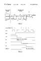
- the synchronization circuit 30includes a counter 31 , a first flip-flop 32 , a second flip-flop 34 , a third flip-flop 36 , and an XOR-gate 38 .
- the counter 31resides in a first clock domain, and is incremented according to a first clock signal (CLK 1 ).
- the flip-flops 32 - 36reside in a second clock domain and are edge-triggered devices responsive to a second clock signal (CLK 2 ).
- the clock signals CLK 1 and CLK 2are unsynchronized relative to one another. According to one embodiment, CLK 2 has a frequency greater than two times that of the LSB input.
- the flip-flopscan be any equivalent edge-triggered memory device, such as D flip-flops (shown), J-K flip-flops, or random access memory (RAM) cells.
- Each of the flip-flops 32 - 36is triggered by transitions of CLK 2 having the same direction, i.e., the flip-flops 32 - 36 all respond to either a positive edge or a negative edge of CLK 2 .
- the input to the first flip-flop 32is generated by the counter 31 .
- the counter 31can be any type of digital counter that is capable of incrementing its output value in response to a clock signal.
- the counter 31can include a ripple counter, carry look ahead adder, etc.
- the counter 31can produce a multi-bit output value that rolls over to zero upon reaching a predetermined maximum value.
- a single bit of the counter outputis provided as input to the first flip-flop 32 . Any of the counter output bits can be used by the first flip-flop 32 , including the least significant bit (LSB) of the counter output, as shown.
- the output of the XOR-gate 38represents the synchronization signal, and accordingly, is provided to circuitry within the second clock domain.
- FIG. 3illustrates an timing diagram depicting an example of the operational characteristics of the synchronization circuit 30 of FIG. 2 .
- CLK 2is a constant frequency signal.
- the LSB inputis not synchronized to CLK 2 , and a transition can occur on LSB at any time. In the example shown, a negative transition occurs on the LSB input during clock period 0 of CLK 2 . The LSB transition is triggered by a positive transition on CLK 1 .
- the flip-flops 32 - 36are triggered by the positive edges of CLK 2 .
- the LSB input transitionis clocked into the first flip-flop 32 at the leading positive edge of clock period 1 of CLK 2 .
- the first flip-flop 32may enter a metastable period, as shown in the trace line depicting output Q 0 .
- the transition on the LSB inputappears as the output of the second flip-flop 34 (Q 1 ).
- the LSB_SYNC outputtransitions to an active state.
- the LSB transitionappears on the output of the third flip-flop 36 (Q 2 ). This causes the XOR-gate to subsequently return its LSB_SYNC output to the inactive state.
- the circuit 10generates a one clock-period pulse in the second clock domain for each transition, positive and negative, occurring on the unsynchronized input (LSB).
- This feature of the circuit 10provides advantage over prior art synchronization circuits, such as those discussed earlier herein.
- FIG. 4illustrates a block diagram of an exemplary logic circuit 40 incorporating the synchronization circuit 30 in accordance with another embodiment of the present invention.
- the logic circuit 40includes a frame counter 41 , a shift register 42 , a buffer memory 44 and a state machine 46 .
- the frame counter 41 and shift register 42reside within a first clock domain (PCM clock domain), while the buffer memory 44 and the state machine 46 reside in a second clock domain (PCI clock domain).
- the synchronization circuit 30responds to a clock signal (PCI clock) originating in the second domain, and can be used to synchronize data transfers from the shift register 42 to the buffer memory 44 .
- PCI clockclock
- the synchronization circuit 30is usable within many different types of digital systems
- the circuit 40represents an interface between a pulse code modulated (PCM) data environment typically associated with telephony communications and a peripheral component interface (PCI) environment normally associated with personal computers.
- PCMpulse code modulated
- PCIperipheral component interface
- the first clock domainrepresents a circuit for handling PCM voice data.
- PCM voice datais information that encoded and transmitted according to well known industry standards for telephony communications, such as the T1 carrier standard developed by Bell Laboratories.
- the frame counter 41 and the shift register 42are synchronous devices that are responsive to the common PCM clock signal.
- the PCM clockcan operate at a standard frequency of 2 MHz.
- the frame counter 41is a conventional digital counter which increments its output once every clock period.
- the frame counterprovides an 8-bit output.
- the outputrepresents a bit position for the 256 bits included in a T1 standard PCM data frame.
- the least significant bit (LSB) of the counter output (FC 0 )is provided to the synchronization circuit 30 as the LSB input.
- the other output bits (FC 1 -FC 7 ) of the frame counter 41can be used as control signals in either clock domain.
- FC 1 -FC 3are provided to the state machine 46 as control inputs.
- the shift register 42is an example of one circuit that can exist within the PCM clock domain.
- the shift register 42serially shifts a PCM input bit during every PCM clock period.
- the shift register 42performs a serial to parallel conversion of incoming PCM serial data, and provides an 8-bit PCM output to the buffer memory 44 .
- the components within the PCI clock domaincan be included in a circuit operating in conformity with industry standards for the PCI bus protocol.
- the buffer memory 44 and the state machine 46are synchronous circuits which respond to the PCI clock.
- the PCI clockcan operate at a standard frequency of 33 MHz.
- the buffer memory 44receives parallel data output from the shift register 42 .
- the buffer memory 44can be any memory device for storing digital data, such as a register or random access memory (RAM).
- RAMrandom access memory
- the buffer memory 44is controlled by the state machine 46 .
- the LSB_SYNC output of the synchronization circuit 30is provided to the state machine 46 , as enable input.
- the state machine 46changes state and is responsive to FC 1 -FC 3 only when the LSB_SYNC signal is active.
- the state machine 46can be any finite state machine having a plurality of different states. In the example shown, the state machine 46 provides a control signal to the buffer memory 44 .
- Transitions between statescan be a function of FC 1 -FC 3 .
- the state machinecan have three states for detecting a predetermined sequence of three values appearing on FC 1 -FC 3 .
- the buffer control outputcan be enabled while the synchronization signal is active.
- the sequence detectionis accomplished by initializing the state machine to a first state.
- the state machine 46transitions to a second state upon detecting the first value in the sequence while the LSB_SYNC is active. If the next value on FC 1 -FC 3 is the second value in the sequence, the state machine 46 transitions to the third state. Otherwise, it returns to the first state.
- the state machine 46Upon reaching the third state, if the next value on FC 1 -FC 3 is the third value in the sequence, the state machine 46 enables the buffer control output and transitions back to the first state, where it waits for another sequence. If, while in the third state, the next value is not the third value, the state machine 46 returns to the first state without enabling the buffer control.
- the control signalwhen enabled, allows the buffer memory to latch data inputs received from the shift register 42 .
- the control signalis only enabled when the LSB_SYNC signal is active. In this fashion, the data outputs from the shift register 42 are read into the buffer memory 44 only when they are known to be valid and stable. Consequently, the otherwise unsynchronized inputs from the shift register 42 are synchronized with the operation of the buffer memory 44 .
- the counter outputs FC 0 -FC 7can also be used to provide an address (ADDR) to the buffer memory 44 .
- FC 3 -FC 7are provided to the memory 44 . This permits each byte shifted into shift register 42 to be stored at a unique location in the buffer memory 44 .
- the state machine 46can be configured to assert the memory control signal whenever it detects transitions on FC 3 .
- circuits shown in FIGS. 2 and 4can be implemented using any suitable logic circuitry, such as a combination of discrete logic components, or one or more application specific integrated circuits (ASICs).
- ASICsapplication specific integrated circuits
- the synchronization signalWhile the synchronization signal is active, the unsynchronized data inputs to the second clock domain are considered valid and stable.
- the synchronization signalcan be used to control other logic components within the second clock domain, permitting these elements to respond to unsynchronized data signals from the first clock domain while these inputs are known to be valid and stable.
Landscapes
- Engineering & Computer Science (AREA)
- Theoretical Computer Science (AREA)
- Physics & Mathematics (AREA)
- General Engineering & Computer Science (AREA)
- General Physics & Mathematics (AREA)
- Synchronisation In Digital Transmission Systems (AREA)
Abstract
Description
Claims (13)
Priority Applications (3)
| Application Number | Priority Date | Filing Date | Title |
|---|---|---|---|
| US09/126,430US6260152B1 (en) | 1998-07-30 | 1998-07-30 | Method and apparatus for synchronizing data transfers in a logic circuit having plural clock domains |
| EP99111776AEP0977109A1 (en) | 1998-07-30 | 1999-06-18 | Method and apparatus for synchronizing data transfers in a logic circuit having plural clock domains |
| JP11217252AJP2000099193A (en) | 1998-07-30 | 1999-07-30 | Device and method for synchronization, and interface circuit |
Applications Claiming Priority (1)
| Application Number | Priority Date | Filing Date | Title |
|---|---|---|---|
| US09/126,430US6260152B1 (en) | 1998-07-30 | 1998-07-30 | Method and apparatus for synchronizing data transfers in a logic circuit having plural clock domains |
Publications (1)
| Publication Number | Publication Date |
|---|---|
| US6260152B1true US6260152B1 (en) | 2001-07-10 |
Family
ID=22424794
Family Applications (1)
| Application Number | Title | Priority Date | Filing Date |
|---|---|---|---|
| US09/126,430Expired - LifetimeUS6260152B1 (en) | 1998-07-30 | 1998-07-30 | Method and apparatus for synchronizing data transfers in a logic circuit having plural clock domains |
Country Status (3)
| Country | Link |
|---|---|
| US (1) | US6260152B1 (en) |
| EP (1) | EP0977109A1 (en) |
| JP (1) | JP2000099193A (en) |
Cited By (60)
| Publication number | Priority date | Publication date | Assignee | Title |
|---|---|---|---|---|
| US6335645B1 (en)* | 1999-12-27 | 2002-01-01 | Mitsubishi Denki Kabushiki Kaisha | Semiconductor integrated circuit having built-in self-test circuit |
| US6393502B1 (en)* | 1999-08-31 | 2002-05-21 | Advanced Micro Devices, Inc. | System and method for initiating a serial data transfer between two clock domains |
| US20030056135A1 (en)* | 2001-09-14 | 2003-03-20 | Splett Vincent E. | Method and apparatus for synchronization of clock domains |
| US6571106B1 (en)* | 1999-07-14 | 2003-05-27 | Texas Instruments Incorporated | Method and apparatus for glitchless signal generation |
| US20030237014A1 (en)* | 2002-06-25 | 2003-12-25 | Lsi Logic Corporation | Minimum latency propagation of variable pulse width signals across clock domains with variable frequencies |
| US20040246810A1 (en)* | 2003-06-04 | 2004-12-09 | Dike Charles E. | Apparatus and method for reducing power consumption by a data synchronizer |
| US6907538B1 (en)* | 2001-10-16 | 2005-06-14 | Analog Devices, Inc. | Circuit and method for providing centralized synchronization for the transportation of data between devices in a different clock domains on a data bus |
| US20050280455A1 (en)* | 2004-05-24 | 2005-12-22 | Stmicroelectronics Limited | Asynchronous multi-clock system |
| US20060122667A1 (en)* | 2004-12-03 | 2006-06-08 | Cardiac Pacemakers, Inc. | Systems and methods for timing-based communication between implantable medical devices |
| US20070002634A1 (en)* | 2005-06-10 | 2007-01-04 | Luc Montperrus | System and method of transmitting data in an electronic circuit |
| US20070041264A1 (en)* | 2005-08-17 | 2007-02-22 | Cohen Daniel S | Method and apparatus for synchronizing data between different clock domains in a memory controller |
| US20070081414A1 (en)* | 2005-09-12 | 2007-04-12 | Cesar Douady | System and method of on-circuit asynchronous communication, between synchronous subcircuits |
| US20070130492A1 (en)* | 2005-12-02 | 2007-06-07 | Piyush Jamkhandi | Testable design methodology for clock domain crossing |
| US7250797B1 (en)* | 2001-03-30 | 2007-07-31 | Agere Systems Inc. | Event edge synchronization system and method of operation thereof |
| US20070245044A1 (en)* | 2006-04-12 | 2007-10-18 | Cesar Douady | System of interconnections for external functional blocks on a chip provided with a single configurable communication protocol |
| US20070248097A1 (en)* | 2006-03-31 | 2007-10-25 | Philippe Boucard | Message switching system |
| US20070271538A1 (en)* | 2006-05-16 | 2007-11-22 | Luc Montperrus | Process for designing a circuit for synchronizing data asychronously exchanged between two synchronous blocks, and synchronization circuit fabricated by same |
| US20070277053A1 (en)* | 2004-04-28 | 2007-11-29 | Daniel Timmermans | Circuit with asynchronous/synchronous interface |
| US20070297404A1 (en)* | 2006-06-23 | 2007-12-27 | Philippe Boucard | System and method for managing messages transmitted in an interconnect network |
| US20080028090A1 (en)* | 2006-07-26 | 2008-01-31 | Sophana Kok | System for managing messages transmitted in an on-chip interconnect network |
| US7366938B2 (en) | 2004-07-05 | 2008-04-29 | Stmicroelectronics Limited | Reset in a system-on-chip circuit |
| US20080171941A1 (en)* | 2007-01-12 | 2008-07-17 | Huelskamp Paul J | Low power methods for pressure waveform signal sampling using implantable medical devices |
| US7617001B2 (en) | 2000-10-16 | 2009-11-10 | Remon Medical Technologies, Ltd | Systems and method for communicating with implantable devices |
| US7650185B2 (en) | 2006-04-25 | 2010-01-19 | Cardiac Pacemakers, Inc. | System and method for walking an implantable medical device from a sleep state |
| US7930031B2 (en) | 2000-10-16 | 2011-04-19 | Remon Medical Technologies, Ltd. | Acoustically powered implantable stimulating device |
| USRE42378E1 (en) | 2000-10-16 | 2011-05-17 | Remon Medical Technologies, Ltd. | Implantable pressure sensors and methods for making and using them |
| US8078278B2 (en) | 2006-01-10 | 2011-12-13 | Remon Medical Technologies Ltd. | Body attachable unit in wireless communication with implantable devices |
| US20120005545A1 (en)* | 2010-07-02 | 2012-01-05 | Fujitsu Limited | Computer product, verification support apparatus, and verification support method |
| US8340776B2 (en) | 2007-03-26 | 2012-12-25 | Cardiac Pacemakers, Inc. | Biased acoustic switch for implantable medical device |
| US8593107B2 (en) | 2008-10-27 | 2013-11-26 | Cardiac Pacemakers, Inc. | Methods and systems for recharging an implanted device by delivering a section of a charging device adjacent the implanted device within a body |
| US8798761B2 (en) | 2008-06-27 | 2014-08-05 | Cardiac Pacemakers, Inc. | Systems and methods of monitoring the acoustic coupling of medical devices |
| US10009032B2 (en)* | 2016-08-17 | 2018-06-26 | Oracle International Corporation | Alignment of samples across different clock domains |
| US10346226B2 (en)* | 2017-08-07 | 2019-07-09 | Time Warner Cable Enterprises Llc | Methods and apparatus for transmitting time sensitive data over a tunneled bus interface |
| US10371748B2 (en)* | 2007-06-07 | 2019-08-06 | Texas Instruments Incorporated | Monitoring communication link in powered-up device for synchronization point sequence |
| US10372637B2 (en) | 2014-09-16 | 2019-08-06 | Apple Inc. | Methods and apparatus for aggregating packet transfer over a virtual bus interface |
| US10430352B1 (en) | 2018-05-18 | 2019-10-01 | Apple Inc. | Methods and apparatus for reduced overhead data transfer with a shared ring buffer |
| US10551902B2 (en) | 2016-11-10 | 2020-02-04 | Apple Inc. | Methods and apparatus for providing access to peripheral sub-system registers |
| US10552352B2 (en) | 2015-06-12 | 2020-02-04 | Apple Inc. | Methods and apparatus for synchronizing uplink and downlink transactions on an inter-device communication link |
| US10551906B2 (en) | 2014-10-08 | 2020-02-04 | Apple Inc. | Methods and apparatus for running and booting inter-processor communication link between independently operable processors |
| US10558580B2 (en) | 2016-02-29 | 2020-02-11 | Apple Inc. | Methods and apparatus for loading firmware on demand |
| US10585699B2 (en) | 2018-07-30 | 2020-03-10 | Apple Inc. | Methods and apparatus for verifying completion of groups of data transactions between processors |
| US10719376B2 (en) | 2018-08-24 | 2020-07-21 | Apple Inc. | Methods and apparatus for multiplexing data flows via a single data structure |
| US10775871B2 (en) | 2016-11-10 | 2020-09-15 | Apple Inc. | Methods and apparatus for providing individualized power control for peripheral sub-systems |
| US10789110B2 (en) | 2018-09-28 | 2020-09-29 | Apple Inc. | Methods and apparatus for correcting out-of-order data transactions between processors |
| US10789198B2 (en) | 2018-01-09 | 2020-09-29 | Apple Inc. | Methods and apparatus for reduced-latency data transmission with an inter-processor communication link between independently operable processors |
| US10838450B2 (en) | 2018-09-28 | 2020-11-17 | Apple Inc. | Methods and apparatus for synchronization of time between independently operable processors |
| US10841880B2 (en) | 2016-01-27 | 2020-11-17 | Apple Inc. | Apparatus and methods for wake-limiting with an inter-device communication link |
| US10846224B2 (en) | 2018-08-24 | 2020-11-24 | Apple Inc. | Methods and apparatus for control of a jointly shared memory-mapped region |
| US10853272B2 (en) | 2016-03-31 | 2020-12-01 | Apple Inc. | Memory access protection apparatus and methods for memory mapped access between independently operable processors |
| US11381514B2 (en) | 2018-05-07 | 2022-07-05 | Apple Inc. | Methods and apparatus for early delivery of data link layer packets |
| US11558348B2 (en) | 2019-09-26 | 2023-01-17 | Apple Inc. | Methods and apparatus for emerging use case support in user space networking |
| US11606302B2 (en) | 2020-06-12 | 2023-03-14 | Apple Inc. | Methods and apparatus for flow-based batching and processing |
| CN116126116A (en)* | 2023-02-03 | 2023-05-16 | 芯动微电子科技(武汉)有限公司 | Clock reset circuit, method, device, system-in-chip and storage medium |
| US11775359B2 (en) | 2020-09-11 | 2023-10-03 | Apple Inc. | Methods and apparatuses for cross-layer processing |
| US11792307B2 (en) | 2018-03-28 | 2023-10-17 | Apple Inc. | Methods and apparatus for single entity buffer pool management |
| US11799986B2 (en) | 2020-09-22 | 2023-10-24 | Apple Inc. | Methods and apparatus for thread level execution in non-kernel space |
| US11829303B2 (en) | 2019-09-26 | 2023-11-28 | Apple Inc. | Methods and apparatus for device driver operation in non-kernel space |
| US11876719B2 (en) | 2021-07-26 | 2024-01-16 | Apple Inc. | Systems and methods for managing transmission control protocol (TCP) acknowledgements |
| US11882051B2 (en) | 2021-07-26 | 2024-01-23 | Apple Inc. | Systems and methods for managing transmission control protocol (TCP) acknowledgements |
| US11954540B2 (en) | 2020-09-14 | 2024-04-09 | Apple Inc. | Methods and apparatus for thread-level execution in non-kernel space |
Families Citing this family (4)
| Publication number | Priority date | Publication date | Assignee | Title |
|---|---|---|---|---|
| EP1188108B1 (en)* | 2000-04-17 | 2003-11-26 | Italtel s.p.a. | Two clock domain pulse to pulse synchronizer |
| JP2011039900A (en)* | 2009-08-17 | 2011-02-24 | Fuji Xerox Co Ltd | Network system, and program for the same |
| CN102916700B (en)* | 2011-08-05 | 2015-07-29 | 炬芯(珠海)科技有限公司 | Data transmission device and method |
| GB2503473A (en)* | 2012-06-27 | 2014-01-01 | Nordic Semiconductor Asa | Data transfer from lower frequency clock domain to higher frequency clock domain |
Citations (17)
| Publication number | Priority date | Publication date | Assignee | Title |
|---|---|---|---|---|
| US3665405A (en) | 1970-03-17 | 1972-05-23 | Computer Transmission Corp | Multiplexer |
| US3751597A (en) | 1971-12-30 | 1973-08-07 | Bell Telephone Labor Inc | Time division multiplex network switching unit |
| US3914553A (en) | 1973-09-24 | 1975-10-21 | Cselt Centro Studi Lab Telecom | Multiplexing/demultiplexing network with series/parallel conversion for TDM system |
| US4021784A (en)* | 1976-03-12 | 1977-05-03 | Sperry Rand Corporation | Clock synchronization system |
| US4589019A (en)* | 1983-04-22 | 1986-05-13 | Rca Corporation | Digital adder including counter coupled to individual bits of the input |
| US5638015A (en) | 1995-06-21 | 1997-06-10 | Unisys Corporation | Avoiding instability |
| US5668982A (en)* | 1995-11-30 | 1997-09-16 | National Semiconductor Corporation | System and method for using a half-clock module to implement computer timing control circuitry |
| US5790842A (en)* | 1996-10-11 | 1998-08-04 | Divicom, Inc. | Processing system with simultaneous utilization of multiple clock signals |
| US5835752A (en)* | 1996-10-18 | 1998-11-10 | Samsung Electronics Co. Ltd. | PCI interface synchronization |
| US5860003A (en)* | 1997-02-28 | 1999-01-12 | Mti Technology, Inc. | I/O controller software with each I/O command having a plurality of nets, each with a group of threads |
| US5909563A (en)* | 1996-09-25 | 1999-06-01 | Philips Electronics North America Corporation | Computer system including an interface for transferring data between two clock domains |
| US5987081A (en)* | 1997-06-27 | 1999-11-16 | Sun Microsystems, Inc. | Method and apparatus for a testable high frequency synchronizer |
| US6021503A (en)* | 1996-12-21 | 2000-02-01 | Micron Communications, Inc. | Bit synchronization for interrogator |
| US6055285A (en)* | 1997-11-17 | 2000-04-25 | Qlogic Corporation | Synchronization circuit for transferring pointer between two asynchronous circuits |
| US6078623A (en)* | 1995-03-20 | 2000-06-20 | Hitachi, Ltd. | Data transmission apparatus and method |
| US6098139A (en)* | 1998-05-27 | 2000-08-01 | 3Com Corporation | Frequency independent asynchronous clock crossing FIFO |
| US6107855A (en)* | 1996-06-28 | 2000-08-22 | Emc Corporation | Redundant clock signal generating circuitry |
Family Cites Families (3)
| Publication number | Priority date | Publication date | Assignee | Title |
|---|---|---|---|---|
| JPH0758914B2 (en)* | 1984-12-27 | 1995-06-21 | 株式会社東芝 | PCM Dynasim Shimureta |
| US5680644A (en)* | 1994-10-31 | 1997-10-21 | Digital Equipment Corporation | Low delay means of communicating between systems on different clocks |
| US5905766A (en)* | 1996-03-29 | 1999-05-18 | Fore Systems, Inc. | Synchronizer, method and system for transferring data |
- 1998
- 1998-07-30USUS09/126,430patent/US6260152B1/ennot_activeExpired - Lifetime
- 1999
- 1999-06-18EPEP99111776Apatent/EP0977109A1/ennot_activeWithdrawn
- 1999-07-30JPJP11217252Apatent/JP2000099193A/enactivePending
Patent Citations (17)
| Publication number | Priority date | Publication date | Assignee | Title |
|---|---|---|---|---|
| US3665405A (en) | 1970-03-17 | 1972-05-23 | Computer Transmission Corp | Multiplexer |
| US3751597A (en) | 1971-12-30 | 1973-08-07 | Bell Telephone Labor Inc | Time division multiplex network switching unit |
| US3914553A (en) | 1973-09-24 | 1975-10-21 | Cselt Centro Studi Lab Telecom | Multiplexing/demultiplexing network with series/parallel conversion for TDM system |
| US4021784A (en)* | 1976-03-12 | 1977-05-03 | Sperry Rand Corporation | Clock synchronization system |
| US4589019A (en)* | 1983-04-22 | 1986-05-13 | Rca Corporation | Digital adder including counter coupled to individual bits of the input |
| US6078623A (en)* | 1995-03-20 | 2000-06-20 | Hitachi, Ltd. | Data transmission apparatus and method |
| US5638015A (en) | 1995-06-21 | 1997-06-10 | Unisys Corporation | Avoiding instability |
| US5668982A (en)* | 1995-11-30 | 1997-09-16 | National Semiconductor Corporation | System and method for using a half-clock module to implement computer timing control circuitry |
| US6107855A (en)* | 1996-06-28 | 2000-08-22 | Emc Corporation | Redundant clock signal generating circuitry |
| US5909563A (en)* | 1996-09-25 | 1999-06-01 | Philips Electronics North America Corporation | Computer system including an interface for transferring data between two clock domains |
| US5790842A (en)* | 1996-10-11 | 1998-08-04 | Divicom, Inc. | Processing system with simultaneous utilization of multiple clock signals |
| US5835752A (en)* | 1996-10-18 | 1998-11-10 | Samsung Electronics Co. Ltd. | PCI interface synchronization |
| US6021503A (en)* | 1996-12-21 | 2000-02-01 | Micron Communications, Inc. | Bit synchronization for interrogator |
| US5860003A (en)* | 1997-02-28 | 1999-01-12 | Mti Technology, Inc. | I/O controller software with each I/O command having a plurality of nets, each with a group of threads |
| US5987081A (en)* | 1997-06-27 | 1999-11-16 | Sun Microsystems, Inc. | Method and apparatus for a testable high frequency synchronizer |
| US6055285A (en)* | 1997-11-17 | 2000-04-25 | Qlogic Corporation | Synchronization circuit for transferring pointer between two asynchronous circuits |
| US6098139A (en)* | 1998-05-27 | 2000-08-01 | 3Com Corporation | Frequency independent asynchronous clock crossing FIFO |
Cited By (101)
| Publication number | Priority date | Publication date | Assignee | Title |
|---|---|---|---|---|
| US6571106B1 (en)* | 1999-07-14 | 2003-05-27 | Texas Instruments Incorporated | Method and apparatus for glitchless signal generation |
| US6393502B1 (en)* | 1999-08-31 | 2002-05-21 | Advanced Micro Devices, Inc. | System and method for initiating a serial data transfer between two clock domains |
| US6335645B1 (en)* | 1999-12-27 | 2002-01-01 | Mitsubishi Denki Kabushiki Kaisha | Semiconductor integrated circuit having built-in self-test circuit |
| US7756587B2 (en) | 2000-10-16 | 2010-07-13 | Cardiac Pacemakers, Inc. | Systems and methods for communicating with implantable devices |
| US8934972B2 (en) | 2000-10-16 | 2015-01-13 | Remon Medical Technologies, Ltd. | Acoustically powered implantable stimulating device |
| US7617001B2 (en) | 2000-10-16 | 2009-11-10 | Remon Medical Technologies, Ltd | Systems and method for communicating with implantable devices |
| US7930031B2 (en) | 2000-10-16 | 2011-04-19 | Remon Medical Technologies, Ltd. | Acoustically powered implantable stimulating device |
| USRE42378E1 (en) | 2000-10-16 | 2011-05-17 | Remon Medical Technologies, Ltd. | Implantable pressure sensors and methods for making and using them |
| US8577460B2 (en) | 2000-10-16 | 2013-11-05 | Remon Medical Technologies, Ltd | Acoustically powered implantable stimulating device |
| US7724855B2 (en) | 2001-03-30 | 2010-05-25 | Agere Systems Inc. | Event edge synchronization system and method of operation thereof |
| US7250797B1 (en)* | 2001-03-30 | 2007-07-31 | Agere Systems Inc. | Event edge synchronization system and method of operation thereof |
| US20080012614A1 (en)* | 2001-03-30 | 2008-01-17 | Agere Systems Inc. | Event edge synchronization system and method of operation thereof |
| US20030056135A1 (en)* | 2001-09-14 | 2003-03-20 | Splett Vincent E. | Method and apparatus for synchronization of clock domains |
| US6988215B2 (en)* | 2001-09-14 | 2006-01-17 | Medtronic, Inc. | Method and apparatus for synchronization of clock domains |
| US6907538B1 (en)* | 2001-10-16 | 2005-06-14 | Analog Devices, Inc. | Circuit and method for providing centralized synchronization for the transportation of data between devices in a different clock domains on a data bus |
| US20030237014A1 (en)* | 2002-06-25 | 2003-12-25 | Lsi Logic Corporation | Minimum latency propagation of variable pulse width signals across clock domains with variable frequencies |
| US6901528B2 (en)* | 2002-06-25 | 2005-05-31 | Lsi Logic Corporation | Minimum latency propagation of variable pulse width signals across clock domains with variable frequencies |
| US6989695B2 (en)* | 2003-06-04 | 2006-01-24 | Intel Corporation | Apparatus and method for reducing power consumption by a data synchronizer |
| US20040246810A1 (en)* | 2003-06-04 | 2004-12-09 | Dike Charles E. | Apparatus and method for reducing power consumption by a data synchronizer |
| US20070277053A1 (en)* | 2004-04-28 | 2007-11-29 | Daniel Timmermans | Circuit with asynchronous/synchronous interface |
| US7929655B2 (en) | 2004-05-24 | 2011-04-19 | Stmicroelectronics Limited | Asynchronous multi-clock system |
| US7545896B2 (en)* | 2004-05-24 | 2009-06-09 | Stmicroelectronics Limited | Asynchronous multi-clock system |
| US20090316845A1 (en)* | 2004-05-24 | 2009-12-24 | Stmicroelectronics Limited | Asynchronous multi-clock system |
| US20050280455A1 (en)* | 2004-05-24 | 2005-12-22 | Stmicroelectronics Limited | Asynchronous multi-clock system |
| US7366938B2 (en) | 2004-07-05 | 2008-04-29 | Stmicroelectronics Limited | Reset in a system-on-chip circuit |
| US20060122667A1 (en)* | 2004-12-03 | 2006-06-08 | Cardiac Pacemakers, Inc. | Systems and methods for timing-based communication between implantable medical devices |
| US8374693B2 (en) | 2004-12-03 | 2013-02-12 | Cardiac Pacemakers, Inc. | Systems and methods for timing-based communication between implantable medical devices |
| US20070002634A1 (en)* | 2005-06-10 | 2007-01-04 | Luc Montperrus | System and method of transmitting data in an electronic circuit |
| US20070041264A1 (en)* | 2005-08-17 | 2007-02-22 | Cohen Daniel S | Method and apparatus for synchronizing data between different clock domains in a memory controller |
| US7639764B2 (en)* | 2005-08-17 | 2009-12-29 | Atmel Corporation | Method and apparatus for synchronizing data between different clock domains in a memory controller |
| US20070081414A1 (en)* | 2005-09-12 | 2007-04-12 | Cesar Douady | System and method of on-circuit asynchronous communication, between synchronous subcircuits |
| US20070130492A1 (en)* | 2005-12-02 | 2007-06-07 | Piyush Jamkhandi | Testable design methodology for clock domain crossing |
| US7293214B2 (en)* | 2005-12-02 | 2007-11-06 | Broadcom Corporation | Testable design methodology for clock domain crossing |
| US8078278B2 (en) | 2006-01-10 | 2011-12-13 | Remon Medical Technologies Ltd. | Body attachable unit in wireless communication with implantable devices |
| US7639704B2 (en) | 2006-03-31 | 2009-12-29 | Arteris | Message switching system |
| US20070248097A1 (en)* | 2006-03-31 | 2007-10-25 | Philippe Boucard | Message switching system |
| US20100122004A1 (en)* | 2006-03-31 | 2010-05-13 | Arteris | Message switching system |
| US20070245044A1 (en)* | 2006-04-12 | 2007-10-18 | Cesar Douady | System of interconnections for external functional blocks on a chip provided with a single configurable communication protocol |
| US8645557B2 (en) | 2006-04-12 | 2014-02-04 | Qualcomm Technologies, Inc. | System of interconnections for external functional blocks on a chip provided with a single configurable communication protocol |
| US7650185B2 (en) | 2006-04-25 | 2010-01-19 | Cardiac Pacemakers, Inc. | System and method for walking an implantable medical device from a sleep state |
| US20070271538A1 (en)* | 2006-05-16 | 2007-11-22 | Luc Montperrus | Process for designing a circuit for synchronizing data asychronously exchanged between two synchronous blocks, and synchronization circuit fabricated by same |
| US8254380B2 (en) | 2006-06-23 | 2012-08-28 | Arteris | Managing messages transmitted in an interconnect network |
| US20070297404A1 (en)* | 2006-06-23 | 2007-12-27 | Philippe Boucard | System and method for managing messages transmitted in an interconnect network |
| US20080028090A1 (en)* | 2006-07-26 | 2008-01-31 | Sophana Kok | System for managing messages transmitted in an on-chip interconnect network |
| US20080171941A1 (en)* | 2007-01-12 | 2008-07-17 | Huelskamp Paul J | Low power methods for pressure waveform signal sampling using implantable medical devices |
| US8340776B2 (en) | 2007-03-26 | 2012-12-25 | Cardiac Pacemakers, Inc. | Biased acoustic switch for implantable medical device |
| US11867759B2 (en) | 2007-06-07 | 2024-01-09 | Texas Instruments Incorporated | Synchronizing a device that has been power cycled to an already operational system |
| US10955471B2 (en) | 2007-06-07 | 2021-03-23 | Texas Instruments Incorporated | Operating state machine controllers after powering, decoupling, monitoring, coupling communications |
| US11567129B2 (en) | 2007-06-07 | 2023-01-31 | Texas Instruments Incorporated | Synchronizing a device that has been power cycled to an already operational system |
| US10371748B2 (en)* | 2007-06-07 | 2019-08-06 | Texas Instruments Incorporated | Monitoring communication link in powered-up device for synchronization point sequence |
| US8798761B2 (en) | 2008-06-27 | 2014-08-05 | Cardiac Pacemakers, Inc. | Systems and methods of monitoring the acoustic coupling of medical devices |
| US9024582B2 (en) | 2008-10-27 | 2015-05-05 | Cardiac Pacemakers, Inc. | Methods and systems for recharging an implanted device by delivering a section of a charging device adjacent the implanted device within a body |
| US8593107B2 (en) | 2008-10-27 | 2013-11-26 | Cardiac Pacemakers, Inc. | Methods and systems for recharging an implanted device by delivering a section of a charging device adjacent the implanted device within a body |
| US20120005545A1 (en)* | 2010-07-02 | 2012-01-05 | Fujitsu Limited | Computer product, verification support apparatus, and verification support method |
| US8533541B2 (en)* | 2010-07-02 | 2013-09-10 | Fujitsu Limited | Verification support of circuit blocks having independent clock domains |
| US10372637B2 (en) | 2014-09-16 | 2019-08-06 | Apple Inc. | Methods and apparatus for aggregating packet transfer over a virtual bus interface |
| US10551906B2 (en) | 2014-10-08 | 2020-02-04 | Apple Inc. | Methods and apparatus for running and booting inter-processor communication link between independently operable processors |
| US10845868B2 (en) | 2014-10-08 | 2020-11-24 | Apple Inc. | Methods and apparatus for running and booting an inter-processor communication link between independently operable processors |
| US10684670B2 (en) | 2014-10-08 | 2020-06-16 | Apple Inc. | Methods and apparatus for managing power with an inter-processor communication link between independently operable processors |
| US11176068B2 (en) | 2015-06-12 | 2021-11-16 | Apple Inc. | Methods and apparatus for synchronizing uplink and downlink transactions on an inter-device communication link |
| US10552352B2 (en) | 2015-06-12 | 2020-02-04 | Apple Inc. | Methods and apparatus for synchronizing uplink and downlink transactions on an inter-device communication link |
| US10841880B2 (en) | 2016-01-27 | 2020-11-17 | Apple Inc. | Apparatus and methods for wake-limiting with an inter-device communication link |
| US10572390B2 (en) | 2016-02-29 | 2020-02-25 | Apple Inc. | Methods and apparatus for loading firmware on demand |
| US10558580B2 (en) | 2016-02-29 | 2020-02-11 | Apple Inc. | Methods and apparatus for loading firmware on demand |
| US10853272B2 (en) | 2016-03-31 | 2020-12-01 | Apple Inc. | Memory access protection apparatus and methods for memory mapped access between independently operable processors |
| US10009032B2 (en)* | 2016-08-17 | 2018-06-26 | Oracle International Corporation | Alignment of samples across different clock domains |
| US11809258B2 (en) | 2016-11-10 | 2023-11-07 | Apple Inc. | Methods and apparatus for providing peripheral sub-system stability |
| US10591976B2 (en) | 2016-11-10 | 2020-03-17 | Apple Inc. | Methods and apparatus for providing peripheral sub-system stability |
| US10775871B2 (en) | 2016-11-10 | 2020-09-15 | Apple Inc. | Methods and apparatus for providing individualized power control for peripheral sub-systems |
| US10551902B2 (en) | 2016-11-10 | 2020-02-04 | Apple Inc. | Methods and apparatus for providing access to peripheral sub-system registers |
| US11068326B2 (en) | 2017-08-07 | 2021-07-20 | Apple Inc. | Methods and apparatus for transmitting time sensitive data over a tunneled bus interface |
| US11314567B2 (en) | 2017-08-07 | 2022-04-26 | Apple Inc. | Methods and apparatus for scheduling time sensitive operations among independent processors |
| US10346226B2 (en)* | 2017-08-07 | 2019-07-09 | Time Warner Cable Enterprises Llc | Methods and apparatus for transmitting time sensitive data over a tunneled bus interface |
| US10489223B2 (en) | 2017-08-07 | 2019-11-26 | Apple Inc. | Methods and apparatus for scheduling time sensitive operations among independent processors |
| US10789198B2 (en) | 2018-01-09 | 2020-09-29 | Apple Inc. | Methods and apparatus for reduced-latency data transmission with an inter-processor communication link between independently operable processors |
| US11824962B2 (en) | 2018-03-28 | 2023-11-21 | Apple Inc. | Methods and apparatus for sharing and arbitration of host stack information with user space communication stacks |
| US11843683B2 (en) | 2018-03-28 | 2023-12-12 | Apple Inc. | Methods and apparatus for active queue management in user space networking |
| US12314786B2 (en) | 2018-03-28 | 2025-05-27 | Apple Inc. | Methods and apparatus for memory allocation and reallocation in networking stack infrastructures |
| US11792307B2 (en) | 2018-03-28 | 2023-10-17 | Apple Inc. | Methods and apparatus for single entity buffer pool management |
| US11381514B2 (en) | 2018-05-07 | 2022-07-05 | Apple Inc. | Methods and apparatus for early delivery of data link layer packets |
| US10430352B1 (en) | 2018-05-18 | 2019-10-01 | Apple Inc. | Methods and apparatus for reduced overhead data transfer with a shared ring buffer |
| US11176064B2 (en) | 2018-05-18 | 2021-11-16 | Apple Inc. | Methods and apparatus for reduced overhead data transfer with a shared ring buffer |
| US10585699B2 (en) | 2018-07-30 | 2020-03-10 | Apple Inc. | Methods and apparatus for verifying completion of groups of data transactions between processors |
| US10719376B2 (en) | 2018-08-24 | 2020-07-21 | Apple Inc. | Methods and apparatus for multiplexing data flows via a single data structure |
| US11347567B2 (en) | 2018-08-24 | 2022-05-31 | Apple Inc. | Methods and apparatus for multiplexing data flows via a single data structure |
| US10846224B2 (en) | 2018-08-24 | 2020-11-24 | Apple Inc. | Methods and apparatus for control of a jointly shared memory-mapped region |
| US10838450B2 (en) | 2018-09-28 | 2020-11-17 | Apple Inc. | Methods and apparatus for synchronization of time between independently operable processors |
| US11379278B2 (en) | 2018-09-28 | 2022-07-05 | Apple Inc. | Methods and apparatus for correcting out-of-order data transactions between processors |
| US11243560B2 (en) | 2018-09-28 | 2022-02-08 | Apple Inc. | Methods and apparatus for synchronization of time between independently operable processors |
| US10789110B2 (en) | 2018-09-28 | 2020-09-29 | Apple Inc. | Methods and apparatus for correcting out-of-order data transactions between processors |
| US11829303B2 (en) | 2019-09-26 | 2023-11-28 | Apple Inc. | Methods and apparatus for device driver operation in non-kernel space |
| US11558348B2 (en) | 2019-09-26 | 2023-01-17 | Apple Inc. | Methods and apparatus for emerging use case support in user space networking |
| US11606302B2 (en) | 2020-06-12 | 2023-03-14 | Apple Inc. | Methods and apparatus for flow-based batching and processing |
| US11775359B2 (en) | 2020-09-11 | 2023-10-03 | Apple Inc. | Methods and apparatuses for cross-layer processing |
| US11954540B2 (en) | 2020-09-14 | 2024-04-09 | Apple Inc. | Methods and apparatus for thread-level execution in non-kernel space |
| US11799986B2 (en) | 2020-09-22 | 2023-10-24 | Apple Inc. | Methods and apparatus for thread level execution in non-kernel space |
| US11876719B2 (en) | 2021-07-26 | 2024-01-16 | Apple Inc. | Systems and methods for managing transmission control protocol (TCP) acknowledgements |
| US11882051B2 (en) | 2021-07-26 | 2024-01-23 | Apple Inc. | Systems and methods for managing transmission control protocol (TCP) acknowledgements |
| US12316548B2 (en) | 2021-07-26 | 2025-05-27 | Apple Inc. | Systems and methods for managing transmission control protocol (TCP) acknowledgements |
| CN116126116B (en)* | 2023-02-03 | 2023-12-01 | 芯动微电子科技(武汉)有限公司 | Clock reset circuit, method, device, system-in-chip and storage medium |
| CN116126116A (en)* | 2023-02-03 | 2023-05-16 | 芯动微电子科技(武汉)有限公司 | Clock reset circuit, method, device, system-in-chip and storage medium |
Also Published As
| Publication number | Publication date |
|---|---|
| EP0977109A1 (en) | 2000-02-02 |
| JP2000099193A (en) | 2000-04-07 |
Similar Documents
| Publication | Publication Date | Title |
|---|---|---|
| US6260152B1 (en) | Method and apparatus for synchronizing data transfers in a logic circuit having plural clock domains | |
| JP3156813B2 (en) | Buffer control circuit | |
| US6240523B1 (en) | Method and apparatus for automatically determining the phase relationship between two clocks generated from the same source | |
| JPH07253947A (en) | Data communication equipment | |
| JP3645584B2 (en) | Data transfer synchronization device | |
| US6864735B2 (en) | Circuit and method for regenerating reset and clock signals and high-speed digital system incorporating the same | |
| CN114185397B (en) | Cross-clock domain data transmission circuit and method | |
| US7242737B2 (en) | System and method for data phase realignment | |
| JP3080341B2 (en) | Data match detection circuit | |
| US6163584A (en) | Synchronization element for converting an asynchronous pulse signal into a synchronous pulse signal | |
| US6075833A (en) | Method and apparatus for counting signal transitions | |
| US5781765A (en) | System for data synchronization between two devices using four time domains | |
| US6232796B1 (en) | Apparatus and method for detecting two data bits per clock edge | |
| US6952791B2 (en) | Method and circuit for initializing a de-skewing buffer in a clock forwarded system | |
| US7696801B2 (en) | Reset method for clock triggering digital circuit and related signal generating apparatus utilizing the reset method | |
| US6205192B1 (en) | Clock input control circuit | |
| US6920578B1 (en) | Method and apparatus for transferring data between a slower clock domain and a faster clock domain in which one of the clock domains is bandwidth limited | |
| US6519301B1 (en) | Circuits, systems, and methods for passing request information across differing clock domains | |
| US6747490B1 (en) | Sampling pulse generation | |
| EP0839424A1 (en) | Extended chip select reset apparatus and method | |
| JPH1168861A (en) | Simultaneous bidirectional transmission / reception method and simultaneous bidirectional transmission / reception circuit | |
| JP2783495B2 (en) | Clock transfer circuit | |
| KR20010006850A (en) | Improved skew pointer generation | |
| JP2596336B2 (en) | Asynchronous digital communication device | |
| JPH04316126A (en) | Code converting device |
Legal Events
| Date | Code | Title | Description |
|---|---|---|---|
| AS | Assignment | Owner name:SIEMENS BUSINESS COMMUNICATION SYSTEMS, INC., CALI Free format text:ASSIGNMENT OF ASSIGNORS INTEREST;ASSIGNORS:COLE, STEVEN R.;BACA, RUSSELL T.;REEL/FRAME:009354/0586;SIGNING DATES FROM 19980722 TO 19980723 | |
| AS | Assignment | Owner name:SIEMENS INFORMATION AND COMMUNICATION NETWORKS, IN Free format text:CERTIFICATE OF MERGER;ASSIGNOR:SIEMENS BUSINESS COMMUNICATION SYSTEMS, INC.;REEL/FRAME:011573/0915 Effective date:19980930 | |
| STCF | Information on status: patent grant | Free format text:PATENTED CASE | |
| FPAY | Fee payment | Year of fee payment:4 | |
| FPAY | Fee payment | Year of fee payment:8 | |
| AS | Assignment | Owner name:SIEMENS COMMUNICATIONS, INC.,FLORIDA Free format text:MERGER;ASSIGNOR:SIEMENS INFORMATION AND COMMUNICATION NETWORKS, INC.;REEL/FRAME:024263/0817 Effective date:20040922 Owner name:SIEMENS COMMUNICATIONS, INC., FLORIDA Free format text:MERGER;ASSIGNOR:SIEMENS INFORMATION AND COMMUNICATION NETWORKS, INC.;REEL/FRAME:024263/0817 Effective date:20040922 | |
| AS | Assignment | Owner name:SIEMENS ENTERPRISE COMMUNICATIONS, INC.,FLORIDA Free format text:ASSIGNMENT OF ASSIGNORS INTEREST;ASSIGNOR:SIEMENS COMMUNICATIONS, INC.;REEL/FRAME:024294/0040 Effective date:20100304 Owner name:SIEMENS ENTERPRISE COMMUNICATIONS, INC., FLORIDA Free format text:ASSIGNMENT OF ASSIGNORS INTEREST;ASSIGNOR:SIEMENS COMMUNICATIONS, INC.;REEL/FRAME:024294/0040 Effective date:20100304 | |
| AS | Assignment | Owner name:WELLS FARGO TRUST CORPORATION LIMITED, AS SECURITY Free format text:GRANT OF SECURITY INTEREST IN U.S. PATENTS;ASSIGNOR:SIEMENS ENTERPRISE COMMUNICATIONS, INC.;REEL/FRAME:025339/0904 Effective date:20101109 | |
| REMI | Maintenance fee reminder mailed | ||
| FPAY | Fee payment | Year of fee payment:12 | |
| SULP | Surcharge for late payment | Year of fee payment:11 | |
| AS | Assignment | Owner name:UNIFY, INC., FLORIDA Free format text:CHANGE OF NAME;ASSIGNOR:SIEMENS ENTERPRISE COMMUNICATIONS, INC.;REEL/FRAME:037090/0909 Effective date:20131015 | |
| AS | Assignment | Owner name:UNIFY INC. (F/K/A SIEMENS ENTERPRISE COMMUNICATION Free format text:TERMINATION AND RELEASE OF SECURITY INTEREST IN PATENTS;ASSIGNOR:WELLS FARGO TRUST CORPORATION LIMITED, AS SECURITY AGENT;REEL/FRAME:037564/0703 Effective date:20160120 | |
| AS | Assignment | Owner name:UNIFY INC., FLORIDA Free format text:RELEASE BY SECURED PARTY;ASSIGNOR:WELLS FARGO TRUST CORPORATION LIMITED;REEL/FRAME:037661/0781 Effective date:20160120 |