US6259804B1 - Fingerprint sensor with gain control features and associated methods - Google Patents
Fingerprint sensor with gain control features and associated methodsDownload PDFInfo
- Publication number
- US6259804B1 US6259804B1US08/858,142US85814297AUS6259804B1US 6259804 B1US6259804 B1US 6259804B1US 85814297 AUS85814297 AUS 85814297AUS 6259804 B1US6259804 B1US 6259804B1
- Authority
- US
- United States
- Prior art keywords
- range
- fingerprint
- sensing elements
- reference voltage
- fingerprint sensor
- Prior art date
- Legal status (The legal status is an assumption and is not a legal conclusion. Google has not performed a legal analysis and makes no representation as to the accuracy of the status listed.)
- Expired - Lifetime
Links
Images


Classifications
- G—PHYSICS
- G06—COMPUTING OR CALCULATING; COUNTING
- G06V—IMAGE OR VIDEO RECOGNITION OR UNDERSTANDING
- G06V40/00—Recognition of biometric, human-related or animal-related patterns in image or video data
- G06V40/10—Human or animal bodies, e.g. vehicle occupants or pedestrians; Body parts, e.g. hands
- G06V40/12—Fingerprints or palmprints
- G06V40/13—Sensors therefor
- G06V40/1306—Sensors therefor non-optical, e.g. ultrasonic or capacitive sensing
- G—PHYSICS
- G07—CHECKING-DEVICES
- G07C—TIME OR ATTENDANCE REGISTERS; REGISTERING OR INDICATING THE WORKING OF MACHINES; GENERATING RANDOM NUMBERS; VOTING OR LOTTERY APPARATUS; ARRANGEMENTS, SYSTEMS OR APPARATUS FOR CHECKING NOT PROVIDED FOR ELSEWHERE
- G07C9/00—Individual registration on entry or exit
- G07C9/30—Individual registration on entry or exit not involving the use of a pass
- G07C9/32—Individual registration on entry or exit not involving the use of a pass in combination with an identity check
- G07C9/37—Individual registration on entry or exit not involving the use of a pass in combination with an identity check using biometric data, e.g. fingerprints, iris scans or voice recognition
Definitions
- the present inventionrelates to the field of personal identification and verification, and, more particularly, to the field of fingerprint sensing and processing.
- Fingerprint sensing and matchingis a reliable and widely used technique for personal identification or verification.
- a common approach to fingerprint identificationinvolves scanning a sample fingerprint or an image thereof and storing the image and/or unique characteristics of the fingerprint image. The characteristics of a sample fingerprint may be compared to information for reference fingerprints already in a database to determine proper identification of a person, such as for verification purposes.
- a typical electronic fingerprint sensoris based upon illuminating the finger surface using visible light, infrared light, or ultrasonic radiation.
- the reflected energyis captured with some form of camera, for example, and the resulting image is framed, digitized and stored as a static digital image.
- U.S. Pat. No. 4,210,899 to Swonger et al.discloses an optical scanning fingerprint reader cooperating with a central processing station for a secure access application, such as admitting a person to a location or providing access to a computer terminal.
- 4,525,859 to Bowlessimilarly discloses a video camera for capturing a fingerprint image and uses the minutiae of the fingerprints, that is, the branches and endings of the fingerprint ridges, to determine a match with a database of reference fingerprints.
- optical sensingmay be affected by stained fingers or an optical sensor may be deceived by presentation of a photograph or printed image of a fingerprint rather than a true live fingerprint.
- optical schemesmay require relatively large spacings between the finger contact surface and associated imaging components.
- such sensorstypically require precise alignment and complex scanning of optical beams. Accordingly, optical sensors may thus be bulky and be susceptible to shock, vibration and surface contamination. Accordingly, an optical fingerprint sensor may be unreliable in service in addition to being bulky and relatively expensive due to optics and moving parts.
- U.S. Pat. No. 4,353,056 to Tsikosdiscloses another approach to sensing a live fingerprint.
- the patentdiscloses an array of extremely small capacitors located in a plane parallel to the sensing surface of the device.
- a voltage distribution in a series connection of the capacitorsmay change.
- the voltages on each of the capacitorsis determined by multiplexor techniques.
- the resilient materials required for the sensormay suffer from long term reliability problems.
- multiplexing techniques for driving and scanning each of the individual capacitorsmay be relatively slow and cumbersome.
- noise and stray capacitancesmay adversely affect the plurality of relatively small and closely spaced capacitors.
- U.S. Pat. No. 5,325,442 to Knappdiscloses a fingerprint sensor including a plurality of sensing electrodes. Active addressing of the sensing electrodes is made possible by the provision of a switching device associated with each sensing electrode. A capacitor is effectively formed by each sensing electrode in combination with the respective overlying portion of the finger surface which, in turn, is at ground potential.
- the sensormay be fabricated using semiconductor wafer and integrated circuit technology.
- the dielectric material upon which the finger is placedmay be provided by silicon nitride or a polyimide which may be provided as a continuous layer over an array of sensing electrodes. Further conductors may be provided on the surface of the dielectric material remote from the sensing electrodes and extending over regions between the sensing electrodes, for example, as lines or in grid form, which conductors are grounded in order to improve the electrical contact to the finger surface.
- fingerprint sensing and matchingfor identification and verification are desirable for many applications.
- current sensors and their associated circuitrymay be too bulky, expensive and unreliable for a great many applications which would otherwise benefit from fingerprint identification and verification technology.
- fingerprint images generated by conventional sensorsmay vary considerably from individual-to-individual and for different sensing conditions.
- process variations in manufacturingmay cause sensors to vary considerably from one to another. Accordingly, consistent results may be very difficult when using a conventional fingerprint sensor.
- the fingerprint sensormay accommodate variations in image signal intensities, such as between different fingers, for different sensing conditions, or based on manufacturing process variations, for example.
- a fingerprint sensorincluding an array of fingerprint sensing elements; analog-to-digital (A/D) conversion means having a controllable range; scanning means to perform sequential A/D conversions of predetermined ones of the array of fingerprint sensing elements; and range determining and setting means for controlling the range of the A/D conversion means based upon prior A/D conversions to thereby provide enhanced conversion resolution.
- the conversion resolutionis enhanced despite variations in sensed fingers, conditions, or despite process variations resulting from manufacturing.
- the A/D conversion meanspreferably comprises a plurality or bank of A/D converters for simultaneously converting analog signals from a corresponding plurality of fingerprint sensing elements.
- the A/D conversion meansmay comprise at least one reference voltage input for permitting setting of the range.
- the range determining and setting meansmay comprise a processor, and at least one digital-to-analog converter connected between the processor and the at least one reference voltage input.
- the A/D convertersmay typically include a first reference voltage input and a second reference voltage input for setting corresponding first and second range points thereby defining the range.
- the A/D conversion meansmay include at least one amplifier having a controllable gain for permitting setting of the range.
- the range determining and setting meansmay comprise histogram generating means for generating a histogram based upon prior A/D conversions.
- the range determining and setting meansmay comprise default setting means for setting a default range for initial ones of the fingerprint sensing elements.
- Each of the fingerprint sensing elementsmay be provided by an electric field sensing electrode and an amplifier associated therewith.
- a shield electrodeamy also be associated with each electric field sensing electrode and be connected to a respective amplifier.
- a method aspect of the inventionis for operating a fingerprint sensor of a type comprising an array of fingerprint sensing elements.
- the methodpreferably comprises the steps of: converting analog signals from the array of fingerprint sensing elements to digital signals using A/D converters having a controllable range; performing sequential A/D conversions of predetermined ones of the array of fingerprint sensing elements; and controlling the range of the A/D converters based upon prior A/D conversions to thereby provide enhanced conversion resolution.
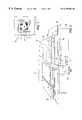
- FIG. 1is a top plan view of a fingerprint sensor in accordance with the present invention.
- FIG. 2is a schematic view of a circuit portion of the fingerprint sensor as shown in FIG. 1 .
- FIG. 3is a greatly enlarged top plan view of the sensing portion of the fingerprint sensor as shown in FIG. 1 .
- FIG. 4is a schematic diagram of another circuit portion of the fingerprint sensor as shown in FIG. 1 .
- FIG. 5is a greatly enlarged side cross-sectional view of a portion of the fingerprint sensor as shown in FIG. 1 .
- FIG. 6is a greatly enlarged side cross-sectional view of a portion of an alternate embodiment of the fingerprint sensor in accordance with the invention.
- FIG. 7is a greatly enlarged side cross-sectional view of another portion of the fingerprint sensor as shown in FIG. 1 .
- FIG. 8is a schematic block diagram of yet another circuit portion of the fingerprint sensor as shown in FIG. 1 .
- FIG. 9is a schematic circuit diagram of a portion of the circuit as shown in FIG. 8 .
- FIG. 10is a schematic block diagram of still another circuit portion of the fingerprint sensor as shown in FIG. 1 .
- FIG. 11is a schematic block diagram of an alternate embodiment of the circuit portion shown in FIG. 10 .
- FIG. 12is a schematic block diagram of an additional circuit portion of the fingerprint sensor as shown in FIG. 1 .
- FIG. 13is a schematic block diagram of an alternate embodiment of the circuit portion shown in FIG. 12 .
- the illustrated sensor 30includes a housing or package 51 , a dielectric layer 52 exposed on an upper surface of the package which provides a placement surface for the finger, and a plurality of output pins, not shown.
- a first conductive strip or external electrode 54 around the periphery of the dielectric layer 52 , and a second external electrode 53provide contact electrodes for the finger 79 as described in greater detail below.
- the sensor 30may provide output signals in a range of sophistication levels depending on the level of processing incorporated in the package as would be readily understood by those skilled in the art.
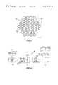
- the sensor 30includes a plurality of individual pixels or sensing elements 30 a arranged in array pattern as perhaps best shown in FIG. 3 .
- these sensing elementsare relatively small so as to be capable of sensing the ridges 59 and intervening valleys 60 of a typical fingerprint.
- live fingerprint readings as from the electric field sensor 30 in accordance with the present inventionmay be more reliable than optical sensing, because the impedance of the skin of a finger in a pattern of ridges and valleys is extremely difficult to simulate.
- an optical sensormay be deceived by a photograph or other similar image of a fingerprint, for example.
- the sensor 30includes a substrate 65 , and one or more active semiconductor devices formed thereon, such as the schematically illustrated amplifier 73 .
- a first metal layer 66interconnects the active semiconductor devices.
- a second or ground plane electrode layer 68is above the first metal layer 66 and separated therefrom by an insulating layer 67 .
- a third metal layer 71is positioned over another dielectric layer 70 .
- the first external electrode 54is connected to an excitation drive amplifier 74 which, in turn, drives the finger 79 with a signal may be typically in the range of about 1 KHz to 1 MHz. Accordingly, the drive or excitation electronics are thus relatively uncomplicated and the overall cost of the sensor 30 may be relatively low, while the reliability is great.
- An illustratively circularly shaped electric field sensing electrode 78is on the insulating layer 70 .
- the sensing electrode 78may be connected to sensing integrated electronics, such as the illustrated amplifier 73 formed adjacent the substrate 65 as schematically illustrated, and as would be readily appreciated by those skilled in the art.
- An annularly shaped shield electrode 80surrounds the sensing electrode 78 in spaced relation therefrom.
- the sensing electrode 78 and its surrounding shield electrode 80may have other shapes, such as hexagonal, for example, to facilitate a close packed arrangement or array of pixels or sensing elements 30 a .
- the shield electrode 80is an active shield which is driven by a portion of the output of the amplifier 73 to help focus the electric field energy and, moreover, to thereby reduce the need to drive adjacent electric field sensing electrodes 78 .
- the sensor 30includes only three metal or electrically conductive layers 66 , 68 and 71 .
- the sensor 30can be made without requiring additional metal layers which would otherwise increase the manufacturing cost, and, perhaps, reduce yields. Accordingly, the sensor 30 is less expensive and may be more rugged and reliable than a sensor including four or more metal layers as would be appreciated by those skilled in the art.
- the amplifier 73may be operated at a gain of greater than about one to drive the shield electrode 80 . Stability problems do not adversely affect the operation of the amplifier 73 . Moreover, the common mode and general noise rejection are greatly enhanced according to this feature of the invention. In addition, the gain greater than one tends to focus the electric field with resect to the sensing electrode 78 as will be readily appreciated by those skilled in the art.
- the sensing elements 30 aoperate at very low currents and at very high impedances.
- the output signal from each sensing electrode 78is desirably about 5 to 10 millivolts to reduce the effects of noise and permit further processing of the signals.
- the approximate diameter of each sensing element 30 aas defined by the outer dimensions of the shield electrode 80 , may be about 0.002 to 0.005 inches in diameter.
- the ground plane electrode 68protects the active electronic devices from unwanted excitation.
- the various signal feedthrough conductors for the electrodes 78 , 80 to the active electronic circuitrymay be readily formed as would be understood by those skilled in the art.
- the overall contact or sensing surface for the sensor 30may desirably be about 0.5 by 0.5 inches—a size which may be readily manufactured and still provide a sufficiently large surface for accurate fingerprint sensing and identification.
- the sensor 30 in accordance with the inventionis also fairly tolerant of dead pixels or sensing elements 30 a .
- a typical sensor 30includes an array of about 256 by 256 pixels or sensor elements, although other array sizes are also contemplated by the present invention.
- the sensor 30may also be fabricated at one time using primarily conventional semiconductor manufacturing techniques to thereby significantly reduce the manufacturing costs.
- the sensormay include power control means for controlling operation of active circuit portions 100 based upon sensing finger contact with the first external electrode 54 as determined by the illustrated finger sense block or circuit 101 .
- the finger sense circuit 101may operate based upon a change in impedance to an oscillator to thereby determine finger contact.
- the power control meansmay include wake-up means for only powering active circuit portions upon sensing finger contact with the first external electrode to thereby conserve power.
- the power control meansmay further comprise protection means for grounding active circuit portions upon not sensing finger contact with the first external electrode. In the illustrated embodiment, a combination of wake-up and protection controller circuits 101 are illustrated.
- the fingerprint sensor 30may further comprise finger charge bleed means for bleeding a charge from a finger or other object upon contact therewith.
- the finger charge bleed meansmay be provided by the second external electrode 53 carried by the package 51 for contact by a finger, and a charge bleed resistor 104 connected between the second external electrode and an earth ground.
- the second electrodemay alternately be provided by a movable electrically conductive cover 53 ′ slidably connected to the package 51 for covering the opening to the exposed upper dielectric layer 52 .
- a pivotally connected coveris also contemplated by the present invention. Accordingly, under normal conditions, the charge would be bled from the finger as the cover 53 ′ is moved to expose the sensing portion of the sensor 30 .
- the finger charge bleed means and power control meansmay be such that the active portions remain grounded until the charge bleed means can remove the charge on the finger before powering the active circuit portions, such as by providing a brief delay during wake-up sufficient to permit the charge to be discharged through the resistor 104 as would be readily understood by those skilled in the art. Accordingly, power may be conserved in the sensor 30 and ESD protection provided by the sensor so that the sensor is relatively inexpensive, yet robust and conserves power.
- the dielectric covering 52may preferably comprise a z-axis anisotropic dielectric layer 110 for focussing an electric field, shown by the illustrated field lines, at each of the electric field sensing electrodes 78 .
- the dielectric layer 110may be relatively thick, but not result in defocussing of the electric fields propagating therethrough because of the z-axis anisotropy of the material.
- a thin film which is desirable for focussingmay permit the underlying circuit to be more easily subject to damage.
- the z-axis anisotropic dielectric layer 110 of the present inventionmay have a thickness in range of about 0.0001 to 0.004 inches.
- the z-axis anisotropic dielectric layer 110is also preferably chemically resistant and mechanically strong to withstand contact with fingers, and to permit periodic cleanings with solvents.
- the z-axis anisotropic dielectric layer 110may preferably define an outermost protective surface for the integrated circuit die 120 .
- the overall dielectric covering 52may further include at least one relatively thin oxide, nitride, carbide, or diamond layer 111 on the integrated circuit die 120 and beneath the z-axis anisotropic dielectric layer 110 .
- the thin layer 111will typically be relatively hard, and the z-axis anisotropic dielectric layer 110 is desirably softer to thereby absorb more mechanical activity.
- the z-axis anisotropic dielectric layer 110may be provided by a plurality of oriented dielectric particles in a cured matrix.
- the z-axis anisotropic dielectric layer 110may comprise barium titanate in a polyimide matrix.
- materials exhibiting z-axis anisotropy suitable for the present inventionFor example, certain ceramics exhibit dielectric anisotropy as would also be appreciated by those skilled in the art.
- FIG. 6another variation of a z-axis dielectric covering 52 ′ is schematically shown by a plurality of high dielectric portions 112 aligned with corresponding electric field sensing electrodes 78 , and a surrounding matrix of lower dielectric portions 113 .
- This embodiment of the dielectric covering 52 ′may be formed in a number of ways, such as by forming a layer of either the high dielectric or low dielectric portions, selectively etching same, and filling the openings with the opposite material. Another approach may be to use polarizable microcapsules and subjecting same to an electric field during curing of a matrix material. A material may be compressed to cause the z-axis anisotropy. Laser and other selective processing techniques may also be used as would be readily understood by those skilled in the art.
- the third metal layer 71(FIG. 2) preferably further includes a plurality of capacitive coupling pads 116 a - 118 a for permitting capacitive coupling of the integrated circuit die 120 .
- the dielectric covering 52is preferably continuous over the capacitive coupling pads 116 a - 118 a and the array of electric field sensing electrodes 78 of the pixels 30 a (FIG. 1 ).
- a portion of the package 51includes a printed circuit board 122 which carries corresponding pads 115 b - 118 b .
- a power modulation circuit 124is coupled to pads 115 b - 116 b
- a signal modulation circuit 126is illustrative coupled to pads 117 b - 118 b .
- both power and signalsmay be readily coupled between the printed circuit board 122 and the integrated circuit die 120 , further using the illustrated power demodulation/regulator circuit 127 , and the signal demodulation circuit 128 .
- the z-axis anisotropic dielectric layer 110also advantageously reduces cross-talk between adjacent capacitive coupling pads.
- This embodiment of the invention 30presents no penetrations through the dielectric covering 52 for moisture to enter and damage the integrated circuit die 120 .
- another level of insulationis provided between the integrated circuit and the external environment.
- the package 51preferably has an opening aligned with the array of electric field sensing electrodes 78 (FIGS. 1 - 3 ).
- the capacitive coupling and z-axis anisotropic layer 110may be advantageously used in a number of applications in addition to the illustrated fingerprint sensor 30 , and particularly where it is desired to have a continuous film covering the upper surface of the integrated circuit die 120 and pads 116 a - 118 a.
- the fingerprint sensor 30may be considered as comprising an array of fingerprint sensing elements 130 and associated active circuits 131 for generating signals relating to the fingerprint image.
- the illustrated sensor 30also includes an impedance matrix 135 connected to the active circuits for filtering the signals therefrom.
- the impedance matrix 135includes a plurality of impedance elements 136 with a respective impedance element connectable between each active circuit of a respective fingerprint sensing element as indicated by the central node 138 , and the other active circuits (outer nodes 140 ).
- the impedance matrix 135also includes a plurality of switches 137 with a respective switch connected in series with each impedance element 136 .
- An input signalmay be supplied to the central node 138 via the illustrated switch 142 and its associated impedance element 143 .
- the impedance elementmay one or more of a resistor as illustrated, and a capacitor 134 as would be readily appreciated by those skilled in the art.
- Filter control meansmay operate the switches 137 to perform processing of the signals generated by the active circuits 131 .
- the fingerprint sensing elements 130may be electric field sensing electrodes 78
- the active circuits 131may be amplifiers 73 (FIG. 2 ).
- other sensing elements and active circuitsmay also benefit from the impedance matrix filtering of the present invention as would be readily understood by those skilled in the art.
- Ridge flow determining means 145may be provided for selectively operating the switches 137 of the matrix 135 to determine ridge flow directions of the fingerprint image. More particularly, the ridge flow determining means 145 may selectively operate the switches 137 for determining signal strength vectors relating to ridge flow directions of the fingerprint image. As would be readily understood by those skilled in the art, the ridge flow directions may be determined based upon well known rotating slit principles.
- the sensor 30may include core location determining means 146 cooperating with the ridge flow determining means 145 for determining a core location of the fingerprint image.
- the position of the coreis helpful, for example, in extracting and processing minutiae from the fingerprint image as would also be readily understood by those skilled in the art.
- a binarizing filter 150may be provided for selectively operating the switches 137 to convert a gray scale fingerprint image to a binarized fingerprint image.
- the impedance matrix 135may be used to provide dynamic image contrast enhancement.
- an edge smoothing filter 155may be readily implemented to improve the image.
- other spatial filters 152may also be implemented using the impedance matrix 135 for selectively operating the switches 137 to spatially filter the fingerprint image as would be readily appreciated by those of skill in the art. Accordingly, processing of the fingerprint image may be carried out at the sensor 30 and thereby reduce additional downstream computational requirements.
- the impedance matrix 135may comprise a plurality of impedance elements with a respective impedance element 136 connectable between each active circuit for a given fingerprint sensing element 130 and eight other active circuits for respective adjacent fingerprint sensing elements.
- control means 153for sequentially powering sets of active circuits 131 to thereby conserve power.
- the respective impedance elements 136are desirably also sequentially connected to perform the filtering function.
- the powered active circuits 131may be considered as defining a cloud or kernel as would be readily appreciated by those skilled in the art.
- the power control means 153may be operated in an adaptive fashion whereby the size of the area used for filtering is dynamically changed for preferred image characteristics as would also be readily understood by those skilled in the art.
- the power control means 153may also power only certain ones of the active circuits corresponding to a predetermined area of the array of sensing elements 130 . For example, every other active circuit 131 could be powered to thereby provide a larger area, but reduced power consumption as would also be understood by those skilled in the art.
- Reader control means 154may be provided to read only predetermined subsets of each set of active circuits 131 so that a contribution from adjacent active circuits is used for filtering.
- only a subset of active circuits 131are typically simultaneously read although adjacent active circuits 131 and associated impedance elements 136 are also powered and connected, respectively.
- 16 impedance elements 136could define a subset and be readily simultaneously read.
- the subset sizecould be optimized for different sized features to be determined as would be readily appreciated by those skilled in the art.
- the array of sense elements 130can be quickly read, and power consumption substantially reduced since all of the active circuits 131 need not be powered for reading a given set of active circuits.
- the combination of the power control and impedance matrix features described hereinmay permit power savings by a factor of about 10 as compared to powering the full array.
- the fingerprint sensor 30It is another important advantage of the fingerprint sensor 30 according to present invention to guard against spoofing or deception of the sensor into incorrectly treating a simulated image as a live fingerprint image.
- optical sensorsmay be deceived or spoofed by using a paper with a fingerprint image thereon.
- the unique electric field sensing of the fingerprint sensor 30 of the present inventionprovides an effective approach to avoiding spoofing based upon the complex impedance of a finger.
- the fingerprint sensor 30may be considered as including an array of impedance sensing elements 160 for generating signals related to a finger 79 or other object positioned adjacent thereto.
- the impedance sensing elements 160are provided by electric field sensing electrodes 78 and amplifiers 73 (FIG. 2) associated therewith.
- a guard shield 80may be associated with each electric field sensing electrode 78 and connected to a respective amplifier 73 .
- Spoof reducing means 161is provided for determining whether or not an impedance of the object positioned adjacent the array of impedance sensing elements 160 corresponds to a live finger 79 to thereby reduce spoofing of the fingerprint sensor by an object other than a live finger.
- a spoofingmay be indicated, such as by the schematically illustrated lamp 163 and/or used to block further processing.
- a live fingerprint determinationmay also be indicated by a lamp 164 and/or used to permit further processing of the fingerprint image as will be readily appreciated by those skilled in the art.
- Many other options for indicating a live fingerprint or an attempted spoofingwill be readily appreciated by those skilled in the art.
- the spoof reducing means 161may include impedance determining means 165 to detect a complex impedance having a phase angle in a range of about 10 to 60 degrees corresponding to a live finger 79 .
- the spoof reducing means 161may detect an impedance having a phase angle of about 0 degrees corresponding to some objects other than a live finger, such as a sheet of paper having an image thereon, for example.
- the spoof reducing means 161may detect an impedance of 90 degrees corresponding to other objects.
- the fingerprint sensor 30may preferably includes drive means for driving the array of impedance sensing elements 160 , such as the illustrated excitation amplifier 74 (FIG. 2 ).
- the sensoralso includes synchronous demodulator means 170 for synchronously demodulating signals from the array of impedance sensing elements 160 .
- the spoof reducing meanscomprises means for operating the synchronous demodulator means 170 at at least one predetermined phase rotation angle.
- the synchronous demodulator means 170could be operated in a range of about 10 to 60 degrees, and the magnitude compared to a predetermined threshold indicative of a live fingerprint.
- a live fingerprinttypically has a complex impedance within the range of 10 to 60 degrees.
- ratio generating and comparing means 172may be provided for cooperating with the synchronous demodulator means 170 for synchronously demodulating signals at first and second phase angles ⁇ 1 , ⁇ 2 , generating an amplitude ratio thereof, and comparing the amplitude ratio to a predetermined threshold to determine whether the object is a live fingerprint or other object.
- the synchronous demodulator 170may be readily used to generate the impedance information desired for reducing spoofing of the sensor 30 by an object other than a live finger.
- the first angle ⁇ 1 and the second ⁇ 2may have a difference in a range of about 45 to 90 degrees, for example. Other angles are also contemplated by the invention as would be readily appreciated by those skilled in the art.
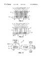
- the fingerprint sensor 30also includes an automatic gain control feature to account for a difference in intensity of the image signals generated by different fingers or under different conditions, and also to account for differences in sensor caused by process variations. It is important for accurately producing a fingerprint image, that the sensor can discriminate between the ridges and valleys of the fingerprint. Accordingly, the sensor 30 includes a gain control feature, a first embodiment of which is understood with reference to FIG. 12 .
- the illustrated portion of the fingerprint sensor 30includes an array of fingerprint sensing elements in the form of the electric field sensing electrodes 78 and surrounding shield electrodes 80 connected to the amplifiers 73 .
- Other fingerprint sensing elementsmay also benefit from the following automatic gain control implementations as will be appreciated by those skilled in the art.
- the signal processing circuitry of the sensor 30preferably includes a plurality of analog-to-digital (A/D) converters 180 as illustrated. Moreover, each of these A/D converters 180 may have a controllable scale. Scanning means 182 sequentially connects different elements to the bank of A/D converters 180 .
- the illustrated gain processor 185provides range determining and setting means for controlling the range of the A/D converters 180 based upon prior A/D conversions to thereby provide enhanced conversion resolution.
- the A/D converters 180may comprise the illustrated reference voltage input V ref and offset voltage input V offset for permitting setting of the range as would be readily appreciated by those skilled in the at.
- the range determining and setting meansmay also comprise a first digital-to-analog D/A converter 186 connected between the gain processor 185 and the reference voltage V ref inputs of the A/D converters 180 as would also be readily understood by those skilled in the art.
- a second D/A converter 189is also illustratively connected to the offset voltage inputs V offset from the gain processor 185 .
- the gain processor 185may comprise histogram generating means for generating a histogram, as described above, and based upon prior A/D conversions.
- the graph adjacent the gain processor 185 in FIG. 12illustrates a typical histogram plot 191 .
- the histogram plot 191includes two peaks corresponding to the sensed ridges and valleys of the fingerprint as would be readily appreciated by those skilled in the art. By setting the range for the A/D converters 180 , the peaks can be readily positioned as desired to thereby account for the variations discussed above and use the full resolution of the A/D converters 180 .
- the A/D converters 180may include an associated input amplifier for permitting setting of the range.
- the range determining and setting meansmay also comprise the illustrated gain processor 185 , and wherein the amplifier is a programmable gain amplifier (PGA) 187 connected to the processor.
- PGAprogrammable gain amplifier
- a digital word output from the gain processor 185sets the gain of the PGA 187 so that full use of the resolution of the A/D converters 180 is obtained for best accuracy.
- a second digital word output from the gain processor 185 and coupled to the amplifier 187 through the illustrated D/A converter 192may also control the offset of the amplifier as would also be readily appreciated by those skilled in the art.
- the range determining and setting means of the gain processor 185may comprise default setting means for setting a default range for initial ones of the fingerprint sensing elements.
- the automatic gain control feature of the present inventionallows the D/A converters 180 to operate over their full resolution range to thereby increase the accuracy of the image signal processing.
Landscapes
- Engineering & Computer Science (AREA)
- Human Computer Interaction (AREA)
- Physics & Mathematics (AREA)
- General Physics & Mathematics (AREA)
- Multimedia (AREA)
- Theoretical Computer Science (AREA)
- Image Input (AREA)
- Measurement Of Length, Angles, Or The Like Using Electric Or Magnetic Means (AREA)
- Measurement Of The Respiration, Hearing Ability, Form, And Blood Characteristics Of Living Organisms (AREA)
Abstract
Description
Claims (26)
Priority Applications (8)
| Application Number | Priority Date | Filing Date | Title |
|---|---|---|---|
| US08/858,142US6259804B1 (en) | 1997-05-16 | 1997-05-16 | Fingerprint sensor with gain control features and associated methods |
| JP54930298AJP4129892B2 (en) | 1997-05-16 | 1998-05-06 | Fingerprint sensor having gain control configuration and related method |
| EP98921014AEP0985196B9 (en) | 1997-05-16 | 1998-05-06 | Fingerprint sensor with gain control features and associated methods |
| CN98806249ACN1290383A (en) | 1997-05-16 | 1998-05-06 | Fingerprint sensor with gain control features and associated methods |
| DE69809907TDE69809907T2 (en) | 1997-05-16 | 1998-05-06 | FINGERPRINT SENSOR WITH GAIN CONTROL FEATURES AND RELATED METHODS |
| KR1019997010596AKR20010012635A (en) | 1997-05-16 | 1998-05-06 | Fingerprint sensor with gain control features and associated methods |
| PCT/US1998/009292WO1998052157A1 (en) | 1997-05-16 | 1998-05-06 | Fingerprint sensor with gain control features and associated methods |
| AU73715/98AAU7371598A (en) | 1997-05-16 | 1998-05-06 | Fingerprint sensor with gain control features and associated methods |
Applications Claiming Priority (1)
| Application Number | Priority Date | Filing Date | Title |
|---|---|---|---|
| US08/858,142US6259804B1 (en) | 1997-05-16 | 1997-05-16 | Fingerprint sensor with gain control features and associated methods |
Publications (1)
| Publication Number | Publication Date |
|---|---|
| US6259804B1true US6259804B1 (en) | 2001-07-10 |
Family
ID=25327595
Family Applications (1)
| Application Number | Title | Priority Date | Filing Date |
|---|---|---|---|
| US08/858,142Expired - LifetimeUS6259804B1 (en) | 1997-05-16 | 1997-05-16 | Fingerprint sensor with gain control features and associated methods |
Country Status (8)
| Country | Link |
|---|---|
| US (1) | US6259804B1 (en) |
| EP (1) | EP0985196B9 (en) |
| JP (1) | JP4129892B2 (en) |
| KR (1) | KR20010012635A (en) |
| CN (1) | CN1290383A (en) |
| AU (1) | AU7371598A (en) |
| DE (1) | DE69809907T2 (en) |
| WO (1) | WO1998052157A1 (en) |
Cited By (80)
| Publication number | Priority date | Publication date | Assignee | Title |
|---|---|---|---|---|
| US20020146156A1 (en)* | 2000-12-15 | 2002-10-10 | Hiroki Morimura | Image capturing method and apparatus and fingerprint collation method and apparatus |
| US20030013328A1 (en)* | 2001-05-22 | 2003-01-16 | Andrade Thomas L. | Connection assembly for integrated circuit sensors |
| US20030020495A1 (en)* | 2001-05-22 | 2003-01-30 | Andrade Thomas L. | Surface capacitance sensor system using buried stimulus electrode |
| US6518560B1 (en)* | 2000-04-27 | 2003-02-11 | Veridicom, Inc. | Automatic gain amplifier for biometric sensor device |
| US6556935B2 (en)* | 2000-06-08 | 2003-04-29 | Nippon Telegraph And Telephone Corporation | Small shape recognizing capacitive sensor device |
| US6611614B1 (en)* | 1997-12-18 | 2003-08-26 | Infineon Technologies Ag | Image acquisition apparatus |
| US6631579B1 (en)* | 1998-03-12 | 2003-10-14 | Peter Lauster | Detent for a handgun |
| US6647133B1 (en)* | 1998-12-10 | 2003-11-11 | Omron Corporation | Fingerprint identification device-equip with a touch sensor for detecting a human finger |
| US20030210809A1 (en)* | 2002-05-07 | 2003-11-13 | Wonchan Kim | Apparatus and method for sensing the degree and touch strength of a human body on a sensor |
| US6665428B1 (en)* | 2000-08-28 | 2003-12-16 | Stmicroelectronics, Inc. | Resistive finger detection for fingerprint sensor |
| US20040001018A1 (en)* | 2002-06-05 | 2004-01-01 | Hales Rex K. | Analog-to-digital converter with digital signal processing functionality to emulate many different sample frequencies, resolutions, and architectures |
| US20040033086A1 (en)* | 2002-08-15 | 2004-02-19 | Vejtasa David S. | System and method for recycling hydrocarbon-based carrier liquid |
| US20040078101A1 (en)* | 2002-03-27 | 2004-04-22 | Kabushiki Kaisha Toshiba | Plant protective instrumentation equipment |
| US20040156538A1 (en)* | 2001-03-06 | 2004-08-12 | Manfred Greschitz | Fingerprint sensor with potential modulation of the ESD protective grating |
| US20050010787A1 (en)* | 1999-04-30 | 2005-01-13 | Microvision, Inc. | Method and system for identifying data locations associated with real world observations |
| US20050012714A1 (en)* | 2003-06-25 | 2005-01-20 | Russo Anthony P. | System and method for a miniature user input device |
| US20050041885A1 (en)* | 2003-08-22 | 2005-02-24 | Russo Anthony P. | System for and method of generating rotational inputs |
| US20050078855A1 (en)* | 2003-10-10 | 2005-04-14 | Authentec Inc. State Of Incorporation: Delaware | Electronic device including fingerprint sensor and display having selectable menu items and associated methods |
| WO2005055429A1 (en) | 2003-12-02 | 2005-06-16 | Giesecke & Devrient Gmbh | Digitizing a papillary structure |
| US20050169503A1 (en)* | 2004-01-29 | 2005-08-04 | Howell Mark J. | System for and method of finger initiated actions |
| US20050179657A1 (en)* | 2004-02-12 | 2005-08-18 | Atrua Technologies, Inc. | System and method of emulating mouse operations using finger image sensors |
| US20050220329A1 (en)* | 2004-03-31 | 2005-10-06 | Seiko Epson Corporation | Method of focusing a fingerprint image and a fingerprint sensing device |
| US7020308B1 (en)* | 1999-09-14 | 2006-03-28 | Fujitsu Limited | Personal authentication system using biometrics information |
| US20060078174A1 (en)* | 2004-10-08 | 2006-04-13 | Atrua Technologies, Inc. | System for and method of determining pressure on a finger sensor |
| US20060103633A1 (en)* | 2004-11-17 | 2006-05-18 | Atrua Technologies, Inc. | Customizable touch input module for an electronic device |
| US20060140456A1 (en)* | 2002-12-20 | 2006-06-29 | Fondeur Jean-Christophe | Method of determining the living character of an element carrying a fingerprint |
| US20060182319A1 (en)* | 2005-02-17 | 2006-08-17 | Authentec, Inc. | Finger sensor apparatus using image resampling and associated methods |
| US20060181521A1 (en)* | 2005-02-14 | 2006-08-17 | Atrua Technologies, Inc. | Systems for dynamically illuminating touch sensors |
| US7139414B1 (en)* | 1999-06-24 | 2006-11-21 | Nec Corporation | Method for removing static electricity in fingerprint-reading apparatus, fingerprint reading apparatus and data terminal provided with fingerprint-reading apparatus |
| US20070014443A1 (en)* | 2005-07-12 | 2007-01-18 | Anthony Russo | System for and method of securing fingerprint biometric systems against fake-finger spoofing |
| US20070086634A1 (en)* | 2005-10-18 | 2007-04-19 | Authentec, Inc. | Finger sensor including enhanced esd protection and associated methods |
| US20070098228A1 (en)* | 2005-11-01 | 2007-05-03 | Atrua Technologies, Inc | Devices using a metal layer with an array of vias to reduce degradation |
| US7256589B2 (en) | 2001-04-27 | 2007-08-14 | Atrua Technologies, Inc. | Capacitive sensor system with improved capacitance measuring sensitivity |
| US20070207681A1 (en)* | 2005-04-08 | 2007-09-06 | Atrua Technologies, Inc. | System for and method of protecting an integrated circuit from over currents |
| US20070253606A1 (en)* | 2006-04-28 | 2007-11-01 | Nec Corporation | Image reading apparatus for feature image of live body |
| US20070253607A1 (en)* | 2006-04-28 | 2007-11-01 | Nec Corporation | Image reading apparatus for feature image of live body |
| US20080013808A1 (en)* | 2006-07-13 | 2008-01-17 | Russo Anthony P | System for and method of assigning confidence values to fingerprint minutiae points |
| US20080030207A1 (en)* | 2000-06-09 | 2008-02-07 | Idex Asa | Miniature sensor chip, especially for finger print sensors |
| US20080317300A1 (en)* | 2007-06-22 | 2008-12-25 | Mstar Semiconductor, Inc. | Fingerprint Sensing Circuit |
| US7565541B1 (en)* | 2000-06-21 | 2009-07-21 | Microvision, Inc. | Digital fingerprint identification system |
| US20090257626A1 (en)* | 2005-10-18 | 2009-10-15 | Authentec, Inc. | Thinned finger sensor and associated methods |
| US20100119125A1 (en)* | 2008-11-12 | 2010-05-13 | Chi Mei Communication Systems, Inc. | Fingerprint identification system and method of an electronic device |
| US7831070B1 (en) | 2005-02-18 | 2010-11-09 | Authentec, Inc. | Dynamic finger detection mechanism for a fingerprint sensor |
| US20110025835A1 (en)* | 2004-11-15 | 2011-02-03 | Nec Corporation | Apparatus for Inputing Biometrical Feature |
| US20110253785A1 (en)* | 2010-03-30 | 2011-10-20 | Willie Anthony Johnson | Multi-Pass Biometric Scanner |
| US8074086B1 (en)* | 2006-12-11 | 2011-12-06 | Cypress Semiconductor Corporation | Circuit and method for dynamic in-rush current control in a power management circuit |
| WO2011160014A1 (en) | 2010-06-18 | 2011-12-22 | Authentec, Inc. | Finger sensor including encapsulating layer over sensing area and related methods |
| WO2012061559A1 (en) | 2010-11-05 | 2012-05-10 | Authentec, Inc. | Method of making a finger sensor package and associated devices |
| US8421890B2 (en) | 2010-01-15 | 2013-04-16 | Picofield Technologies, Inc. | Electronic imager using an impedance sensor grid array and method of making |
| US8495431B2 (en)* | 2008-06-26 | 2013-07-23 | International Business Machines Corporation | Temperature-profiled device fingerprint generation and authentication from power-up states of static cells |
| US8558811B2 (en) | 2005-11-15 | 2013-10-15 | Synaptics Incorporated | Methods and systems for detecting a position-based attribute of an object using digital codes |
| US20130271422A1 (en)* | 2012-04-13 | 2013-10-17 | Apple Inc. | Capacitive Sensing Array Modulation |
| US8724038B2 (en) | 2010-10-18 | 2014-05-13 | Qualcomm Mems Technologies, Inc. | Wraparound assembly for combination touch, handwriting and fingerprint sensor |
| US8730204B2 (en) | 2010-09-16 | 2014-05-20 | Synaptics Incorporated | Systems and methods for signaling and interference detection in sensor devices |
| US8743080B2 (en) | 2011-06-27 | 2014-06-03 | Synaptics Incorporated | System and method for signaling in sensor devices |
| US8766949B2 (en) | 2011-12-22 | 2014-07-01 | Synaptics Incorporated | Systems and methods for determining user input using simultaneous transmission from multiple electrodes |
| US8791792B2 (en) | 2010-01-15 | 2014-07-29 | Idex Asa | Electronic imager using an impedance sensor grid array mounted on or about a switch and method of making |
| US8866347B2 (en) | 2010-01-15 | 2014-10-21 | Idex Asa | Biometric image sensing |
| US9001081B2 (en) | 2012-05-18 | 2015-04-07 | Apple Inc. | Capacitive sensor packaging |
| US9024910B2 (en) | 2012-04-23 | 2015-05-05 | Qualcomm Mems Technologies, Inc. | Touchscreen with bridged force-sensitive resistors |
| US9063608B2 (en) | 2012-06-14 | 2015-06-23 | Synaptics Incorporated | Systems and methods for sensor devices having a non-commensurate number of transmitter electrodes |
| US9176633B2 (en) | 2014-03-31 | 2015-11-03 | Synaptics Incorporated | Sensor device and method for estimating noise in a capacitive sensing device |
| CN105404880A (en)* | 2015-12-25 | 2016-03-16 | 成都费恩格尔微电子技术有限公司 | Electronic device with fingerprint sensor assembly |
| US9305959B2 (en) | 2013-06-05 | 2016-04-05 | Apple Inc. | Biometric sensor chip having distributed sensor and control circuitry |
| US9460332B1 (en) | 2013-09-09 | 2016-10-04 | Apple Inc. | Capacitive fingerprint sensor including an electrostatic lens |
| US20170024601A1 (en)* | 2015-07-22 | 2017-01-26 | Egalax_Empia Technology Inc. | Biometric identification apparatus |
| WO2017091663A1 (en)* | 2015-11-23 | 2017-06-01 | Jensen Eric Dean | Fingerprint reader |
| US9672403B2 (en) | 2014-09-16 | 2017-06-06 | Fingerprint Cards Ab | Method and fingerprint sensing system for authenticating a candidate fingerprint |
| US9697409B2 (en) | 2013-09-10 | 2017-07-04 | Apple Inc. | Biometric sensor stack structure |
| US9721139B2 (en) | 2014-08-29 | 2017-08-01 | Samsung Electronics Co., Ltd. | Fingerprint detection sensor and fingerprint detection system comprising the same |
| US9798917B2 (en) | 2012-04-10 | 2017-10-24 | Idex Asa | Biometric sensing |
| EP3252659A1 (en)* | 2016-05-30 | 2017-12-06 | Guangdong Oppo Mobile Telecommunications Corp., Ltd. | Method for controlling unlocking an terminal |
| US9883822B2 (en) | 2013-06-05 | 2018-02-06 | Apple Inc. | Biometric sensor chip having distributed sensor and control circuitry |
| US20180039809A1 (en)* | 2016-08-02 | 2018-02-08 | Samsung Electronics Co., Ltd. | Analog front end circuit for use with fingerprint sensor, and device having the same |
| US9984270B2 (en) | 2013-08-05 | 2018-05-29 | Apple Inc. | Fingerprint sensor in an electronic device |
| US10019122B2 (en) | 2016-03-31 | 2018-07-10 | Synaptics Incorporated | Capacitive sensing using non-integer excitation |
| US10025428B2 (en) | 2015-11-19 | 2018-07-17 | Synaptics Incorporated | Method and apparatus for improving capacitive sensing detection |
| US20190087628A1 (en)* | 2017-09-15 | 2019-03-21 | Samsung Display Co., Ltd. | Biometric information detecting device and display apparatus having the same |
| US10296773B2 (en) | 2013-09-09 | 2019-05-21 | Apple Inc. | Capacitive sensing array having electrical isolation |
| US10762321B2 (en) | 2016-07-04 | 2020-09-01 | Truly (Huizhou) Smart Display Limited | Fingerprint recognition unit circuit, control method therefor, and fingerprint recognition apparatus |
Families Citing this family (15)
| Publication number | Priority date | Publication date | Assignee | Title |
|---|---|---|---|---|
| DE19901384A1 (en)* | 1999-01-15 | 2000-07-27 | Siemens Ag | Electronic component and use of a protective structure contained therein |
| DE50011685D1 (en)* | 2000-04-14 | 2005-12-29 | Infineon Technologies Ag | Capacitive biometric sensor |
| NO314647B1 (en)* | 2000-06-09 | 2003-04-22 | Idex Asa | Fingerprint sensor measurement system |
| NO315017B1 (en)* | 2000-06-09 | 2003-06-23 | Idex Asa | Sensor chip, especially for measuring structures in a finger surface |
| KR20060038274A (en)* | 2004-10-29 | 2006-05-03 | 엘지전자 주식회사 | Fingerprint sensor and fingerprint recognition device of mobile communication terminal using same |
| US8805031B2 (en)* | 2008-05-08 | 2014-08-12 | Sonavation, Inc. | Method and system for acoustic impediography biometric sensing |
| NO20131423A1 (en) | 2013-02-22 | 2014-08-25 | Idex Asa | Integrated fingerprint sensor |
| CN106575351B (en) | 2014-02-21 | 2019-12-13 | 傲迪司威生物识别公司 | Sensor employing overlapping grid lines and conductive probes for extending a sensing surface from the grid lines |
| KR101613123B1 (en)* | 2014-04-10 | 2016-04-18 | 크루셜텍 (주) | Fingerprint detecting apparatuse and driving signal attenuation compensation method |
| CN104252621A (en)* | 2014-09-29 | 2014-12-31 | 深圳市汇顶科技股份有限公司 | Fingerprint identification device and fingerprint identification method |
| TWI580973B (en)* | 2015-11-10 | 2017-05-01 | Chroma Ate Inc | A global detection method of fingerprint sensor and its testing equipment |
| CN105913049B (en)* | 2016-03-31 | 2020-04-10 | 深圳市奔凯安全技术股份有限公司 | Fingerprint acquisition device |
| CN107657694B (en)* | 2017-09-13 | 2020-01-14 | 深圳市无线道科技有限公司 | Fingerprint identification circuit of remote anti-theft door |
| CN107633579B (en)* | 2017-09-13 | 2020-05-01 | 洪菲菲 | Fingerprint identification circuit of anti-theft door |
| CN107492178B (en)* | 2017-09-13 | 2020-01-07 | 伦燕宽 | Fingerprint control circuit of remote anti-theft door |
Citations (36)
| Publication number | Priority date | Publication date | Assignee | Title |
|---|---|---|---|---|
| US3781672A (en)* | 1971-05-10 | 1973-12-25 | Drexelbrook Controls | Continuous condition measuring system |
| US4202120A (en) | 1978-04-10 | 1980-05-13 | Engel Elton D | Identification card, sensor, and system |
| US4210899A (en) | 1975-06-23 | 1980-07-01 | Fingermatrix, Inc. | Fingerprint-based access control and identification apparatus |
| US4353056A (en)* | 1980-06-05 | 1982-10-05 | Siemens Corporation | Capacitive fingerprint sensor |
| US4557504A (en) | 1983-01-17 | 1985-12-10 | Kuhns Roger J | Method for thwarting forgery of fingerprint-bearing identification media |
| WO1986006527A1 (en) | 1985-04-22 | 1986-11-06 | The Quantum Fund Ltd. | Skin-pattern recognition method and device |
| US4768021A (en) | 1987-09-18 | 1988-08-30 | Ferraro Michael P | Safe for loaded hand gun |
| DE3712089A1 (en) | 1987-04-09 | 1988-10-27 | Jaspal Singh | Arrangement for identifying the papillary line pattern of a finger |
| US4811414A (en) | 1987-02-27 | 1989-03-07 | C.F.A. Technologies, Inc. | Methods for digitally noise averaging and illumination equalizing fingerprint images |
| US4827191A (en)* | 1987-09-08 | 1989-05-02 | Motorola, Inc. | Adaptive range/DC restoration circuit or use with analog to digital convertors |
| JPH01146464A (en) | 1987-12-03 | 1989-06-08 | Oki Electric Ind Co Ltd | Agc circuit in picture reader |
| JPH0231377A (en) | 1988-07-21 | 1990-02-01 | Ricoh Co Ltd | Auto level control device for audio recording and playback equipment |
| US4983846A (en) | 1989-08-22 | 1991-01-08 | Arturo M. Rios | Portable fingerprint detection method and device |
| US4993068A (en) | 1989-11-27 | 1991-02-12 | Motorola, Inc. | Unforgeable personal identification system |
| US5222152A (en) | 1991-11-19 | 1993-06-22 | Digital Biometrics, Inc. | Portable fingerprint scanning apparatus for identification verification |
| US5224173A (en) | 1991-10-29 | 1993-06-29 | Kuhns Roger J | Method of reducing fraud in connection with employment, public license applications, social security, food stamps, welfare or other government benefits |
| US5245329A (en) | 1989-02-27 | 1993-09-14 | Security People Inc. | Access control system with mechanical keys which store data |
| US5280527A (en) | 1992-04-14 | 1994-01-18 | Kamahira Safe Co., Inc. | Biometric token for authorizing access to a host system |
| US5325442A (en) | 1990-05-18 | 1994-06-28 | U.S. Philips Corporation | Fingerprint sensing device and recognition system having predetermined electrode activation |
| US5363453A (en) | 1989-11-02 | 1994-11-08 | Tms Inc. | Non-minutiae automatic fingerprint identification system and methods |
| US5386104A (en) | 1993-11-08 | 1995-01-31 | Ncr Corporation | System and method for detecting user fraud in automated teller machine transactions |
| US5389927A (en)* | 1993-05-28 | 1995-02-14 | Motorola, Inc. | Method and apparatus for control of an analog to digital converter |
| US5461425A (en)* | 1994-02-15 | 1995-10-24 | Stanford University | CMOS image sensor with pixel level A/D conversion |
| US5467403A (en) | 1991-11-19 | 1995-11-14 | Digital Biometrics, Inc. | Portable fingerprint scanning apparatus for identification verification |
| US5509083A (en) | 1994-06-15 | 1996-04-16 | Nooral S. Abtahi | Method and apparatus for confirming the identity of an individual presenting an identification card |
| US5513272A (en) | 1994-12-05 | 1996-04-30 | Wizards, Llc | System for verifying use of a credit/identification card including recording of physical attributes of unauthorized users |
| US5541994A (en) | 1994-09-07 | 1996-07-30 | Mytec Technologies Inc. | Fingerprint controlled public key cryptographic system |
| US5546471A (en) | 1994-10-28 | 1996-08-13 | The National Registry, Inc. | Ergonomic fingerprint reader apparatus |
| US5598474A (en) | 1994-03-29 | 1997-01-28 | Neldon P Johnson | Process for encrypting a fingerprint onto an I.D. card |
| US5603179A (en) | 1995-10-11 | 1997-02-18 | Adams; Heiko B. | Safety trigger |
| US5613712A (en) | 1995-04-21 | 1997-03-25 | Eastman Kodak Company | Magnetic fingerprint for secure document authentication |
| US5623552A (en) | 1994-01-21 | 1997-04-22 | Cardguard International, Inc. | Self-authenticating identification card with fingerprint identification |
| EP0786745A2 (en) | 1996-01-26 | 1997-07-30 | Harris Corporation | Enhanced security fingerprint sensor package and related methods |
| US5778089A (en)* | 1996-03-04 | 1998-07-07 | Dew Engineering And Development Limited | Driver circuit for a contact imaging array |
| US5828773A (en)* | 1996-01-26 | 1998-10-27 | Harris Corporation | Fingerprint sensing method with finger position indication |
| US6023522A (en)* | 1997-05-05 | 2000-02-08 | Draganoff; Georgi H. | Inexpensive adaptive fingerprint image acquisition framegrabber |
Family Cites Families (1)
| Publication number | Priority date | Publication date | Assignee | Title |
|---|---|---|---|---|
| US4525859A (en) | 1982-09-03 | 1985-06-25 | Bowles Romald E | Pattern recognition system |
- 1997
- 1997-05-16USUS08/858,142patent/US6259804B1/ennot_activeExpired - Lifetime
- 1998
- 1998-05-06JPJP54930298Apatent/JP4129892B2/ennot_activeExpired - Lifetime
- 1998-05-06KRKR1019997010596Apatent/KR20010012635A/ennot_activeWithdrawn
- 1998-05-06EPEP98921014Apatent/EP0985196B9/ennot_activeExpired - Lifetime
- 1998-05-06DEDE69809907Tpatent/DE69809907T2/ennot_activeExpired - Lifetime
- 1998-05-06AUAU73715/98Apatent/AU7371598A/ennot_activeAbandoned
- 1998-05-06WOPCT/US1998/009292patent/WO1998052157A1/ennot_activeApplication Discontinuation
- 1998-05-06CNCN98806249Apatent/CN1290383A/enactivePending
Patent Citations (37)
| Publication number | Priority date | Publication date | Assignee | Title |
|---|---|---|---|---|
| US3781672A (en)* | 1971-05-10 | 1973-12-25 | Drexelbrook Controls | Continuous condition measuring system |
| US4210899A (en) | 1975-06-23 | 1980-07-01 | Fingermatrix, Inc. | Fingerprint-based access control and identification apparatus |
| US4202120A (en) | 1978-04-10 | 1980-05-13 | Engel Elton D | Identification card, sensor, and system |
| US4353056A (en)* | 1980-06-05 | 1982-10-05 | Siemens Corporation | Capacitive fingerprint sensor |
| US4557504A (en) | 1983-01-17 | 1985-12-10 | Kuhns Roger J | Method for thwarting forgery of fingerprint-bearing identification media |
| WO1986006527A1 (en) | 1985-04-22 | 1986-11-06 | The Quantum Fund Ltd. | Skin-pattern recognition method and device |
| US4811414A (en) | 1987-02-27 | 1989-03-07 | C.F.A. Technologies, Inc. | Methods for digitally noise averaging and illumination equalizing fingerprint images |
| DE3712089A1 (en) | 1987-04-09 | 1988-10-27 | Jaspal Singh | Arrangement for identifying the papillary line pattern of a finger |
| US4827191A (en)* | 1987-09-08 | 1989-05-02 | Motorola, Inc. | Adaptive range/DC restoration circuit or use with analog to digital convertors |
| US4768021A (en) | 1987-09-18 | 1988-08-30 | Ferraro Michael P | Safe for loaded hand gun |
| US4768021C1 (en) | 1987-09-18 | 2002-07-23 | Jmf Products Llc | Safe for loaded hand gun |
| JPH01146464A (en) | 1987-12-03 | 1989-06-08 | Oki Electric Ind Co Ltd | Agc circuit in picture reader |
| JPH0231377A (en) | 1988-07-21 | 1990-02-01 | Ricoh Co Ltd | Auto level control device for audio recording and playback equipment |
| US5245329A (en) | 1989-02-27 | 1993-09-14 | Security People Inc. | Access control system with mechanical keys which store data |
| US4983846A (en) | 1989-08-22 | 1991-01-08 | Arturo M. Rios | Portable fingerprint detection method and device |
| US5363453A (en) | 1989-11-02 | 1994-11-08 | Tms Inc. | Non-minutiae automatic fingerprint identification system and methods |
| US4993068A (en) | 1989-11-27 | 1991-02-12 | Motorola, Inc. | Unforgeable personal identification system |
| US5325442A (en) | 1990-05-18 | 1994-06-28 | U.S. Philips Corporation | Fingerprint sensing device and recognition system having predetermined electrode activation |
| US5224173A (en) | 1991-10-29 | 1993-06-29 | Kuhns Roger J | Method of reducing fraud in connection with employment, public license applications, social security, food stamps, welfare or other government benefits |
| US5467403A (en) | 1991-11-19 | 1995-11-14 | Digital Biometrics, Inc. | Portable fingerprint scanning apparatus for identification verification |
| US5222152A (en) | 1991-11-19 | 1993-06-22 | Digital Biometrics, Inc. | Portable fingerprint scanning apparatus for identification verification |
| US5280527A (en) | 1992-04-14 | 1994-01-18 | Kamahira Safe Co., Inc. | Biometric token for authorizing access to a host system |
| US5389927A (en)* | 1993-05-28 | 1995-02-14 | Motorola, Inc. | Method and apparatus for control of an analog to digital converter |
| US5386104A (en) | 1993-11-08 | 1995-01-31 | Ncr Corporation | System and method for detecting user fraud in automated teller machine transactions |
| US5623552A (en) | 1994-01-21 | 1997-04-22 | Cardguard International, Inc. | Self-authenticating identification card with fingerprint identification |
| US5461425A (en)* | 1994-02-15 | 1995-10-24 | Stanford University | CMOS image sensor with pixel level A/D conversion |
| US5598474A (en) | 1994-03-29 | 1997-01-28 | Neldon P Johnson | Process for encrypting a fingerprint onto an I.D. card |
| US5509083A (en) | 1994-06-15 | 1996-04-16 | Nooral S. Abtahi | Method and apparatus for confirming the identity of an individual presenting an identification card |
| US5541994A (en) | 1994-09-07 | 1996-07-30 | Mytec Technologies Inc. | Fingerprint controlled public key cryptographic system |
| US5546471A (en) | 1994-10-28 | 1996-08-13 | The National Registry, Inc. | Ergonomic fingerprint reader apparatus |
| US5513272A (en) | 1994-12-05 | 1996-04-30 | Wizards, Llc | System for verifying use of a credit/identification card including recording of physical attributes of unauthorized users |
| US5613712A (en) | 1995-04-21 | 1997-03-25 | Eastman Kodak Company | Magnetic fingerprint for secure document authentication |
| US5603179A (en) | 1995-10-11 | 1997-02-18 | Adams; Heiko B. | Safety trigger |
| EP0786745A2 (en) | 1996-01-26 | 1997-07-30 | Harris Corporation | Enhanced security fingerprint sensor package and related methods |
| US5828773A (en)* | 1996-01-26 | 1998-10-27 | Harris Corporation | Fingerprint sensing method with finger position indication |
| US5778089A (en)* | 1996-03-04 | 1998-07-07 | Dew Engineering And Development Limited | Driver circuit for a contact imaging array |
| US6023522A (en)* | 1997-05-05 | 2000-02-08 | Draganoff; Georgi H. | Inexpensive adaptive fingerprint image acquisition framegrabber |
Non-Patent Citations (2)
| Title |
|---|
| Patent Abstracts of Japan, vol. 013, No. 407 (E-818), Sep. 8, 1989 & JP 01 146464 A (Oki Electric Ind Co). |
| Patent Abstracts of Japan, vol. 014, No. 185 (P-1036), Apr. 13, 1990 & JP 02 031377 A (Ricoh Co Ltd). |
Cited By (155)
| Publication number | Priority date | Publication date | Assignee | Title |
|---|---|---|---|---|
| US6611614B1 (en)* | 1997-12-18 | 2003-08-26 | Infineon Technologies Ag | Image acquisition apparatus |
| US6631579B1 (en)* | 1998-03-12 | 2003-10-14 | Peter Lauster | Detent for a handgun |
| US6647133B1 (en)* | 1998-12-10 | 2003-11-11 | Omron Corporation | Fingerprint identification device-equip with a touch sensor for detecting a human finger |
| US20050010787A1 (en)* | 1999-04-30 | 2005-01-13 | Microvision, Inc. | Method and system for identifying data locations associated with real world observations |
| US7139414B1 (en)* | 1999-06-24 | 2006-11-21 | Nec Corporation | Method for removing static electricity in fingerprint-reading apparatus, fingerprint reading apparatus and data terminal provided with fingerprint-reading apparatus |
| US7020308B1 (en)* | 1999-09-14 | 2006-03-28 | Fujitsu Limited | Personal authentication system using biometrics information |
| US20060120577A1 (en)* | 1999-09-14 | 2006-06-08 | Fujitsu Limited | Personal authentication system using biometrics information |
| US7974448B2 (en) | 1999-09-14 | 2011-07-05 | Fujitsu Limted | Personal authentication system using biometrics information |
| US6518560B1 (en)* | 2000-04-27 | 2003-02-11 | Veridicom, Inc. | Automatic gain amplifier for biometric sensor device |
| US6556935B2 (en)* | 2000-06-08 | 2003-04-29 | Nippon Telegraph And Telephone Corporation | Small shape recognizing capacitive sensor device |
| US7518382B2 (en)* | 2000-06-09 | 2009-04-14 | Idex Asa | Miniature sensor chip, especially for finger print sensors |
| US20080030207A1 (en)* | 2000-06-09 | 2008-02-07 | Idex Asa | Miniature sensor chip, especially for finger print sensors |
| US7565541B1 (en)* | 2000-06-21 | 2009-07-21 | Microvision, Inc. | Digital fingerprint identification system |
| US6665428B1 (en)* | 2000-08-28 | 2003-12-16 | Stmicroelectronics, Inc. | Resistive finger detection for fingerprint sensor |
| US20020146156A1 (en)* | 2000-12-15 | 2002-10-10 | Hiroki Morimura | Image capturing method and apparatus and fingerprint collation method and apparatus |
| US6990219B2 (en)* | 2000-12-15 | 2006-01-24 | Nippon Telegraph And Telephone Corporation | Image capturing method and apparatus and fingerprint collation method and apparatus |
| US20040156538A1 (en)* | 2001-03-06 | 2004-08-12 | Manfred Greschitz | Fingerprint sensor with potential modulation of the ESD protective grating |
| US7027625B2 (en)* | 2001-03-06 | 2006-04-11 | Infineon Technologies Ag | Fingerprint sensor with potential modulation of the ESD protective grating |
| US7256589B2 (en) | 2001-04-27 | 2007-08-14 | Atrua Technologies, Inc. | Capacitive sensor system with improved capacitance measuring sensitivity |
| US7259573B2 (en) | 2001-05-22 | 2007-08-21 | Atrua Technologies, Inc. | Surface capacitance sensor system using buried stimulus electrode |
| US20030020495A1 (en)* | 2001-05-22 | 2003-01-30 | Andrade Thomas L. | Surface capacitance sensor system using buried stimulus electrode |
| US20030013328A1 (en)* | 2001-05-22 | 2003-01-16 | Andrade Thomas L. | Connection assembly for integrated circuit sensors |
| US20040078101A1 (en)* | 2002-03-27 | 2004-04-22 | Kabushiki Kaisha Toshiba | Plant protective instrumentation equipment |
| US7606672B2 (en)* | 2002-03-27 | 2009-10-20 | Kabushiki Kaisha Toshiba | Plant protective instrumentation equipment |
| US20030210809A1 (en)* | 2002-05-07 | 2003-11-13 | Wonchan Kim | Apparatus and method for sensing the degree and touch strength of a human body on a sensor |
| US7006078B2 (en)* | 2002-05-07 | 2006-02-28 | Mcquint, Inc. | Apparatus and method for sensing the degree and touch strength of a human body on a sensor |
| US6891490B2 (en)* | 2002-06-05 | 2005-05-10 | Slicex, Inc. | Analog-to-digital converter with digital signal processing functionality to emulate many different sample frequencies, resolutions, and architectures |
| US20040001018A1 (en)* | 2002-06-05 | 2004-01-01 | Hales Rex K. | Analog-to-digital converter with digital signal processing functionality to emulate many different sample frequencies, resolutions, and architectures |
| US20040033086A1 (en)* | 2002-08-15 | 2004-02-19 | Vejtasa David S. | System and method for recycling hydrocarbon-based carrier liquid |
| US7567690B2 (en)* | 2002-12-20 | 2009-07-28 | Sagem Securite | Method of determining the living character of an element carrying a fingerprint |
| US20060140456A1 (en)* | 2002-12-20 | 2006-06-29 | Fondeur Jean-Christophe | Method of determining the living character of an element carrying a fingerprint |
| US7474772B2 (en) | 2003-06-25 | 2009-01-06 | Atrua Technologies, Inc. | System and method for a miniature user input device |
| US20050012714A1 (en)* | 2003-06-25 | 2005-01-20 | Russo Anthony P. | System and method for a miniature user input device |
| US7587072B2 (en) | 2003-08-22 | 2009-09-08 | Authentec, Inc. | System for and method of generating rotational inputs |
| US20050041885A1 (en)* | 2003-08-22 | 2005-02-24 | Russo Anthony P. | System for and method of generating rotational inputs |
| US20050078855A1 (en)* | 2003-10-10 | 2005-04-14 | Authentec Inc. State Of Incorporation: Delaware | Electronic device including fingerprint sensor and display having selectable menu items and associated methods |
| US7280677B2 (en) | 2003-10-10 | 2007-10-09 | Authentec, Inc. | Electronic device including fingerprint sensor and display having selectable menu items and associated methods |
| US8009881B2 (en)* | 2003-12-02 | 2011-08-30 | Giesecke & Devrient Gmbh | Digitization of a papillary structure |
| US20070258629A1 (en)* | 2003-12-02 | 2007-11-08 | Armin Bartsch | Digitization of a Papillary Structure |
| WO2005055429A1 (en) | 2003-12-02 | 2005-06-16 | Giesecke & Devrient Gmbh | Digitizing a papillary structure |
| US20050169503A1 (en)* | 2004-01-29 | 2005-08-04 | Howell Mark J. | System for and method of finger initiated actions |
| US7697729B2 (en) | 2004-01-29 | 2010-04-13 | Authentec, Inc. | System for and method of finger initiated actions |
| US20050179657A1 (en)* | 2004-02-12 | 2005-08-18 | Atrua Technologies, Inc. | System and method of emulating mouse operations using finger image sensors |
| US20050220329A1 (en)* | 2004-03-31 | 2005-10-06 | Seiko Epson Corporation | Method of focusing a fingerprint image and a fingerprint sensing device |
| EP1585055A3 (en)* | 2004-03-31 | 2006-11-02 | Seiko Epson Corporation | A method of focusing a fingerprint image and a fingerprint sensing device |
| US7280679B2 (en)* | 2004-10-08 | 2007-10-09 | Atrua Technologies, Inc. | System for and method of determining pressure on a finger sensor |
| WO2006042070A3 (en)* | 2004-10-08 | 2006-12-21 | Atrua Technologies Inc | System for and method of determining pressure on a finger sensor |
| US20060078174A1 (en)* | 2004-10-08 | 2006-04-13 | Atrua Technologies, Inc. | System for and method of determining pressure on a finger sensor |
| US20110025835A1 (en)* | 2004-11-15 | 2011-02-03 | Nec Corporation | Apparatus for Inputing Biometrical Feature |
| US8170301B2 (en)* | 2004-11-15 | 2012-05-01 | Nec Corporation | Apparatus for inputting biometrical feature |
| US20060103633A1 (en)* | 2004-11-17 | 2006-05-18 | Atrua Technologies, Inc. | Customizable touch input module for an electronic device |
| US20060181521A1 (en)* | 2005-02-14 | 2006-08-17 | Atrua Technologies, Inc. | Systems for dynamically illuminating touch sensors |
| US7734074B2 (en) | 2005-02-17 | 2010-06-08 | Authentec, Inc. | Finger sensor apparatus using image resampling and associated methods |
| US20060182319A1 (en)* | 2005-02-17 | 2006-08-17 | Authentec, Inc. | Finger sensor apparatus using image resampling and associated methods |
| US7831070B1 (en) | 2005-02-18 | 2010-11-09 | Authentec, Inc. | Dynamic finger detection mechanism for a fingerprint sensor |
| US8231056B2 (en) | 2005-04-08 | 2012-07-31 | Authentec, Inc. | System for and method of protecting an integrated circuit from over currents |
| US20070207681A1 (en)* | 2005-04-08 | 2007-09-06 | Atrua Technologies, Inc. | System for and method of protecting an integrated circuit from over currents |
| US7505613B2 (en) | 2005-07-12 | 2009-03-17 | Atrua Technologies, Inc. | System for and method of securing fingerprint biometric systems against fake-finger spoofing |
| US20070014443A1 (en)* | 2005-07-12 | 2007-01-18 | Anthony Russo | System for and method of securing fingerprint biometric systems against fake-finger spoofing |
| US20090003664A1 (en)* | 2005-10-18 | 2009-01-01 | Authentec, Inc. | Finger sensing with enhanced mounting and associated methods |
| EP2196944A2 (en) | 2005-10-18 | 2010-06-16 | Authentec Inc. | Finger sensor including flexible circuit and associated methods |
| US20090257626A1 (en)* | 2005-10-18 | 2009-10-15 | Authentec, Inc. | Thinned finger sensor and associated methods |
| US20070086630A1 (en)* | 2005-10-18 | 2007-04-19 | Authentec, Inc. | Finger sensor including flexible circuit and associated methods |
| US8971594B2 (en) | 2005-10-18 | 2015-03-03 | Authentec, Inc. | Thinned finger sensor and associated methods |
| US7599532B2 (en) | 2005-10-18 | 2009-10-06 | Authentec, Inc. | Finger sensing with enhanced mounting and associated methods |
| US7424136B2 (en) | 2005-10-18 | 2008-09-09 | Authentec, Inc. | Finger sensing with enhanced mounting and associated methods |
| US20070086634A1 (en)* | 2005-10-18 | 2007-04-19 | Authentec, Inc. | Finger sensor including enhanced esd protection and associated methods |
| US8358816B2 (en) | 2005-10-18 | 2013-01-22 | Authentec, Inc. | Thinned finger sensor and associated methods |
| US8085998B2 (en) | 2005-10-18 | 2011-12-27 | Authentec, Inc. | Finger sensor including enhanced ESD protection and associated methods |
| US20070122013A1 (en)* | 2005-10-18 | 2007-05-31 | Authentec, Inc. | Finger sensing with enhanced mounting and associated methods |
| US7894643B2 (en) | 2005-10-18 | 2011-02-22 | Authentec, Inc. | Finger sensor including flexible circuit and associated methods |
| US7940249B2 (en) | 2005-11-01 | 2011-05-10 | Authentec, Inc. | Devices using a metal layer with an array of vias to reduce degradation |
| US20070098228A1 (en)* | 2005-11-01 | 2007-05-03 | Atrua Technologies, Inc | Devices using a metal layer with an array of vias to reduce degradation |
| US8558811B2 (en) | 2005-11-15 | 2013-10-15 | Synaptics Incorporated | Methods and systems for detecting a position-based attribute of an object using digital codes |
| US8809702B2 (en) | 2005-11-15 | 2014-08-19 | Synaptics Incorporated | Methods and systems for detecting a position-based attribute of an object using digital codes |
| US8952916B2 (en) | 2005-11-15 | 2015-02-10 | Synaptics Incorporated | Methods and systems for detecting a position-based attribute of an object using digital codes |
| US9012793B2 (en) | 2005-11-15 | 2015-04-21 | Synaptics Incorporated | Methods and systems for detecting a position-based attribute of an object using digital codes |
| US20070253606A1 (en)* | 2006-04-28 | 2007-11-01 | Nec Corporation | Image reading apparatus for feature image of live body |
| US20070253607A1 (en)* | 2006-04-28 | 2007-11-01 | Nec Corporation | Image reading apparatus for feature image of live body |
| US8374406B2 (en) | 2006-04-28 | 2013-02-12 | Nec Corporation | Image reading apparatus for feature image of live body |
| US7885436B2 (en) | 2006-07-13 | 2011-02-08 | Authentec, Inc. | System for and method of assigning confidence values to fingerprint minutiae points |
| US20080013808A1 (en)* | 2006-07-13 | 2008-01-17 | Russo Anthony P | System for and method of assigning confidence values to fingerprint minutiae points |
| US8074086B1 (en)* | 2006-12-11 | 2011-12-06 | Cypress Semiconductor Corporation | Circuit and method for dynamic in-rush current control in a power management circuit |
| US8041083B2 (en) | 2007-06-22 | 2011-10-18 | Mstar Semiconductor, Inc. | Fingerprint sensing circuit |
| US20080317300A1 (en)* | 2007-06-22 | 2008-12-25 | Mstar Semiconductor, Inc. | Fingerprint Sensing Circuit |
| US8495431B2 (en)* | 2008-06-26 | 2013-07-23 | International Business Machines Corporation | Temperature-profiled device fingerprint generation and authentication from power-up states of static cells |
| US8121359B2 (en)* | 2008-11-12 | 2012-02-21 | Chi Mei Communication Systems, Inc. | Fingerprint identification system and method of an electronic device |
| US20100119125A1 (en)* | 2008-11-12 | 2010-05-13 | Chi Mei Communication Systems, Inc. | Fingerprint identification system and method of an electronic device |
| US10115001B2 (en) | 2010-01-15 | 2018-10-30 | Idex Asa | Biometric image sensing |
| US9659208B2 (en) | 2010-01-15 | 2017-05-23 | Idex Asa | Biometric image sensing |
| US9600704B2 (en) | 2010-01-15 | 2017-03-21 | Idex Asa | Electronic imager using an impedance sensor grid array and method of making |
| US9268988B2 (en) | 2010-01-15 | 2016-02-23 | Idex Asa | Biometric image sensing |
| US8421890B2 (en) | 2010-01-15 | 2013-04-16 | Picofield Technologies, Inc. | Electronic imager using an impedance sensor grid array and method of making |
| US10592719B2 (en) | 2010-01-15 | 2020-03-17 | Idex Biometrics Asa | Biometric image sensing |
| US11080504B2 (en) | 2010-01-15 | 2021-08-03 | Idex Biometrics Asa | Biometric image sensing |
| US8866347B2 (en) | 2010-01-15 | 2014-10-21 | Idex Asa | Biometric image sensing |
| US8791792B2 (en) | 2010-01-15 | 2014-07-29 | Idex Asa | Electronic imager using an impedance sensor grid array mounted on or about a switch and method of making |
| US20110253785A1 (en)* | 2010-03-30 | 2011-10-20 | Willie Anthony Johnson | Multi-Pass Biometric Scanner |
| US8833657B2 (en)* | 2010-03-30 | 2014-09-16 | Willie Anthony Johnson | Multi-pass biometric scanner |
| WO2011160014A1 (en) | 2010-06-18 | 2011-12-22 | Authentec, Inc. | Finger sensor including encapsulating layer over sensing area and related methods |
| US8736001B2 (en) | 2010-06-18 | 2014-05-27 | Authentec, Inc. | Finger sensor including encapsulating layer over sensing area and related methods |
| US9613249B2 (en) | 2010-06-18 | 2017-04-04 | Apple Inc. | Finger sensor including encapsulating layer over sensing area and related methods |
| US8730204B2 (en) | 2010-09-16 | 2014-05-20 | Synaptics Incorporated | Systems and methods for signaling and interference detection in sensor devices |
| US8847899B2 (en) | 2010-09-16 | 2014-09-30 | Synaptics Incorporated | Systems and methods for signaling and interference detection in sensor devices |
| US8743082B2 (en) | 2010-10-18 | 2014-06-03 | Qualcomm Mems Technologies, Inc. | Controller architecture for combination touch, handwriting and fingerprint sensor |
| US8724038B2 (en) | 2010-10-18 | 2014-05-13 | Qualcomm Mems Technologies, Inc. | Wraparound assembly for combination touch, handwriting and fingerprint sensor |
| WO2012061559A1 (en) | 2010-11-05 | 2012-05-10 | Authentec, Inc. | Method of making a finger sensor package and associated devices |
| US8701267B2 (en) | 2010-11-05 | 2014-04-22 | Authentec, Inc. | Method of making a finger sensor package |
| US8743080B2 (en) | 2011-06-27 | 2014-06-03 | Synaptics Incorporated | System and method for signaling in sensor devices |
| US8766949B2 (en) | 2011-12-22 | 2014-07-01 | Synaptics Incorporated | Systems and methods for determining user input using simultaneous transmission from multiple electrodes |
| US10114497B2 (en) | 2012-04-10 | 2018-10-30 | Idex Asa | Biometric sensing |
| US10101851B2 (en) | 2012-04-10 | 2018-10-16 | Idex Asa | Display with integrated touch screen and fingerprint sensor |
| US10088939B2 (en) | 2012-04-10 | 2018-10-02 | Idex Asa | Biometric sensing |
| US9798917B2 (en) | 2012-04-10 | 2017-10-24 | Idex Asa | Biometric sensing |
| TWI502520B (en)* | 2012-04-13 | 2015-10-01 | Apple Inc | Capacitive sensing array modulation |
| US9880675B2 (en) | 2012-04-13 | 2018-01-30 | Apple Inc. | Capacitive sensing array modulation |
| US9740343B2 (en)* | 2012-04-13 | 2017-08-22 | Apple Inc. | Capacitive sensing array modulation |
| US20130271422A1 (en)* | 2012-04-13 | 2013-10-17 | Apple Inc. | Capacitive Sensing Array Modulation |
| US9024910B2 (en) | 2012-04-23 | 2015-05-05 | Qualcomm Mems Technologies, Inc. | Touchscreen with bridged force-sensitive resistors |
| US9268989B2 (en) | 2012-05-18 | 2016-02-23 | Apple Inc. | Capacitive sensor packaging |
| US10007832B2 (en) | 2012-05-18 | 2018-06-26 | Apple Inc. | Capacitive sensor packaging |
| US9001081B2 (en) | 2012-05-18 | 2015-04-07 | Apple Inc. | Capacitive sensor packaging |
| US9135495B1 (en) | 2012-05-18 | 2015-09-15 | Apple Inc. | Capacitive sensor packaging |
| US10423815B2 (en) | 2012-05-18 | 2019-09-24 | Apple Inc. | Capacitive sensor packaging |
| US9576178B2 (en) | 2012-05-18 | 2017-02-21 | Apple Inc. | Capacitive sensor packaging |
| US9030440B2 (en) | 2012-05-18 | 2015-05-12 | Apple Inc. | Capacitive sensor packaging |
| US10007833B2 (en) | 2012-05-18 | 2018-06-26 | Apple Inc. | Capacitive sensor packaging |
| US10783347B2 (en) | 2012-05-18 | 2020-09-22 | Apple Inc. | Capacitive sensor packaging |
| US9063608B2 (en) | 2012-06-14 | 2015-06-23 | Synaptics Incorporated | Systems and methods for sensor devices having a non-commensurate number of transmitter electrodes |
| US9305959B2 (en) | 2013-06-05 | 2016-04-05 | Apple Inc. | Biometric sensor chip having distributed sensor and control circuitry |
| US9883822B2 (en) | 2013-06-05 | 2018-02-06 | Apple Inc. | Biometric sensor chip having distributed sensor and control circuitry |
| US9984270B2 (en) | 2013-08-05 | 2018-05-29 | Apple Inc. | Fingerprint sensor in an electronic device |
| US10628654B2 (en) | 2013-09-09 | 2020-04-21 | Apple Inc. | Capacitive sensing array having electrical isolation |
| US9460332B1 (en) | 2013-09-09 | 2016-10-04 | Apple Inc. | Capacitive fingerprint sensor including an electrostatic lens |
| US10296773B2 (en) | 2013-09-09 | 2019-05-21 | Apple Inc. | Capacitive sensing array having electrical isolation |
| US9697409B2 (en) | 2013-09-10 | 2017-07-04 | Apple Inc. | Biometric sensor stack structure |
| US9176633B2 (en) | 2014-03-31 | 2015-11-03 | Synaptics Incorporated | Sensor device and method for estimating noise in a capacitive sensing device |
| US9721139B2 (en) | 2014-08-29 | 2017-08-01 | Samsung Electronics Co., Ltd. | Fingerprint detection sensor and fingerprint detection system comprising the same |
| US9672403B2 (en) | 2014-09-16 | 2017-06-06 | Fingerprint Cards Ab | Method and fingerprint sensing system for authenticating a candidate fingerprint |
| US20170024601A1 (en)* | 2015-07-22 | 2017-01-26 | Egalax_Empia Technology Inc. | Biometric identification apparatus |
| US10025428B2 (en) | 2015-11-19 | 2018-07-17 | Synaptics Incorporated | Method and apparatus for improving capacitive sensing detection |
| US10346672B2 (en) | 2015-11-23 | 2019-07-09 | Eric Dean Jensen | Fingerprint reader |
| US10803289B2 (en) | 2015-11-23 | 2020-10-13 | Eric Dean Jensen | Fingerprint reader |
| WO2017091663A1 (en)* | 2015-11-23 | 2017-06-01 | Jensen Eric Dean | Fingerprint reader |
| CN105404880A (en)* | 2015-12-25 | 2016-03-16 | 成都费恩格尔微电子技术有限公司 | Electronic device with fingerprint sensor assembly |
| CN105404880B (en)* | 2015-12-25 | 2020-02-07 | 上海菲戈恩微电子科技有限公司 | Electronic device with fingerprint sensor assembly |
| US10019122B2 (en) | 2016-03-31 | 2018-07-10 | Synaptics Incorporated | Capacitive sensing using non-integer excitation |
| EP3252659A1 (en)* | 2016-05-30 | 2017-12-06 | Guangdong Oppo Mobile Telecommunications Corp., Ltd. | Method for controlling unlocking an terminal |
| US10762321B2 (en) | 2016-07-04 | 2020-09-01 | Truly (Huizhou) Smart Display Limited | Fingerprint recognition unit circuit, control method therefor, and fingerprint recognition apparatus |
| US20180039809A1 (en)* | 2016-08-02 | 2018-02-08 | Samsung Electronics Co., Ltd. | Analog front end circuit for use with fingerprint sensor, and device having the same |
| US10146985B2 (en)* | 2016-08-02 | 2018-12-04 | Samsung Electronics Co., Ltd. | Analog front end circuit for use with fingerprint sensor, and device having the same |
| KR20190031401A (en)* | 2017-09-15 | 2019-03-26 | 삼성디스플레이 주식회사 | Biometric information detecting device and display apparatus having the same |
| US20190087628A1 (en)* | 2017-09-15 | 2019-03-21 | Samsung Display Co., Ltd. | Biometric information detecting device and display apparatus having the same |
| KR20220101058A (en)* | 2017-09-15 | 2022-07-19 | 삼성디스플레이 주식회사 | Biometric information detecting device and display apparatus having the same |
| US11887399B2 (en)* | 2017-09-15 | 2024-01-30 | Samsung Display Co., Ltd. | Biometric information detecting device and display apparatus having the same |
Also Published As
| Publication number | Publication date |
|---|---|
| AU7371598A (en) | 1998-12-08 |
| CN1290383A (en) | 2001-04-04 |
| EP0985196B9 (en) | 2003-05-02 |
| EP0985196A1 (en) | 2000-03-15 |
| DE69809907D1 (en) | 2003-01-16 |
| KR20010012635A (en) | 2001-02-26 |
| JP4129892B2 (en) | 2008-08-06 |
| EP0985196B1 (en) | 2002-12-04 |
| DE69809907T2 (en) | 2004-07-29 |
| WO1998052157A1 (en) | 1998-11-19 |
| JP2002502520A (en) | 2002-01-22 |
Similar Documents
| Publication | Publication Date | Title |
|---|---|---|
| US6259804B1 (en) | Fingerprint sensor with gain control features and associated methods | |
| US6088471A (en) | Fingerprint sensor including an anisotropic dielectric coating and associated methods | |
| US5940526A (en) | Electric field fingerprint sensor having enhanced features and related methods | |
| US6067368A (en) | Fingerprint sensor having filtering and power conserving features and related methods | |
| US5953441A (en) | Fingerprint sensor having spoof reduction features and related methods | |
| US6098330A (en) | Machine including vibration and shock resistant fingerprint sensor and related methods | |
| US6069970A (en) | Fingerprint sensor and token reader and associated methods | |
| US5903225A (en) | Access control system including fingerprint sensor enrollment and associated methods | |
| US6088585A (en) | Portable telecommunication device including a fingerprint sensor and related methods | |
| EP0791899B1 (en) | Electric field fingerprint sensor apparatus and related methods | |
| US6628812B1 (en) | Fingerprint sensor package having enhanced electrostatic discharge protection and associated methods | |
| US5828773A (en) | Fingerprint sensing method with finger position indication | |
| US5956415A (en) | Enhanced security fingerprint sensor package and related methods | |
| US5778089A (en) | Driver circuit for a contact imaging array | |
| US6950541B1 (en) | Fingerprint sensor package including flexible circuit substrate and associated methods |
Legal Events
| Date | Code | Title | Description |
|---|---|---|---|
| AS | Assignment | Owner name:HARRIS CORPORATION, FLORIDA Free format text:ASSIGNMENT OF ASSIGNORS INTEREST;ASSIGNORS:SETLAK, DALE R.;CORNETT, JOHN;KILGORE, BRIAN;AND OTHERS;REEL/FRAME:008881/0512;SIGNING DATES FROM 19970829 TO 19970918 | |
| AS | Assignment | Owner name:HVFM-V.L.P., FLORIDA Free format text:ASSIGNMENT OF ASSIGNORS INTEREST;ASSIGNOR:HARRIS CORPORATION;REEL/FRAME:009603/0955 Effective date:19981021 | |
| AS | Assignment | Owner name:AUTHENTEC CORPORATION, FLORIDA Free format text:ASSIGNMENT OF ASSIGNORS INTEREST;ASSIGNOR:HVFM-V, L.P.;REEL/FRAME:010340/0748 Effective date:19991025 | |
| STCF | Information on status: patent grant | Free format text:PATENTED CASE | |
| CC | Certificate of correction | ||
| FPAY | Fee payment | Year of fee payment:4 | |
| REMI | Maintenance fee reminder mailed | ||
| FPAY | Fee payment | Year of fee payment:8 | |
| SULP | Surcharge for late payment | Year of fee payment:7 | |
| FPAY | Fee payment | Year of fee payment:12 | |
| AS | Assignment | Owner name:APPLE INC., CALIFORNIA Free format text:ASSIGNMENT OF ASSIGNORS INTEREST;ASSIGNOR:AUTHENTEC, INC.;REEL/FRAME:035552/0286 Effective date:20130210 |