US6259160B1 - Apparatus and method of encapsulated copper (Cu) Interconnect formation - Google Patents
Apparatus and method of encapsulated copper (Cu) Interconnect formationDownload PDFInfo
- Publication number
- US6259160B1 US6259160B1US09/296,054US29605499AUS6259160B1US 6259160 B1US6259160 B1US 6259160B1US 29605499 AUS29605499 AUS 29605499AUS 6259160 B1US6259160 B1US 6259160B1
- Authority
- US
- United States
- Prior art keywords
- interconnect structure
- copper interconnect
- metallic barrier
- copper
- elevated
- Prior art date
- Legal status (The legal status is an assumption and is not a legal conclusion. Google has not performed a legal analysis and makes no representation as to the accuracy of the status listed.)
- Expired - Lifetime
Links
- 239000010949copperSubstances0.000titleclaimsabstractdescription152
- RYGMFSIKBFXOCR-UHFFFAOYSA-NCopperChemical compound[Cu]RYGMFSIKBFXOCR-UHFFFAOYSA-N0.000titleclaimsabstractdescription139
- 229910052802copperInorganic materials0.000titleclaimsabstractdescription138
- 238000000034methodMethods0.000titleabstractdescription25
- 230000015572biosynthetic processEffects0.000titleabstractdescription7
- 230000004888barrier functionEffects0.000claimsabstractdescription70
- 239000004065semiconductorSubstances0.000claimsabstractdescription44
- 239000000463materialSubstances0.000claimsabstractdescription36
- VYPSYNLAJGMNEJ-UHFFFAOYSA-NSilicium dioxideChemical compoundO=[Si]=OVYPSYNLAJGMNEJ-UHFFFAOYSA-N0.000claimsabstractdescription22
- 239000000377silicon dioxideSubstances0.000claimsabstractdescription11
- 229910052581Si3N4Inorganic materials0.000claimsabstractdescription10
- -1tungsten nitrideChemical class0.000claimsabstractdescription7
- 229910052715tantalumInorganic materials0.000claimsabstractdescription5
- GUVRBAGPIYLISA-UHFFFAOYSA-Ntantalum atomChemical compound[Ta]GUVRBAGPIYLISA-UHFFFAOYSA-N0.000claimsabstractdescription5
- MZLGASXMSKOWSE-UHFFFAOYSA-Ntantalum nitrideChemical compound[Ta]#NMZLGASXMSKOWSE-UHFFFAOYSA-N0.000claimsabstractdescription4
- 239000002131composite materialSubstances0.000claimsdescription17
- HQVNEWCFYHHQES-UHFFFAOYSA-Nsilicon nitrideChemical compoundN12[Si]34N5[Si]62N3[Si]51N64HQVNEWCFYHHQES-UHFFFAOYSA-N0.000claimsdescription9
- 239000000758substrateSubstances0.000claimsdescription9
- 229920003209poly(hydridosilsesquioxane)Polymers0.000claimsdescription8
- 235000012239silicon dioxideNutrition0.000claimsdescription5
- 150000008378aryl ethersChemical class0.000claimsdescription4
- UMIVXZPTRXBADB-UHFFFAOYSA-NbenzocyclobuteneChemical compoundC1=CC=C2CCC2=C1UMIVXZPTRXBADB-UHFFFAOYSA-N0.000claimsdescription4
- RTZKZFJDLAIYFH-UHFFFAOYSA-NetherSubstancesCCOCCRTZKZFJDLAIYFH-UHFFFAOYSA-N0.000claimsdescription4
- 239000011521glassSubstances0.000claimsdescription4
- 125000002496methyl groupChemical group[H]C([H])([H])*0.000claimsdescription4
- 239000004642PolyimideSubstances0.000claims2
- 229920001721polyimidePolymers0.000claims2
- IVHJCRXBQPGLOV-UHFFFAOYSA-NazanylidynetungstenChemical compound[W]#NIVHJCRXBQPGLOV-UHFFFAOYSA-N0.000claims1
- 238000009792diffusion processMethods0.000abstractdescription9
- 239000003989dielectric materialSubstances0.000abstractdescription7
- 239000007769metal materialSubstances0.000abstractdescription3
- 229910052721tungstenInorganic materials0.000abstractdescription3
- 239000010937tungstenSubstances0.000abstractdescription3
- 229910052681coesiteInorganic materials0.000abstract1
- 229910052906cristobaliteInorganic materials0.000abstract1
- 229910052682stishoviteInorganic materials0.000abstract1
- 229910052905tridymiteInorganic materials0.000abstract1
- 229910052751metalInorganic materials0.000description43
- 239000002184metalSubstances0.000description43
- 238000004519manufacturing processMethods0.000description12
- 229920002120photoresistant polymerPolymers0.000description8
- 229910052782aluminiumInorganic materials0.000description5
- 238000009713electroplatingMethods0.000description5
- XAGFODPZIPBFFR-UHFFFAOYSA-NaluminiumChemical compound[Al]XAGFODPZIPBFFR-UHFFFAOYSA-N0.000description4
- 238000000151depositionMethods0.000description4
- 230000008021depositionEffects0.000description4
- 238000005530etchingMethods0.000description3
- 238000004140cleaningMethods0.000description2
- 238000005516engineering processMethods0.000description2
- 150000002739metalsChemical class0.000description2
- 238000004377microelectronicMethods0.000description2
- 229910018999CoSi2Inorganic materials0.000description1
- 206010010144Completed suicideDiseases0.000description1
- 229910005883NiSiInorganic materials0.000description1
- XUIMIQQOPSSXEZ-UHFFFAOYSA-NSiliconChemical compound[Si]XUIMIQQOPSSXEZ-UHFFFAOYSA-N0.000description1
- 229910008479TiSi2Inorganic materials0.000description1
- DFJQEGUNXWZVAH-UHFFFAOYSA-Nbis($l^{2}-silanylidene)titaniumChemical compound[Si]=[Ti]=[Si]DFJQEGUNXWZVAH-UHFFFAOYSA-N0.000description1
- 238000005229chemical vapour depositionMethods0.000description1
- 230000009977dual effectEffects0.000description1
- 230000005611electricityEffects0.000description1
- 238000001465metallisationMethods0.000description1
- 238000012986modificationMethods0.000description1
- 230000004048modificationEffects0.000description1
- 238000007493shaping processMethods0.000description1
- 239000010703siliconSubstances0.000description1
- 229910052814silicon oxideInorganic materials0.000description1
- 238000006467substitution reactionMethods0.000description1
- 229910052719titaniumInorganic materials0.000description1
- 235000012431wafersNutrition0.000description1
Images

Classifications
- H—ELECTRICITY
- H01—ELECTRIC ELEMENTS
- H01L—SEMICONDUCTOR DEVICES NOT COVERED BY CLASS H10
- H01L21/00—Processes or apparatus adapted for the manufacture or treatment of semiconductor or solid state devices or of parts thereof
- H01L21/70—Manufacture or treatment of devices consisting of a plurality of solid state components formed in or on a common substrate or of parts thereof; Manufacture of integrated circuit devices or of parts thereof
- H01L21/71—Manufacture of specific parts of devices defined in group H01L21/70
- H01L21/768—Applying interconnections to be used for carrying current between separate components within a device comprising conductors and dielectrics
- H01L21/76838—Applying interconnections to be used for carrying current between separate components within a device comprising conductors and dielectrics characterised by the formation and the after-treatment of the conductors
- H01L21/76841—Barrier, adhesion or liner layers
- H01L21/7685—Barrier, adhesion or liner layers the layer covering a conductive structure
- H01L21/76852—Barrier, adhesion or liner layers the layer covering a conductive structure the layer also covering the sidewalls of the conductive structure
- H—ELECTRICITY
- H01—ELECTRIC ELEMENTS
- H01L—SEMICONDUCTOR DEVICES NOT COVERED BY CLASS H10
- H01L21/00—Processes or apparatus adapted for the manufacture or treatment of semiconductor or solid state devices or of parts thereof
- H01L21/70—Manufacture or treatment of devices consisting of a plurality of solid state components formed in or on a common substrate or of parts thereof; Manufacture of integrated circuit devices or of parts thereof
- H01L21/71—Manufacture of specific parts of devices defined in group H01L21/70
- H01L21/768—Applying interconnections to be used for carrying current between separate components within a device comprising conductors and dielectrics
- H01L21/76801—Applying interconnections to be used for carrying current between separate components within a device comprising conductors and dielectrics characterised by the formation and the after-treatment of the dielectrics, e.g. smoothing
- H01L21/76835—Combinations of two or more different dielectric layers having a low dielectric constant
- H—ELECTRICITY
- H01—ELECTRIC ELEMENTS
- H01L—SEMICONDUCTOR DEVICES NOT COVERED BY CLASS H10
- H01L21/00—Processes or apparatus adapted for the manufacture or treatment of semiconductor or solid state devices or of parts thereof
- H01L21/70—Manufacture or treatment of devices consisting of a plurality of solid state components formed in or on a common substrate or of parts thereof; Manufacture of integrated circuit devices or of parts thereof
- H01L21/71—Manufacture of specific parts of devices defined in group H01L21/70
- H01L21/768—Applying interconnections to be used for carrying current between separate components within a device comprising conductors and dielectrics
- H01L21/76838—Applying interconnections to be used for carrying current between separate components within a device comprising conductors and dielectrics characterised by the formation and the after-treatment of the conductors
- H01L21/76841—Barrier, adhesion or liner layers
- H01L21/76843—Barrier, adhesion or liner layers formed in openings in a dielectric
- H—ELECTRICITY
- H01—ELECTRIC ELEMENTS
- H01L—SEMICONDUCTOR DEVICES NOT COVERED BY CLASS H10
- H01L21/00—Processes or apparatus adapted for the manufacture or treatment of semiconductor or solid state devices or of parts thereof
- H01L21/70—Manufacture or treatment of devices consisting of a plurality of solid state components formed in or on a common substrate or of parts thereof; Manufacture of integrated circuit devices or of parts thereof
- H01L21/71—Manufacture of specific parts of devices defined in group H01L21/70
- H01L21/768—Applying interconnections to be used for carrying current between separate components within a device comprising conductors and dielectrics
- H01L21/76838—Applying interconnections to be used for carrying current between separate components within a device comprising conductors and dielectrics characterised by the formation and the after-treatment of the conductors
- H01L21/76885—By forming conductive members before deposition of protective insulating material, e.g. pillars, studs
- H—ELECTRICITY
- H01—ELECTRIC ELEMENTS
- H01L—SEMICONDUCTOR DEVICES NOT COVERED BY CLASS H10
- H01L23/00—Details of semiconductor or other solid state devices
- H01L23/52—Arrangements for conducting electric current within the device in operation from one component to another, i.e. interconnections, e.g. wires, lead frames
- H01L23/522—Arrangements for conducting electric current within the device in operation from one component to another, i.e. interconnections, e.g. wires, lead frames including external interconnections consisting of a multilayer structure of conductive and insulating layers inseparably formed on the semiconductor body
- H01L23/5226—Via connections in a multilevel interconnection structure
- H—ELECTRICITY
- H01—ELECTRIC ELEMENTS
- H01L—SEMICONDUCTOR DEVICES NOT COVERED BY CLASS H10
- H01L23/00—Details of semiconductor or other solid state devices
- H01L23/52—Arrangements for conducting electric current within the device in operation from one component to another, i.e. interconnections, e.g. wires, lead frames
- H01L23/522—Arrangements for conducting electric current within the device in operation from one component to another, i.e. interconnections, e.g. wires, lead frames including external interconnections consisting of a multilayer structure of conductive and insulating layers inseparably formed on the semiconductor body
- H01L23/532—Arrangements for conducting electric current within the device in operation from one component to another, i.e. interconnections, e.g. wires, lead frames including external interconnections consisting of a multilayer structure of conductive and insulating layers inseparably formed on the semiconductor body characterised by the materials
- H01L23/53204—Conductive materials
- H01L23/53209—Conductive materials based on metals, e.g. alloys, metal silicides
- H01L23/53228—Conductive materials based on metals, e.g. alloys, metal silicides the principal metal being copper
- H01L23/53238—Additional layers associated with copper layers, e.g. adhesion, barrier, cladding layers
- H—ELECTRICITY
- H01—ELECTRIC ELEMENTS
- H01L—SEMICONDUCTOR DEVICES NOT COVERED BY CLASS H10
- H01L23/00—Details of semiconductor or other solid state devices
- H01L23/52—Arrangements for conducting electric current within the device in operation from one component to another, i.e. interconnections, e.g. wires, lead frames
- H01L23/522—Arrangements for conducting electric current within the device in operation from one component to another, i.e. interconnections, e.g. wires, lead frames including external interconnections consisting of a multilayer structure of conductive and insulating layers inseparably formed on the semiconductor body
- H01L23/532—Arrangements for conducting electric current within the device in operation from one component to another, i.e. interconnections, e.g. wires, lead frames including external interconnections consisting of a multilayer structure of conductive and insulating layers inseparably formed on the semiconductor body characterised by the materials
- H01L23/5329—Insulating materials
- H—ELECTRICITY
- H01—ELECTRIC ELEMENTS
- H01L—SEMICONDUCTOR DEVICES NOT COVERED BY CLASS H10
- H01L2924/00—Indexing scheme for arrangements or methods for connecting or disconnecting semiconductor or solid-state bodies as covered by H01L24/00
- H01L2924/0001—Technical content checked by a classifier
- H01L2924/0002—Not covered by any one of groups H01L24/00, H01L24/00 and H01L2224/00
Definitions
- the present inventionrelates to integrated circuits and fabrication techniques for forming interconnect structure. More particularly, the present invention relates to integrated circuits and fabrication techniques for forming interconnect structure out of copper. Even more particularly, the present invention relates to integrated circuits and fabrication techniques for encapsulating interconnect structure that has been fabricated out of copper.
- damascene metal interconnect linesare used to conduct current through the layers using interconnect structure singularly termed a line and a via.
- a lineis also sometimes referred to as a land and a via is sometimes also referred to as a feed-through hole.
- These interconnect structurewere heretofore usually made of aluminum, but are increasingly being made of copper.
- semiconductor technologyis moving away from the use of aluminum as the metal of choice in circuitry and toward the use of copper. This move toward the production of copper interconnect structure semiconductors is receiving intense research because copper conducts electricity with lower resistance than aluminum which results in increased microprocessor speed. Additionally, copper uses less power and costs less than aluminum. Also, the physical attributes of copper metal allow for space-saving circuitry design.
- U.S. Pat. No. 5,695,810teaches a technique of encapsulating copper circuit interconnect lines in a CoWP (cobalt-tungsten-phosphide) barrier including a capping step with the CoWP material.
- Other known fabrication techniquesinclude single-Damascene process, or dual-Damascene process. In the single-Damascene process, either the interconnect lines, or the vias, are fabricated separately, while in the dual-Damascene process, both vias and interconnect lines are fabricated concurrently.
- the dual-Damascene fabrication processhas the limitation of requiring high dielectric constant (i.e, high-k) layers that are used to overcome etch-uniformity problems that occur during trench etch fabrication steps.
- the dual-Damascene fabrication processalso has the problem of maintaining adequate seed layer step coverage in designs involving a via or a trench structure whose cross-sectional area has a high aspect ratio (i.e., where the via or trench height to width ratio is at least 3:1). Further, dual-Damascene fabrication problems include concerns about via bottom opening to Cu and cleaning.
- a primary object of the present inventionis to provide an improved semiconductor device having copper interconnect structure that overcomes undesirable copper diffusion characteristic by using selective electroplated copper fabrication techniques.
- a related object of the present inventionis to provide an improved semiconductor device having copper interconnect structure that overcomes undesirable copper diffusion characteristic which is fabricated such that silicon nitride and silicon dioxide layers are not required.
- Another related object of the present inventionis to provide an improved semiconductor device having copper interconnect structure that overcomes undesirable copper diffusion characteristic and which is fabricated such that copper interconnect structure in the less that 0.25 ⁇ m range is facilitated.
- Yet another related object of the present inventionis to provide an improved semiconductor device having copper interconnect structure that overcomes undesirable copper diffusion characteristic and which is fabricated such that the copper interconnect structure formed by selective electroplated copper fabrication techniques is encapsulate in metal barriers.
- Still another related object of the present inventionis to provide an improved semiconductor device having copper interconnect structure that overcomes undesirable copper diffusion characteristic and which is fabricated such that the copper interconnect structure can be formed by with minimal concerns about seed layer step coverage.
- a semiconductor device having copper interconnect structurefabricated by a process that comprises the steps of initially forming a blanket copper (Cu) layer formed by electroplating a Cu layer over a semiconductor device which has been previously fabricated to a stage having circuit elements in need of being electrically energized, and or, being electrically coupled to other circuit elements to perform an electronic function of the semiconductor device.
- Cublanket copper
- a blanket of electroplated Cu layer structureis fabricated over a low dielectric constant material (referred to herein as low K 1 material) such as poly(arylene ether) (“PAE”), fluorinated aromatic ether (“FLARE”), fluorinated polymide (“FPI”), benzocyclobutene (“BCB”), hydrogen silsesquioxane (“HSQ”), methyl silsesquioxane (“MSQ”), xerogel and fluorinated glass.
- the low K 1 dielectric layerhas previously undergone a photolithographic process and comprises at least one via for forming an interconnect structure.
- the via's sidewalls and the surface of the low K 1 dielectric layer structurefurther comprise a metal barrier layer, such as tantalum (Ta), tantalum nitride (TaN) and tungsten nitride WN, fabricated such that the metal barrier covers the surface and extends into the via to form a sidewall liner structure.
- a metal barrier layersuch as tantalum (Ta), tantalum nitride (TaN) and tungsten nitride WN, fabricated such that the metal barrier covers the surface and extends into the via to form a sidewall liner structure.
- a substantially thin ( ⁇ 0.25 ⁇ m) blanket of copperis formed to cover the metal barrier surface and also fill the metal barrier-lined via structure. It should be emphasized that the filled via structure is also substantially thin ( ⁇ 0.25 ⁇ m).
- a photoresist layeris then fabricated over the electroplated Cu layer and then by means of a photolithographic process, and by example only, a trench structure, is formed overlying the previously Cu-filled via structure.
- the trench structureis selectively Cu-electroplated such that it is substantially thicker than the previously Cu-filled via structure (>>0.25 ⁇ m) and bonds with the previously Cu-filled underlying via structure.
- an electropolishing step, or etching stepremoves the substantially thin blanket of copper formed on the metal barrier surface and shapes the bonded Cu-electroplated via-trench structure.
- the electropolishing step, or etching stepis further controlled to stop at the metal barrier on the surface of the low K 1 material to assure that a metallic interface exists for the subsequent metallic capping step.
- the metal barrier on the surface of the low K 1 materialis removed, while regions of metal barrier that flare about the via structure are not removed.
- the metallic capping stepcomprises a selective electroless metal barrier deposition, preferably comprising CoWP (cobalt-tungsten-phosphide), over the bonded Cu-electroplated via-trench structure, and over to the edges of the portions of metal barrier liner material flaring from the via structure in the low K 1 material.
- the bonded Cu-electroplated via-trench structuretermed the copper interconnect, is effectively encapsulated within the CoWP deposited metal barrier and the metallic barrier liner in the via structure.
- the encapsulated copper interconnectcan be further processed to spin coat a low dielectric constant material layer (termed herein as low K 2 material), using the same dielectric material that was used for the low K 1 layer.
- the low K 2 layermay then be further lithographically processed to form a via structure to provide further electrical interconnect means.
- the process of the present inventionfacilitates the use of low dielectric material which results in a semiconductor structure that is free of Si 3 N 4 or SiO 2 , in the copper interconnect region and which comprises copper interconnect structure that overcomes undesirable copper diffusion characteristic.
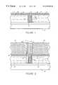
- FIG. 1is an enlarged cross-sectional view of the present invention (see also FIG. 3) showing a semiconductor circuit device fabricated having a metal barrier layer deposited over a low dielectric constant (low K) material layer and a substantially thin ( ⁇ 0.25 ⁇ m) blanket of copper deposited over the metal barrier layer for forming an interconnect structure in accordance with the present invention.
- low Klow dielectric constant
- FIG. 2is an enlarged cross-sectional view of the present invention showing the semiconductor device of FIG. 1 further processed with a photoresist material having an overlying trench region selectively filled with a substantially thick (>>0.25 ⁇ m) amount of copper for forming an interconnect structure in accordance with the present invention.
- FIG. 3is an enlarged cross-sectional view of the present invention showing the semiconductor device of FIG. 2 further processed with the photoresist material and selected portions of the substantially thin layer of copper removed for delineating an elevated structure consisting of the substantially thicker (>>0.25 ⁇ m) amount of copper used to fill the trench region depicted in FIG. 2, in accordance with the present invention.
- FIG. 4is an enlarged cross-sectional view of the present invention showing the semiconductor device of FIG. 3 further processed by removing portions of the metal barrier layer, as depicted in FIG. 1, and deposition of a selective encapsulating metal barrier over the delineated elevated copper structure shown in FIG. 3, in accordance with the present invention.
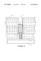
- FIG. 5is an enlarged cross-sectional view of the present invention showing the semiconductor device of FIG. 4 further processed by spin coat formation of a low K dielectric layer formed about the encapsulated copper interconnect structure shown in FIG. 4, and overlying the first low K dielectric material layer, as depicted in FIG. 1, and having a via structure formed for forming additional interconnect structure.
- FIG. 1shows a semiconductor device 10 fabricated to a stage for having a composite copper interconnect structure ( 40 , 53 ) fabricated by a process in accordance with the teaching of the present invention. More particularly, the semiconductor device has been previously fabricated to a stage having integrated circuit elements in need of being electrically energized, and or, being electrically coupled to other integrated circuit elements to perform an electronic function of the semiconductor device 10 .
- the process of the present inventioncomprises forming a first insulating layer 20 over semiconductor substrate 10 .
- First insulating layer 20being formed and selected from a material group characterized as having a lower dielectric constant (low K 1 ) than a dielectric constant of silicon dioxide (SiO 2 ) and silicon nitride (Si 3 N 4 ).
- the preferred material groupconsisting material such as poly(arylene ether) (“PAE”), fluorinated aromatic ether (“FLARE”), fluorinated polymide (“FPI”), benzocyclobutene (“BCB”), hydrogen silsesquioxane (“HSQ”), methyl silsesquioxane (“MSQ”), and xerogel and fluorinated glass.
- the first insulating layer 20has a first access means 21 formed to facilitate formation of an electrical interconnect path and accessing the underlying semiconductor device 10 , said first access means having a walled structure which in a may be in the form of a via structure or a trench structure. As illustrated in FIG. 1, the access means 21 is preferably a via structure 21 .
- first metallic barrier 30formed over first insulating layer 20 .
- the first metallic barrier 30comprises metal material such as tantalum (Ta), tantalum nitride (TaN) and tungsten nitride WN.
- First metallic barrier 30being formed not only to blanket the upper surface 22 of first insulating layer 20 , but also such that the metallic barrier material extends into and lines the walls of the via structure 21 with a metallic barrier measuring less than 25 nm in thickness.
- Via structure 21by example has a diameters measuring less than 0.25 ⁇ m, and a depth dl that is substantially greater than 0.25 ⁇ m.
- FIG. 1further shows a first metal structure 40 , 41 formed from a conductive metal material, which according to the present invention, comprises electroplating copper over planar regions of the metallic barrier 30 and within metallic barrier-lined via region 21 . It should be emphasized that the filled via structure is also substantially thin ( ⁇ 0.25 ⁇ m).
- the conductive metals contemplated by the present inventioncomprise metal, such as copper, which have undesirable diffusion characteristic and which need to be encapsulated to maintain the desirable conductive properties.
- FIG. 2shows a photoresist layer 50 having a thickness d 2 (>>0.25 ⁇ m) that is substantially larger than d 1 .
- Photoresist layer 50facilitates formation, by example, of a trench structure 51 , formed over the previously metal filled via structure 40 , or in accordance with the present invention, over the copper filled via structure 40 .
- FIG. 2further shows formation of a second metal structure 52 within trench structure 51 .
- Metal structure 52in accordance with the present invention, comprises selectively electroplating copper within trench structure 51 . It should be appreciated that trench structure 51 comprises a second access means which could be formed as a via structure.
- the trench structure 51is selectively Cu-electroplated such that the copper is substantially thicker (>>0.25 ⁇ m) than the previously Cu-filled via structure and bonds at metal interface region 54 , (see FIG. 4) with the previously Cu-filled underlying via structure 40 .
- FIG. 3shows an enlarged cross-sectional view of the present invention showing the semiconductor device 10 of FIG. 2 further processed with the photoresist material 50 and selected portions of the second metal structure 52 removed.
- an electropolishing stepremoves the substantially thin blanket of the first metal structure, or copper blanket portion 41 formed on metal barrier 30 to shape the bonded Cu-electroplated via-trench structure 53 , 40 .
- the electropolishing stepis further controlled to stop at the metal barrier 30 on the surface 22 of the low K 1 material 20 to assure that a metallic interface exists for the subsequent metallic capping, or encapsulating step.
- second metal structure 52 and portions of first metal structure 40delineates an elevated metal structure portion 53 .
- Delineated elevated metal structure portion 53being supported by exposed portions 61 of first metallic barrier 30 .
- Elevated metal structure portion 53 and first metal structure portions 40 formed within via structure 21form a composite metal interconnect structure 40 , 53
- the metallic barrier 30is selectively removed by controlling an electropolishing step down to the surface 22 of the low K 1 material 20 .
- exposed metallic regions 61 of metallic barrier 30flare about the metal-filled via structure 40 and are not removed.
- the metallic encapsulating stepcomprises forming a a second metallic barrier 60 over said composite metal interconnect structure 40 , 53 .
- the second metallic barrierbeing selective electroless metal barrier, preferably formed by deposition of CoWP (cobalt-tungsten-phosphide), over the composite metal interconnect structure 40 , 53 .
- Second metallic barrier 60is formed to bond to the exposed metallic regions 61 flaring from the via structure 21 in the low K 1 material 20 .
- the composite metal interconnect structure 40 , 53in accordance with the present invention, comprise bonded Cu electroplated via-trench structure at region 54 and may be termed a copper interconnect structure.
- the first metallic barrier portion 30 and second metallic barrier 60forms an encasement that effectively encapsulates the copper interconnect structure 40 , 53 .
- the encapsulated copper interconnect structure 40 , 53can be further processed to spin coat a low dielectric constant material layer 70 (termed herein as low K 2 material), using the same dielectric material that was used for the low K 1 layer.
- the low K 2 layermay the be further lithographically processed to form a via structure 71 to provide further electrical interconnect means.
- the process of the present inventionfacilitates the use of low dielectric material which results in a semiconductor structure that is free of Si 3 N 4 or SiO 2 , in the copper interconnect region and which comprises copper interconnect structure that overcomes undesirable copper diffusion characteristic.
Landscapes
- Engineering & Computer Science (AREA)
- Physics & Mathematics (AREA)
- Condensed Matter Physics & Semiconductors (AREA)
- General Physics & Mathematics (AREA)
- Computer Hardware Design (AREA)
- Microelectronics & Electronic Packaging (AREA)
- Power Engineering (AREA)
- Manufacturing & Machinery (AREA)
- Internal Circuitry In Semiconductor Integrated Circuit Devices (AREA)
Abstract
Description
Claims (6)
Priority Applications (2)
| Application Number | Priority Date | Filing Date | Title |
|---|---|---|---|
| US09/296,054US6259160B1 (en) | 1999-04-21 | 1999-04-21 | Apparatus and method of encapsulated copper (Cu) Interconnect formation |
| US09/836,054US6455415B1 (en) | 1999-04-21 | 2001-04-16 | Method of encapsulated copper (Cu) interconnect formation |
Applications Claiming Priority (1)
| Application Number | Priority Date | Filing Date | Title |
|---|---|---|---|
| US09/296,054US6259160B1 (en) | 1999-04-21 | 1999-04-21 | Apparatus and method of encapsulated copper (Cu) Interconnect formation |
Related Child Applications (1)
| Application Number | Title | Priority Date | Filing Date |
|---|---|---|---|
| US09/836,054DivisionUS6455415B1 (en) | 1999-04-21 | 2001-04-16 | Method of encapsulated copper (Cu) interconnect formation |
Publications (1)
| Publication Number | Publication Date |
|---|---|
| US6259160B1true US6259160B1 (en) | 2001-07-10 |
Family
ID=23140408
Family Applications (2)
| Application Number | Title | Priority Date | Filing Date |
|---|---|---|---|
| US09/296,054Expired - LifetimeUS6259160B1 (en) | 1999-04-21 | 1999-04-21 | Apparatus and method of encapsulated copper (Cu) Interconnect formation |
| US09/836,054Expired - Fee RelatedUS6455415B1 (en) | 1999-04-21 | 2001-04-16 | Method of encapsulated copper (Cu) interconnect formation |
Family Applications After (1)
| Application Number | Title | Priority Date | Filing Date |
|---|---|---|---|
| US09/836,054Expired - Fee RelatedUS6455415B1 (en) | 1999-04-21 | 2001-04-16 | Method of encapsulated copper (Cu) interconnect formation |
Country Status (1)
| Country | Link |
|---|---|
| US (2) | US6259160B1 (en) |
Cited By (76)
| Publication number | Priority date | Publication date | Assignee | Title |
|---|---|---|---|---|
| US6465340B1 (en)* | 2001-02-06 | 2002-10-15 | Advanced Micro Devices, Inc. | Via filled dual damascene structure with middle stop layer and method for making the same |
| US20020192966A1 (en)* | 2001-06-19 | 2002-12-19 | Shanmugasundram Arulkumar P. | In situ sensor based control of semiconductor processing procedure |
| US20020193902A1 (en)* | 2001-06-19 | 2002-12-19 | Applied Materials, Inc. | Integrating tool, module, and fab level control |
| WO2002103790A1 (en)* | 2001-06-18 | 2002-12-27 | Infineon Technologies North America Corp. | Reduction of via-resistance-shift by increasing via size at a last conductor level of a semiconductor device |
| US20030029383A1 (en)* | 2001-08-13 | 2003-02-13 | Ward Nicholas A. | Dynamic control of wafer processing paths in semiconductor manufacturing processes |
| US20030037090A1 (en)* | 2001-08-14 | 2003-02-20 | Koh Horne L. | Tool services layer for providing tool service functions in conjunction with tool functions |
| US20030036815A1 (en)* | 2001-08-14 | 2003-02-20 | Krishnamurthy Badri N. | Experiment management system, method and medium |
| US6528409B1 (en) | 2002-04-29 | 2003-03-04 | Advanced Micro Devices, Inc. | Interconnect structure formed in porous dielectric material with minimized degradation and electromigration |
| US6528180B1 (en)* | 2000-05-23 | 2003-03-04 | Applied Materials, Inc. | Liner materials |
| US6531779B1 (en)* | 1999-06-29 | 2003-03-11 | Nec Corporation | Multi-layer interconnection structure in semiconductor device and method for fabricating same |
| US20040087148A1 (en)* | 2002-10-30 | 2004-05-06 | Xerox Corporation | Copper interconnect by immersion/electroless plating in dual damascene process |
| US6774486B2 (en) | 2001-10-10 | 2004-08-10 | Micron Technology, Inc. | Circuit boards containing vias and methods for producing same |
| US6869878B1 (en)* | 2003-02-14 | 2005-03-22 | Advanced Micro Devices, Inc. | Method of forming a selective barrier layer using a sacrificial layer |
| US6910947B2 (en) | 2001-06-19 | 2005-06-28 | Applied Materials, Inc. | Control of chemical mechanical polishing pad conditioner directional velocity to improve pad life |
| US6913938B2 (en) | 2001-06-19 | 2005-07-05 | Applied Materials, Inc. | Feedback control of plasma-enhanced chemical vapor deposition processes |
| US20050160575A1 (en)* | 2004-01-22 | 2005-07-28 | International Business Machines Corporation | Integration of high performance copper inductors with bond pads |
| US6927113B1 (en) | 2003-05-23 | 2005-08-09 | Advanced Micro Devices | Semiconductor component and method of manufacture |
| US20050230262A1 (en)* | 2004-04-20 | 2005-10-20 | Semitool, Inc. | Electrochemical methods for the formation of protective features on metallized features |
| US6961626B1 (en) | 2004-05-28 | 2005-11-01 | Applied Materials, Inc | Dynamic offset and feedback threshold |
| US20050275100A1 (en)* | 2004-06-14 | 2005-12-15 | Enthone Inc. | Capping of metal interconnects in integrated circuit electronic devices |
| US20060009129A1 (en)* | 2001-06-19 | 2006-01-12 | Applied Materials, Inc. | Feedforward and feedback control for conditioning of chemical mechanical polishing pad |
| US6999836B2 (en) | 2002-08-01 | 2006-02-14 | Applied Materials, Inc. | Method, system, and medium for handling misrepresentative metrology data within an advanced process control system |
| US20060063370A1 (en)* | 2004-09-21 | 2006-03-23 | Applied Materials, Inc. | Semiconductor device interconnect fabricating techniques |
| US7069101B1 (en) | 1999-07-29 | 2006-06-27 | Applied Materials, Inc. | Computer integrated manufacturing techniques |
| US7082345B2 (en) | 2001-06-19 | 2006-07-25 | Applied Materials, Inc. | Method, system and medium for process control for the matching of tools, chambers and/or other semiconductor-related entities |
| US7096085B2 (en) | 2004-05-28 | 2006-08-22 | Applied Materials | Process control by distinguishing a white noise component of a process variance |
| US7160739B2 (en) | 2001-06-19 | 2007-01-09 | Applied Materials, Inc. | Feedback control of a chemical mechanical polishing device providing manipulation of removal rate profiles |
| US7188142B2 (en) | 2000-11-30 | 2007-03-06 | Applied Materials, Inc. | Dynamic subject information generation in message services of distributed object systems in a semiconductor assembly line facility |
| US7201936B2 (en) | 2001-06-19 | 2007-04-10 | Applied Materials, Inc. | Method of feedback control of sub-atmospheric chemical vapor deposition processes |
| US7205228B2 (en) | 2003-06-03 | 2007-04-17 | Applied Materials, Inc. | Selective metal encapsulation schemes |
| US7215000B2 (en) | 2004-08-23 | 2007-05-08 | Texas Instruments Incorporated | Selectively encased surface metal structures in a semiconductor device |
| US7225047B2 (en) | 2002-03-19 | 2007-05-29 | Applied Materials, Inc. | Method, system and medium for controlling semiconductor wafer processes using critical dimension measurements |
| US20070178690A1 (en)* | 2006-01-31 | 2007-08-02 | Markus Nopper | Semiconductor device comprising a metallization layer stack with a porous low-k material having an enhanced integrity |
| US7272459B2 (en) | 2002-11-15 | 2007-09-18 | Applied Materials, Inc. | Method, system and medium for controlling manufacture process having multivariate input parameters |
| US20070269978A1 (en)* | 2006-05-18 | 2007-11-22 | Chien-Hsueh Shih | Process for improving copper line cap formation |
| US7333871B2 (en) | 2003-01-21 | 2008-02-19 | Applied Materials, Inc. | Automated design and execution of experiments with integrated model creation for semiconductor manufacturing tools |
| US7337019B2 (en) | 2001-07-16 | 2008-02-26 | Applied Materials, Inc. | Integration of fault detection with run-to-run control |
| US7354332B2 (en) | 2003-08-04 | 2008-04-08 | Applied Materials, Inc. | Technique for process-qualifying a semiconductor manufacturing tool using metrology data |
| US7356377B2 (en) | 2004-01-29 | 2008-04-08 | Applied Materials, Inc. | System, method, and medium for monitoring performance of an advanced process control system |
| US20080277759A1 (en)* | 2005-07-27 | 2008-11-13 | Anil Kumar Chinthakindi | Post last wiring level inductor using patterned plate process |
| US20090079084A1 (en)* | 2007-09-24 | 2009-03-26 | Research Triangle Institute | Preventing breakage of long metal signal conductors on semiconductor substrates |
| US20090294901A1 (en)* | 2008-06-03 | 2009-12-03 | International Business Machines Corporation | Structure and method of forming electrically blown metal fuses for integrated circuits |
| US7698012B2 (en) | 2001-06-19 | 2010-04-13 | Applied Materials, Inc. | Dynamic metrology schemes and sampling schemes for advanced process control in semiconductor processing |
| US20100187665A1 (en)* | 2009-01-26 | 2010-07-29 | Sixis, Inc. | Integral metal structure with conductive post portions |
| US20100200540A1 (en)* | 2007-09-25 | 2010-08-12 | Sixis, Inc. | Large substrate structural vias |
| US20100221911A1 (en)* | 2009-02-27 | 2010-09-02 | Oliver Aubel | Providing superior electromigration performance and reducing deterioration of sensitive low-k dielectrics in metallization systems of semiconductor devices |
| US20100295181A1 (en)* | 2009-05-19 | 2010-11-25 | International Business Machines Corporation | Redundant metal barrier structure for interconnect applications |
| US20110193199A1 (en)* | 2010-02-09 | 2011-08-11 | International Business Machines Corporation | Electromigration immune through-substrate vias |
| US20120261719A1 (en)* | 2009-08-11 | 2012-10-18 | International Business Machines Corporation | Heterojunction bipolar transistors and methods of manufacture |
| US8835305B2 (en) | 2012-07-31 | 2014-09-16 | International Business Machines Corporation | Method of fabricating a profile control in interconnect structures |
| US20150137376A1 (en)* | 2012-11-12 | 2015-05-21 | Taiwan Semiconductor Manufacturing Company, Ltd. | Semiconductor Structure and Semiconductor Fabricating Process for the Same |
| US9859152B2 (en)* | 2012-12-14 | 2018-01-02 | Taiwan Semiconductor Manufacturing Company, Ltd. | Protecting layer in a semiconductor structure |
| US9859219B1 (en) | 2017-01-24 | 2018-01-02 | International Business Machines Corporation | Copper wiring structures with copper titanium encapsulation |
| KR20180034671A (en)* | 2015-08-25 | 2018-04-04 | 인벤사스 본딩 테크놀로지스 인코포레이티드 | Conductive Barrier Direct Hybrid Junction |
| US10734277B2 (en)* | 2018-11-19 | 2020-08-04 | International Business Machines Corporation | Top via back end of the line interconnect integration |
| US10840205B2 (en) | 2017-09-24 | 2020-11-17 | Invensas Bonding Technologies, Inc. | Chemical mechanical polishing for hybrid bonding |
| US11011494B2 (en) | 2018-08-31 | 2021-05-18 | Invensas Bonding Technologies, Inc. | Layer structures for making direct metal-to-metal bonds at low temperatures in microelectronics |
| US11011418B2 (en) | 2005-08-11 | 2021-05-18 | Invensas Bonding Technologies, Inc. | 3D IC method and device |
| US11133218B1 (en)* | 2020-01-23 | 2021-09-28 | Tae Young Lee | Semiconductor apparatus having through silicon via structure and manufacturing method thereof |
| CN113517257A (en)* | 2020-04-09 | 2021-10-19 | 中国科学院微电子研究所 | Semiconductor structure and method of making the same |
| US11158573B2 (en) | 2018-10-22 | 2021-10-26 | Invensas Bonding Technologies, Inc. | Interconnect structures |
| US20210375816A1 (en)* | 2020-06-02 | 2021-12-02 | Texas Instruments Incorporated | Ic device with chip to package interconnects from a copper metal interconnect level |
| US11244920B2 (en) | 2018-12-18 | 2022-02-08 | Invensas Bonding Technologies, Inc. | Method and structures for low temperature device bonding |
| US11393779B2 (en) | 2018-06-13 | 2022-07-19 | Invensas Bonding Technologies, Inc. | Large metal pads over TSV |
| US11515279B2 (en) | 2018-04-11 | 2022-11-29 | Adeia Semiconductor Bonding Technologies Inc. | Low temperature bonded structures |
| US11710718B2 (en) | 2015-07-10 | 2023-07-25 | Adeia Semiconductor Technologies Llc | Structures and methods for low temperature bonding using nanoparticles |
| US11728313B2 (en) | 2018-06-13 | 2023-08-15 | Adeia Semiconductor Bonding Technologies Inc. | Offset pads over TSV |
| US11735523B2 (en) | 2020-05-19 | 2023-08-22 | Adeia Semiconductor Bonding Technologies Inc. | Laterally unconfined structure |
| US11804377B2 (en) | 2018-04-05 | 2023-10-31 | Adeia Semiconductor Bonding Technologies, Inc. | Method for preparing a surface for direct-bonding |
| US11894326B2 (en) | 2017-03-17 | 2024-02-06 | Adeia Semiconductor Bonding Technologies Inc. | Multi-metal contact structure |
| US11908739B2 (en) | 2017-06-05 | 2024-02-20 | Adeia Semiconductor Technologies Llc | Flat metal features for microelectronics applications |
| US11929347B2 (en) | 2020-10-20 | 2024-03-12 | Adeia Semiconductor Technologies Llc | Mixed exposure for large die |
| US11973056B2 (en) | 2016-10-27 | 2024-04-30 | Adeia Semiconductor Technologies Llc | Methods for low temperature bonding using nanoparticles |
| US12100676B2 (en) | 2018-04-11 | 2024-09-24 | Adeia Semiconductor Bonding Technologies Inc. | Low temperature bonded structures |
| US12211809B2 (en) | 2020-12-30 | 2025-01-28 | Adeia Semiconductor Bonding Technologies Inc. | Structure with conductive feature and method of forming same |
| US12381128B2 (en) | 2020-12-28 | 2025-08-05 | Adeia Semiconductor Bonding Technologies Inc. | Structures with through-substrate vias and methods for forming the same |
Families Citing this family (10)
| Publication number | Priority date | Publication date | Assignee | Title |
|---|---|---|---|---|
| US7119008B2 (en)* | 2000-09-18 | 2006-10-10 | Acm Research, Inc. | Integrating metal layers with ultra low-K dielectrics |
| US6875322B1 (en) | 2003-01-15 | 2005-04-05 | Lam Research Corporation | Electrochemical assisted CMP |
| US6753248B1 (en) | 2003-01-27 | 2004-06-22 | Applied Materials, Inc. | Post metal barrier/adhesion film |
| JP3910973B2 (en)* | 2004-04-22 | 2007-04-25 | 株式会社東芝 | Manufacturing method of semiconductor device |
| US20060138668A1 (en)* | 2004-12-27 | 2006-06-29 | Hung-Wen Su | Passivation structure for semiconductor devices |
| US20060216929A1 (en)* | 2005-03-28 | 2006-09-28 | Hyun-Mog Park | Etch stopless dual damascene structure and method of fabrication |
| US8723321B2 (en)* | 2006-06-08 | 2014-05-13 | GLOBALFOUNDIES Inc. | Copper interconnects with improved electromigration lifetime |
| KR20100077535A (en)* | 2008-12-29 | 2010-07-08 | 주식회사 하이닉스반도체 | Contact structure, method of manufacturing the same, phase changeable memory device having the same and method of manufacturing the phase changeable memory device |
| US9099465B2 (en)* | 2013-10-14 | 2015-08-04 | Stmicroelectronics, Inc. | High aspect ratio vias for high performance devices |
| US11817389B2 (en) | 2020-03-24 | 2023-11-14 | International Business Machines Corporation | Multi-metal interconnects for semiconductor device structures |
Citations (2)
| Publication number | Priority date | Publication date | Assignee | Title |
|---|---|---|---|---|
| US5695810A (en) | 1996-11-20 | 1997-12-09 | Cornell Research Foundation, Inc. | Use of cobalt tungsten phosphide as a barrier material for copper metallization |
| US5856707A (en)* | 1995-09-11 | 1999-01-05 | Stmicroelectronics, Inc. | Vias and contact plugs with an aspect ratio lower than the aspect ratio of the structure in which they are formed |
Family Cites Families (4)
| Publication number | Priority date | Publication date | Assignee | Title |
|---|---|---|---|---|
| US5612254A (en)* | 1992-06-29 | 1997-03-18 | Intel Corporation | Methods of forming an interconnect on a semiconductor substrate |
| US5567300A (en)* | 1994-09-02 | 1996-10-22 | Ibm Corporation | Electrochemical metal removal technique for planarization of surfaces |
| US6100184A (en)* | 1997-08-20 | 2000-08-08 | Sematech, Inc. | Method of making a dual damascene interconnect structure using low dielectric constant material for an inter-level dielectric layer |
| US6146986A (en)* | 1999-01-08 | 2000-11-14 | Lam Research Corporation | Lithographic method for creating damascene metallization layers |
- 1999
- 1999-04-21USUS09/296,054patent/US6259160B1/ennot_activeExpired - Lifetime
- 2001
- 2001-04-16USUS09/836,054patent/US6455415B1/ennot_activeExpired - Fee Related
Patent Citations (2)
| Publication number | Priority date | Publication date | Assignee | Title |
|---|---|---|---|---|
| US5856707A (en)* | 1995-09-11 | 1999-01-05 | Stmicroelectronics, Inc. | Vias and contact plugs with an aspect ratio lower than the aspect ratio of the structure in which they are formed |
| US5695810A (en) | 1996-11-20 | 1997-12-09 | Cornell Research Foundation, Inc. | Use of cobalt tungsten phosphide as a barrier material for copper metallization |
Non-Patent Citations (6)
| Title |
|---|
| "Electroless CoWP Barrier/Protection Layer Deposition for Cu Metallization", S. Lopatin, et al., Material Research Society, Symp. Proc. vol. 451, 1997, pp. 463-468. |
| "High Aspect Ratio Quarter-micron Electroless Copper Integrated Technology", Yosi Shacham-Diamond, et al., Microelectric Engineering 37/38, 1997, pp. 77-88. |
| "Processing and Integration of Copper Interconnects," Robert L. Jackson, et al.,Solid State Technology, Mar. 1998, Penn Well Publishing Company (15 pages). |
| "Smokin . . . Watch Out, Fast Computers Are on the Way Speed Is Now Pushing Computer Power," Andy Maslowski, Apr./May/Jun. 1998, vol. 25, No. 2, pp. 1 and 20 The Electron, published at 4781 E. 355th Street, Willoughby, Ohio, 44094-4698. |
| "Tantalum, Copper and Damascene: The future of Interconnects," Peter Singer, Semiconductor International, Jun. 1998, (7 pages). |
| IBM Technical Disclosure Bulletin, No. 9, Feb. 1992.* |
Cited By (156)
| Publication number | Priority date | Publication date | Assignee | Title |
|---|---|---|---|---|
| US6777324B2 (en) | 1999-06-29 | 2004-08-17 | Nec Electronics Corporation | Multi-layer interconnection structure in semiconductor device and method for fabricating same |
| US6531779B1 (en)* | 1999-06-29 | 2003-03-11 | Nec Corporation | Multi-layer interconnection structure in semiconductor device and method for fabricating same |
| US7069101B1 (en) | 1999-07-29 | 2006-06-27 | Applied Materials, Inc. | Computer integrated manufacturing techniques |
| US7174230B2 (en) | 1999-07-29 | 2007-02-06 | Applied Materials, Inc. | Computer integrated manufacturing techniques |
| US6528180B1 (en)* | 2000-05-23 | 2003-03-04 | Applied Materials, Inc. | Liner materials |
| US8504620B2 (en) | 2000-11-30 | 2013-08-06 | Applied Materials, Inc. | Dynamic subject information generation in message services of distributed object systems |
| US7188142B2 (en) | 2000-11-30 | 2007-03-06 | Applied Materials, Inc. | Dynamic subject information generation in message services of distributed object systems in a semiconductor assembly line facility |
| US6465340B1 (en)* | 2001-02-06 | 2002-10-15 | Advanced Micro Devices, Inc. | Via filled dual damascene structure with middle stop layer and method for making the same |
| WO2002103790A1 (en)* | 2001-06-18 | 2002-12-27 | Infineon Technologies North America Corp. | Reduction of via-resistance-shift by increasing via size at a last conductor level of a semiconductor device |
| US6913938B2 (en) | 2001-06-19 | 2005-07-05 | Applied Materials, Inc. | Feedback control of plasma-enhanced chemical vapor deposition processes |
| US20050208879A1 (en)* | 2001-06-19 | 2005-09-22 | Applied Materials | Control of chemical mechanical polishing pad conditioner directional velocity to improve pad life |
| US7040956B2 (en) | 2001-06-19 | 2006-05-09 | Applied Materials, Inc. | Control of chemical mechanical polishing pad conditioner directional velocity to improve pad life |
| US7725208B2 (en) | 2001-06-19 | 2010-05-25 | Applied Materials, Inc. | Dynamic metrology schemes and sampling schemes for advanced process control in semiconductor processing |
| US7160739B2 (en) | 2001-06-19 | 2007-01-09 | Applied Materials, Inc. | Feedback control of a chemical mechanical polishing device providing manipulation of removal rate profiles |
| US7101799B2 (en) | 2001-06-19 | 2006-09-05 | Applied Materials, Inc. | Feedforward and feedback control for conditioning of chemical mechanical polishing pad |
| US6910947B2 (en) | 2001-06-19 | 2005-06-28 | Applied Materials, Inc. | Control of chemical mechanical polishing pad conditioner directional velocity to improve pad life |
| US7201936B2 (en) | 2001-06-19 | 2007-04-10 | Applied Materials, Inc. | Method of feedback control of sub-atmospheric chemical vapor deposition processes |
| US8694145B2 (en) | 2001-06-19 | 2014-04-08 | Applied Materials, Inc. | Feedback control of a chemical mechanical polishing device providing manipulation of removal rate profiles |
| US7698012B2 (en) | 2001-06-19 | 2010-04-13 | Applied Materials, Inc. | Dynamic metrology schemes and sampling schemes for advanced process control in semiconductor processing |
| US7082345B2 (en) | 2001-06-19 | 2006-07-25 | Applied Materials, Inc. | Method, system and medium for process control for the matching of tools, chambers and/or other semiconductor-related entities |
| US20020193902A1 (en)* | 2001-06-19 | 2002-12-19 | Applied Materials, Inc. | Integrating tool, module, and fab level control |
| US8070909B2 (en) | 2001-06-19 | 2011-12-06 | Applied Materials, Inc. | Feedback control of chemical mechanical polishing device providing manipulation of removal rate profiles |
| US7783375B2 (en) | 2001-06-19 | 2010-08-24 | Applied Materials, Inc. | Dynamic metrology schemes and sampling schemes for advanced process control in semiconductor processing |
| US20020192966A1 (en)* | 2001-06-19 | 2002-12-19 | Shanmugasundram Arulkumar P. | In situ sensor based control of semiconductor processing procedure |
| US7047099B2 (en) | 2001-06-19 | 2006-05-16 | Applied Materials Inc. | Integrating tool, module, and fab level control |
| US20060009129A1 (en)* | 2001-06-19 | 2006-01-12 | Applied Materials, Inc. | Feedforward and feedback control for conditioning of chemical mechanical polishing pad |
| US7337019B2 (en) | 2001-07-16 | 2008-02-26 | Applied Materials, Inc. | Integration of fault detection with run-to-run control |
| US6950716B2 (en) | 2001-08-13 | 2005-09-27 | Applied Materials, Inc. | Dynamic control of wafer processing paths in semiconductor manufacturing processes |
| US20030029383A1 (en)* | 2001-08-13 | 2003-02-13 | Ward Nicholas A. | Dynamic control of wafer processing paths in semiconductor manufacturing processes |
| US6984198B2 (en) | 2001-08-14 | 2006-01-10 | Applied Materials, Inc. | Experiment management system, method and medium |
| US20030037090A1 (en)* | 2001-08-14 | 2003-02-20 | Koh Horne L. | Tool services layer for providing tool service functions in conjunction with tool functions |
| US20030036815A1 (en)* | 2001-08-14 | 2003-02-20 | Krishnamurthy Badri N. | Experiment management system, method and medium |
| US6774486B2 (en) | 2001-10-10 | 2004-08-10 | Micron Technology, Inc. | Circuit boards containing vias and methods for producing same |
| US6797616B2 (en) | 2001-10-10 | 2004-09-28 | Micron Technology, Inc. | Circuit boards containing vias and methods for producing same |
| US7225047B2 (en) | 2002-03-19 | 2007-05-29 | Applied Materials, Inc. | Method, system and medium for controlling semiconductor wafer processes using critical dimension measurements |
| US6528409B1 (en) | 2002-04-29 | 2003-03-04 | Advanced Micro Devices, Inc. | Interconnect structure formed in porous dielectric material with minimized degradation and electromigration |
| US6999836B2 (en) | 2002-08-01 | 2006-02-14 | Applied Materials, Inc. | Method, system, and medium for handling misrepresentative metrology data within an advanced process control system |
| US20040087148A1 (en)* | 2002-10-30 | 2004-05-06 | Xerox Corporation | Copper interconnect by immersion/electroless plating in dual damascene process |
| US7966087B2 (en) | 2002-11-15 | 2011-06-21 | Applied Materials, Inc. | Method, system and medium for controlling manufacture process having multivariate input parameters |
| US7272459B2 (en) | 2002-11-15 | 2007-09-18 | Applied Materials, Inc. | Method, system and medium for controlling manufacture process having multivariate input parameters |
| US7333871B2 (en) | 2003-01-21 | 2008-02-19 | Applied Materials, Inc. | Automated design and execution of experiments with integrated model creation for semiconductor manufacturing tools |
| US6869878B1 (en)* | 2003-02-14 | 2005-03-22 | Advanced Micro Devices, Inc. | Method of forming a selective barrier layer using a sacrificial layer |
| US6927113B1 (en) | 2003-05-23 | 2005-08-09 | Advanced Micro Devices | Semiconductor component and method of manufacture |
| US7205228B2 (en) | 2003-06-03 | 2007-04-17 | Applied Materials, Inc. | Selective metal encapsulation schemes |
| US7354332B2 (en) | 2003-08-04 | 2008-04-08 | Applied Materials, Inc. | Technique for process-qualifying a semiconductor manufacturing tool using metrology data |
| US20050160575A1 (en)* | 2004-01-22 | 2005-07-28 | International Business Machines Corporation | Integration of high performance copper inductors with bond pads |
| US7207096B2 (en) | 2004-01-22 | 2007-04-24 | International Business Machines Corporation | Method of manufacturing high performance copper inductors with bond pads |
| US7356377B2 (en) | 2004-01-29 | 2008-04-08 | Applied Materials, Inc. | System, method, and medium for monitoring performance of an advanced process control system |
| US20050230262A1 (en)* | 2004-04-20 | 2005-10-20 | Semitool, Inc. | Electrochemical methods for the formation of protective features on metallized features |
| US7221990B2 (en) | 2004-05-28 | 2007-05-22 | Applied Materials, Inc. | Process control by distinguishing a white noise component of a process variance |
| US7349753B2 (en) | 2004-05-28 | 2008-03-25 | Applied Materials, Inc. | Adjusting manufacturing process control parameter using updated process threshold derived from uncontrollable error |
| US6961626B1 (en) | 2004-05-28 | 2005-11-01 | Applied Materials, Inc | Dynamic offset and feedback threshold |
| US7096085B2 (en) | 2004-05-28 | 2006-08-22 | Applied Materials | Process control by distinguishing a white noise component of a process variance |
| US20070298609A1 (en)* | 2004-06-14 | 2007-12-27 | Enthone Inc. | Capping of metal interconnects in integrated circuit electronic devices |
| US7268074B2 (en) | 2004-06-14 | 2007-09-11 | Enthone, Inc. | Capping of metal interconnects in integrated circuit electronic devices |
| US7393781B2 (en) | 2004-06-14 | 2008-07-01 | Enthone Inc. | Capping of metal interconnects in integrated circuit electronic devices |
| US20050275100A1 (en)* | 2004-06-14 | 2005-12-15 | Enthone Inc. | Capping of metal interconnects in integrated circuit electronic devices |
| US7215000B2 (en) | 2004-08-23 | 2007-05-08 | Texas Instruments Incorporated | Selectively encased surface metal structures in a semiconductor device |
| US7312146B2 (en) | 2004-09-21 | 2007-12-25 | Applied Materials, Inc. | Semiconductor device interconnect fabricating techniques |
| US20060063370A1 (en)* | 2004-09-21 | 2006-03-23 | Applied Materials, Inc. | Semiconductor device interconnect fabricating techniques |
| US20080277759A1 (en)* | 2005-07-27 | 2008-11-13 | Anil Kumar Chinthakindi | Post last wiring level inductor using patterned plate process |
| US20080293233A1 (en)* | 2005-07-27 | 2008-11-27 | Anil Kumar Chinthakindi | Post last wiring level inductor using patterned plate process |
| US7763954B2 (en)* | 2005-07-27 | 2010-07-27 | International Business Machines Corporation | Post last wiring level inductor using patterned plate process |
| US20080290458A1 (en)* | 2005-07-27 | 2008-11-27 | Anil Kumar Chinthakindi | Post last wiring level inductor using patterned plate process |
| US20080293210A1 (en)* | 2005-07-27 | 2008-11-27 | Anil Kumar Chinthakindi | Post last wiring level inductor using patterned plate process |
| US7741698B2 (en) | 2005-07-27 | 2010-06-22 | International Business Machines Corporation | Post last wiring level inductor using patterned plate process |
| US7732294B2 (en) | 2005-07-27 | 2010-06-08 | International Business Machines Corporation | Post last wiring level inductor using patterned plate process |
| US7732295B2 (en) | 2005-07-27 | 2010-06-08 | International Business Machines Corporation | Post last wiring level inductor using patterned plate process |
| US11515202B2 (en) | 2005-08-11 | 2022-11-29 | Adeia Semiconductor Bonding Technologies Inc. | 3D IC method and device |
| US11011418B2 (en) | 2005-08-11 | 2021-05-18 | Invensas Bonding Technologies, Inc. | 3D IC method and device |
| US11289372B2 (en) | 2005-08-11 | 2022-03-29 | Invensas Bonding Technologies, Inc. | 3D IC method and device |
| DE102006004429A1 (en)* | 2006-01-31 | 2007-08-02 | Advanced Micro Devices, Inc., Sunnyvale | Forming metallization layers for high-density integrated circuit component interconnection, also deposits dielectric material of low permitivity |
| US20070178690A1 (en)* | 2006-01-31 | 2007-08-02 | Markus Nopper | Semiconductor device comprising a metallization layer stack with a porous low-k material having an enhanced integrity |
| US8623760B2 (en) | 2006-05-18 | 2014-01-07 | Taiwan Semiconductor Manufacturing Company, Ltd. | Process for improving copper line cap formation |
| US8193087B2 (en) | 2006-05-18 | 2012-06-05 | Taiwan Semiconductor Manufacturing Co., Ltd. | Process for improving copper line cap formation |
| US20070269978A1 (en)* | 2006-05-18 | 2007-11-22 | Chien-Hsueh Shih | Process for improving copper line cap formation |
| US7944041B2 (en) | 2007-09-24 | 2011-05-17 | Research Triangle Institute | Integrated semiconductor substrate structure using incompatible processes |
| US20090079059A1 (en)* | 2007-09-24 | 2009-03-26 | Research Triangle Institute | Integrated semiconductor substrate structure using incompatible processes |
| US8404585B2 (en) | 2007-09-24 | 2013-03-26 | Research Triangle Institute | Preventing breakage of long metal signal conductors on semiconductor substrates |
| US7831874B2 (en) | 2007-09-24 | 2010-11-09 | Sixis, Inc. | Local defect memories on semiconductor substrates in a stack computer |
| US20090079058A1 (en)* | 2007-09-24 | 2009-03-26 | Research Triangle Institute | Semiconductor substrate elastomeric stack |
| US20110183469A1 (en)* | 2007-09-24 | 2011-07-28 | Research Triangle Institute | Integrated semiconductor substrate structure using incompatible processes |
| US20090079084A1 (en)* | 2007-09-24 | 2009-03-26 | Research Triangle Institute | Preventing breakage of long metal signal conductors on semiconductor substrates |
| US7999388B2 (en)* | 2007-09-24 | 2011-08-16 | Research Triangle Institute | Preventing breakage of long metal signal conductors on semiconductor substrates |
| US7829994B2 (en) | 2007-09-24 | 2010-11-09 | Sixis, Inc. | Semiconductor substrate elastomeric stack |
| US8222086B2 (en) | 2007-09-24 | 2012-07-17 | Research Triangle Institute | Integrated semiconductor substrate structure using incompatible processes |
| US20100200540A1 (en)* | 2007-09-25 | 2010-08-12 | Sixis, Inc. | Large substrate structural vias |
| US8008134B2 (en) | 2007-09-25 | 2011-08-30 | Research Triangle Institute | Large substrate structural vias |
| US20090294901A1 (en)* | 2008-06-03 | 2009-12-03 | International Business Machines Corporation | Structure and method of forming electrically blown metal fuses for integrated circuits |
| US7737528B2 (en) | 2008-06-03 | 2010-06-15 | International Business Machines Corporation | Structure and method of forming electrically blown metal fuses for integrated circuits |
| US8129834B2 (en) | 2009-01-26 | 2012-03-06 | Research Triangle Institute | Integral metal structure with conductive post portions |
| US20100187665A1 (en)* | 2009-01-26 | 2010-07-29 | Sixis, Inc. | Integral metal structure with conductive post portions |
| DE102009010844A1 (en)* | 2009-02-27 | 2010-09-02 | Advanced Micro Devices, Inc., Sunnyvale | Providing enhanced electromigration performance and reducing the degradation of sensitive low-k dielectric materials in metallization systems of semiconductor devices |
| US20100221911A1 (en)* | 2009-02-27 | 2010-09-02 | Oliver Aubel | Providing superior electromigration performance and reducing deterioration of sensitive low-k dielectrics in metallization systems of semiconductor devices |
| DE102009010844B4 (en)* | 2009-02-27 | 2018-10-11 | Advanced Micro Devices, Inc. | Providing enhanced electromigration performance and reducing the degradation of sensitive low-k dielectric materials in metallization systems of semiconductor devices |
| US8153524B2 (en) | 2009-02-27 | 2012-04-10 | Advanced Micro Devices, Inc. | Providing superior electromigration performance and reducing deterioration of sensitive low-k dielectrics in metallization systems of semiconductor devices |
| US20100295181A1 (en)* | 2009-05-19 | 2010-11-25 | International Business Machines Corporation | Redundant metal barrier structure for interconnect applications |
| US8242600B2 (en) | 2009-05-19 | 2012-08-14 | International Business Machines Corporation | Redundant metal barrier structure for interconnect applications |
| US8592306B2 (en) | 2009-05-19 | 2013-11-26 | International Business Machines Corporation | Redundant metal barrier structure for interconnect applications |
| US8692288B2 (en)* | 2009-08-11 | 2014-04-08 | International Business Machines Corporation | Heterojunction bipolar transistors and methods of manufacture |
| US8633106B2 (en) | 2009-08-11 | 2014-01-21 | International Business Machines Corporation | Heterojunction bipolar transistors and methods of manufacture |
| US20120261719A1 (en)* | 2009-08-11 | 2012-10-18 | International Business Machines Corporation | Heterojunction bipolar transistors and methods of manufacture |
| US9153558B2 (en) | 2010-02-09 | 2015-10-06 | International Business Machines Corporation | Electromigration immune through-substrate vias |
| US20110193199A1 (en)* | 2010-02-09 | 2011-08-11 | International Business Machines Corporation | Electromigration immune through-substrate vias |
| US8304863B2 (en) | 2010-02-09 | 2012-11-06 | International Business Machines Corporation | Electromigration immune through-substrate vias |
| US9105641B2 (en) | 2012-07-31 | 2015-08-11 | International Business Machines Corporation | Profile control in interconnect structures |
| US8835305B2 (en) | 2012-07-31 | 2014-09-16 | International Business Machines Corporation | Method of fabricating a profile control in interconnect structures |
| US20150137376A1 (en)* | 2012-11-12 | 2015-05-21 | Taiwan Semiconductor Manufacturing Company, Ltd. | Semiconductor Structure and Semiconductor Fabricating Process for the Same |
| US9576893B2 (en)* | 2012-11-12 | 2017-02-21 | Taiwan Semiconductor Manufacturing Company, Ltd. | Semiconductor structure and semiconductor fabricating process for the same |
| US9859152B2 (en)* | 2012-12-14 | 2018-01-02 | Taiwan Semiconductor Manufacturing Company, Ltd. | Protecting layer in a semiconductor structure |
| US11710718B2 (en) | 2015-07-10 | 2023-07-25 | Adeia Semiconductor Technologies Llc | Structures and methods for low temperature bonding using nanoparticles |
| US10262963B2 (en) | 2015-08-25 | 2019-04-16 | Invensas Bonding Technologies, Inc. | Conductive barrier direct hybrid bonding |
| US12381168B2 (en) | 2015-08-25 | 2025-08-05 | Adeia Semiconductor Bonding Technologies Inc. | Conductive barrier direct hybrid bonding |
| US9953941B2 (en)* | 2015-08-25 | 2018-04-24 | Invensas Bonding Technologies, Inc. | Conductive barrier direct hybrid bonding |
| KR20180034671A (en)* | 2015-08-25 | 2018-04-04 | 인벤사스 본딩 테크놀로지스 인코포레이티드 | Conductive Barrier Direct Hybrid Junction |
| US11830838B2 (en) | 2015-08-25 | 2023-11-28 | Adeia Semiconductor Bonding Technologies Inc. | Conductive barrier direct hybrid bonding |
| KR20220083859A (en)* | 2015-08-25 | 2022-06-20 | 인벤사스 본딩 테크놀로지스 인코포레이티드 | Conductive barrier direct hybrid bonding |
| US11264345B2 (en) | 2015-08-25 | 2022-03-01 | Invensas Bonding Technologies, Inc. | Conductive barrier direct hybrid bonding |
| US12027487B2 (en) | 2016-10-27 | 2024-07-02 | Adeia Semiconductor Technologies Llc | Structures for low temperature bonding using nanoparticles |
| US11973056B2 (en) | 2016-10-27 | 2024-04-30 | Adeia Semiconductor Technologies Llc | Methods for low temperature bonding using nanoparticles |
| US9859219B1 (en) | 2017-01-24 | 2018-01-02 | International Business Machines Corporation | Copper wiring structures with copper titanium encapsulation |
| US11894326B2 (en) | 2017-03-17 | 2024-02-06 | Adeia Semiconductor Bonding Technologies Inc. | Multi-metal contact structure |
| US11908739B2 (en) | 2017-06-05 | 2024-02-20 | Adeia Semiconductor Technologies Llc | Flat metal features for microelectronics applications |
| US12381173B2 (en) | 2017-09-24 | 2025-08-05 | Adeia Semiconductor Bonding Technologies Inc. | Direct hybrid bonding of substrates having microelectronic components with different profiles and/or pitches at the bonding interface |
| US10840205B2 (en) | 2017-09-24 | 2020-11-17 | Invensas Bonding Technologies, Inc. | Chemical mechanical polishing for hybrid bonding |
| US11552041B2 (en) | 2017-09-24 | 2023-01-10 | Adeia Semiconductor Bonding Technologies Inc. | Chemical mechanical polishing for hybrid bonding |
| US11804377B2 (en) | 2018-04-05 | 2023-10-31 | Adeia Semiconductor Bonding Technologies, Inc. | Method for preparing a surface for direct-bonding |
| US12341018B2 (en) | 2018-04-05 | 2025-06-24 | Adeia Semiconductor Bonding Technologies Inc. | Method for preparing a surface for direct-bonding |
| US12100676B2 (en) | 2018-04-11 | 2024-09-24 | Adeia Semiconductor Bonding Technologies Inc. | Low temperature bonded structures |
| US12132020B2 (en) | 2018-04-11 | 2024-10-29 | Adeia Semiconductor Bonding Technologies Inc. | Low temperature bonded structures |
| US11515279B2 (en) | 2018-04-11 | 2022-11-29 | Adeia Semiconductor Bonding Technologies Inc. | Low temperature bonded structures |
| US12046571B2 (en) | 2018-04-11 | 2024-07-23 | Adeia Semiconductor Bonding Technologies Inc. | Low temperature bonded structures |
| US12243851B2 (en) | 2018-06-13 | 2025-03-04 | Adeia Semiconductor Bonding Technologies Inc. | Offset pads over TSV |
| US11749645B2 (en) | 2018-06-13 | 2023-09-05 | Adeia Semiconductor Bonding Technologies Inc. | TSV as pad |
| US12205926B2 (en) | 2018-06-13 | 2025-01-21 | Adeia Semiconductor Bonding Technologies Inc. | TSV as pad |
| US11728313B2 (en) | 2018-06-13 | 2023-08-15 | Adeia Semiconductor Bonding Technologies Inc. | Offset pads over TSV |
| US11393779B2 (en) | 2018-06-13 | 2022-07-19 | Invensas Bonding Technologies, Inc. | Large metal pads over TSV |
| US11955445B2 (en) | 2018-06-13 | 2024-04-09 | Adeia Semiconductor Bonding Technologies Inc. | Metal pads over TSV |
| US12136605B2 (en) | 2018-08-31 | 2024-11-05 | Adeia Semiconductor Bonding Technologies Inc. | Layer structures for making direct metal-to-metal bonds at low temperatures in microelectronics and method for forming the same |
| US11011494B2 (en) | 2018-08-31 | 2021-05-18 | Invensas Bonding Technologies, Inc. | Layer structures for making direct metal-to-metal bonds at low temperatures in microelectronics |
| US11158573B2 (en) | 2018-10-22 | 2021-10-26 | Invensas Bonding Technologies, Inc. | Interconnect structures |
| US11756880B2 (en) | 2018-10-22 | 2023-09-12 | Adeia Semiconductor Bonding Technologies Inc. | Interconnect structures |
| US12125784B2 (en) | 2018-10-22 | 2024-10-22 | Adeia Semiconductor Bonding Technologies Inc. | Interconnect structures |
| US10734277B2 (en)* | 2018-11-19 | 2020-08-04 | International Business Machines Corporation | Top via back end of the line interconnect integration |
| US11244920B2 (en) | 2018-12-18 | 2022-02-08 | Invensas Bonding Technologies, Inc. | Method and structures for low temperature device bonding |
| US12154880B2 (en) | 2018-12-18 | 2024-11-26 | Adeia Semiconductor Bonding Technologies Inc. | Method and structures for low temperature device bonding |
| US11133218B1 (en)* | 2020-01-23 | 2021-09-28 | Tae Young Lee | Semiconductor apparatus having through silicon via structure and manufacturing method thereof |
| CN113517257A (en)* | 2020-04-09 | 2021-10-19 | 中国科学院微电子研究所 | Semiconductor structure and method of making the same |
| CN113517257B (en)* | 2020-04-09 | 2024-04-16 | 中国科学院微电子研究所 | Semiconductor structure and method for manufacturing the same |
| US11735523B2 (en) | 2020-05-19 | 2023-08-22 | Adeia Semiconductor Bonding Technologies Inc. | Laterally unconfined structure |
| US12033943B2 (en) | 2020-05-19 | 2024-07-09 | Adeia Semiconductor Bonding Technologies Inc. | Laterally unconfined structure |
| US12261141B2 (en)* | 2020-06-02 | 2025-03-25 | Texas Instruments Incorporated | IC device with chip to package interconnects from a copper metal interconnect level |
| US20210375816A1 (en)* | 2020-06-02 | 2021-12-02 | Texas Instruments Incorporated | Ic device with chip to package interconnects from a copper metal interconnect level |
| US11929347B2 (en) | 2020-10-20 | 2024-03-12 | Adeia Semiconductor Technologies Llc | Mixed exposure for large die |
| US12381128B2 (en) | 2020-12-28 | 2025-08-05 | Adeia Semiconductor Bonding Technologies Inc. | Structures with through-substrate vias and methods for forming the same |
| US12211809B2 (en) | 2020-12-30 | 2025-01-28 | Adeia Semiconductor Bonding Technologies Inc. | Structure with conductive feature and method of forming same |
Also Published As
| Publication number | Publication date |
|---|---|
| US6455415B1 (en) | 2002-09-24 |
Similar Documents
| Publication | Publication Date | Title |
|---|---|---|
| US6259160B1 (en) | Apparatus and method of encapsulated copper (Cu) Interconnect formation | |
| US6509267B1 (en) | Method of forming low resistance barrier on low k interconnect with electrolessly plated copper seed layer | |
| US6426289B1 (en) | Method of fabricating a barrier layer associated with a conductor layer in damascene structures | |
| US7132363B2 (en) | Stabilizing fluorine etching of low-k materials | |
| US20040219783A1 (en) | Copper dual damascene interconnect technology | |
| US6939791B2 (en) | Contact capping local interconnect | |
| US6395632B1 (en) | Etch stop in damascene interconnect structure and method of making | |
| US6096648A (en) | Copper/low dielectric interconnect formation with reduced electromigration | |
| US7319071B2 (en) | Methods for forming a metallic damascene structure | |
| US7365001B2 (en) | Interconnect structures and methods of making thereof | |
| US6506668B1 (en) | Utilization of annealing enhanced or repaired seed layer to improve copper interconnect reliability | |
| US20020167089A1 (en) | Copper dual damascene interconnect technology | |
| US20150076695A1 (en) | Selective passivation of vias | |
| US6514860B1 (en) | Integration of organic fill for dual damascene process | |
| US6083842A (en) | Fabrication of a via plug having high aspect ratio with a diffusion barrier layer effectively surrounding the via plug | |
| US8129842B2 (en) | Enhanced interconnect structure | |
| US7955971B2 (en) | Hybrid metallic wire and methods of fabricating same | |
| US6066557A (en) | Method for fabricating protected copper metallization | |
| US6656834B1 (en) | Method of selectively alloying interconnect regions by deposition process | |
| US20020127849A1 (en) | Method of manufacturing dual damascene structure | |
| US20040118692A1 (en) | Plating-rinse-plating process for fabricating copper interconnects | |
| KR20060127648A (en) | How to form a dual damascene pattern | |
| KR20020091307A (en) | Method for forming interconnect structures of semiconductor device |
Legal Events
| Date | Code | Title | Description |
|---|---|---|---|
| AS | Assignment | Owner name:ADVANCED MICRO DEVICES, CALIFORNIA Free format text:ASSIGNMENT OF ASSIGNORS INTEREST;ASSIGNORS:LOPATIN, SERGEY D.;CHEUNG, ROBIN W.;REEL/FRAME:009924/0082;SIGNING DATES FROM 19990416 TO 19990420 | |
| STCF | Information on status: patent grant | Free format text:PATENTED CASE | |
| CC | Certificate of correction | ||
| FPAY | Fee payment | Year of fee payment:4 | |
| FPAY | Fee payment | Year of fee payment:8 | |
| AS | Assignment | Owner name:GLOBALFOUNDRIES INC., CAYMAN ISLANDS Free format text:AFFIRMATION OF PATENT ASSIGNMENT;ASSIGNOR:ADVANCED MICRO DEVICES, INC.;REEL/FRAME:023119/0083 Effective date:20090630 | |
| FPAY | Fee payment | Year of fee payment:12 | |
| AS | Assignment | Owner name:WILMINGTON TRUST, NATIONAL ASSOCIATION, DELAWARE Free format text:SECURITY AGREEMENT;ASSIGNOR:GLOBALFOUNDRIES INC.;REEL/FRAME:049490/0001 Effective date:20181127 | |
| AS | Assignment | Owner name:GLOBALFOUNDRIES INC., CAYMAN ISLANDS Free format text:RELEASE BY SECURED PARTY;ASSIGNOR:WILMINGTON TRUST, NATIONAL ASSOCIATION;REEL/FRAME:054636/0001 Effective date:20201117 | |
| AS | Assignment | Owner name:GLOBALFOUNDRIES U.S. INC., NEW YORK Free format text:RELEASE BY SECURED PARTY;ASSIGNOR:WILMINGTON TRUST, NATIONAL ASSOCIATION;REEL/FRAME:056987/0001 Effective date:20201117 |