US6258616B1 - Method of making a semiconductor device having a non-alloyed ohmic contact to a buried doped layer - Google Patents
Method of making a semiconductor device having a non-alloyed ohmic contact to a buried doped layerDownload PDFInfo
- Publication number
- US6258616B1 US6258616B1US09/083,165US8316598AUS6258616B1US 6258616 B1US6258616 B1US 6258616B1US 8316598 AUS8316598 AUS 8316598AUS 6258616 B1US6258616 B1US 6258616B1
- Authority
- US
- United States
- Prior art keywords
- doped
- layer
- delta
- semiconductor device
- stop
- Prior art date
- Legal status (The legal status is an assumption and is not a legal conclusion. Google has not performed a legal analysis and makes no representation as to the accuracy of the status listed.)
- Expired - Lifetime
Links
- 239000004065semiconductorSubstances0.000titleclaimsabstractdescription79
- 238000004519manufacturing processMethods0.000titledescription3
- 239000010410layerSubstances0.000claimsabstractdescription135
- 229910052751metalInorganic materials0.000claimsabstractdescription35
- 239000002184metalSubstances0.000claimsabstractdescription35
- 239000002356single layerSubstances0.000claimsabstractdescription35
- 239000000463materialSubstances0.000claimsabstractdescription19
- 238000000034methodMethods0.000claimsdescription27
- 238000000151depositionMethods0.000claimsdescription15
- 238000001816coolingMethods0.000claimsdescription3
- 239000010931goldSubstances0.000description14
- 229910052737goldInorganic materials0.000description13
- 229910000980Aluminium gallium arsenideInorganic materials0.000description10
- 238000005530etchingMethods0.000description7
- 229910052709silverInorganic materials0.000description6
- PCHJSUWPFVWCPO-UHFFFAOYSA-NgoldChemical compound[Au]PCHJSUWPFVWCPO-UHFFFAOYSA-N0.000description5
- 238000010438heat treatmentMethods0.000description5
- 238000005259measurementMethods0.000description5
- BQCADISMDOOEFD-UHFFFAOYSA-NSilverChemical compound[Ag]BQCADISMDOOEFD-UHFFFAOYSA-N0.000description4
- 239000004332silverSubstances0.000description4
- 239000002019doping agentSubstances0.000description3
- 238000000206photolithographyMethods0.000description3
- 230000008569processEffects0.000description3
- 238000012545processingMethods0.000description3
- 238000002310reflectometryMethods0.000description3
- 229910052719titaniumInorganic materials0.000description3
- 239000010936titaniumSubstances0.000description3
- 230000005641tunnelingEffects0.000description3
- 230000004888barrier functionEffects0.000description2
- 230000005540biological transmissionEffects0.000description2
- 238000012986modificationMethods0.000description2
- 230000004048modificationEffects0.000description2
- 238000001451molecular beam epitaxyMethods0.000description2
- 238000000059patterningMethods0.000description2
- BASFCYQUMIYNBI-UHFFFAOYSA-NplatinumSubstances[Pt]BASFCYQUMIYNBI-UHFFFAOYSA-N0.000description2
- 239000010944silver (metal)Substances0.000description2
- VYZAMTAEIAYCRO-UHFFFAOYSA-NChromiumChemical compound[Cr]VYZAMTAEIAYCRO-UHFFFAOYSA-N0.000description1
- 229910005542GaSbInorganic materials0.000description1
- 229910001218Gallium arsenideInorganic materials0.000description1
- XOJVVFBFDXDTEG-UHFFFAOYSA-NNorphytaneNatural productsCC(C)CCCC(C)CCCC(C)CCCC(C)CXOJVVFBFDXDTEG-UHFFFAOYSA-N0.000description1
- RTAQQCXQSZGOHL-UHFFFAOYSA-NTitaniumChemical compound[Ti]RTAQQCXQSZGOHL-UHFFFAOYSA-N0.000description1
- 238000005275alloyingMethods0.000description1
- 229910052804chromiumInorganic materials0.000description1
- 239000011651chromiumSubstances0.000description1
- 238000004891communicationMethods0.000description1
- 239000013078crystalSubstances0.000description1
- 230000008021depositionEffects0.000description1
- WPYVAWXEWQSOGY-UHFFFAOYSA-Nindium antimonideChemical compound[Sb]#[In]WPYVAWXEWQSOGY-UHFFFAOYSA-N0.000description1
- 229910052697platinumInorganic materials0.000description1
- 239000002344surface layerSubstances0.000description1
- 230000007723transport mechanismEffects0.000description1
Images


Classifications
- H—ELECTRICITY
- H10—SEMICONDUCTOR DEVICES; ELECTRIC SOLID-STATE DEVICES NOT OTHERWISE PROVIDED FOR
- H10D—INORGANIC ELECTRIC SEMICONDUCTOR DEVICES
- H10D62/00—Semiconductor bodies, or regions thereof, of devices having potential barriers
- H10D62/80—Semiconductor bodies, or regions thereof, of devices having potential barriers characterised by the materials
- H10D62/85—Semiconductor bodies, or regions thereof, of devices having potential barriers characterised by the materials being Group III-V materials, e.g. GaAs
- H—ELECTRICITY
- H01—ELECTRIC ELEMENTS
- H01S—DEVICES USING THE PROCESS OF LIGHT AMPLIFICATION BY STIMULATED EMISSION OF RADIATION [LASER] TO AMPLIFY OR GENERATE LIGHT; DEVICES USING STIMULATED EMISSION OF ELECTROMAGNETIC RADIATION IN WAVE RANGES OTHER THAN OPTICAL
- H01S5/00—Semiconductor lasers
- H01S5/04—Processes or apparatus for excitation, e.g. pumping, e.g. by electron beams
- H01S5/042—Electrical excitation ; Circuits therefor
- H01S5/0425—Electrodes, e.g. characterised by the structure
- H01S5/04252—Electrodes, e.g. characterised by the structure characterised by the material
- H01S5/04253—Electrodes, e.g. characterised by the structure characterised by the material having specific optical properties, e.g. transparent electrodes
- H—ELECTRICITY
- H01—ELECTRIC ELEMENTS
- H01S—DEVICES USING THE PROCESS OF LIGHT AMPLIFICATION BY STIMULATED EMISSION OF RADIATION [LASER] TO AMPLIFY OR GENERATE LIGHT; DEVICES USING STIMULATED EMISSION OF ELECTROMAGNETIC RADIATION IN WAVE RANGES OTHER THAN OPTICAL
- H01S5/00—Semiconductor lasers
- H01S5/10—Construction or shape of the optical resonator, e.g. extended or external cavity, coupled cavities, bent-guide, varying width, thickness or composition of the active region
- H01S5/18—Surface-emitting [SE] lasers, e.g. having both horizontal and vertical cavities
- H01S5/183—Surface-emitting [SE] lasers, e.g. having both horizontal and vertical cavities having only vertical cavities, e.g. vertical cavity surface-emitting lasers [VCSEL]
- H01S5/18341—Intra-cavity contacts
- H—ELECTRICITY
- H01—ELECTRIC ELEMENTS
- H01S—DEVICES USING THE PROCESS OF LIGHT AMPLIFICATION BY STIMULATED EMISSION OF RADIATION [LASER] TO AMPLIFY OR GENERATE LIGHT; DEVICES USING STIMULATED EMISSION OF ELECTROMAGNETIC RADIATION IN WAVE RANGES OTHER THAN OPTICAL
- H01S5/00—Semiconductor lasers
- H01S5/10—Construction or shape of the optical resonator, e.g. extended or external cavity, coupled cavities, bent-guide, varying width, thickness or composition of the active region
- H01S5/18—Surface-emitting [SE] lasers, e.g. having both horizontal and vertical cavities
- H01S5/183—Surface-emitting [SE] lasers, e.g. having both horizontal and vertical cavities having only vertical cavities, e.g. vertical cavity surface-emitting lasers [VCSEL]
- H01S5/18361—Structure of the reflectors, e.g. hybrid mirrors
- H01S5/18377—Structure of the reflectors, e.g. hybrid mirrors comprising layers of different kind of materials, e.g. combinations of semiconducting with dielectric or metallic layers
- H—ELECTRICITY
- H10—SEMICONDUCTOR DEVICES; ELECTRIC SOLID-STATE DEVICES NOT OTHERWISE PROVIDED FOR
- H10D—INORGANIC ELECTRIC SEMICONDUCTOR DEVICES
- H10D64/00—Electrodes of devices having potential barriers
- H10D64/60—Electrodes characterised by their materials
- H10D64/62—Electrodes ohmically coupled to a semiconductor
- H—ELECTRICITY
- H01—ELECTRIC ELEMENTS
- H01S—DEVICES USING THE PROCESS OF LIGHT AMPLIFICATION BY STIMULATED EMISSION OF RADIATION [LASER] TO AMPLIFY OR GENERATE LIGHT; DEVICES USING STIMULATED EMISSION OF ELECTROMAGNETIC RADIATION IN WAVE RANGES OTHER THAN OPTICAL
- H01S5/00—Semiconductor lasers
- H01S5/04—Processes or apparatus for excitation, e.g. pumping, e.g. by electron beams
- H01S5/042—Electrical excitation ; Circuits therefor
- H01S5/0421—Electrical excitation ; Circuits therefor characterised by the semiconducting contacting layers
- H—ELECTRICITY
- H01—ELECTRIC ELEMENTS
- H01S—DEVICES USING THE PROCESS OF LIGHT AMPLIFICATION BY STIMULATED EMISSION OF RADIATION [LASER] TO AMPLIFY OR GENERATE LIGHT; DEVICES USING STIMULATED EMISSION OF ELECTROMAGNETIC RADIATION IN WAVE RANGES OTHER THAN OPTICAL
- H01S5/00—Semiconductor lasers
- H01S5/04—Processes or apparatus for excitation, e.g. pumping, e.g. by electron beams
- H01S5/042—Electrical excitation ; Circuits therefor
- H01S5/0425—Electrodes, e.g. characterised by the structure
- H01S5/04256—Electrodes, e.g. characterised by the structure characterised by the configuration
- H01S5/04257—Electrodes, e.g. characterised by the structure characterised by the configuration having positive and negative electrodes on the same side of the substrate
- H—ELECTRICITY
- H10—SEMICONDUCTOR DEVICES; ELECTRIC SOLID-STATE DEVICES NOT OTHERWISE PROVIDED FOR
- H10D—INORGANIC ELECTRIC SEMICONDUCTOR DEVICES
- H10D62/00—Semiconductor bodies, or regions thereof, of devices having potential barriers
- H10D62/60—Impurity distributions or concentrations
- H10D62/605—Planar doped, e.g. atomic-plane doped or delta-doped
- H—ELECTRICITY
- H10—SEMICONDUCTOR DEVICES; ELECTRIC SOLID-STATE DEVICES NOT OTHERWISE PROVIDED FOR
- H10H—INORGANIC LIGHT-EMITTING SEMICONDUCTOR DEVICES HAVING POTENTIAL BARRIERS
- H10H20/00—Individual inorganic light-emitting semiconductor devices having potential barriers, e.g. light-emitting diodes [LED]
- H10H20/80—Constructional details
- H10H20/83—Electrodes
- H10H20/832—Electrodes characterised by their material
Definitions
- This inventionrelates to semiconductor devices, and in particular, to a semiconductor device having a non-alloyed ohmic contact to a buried doped semiconductor layer. It also relates to a method for making such devices.
- Semiconductor devicesare used in a vast assortment of equipment including computers and communication systems. Many of these semiconductor devices have multilayered structures that include semiconductive layers of dissimilar doping. Separate ohmic contacts are frequently made to the different layers of the device.
- An improved semiconductor devicecomprises a buried doped layer of semiconductor material and a non-alloyed contact to the buried doped layer.
- the non-alloyed contactis made ohmic by the presence of an underlying delta-doped monolayer.
- the semiconductor deviceis made by placing a stop-etch layer on top of a buried doped layer and forming at least one delta-doped monolayer in either the stop-etch layer or the buried doped layer. Layers of semiconductor material disposed above the stop-etch layer are removed with an etchant to define an active region of the semiconductor device. The stop-etch layer prevents the etchant from removing the delta-doped monolayer.
- a non-alloyed metal filmis then deposited over the delta-doped monolayer to form an ohmic contact to the buried doped layer.
- FIG. 1is a cross-sectional view through a semiconductor device having a non-alloyed ohmic contact to a buried doped semiconductor layer;
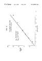
- FIG. 2is a transmission line measurement of the resistance in ohms vs. contact spacing in microns on the semiconductor-metal interface to a buried non-alloyed ohmic contact using a Be delta-doped Al 0.16 Ga 0.84 As monolayer;
- FIGS. 3A-3Care cross-sectional views illustrating a method for making the semiconductor device of FIG. 1;
- FIG. 4is a cross-sectional view through a second type of semiconductor device having a non-alloyed ohmic contact to a buried doped semiconductor layer;
- FIGS. 5A-5Eare cross-sectional views illustrating a method for making the semiconductor device of FIG. 4 ;
- FIG. 1shows a multilayer semiconductor device 10 having a non-alloyed ohmic contact to a buried doped semiconductor layer.
- the semiconductor device 10comprises a modulator based on III-V semiconductor material such as AlGaAs.
- the modulator 10includes a buried doped layer 12 of n or p AlGaAs followed by a chemically selective delta-doped stop-etch layer 14 .
- the delta-doped stop-etch layeris composed of a layer of n or p semiconductor material such as InGaP and a delta-doped monolayer or dopant sheet 16 disposed about 25 ⁇ below the stop-etch layer's 14 surface.
- the monolayer 16can be comprised of a dopant such as Be.
- This type of dopingprovides an increased amount of dopant in a single atomic plane or monolayer of the crystal.
- a plurality of AlGaAs layers formed in a mesa structure 18are disposed over a portion of the delta-doped stop-etch layer 14 .
- the layersconsist of a lightly doped n or p layer 20 , a lightly doped p or n layer 22 and a delta-doped p or n layer 24 having a second delta-doped Be monolayer 25 disposed about 25 ⁇ below the layer's 24 surface.
- the lightly doped layers 20 , 22define an electroabsorptive region 26 therebetween.
- a mirror 28 formed by Au or Au capped Ag film(about 200 nm to about 1000 nm thick) is disposed on the delta-doped layer 24 .
- the mirror 28 in the presence of the underlying delta-doped monolayer 25forms a self-aligned non-alloyed ohmic contact.
- a buried contact 30 formed by a second non-alloyed metal filmis disposed on the delta-doped stop-etch layer 14 to provide contact to the buried doped layer 12 .
- the buried non-alloyed contact 30is also ohmic because of the presence of the delta-doped monolayer 16 just under the surface of the delta-doped stop-etch layer 14 .
- the metal film of the buried contact 30is about 200 nm to about 1000 nm thick and can be formed from Ti, Au, Ag, Pt or combinations well known to those skilled in the art.
- the tunneling barrier tis thin (t ⁇ z D ) and hence, quantum-mechanical tunneling through the barrier provides the dominant transport mechanism.
- the minimized tunneling distancetherefore, advantageously lowers the contact resistance.
- the delta-doped monolayercreates a reservoir of electrons at a distance t from the metal-to-semiconductor interface. A major fraction of these electrons which originate from donors of the delta-doped monolayer occupy surface states at the metal-semiconductor interface.
- delta-doped monolayers 16 , 25 underneath the metal films 28 , 30advantageously results in lower resistance contacts which do not require alloying. This substantially reduces the amount of heat the device is subjected to during semiconductor processing thus, maintaining the reflectivity and reliability of the mirror 28 .
- additional delta-doped layerscan be provided under each metal film.
- Additional delta-doped layers provided under the metal mirror film 28can each include a p or n layer of AlGaAs and a delta-doped monolayer of Be.
- Additional delta-doped layers provided under the buried contact film 30can each include a p or n layer of AlGaAs (disposed under the delta-doped stop-etch layer 14 ) and a delta-doped monolayer of Be.
- FIG. 2is a transmission line measurement (TLM) that demonstrates the buried non-alloyed ohmic contact of the present invention using Be doping in Al 0.16 Ga 0.84 As.
- TLMtransmission line measurement
- This measurementwas accomplished by forming the semiconductor structure shown in FIG. 1 by etching down to the stop-etch layer 14 to expose its surface.
- a TLM structureconsisting of a line of variably spaced metal pads were photolithography formed by deposition of Au onto the surface of the stop-etch layer 14 followed by lift-off. Each metal pad was similar to the pad 30 shown in FIG. 1 .
- TLM structuresare well known in the semiconductor art for performing TLM measurements.
- the TLM structurewould be alloyed by heating if the conventional alloyed ohmic contacts are desired to be measured.
- FIG. 2shows the resistance measurement obtained on the non-alloyed TLM structure.
- the ohmic contactexhibited a sheet resistance R SHEET of 505 ohm per square and a contact resistance of R CONTACT of 5 ⁇ 10 ⁇ 5 ohm cm 2 . This very low contact resistance contributes minimally to the overall resistance of the semiconductor device.
- FIGS. 3A-3Cillustrate a method for fabricating the modulator device 10 shown in FIG. 1 .
- the first step shown in FIG. 3Aincludes forming the delta-doped stop etch layer 14 over the buried doped layer 12 .
- Methods for producing delta-doped layers in III-V semiconductor materialsare well known in the art. One such method is described in U.S. Pat. No. 5,013,685 to Chiu et al.
- the lightly doped layers 20 , 22 and the delta-doped layer 24are sequentially formed over the delta-doped stop-etch layer 14 and the device is then cooled to about room temperature.
- the non-alloyed mirror metal film 28 of Au or Au capped Agis then deposited directly on the cooled surface of the delta-doped layer 24 . This is performed even though the surface of the uppermost delta-doped layer 24 is exposed to atmosphere. However, measures are taken to minimize the presence of substantial oxide at the semiconductor-metal interface.
- the next step shown in FIG. 3Bincludes patterning the mirror film 28 into an etch mask. This can be accomplished using photolithography.
- the step shown in FIG. 3Cincludes etching the unmasked portions of the layers above the buried doped layer.
- the stop-etch layerstops the etching process approximately 25 ⁇ from the top of the delta-doped monolayer.
- the final stepincludes cooling the device to about room temperature and selectively depositing the second non-alloyed metal film on the cooled surface of the stop-etch layer 14 to form the non-alloyed ohmic contact 30 to the buried doped layer as shown in FIG. 1 .
- This stepis also performed so as to minimize the presence of substantial oxide at the semiconductor-metal interface. Because the metal film of the buried contact 30 does not need to be alloyed by heating the device, the reflectivity and reliability of the earlier formed mirror film 28 is maintained.
- All the semiconductor layers formed in the above stepscan be deposited using molecular beam epitaxy (MBE).
- MBEmolecular beam epitaxy
- the metal filmscan also be deposited using MBE.
- FIG. 4shows a multilayer laser semiconductor device 40 based on III-V AlGaAs semiconductor material.
- the laser 40includes a buried delta-doped layer 42 of n or p AlGaAs disposed on a plurality of semiconducting layers which form a bottom mirror stack 44 .
- the buried doped layer 42includes a delta-doped monolayer 46 disposed about 25 ⁇ below the buried doped layer's 42 surface.
- a plurality of semiconductor layers 48 formed in a mesa structureare disposed over a portion of the buried delta-doped layer 42 .
- the layers 48consist of a chemically selective n or p stop-etch layer 50 such as InGaP, a lightly doped AlGaAs n or p layer 52 , a plurality of AlGaAs p or n layers 54 which form an upper mirror stack, and a delta-doped AlGaAs p or n monolayer 56 .
- the lightly doped n or p layer 52 and the upper mirror stack 54define a gain region 58 .
- a mirror 60 formed by Au or Au capped Ag film(about 200 nm to about 1000 nm thick) is disposed on the delta-doped layer 56 .
- a delta-doped monolayer 57 under the metal mirror film 60provides a self-aligned non-alloyed ohmic contact.
- the contact 62is about 200 nm to about 1000 nm thick and is also ohmic because of the presence of the delta-doped monolayer 46 .
- FIGS. 5A-5Eillustrate a method for fabricating the laser device 40 shown in FIG. 4 .
- the first step shown in FIG. 5Aincludes forming the buried delta-doped layer 42 the delta-doped monolayer 46 about 25 ⁇ below the layer's surface.
- the next step shown in FIG. 5Bincludes depositing the stop-etch layer 50 on top of the buried delta-doped layer 42 .
- the lightly doped layer 52 , the layers of upper mirror stack 54 , and the delta-doped layer 56are sequentially formed over the stop etch layer 50 and the device is then cooled to about room temperature.
- the non-alloyed metal mirror film 60is deposited directly on the cooled surface of the delta-doped layer 56 . This is performed even though the surface of the delta-doped layer 56 is exposed to atmosphere. However, measures are taken to minimize the presence of substantial oxide at the semiconductor-metal interface.
- the step shown in FIG. 5Cincludes patterning the mirror film 60 into an etch mask using photolithography.
- the step shown in FIGS. 5D and 5Eincludes etching the unmasked layers above the buried doped layer 42 . This is performed with two etching steps.
- the first etching step shown in FIG. 5Dis controlled by the stop-etch layer 50 and results in the removal of all the unmasked layers above the stop-etch layer 50 .
- the second etching step shown in FIG. 5Eselectively removes the unmasked portion of the stop-etch layer 50 thereby leaving the delta-doped monolayer 46 about 25 ⁇ below the surface of the buried doped layer 42 .
- the final stepincludes cooling the device to about room temperature and epitaxially depositing the second non-alloyed metal film on the cooled surface of the buried doped layer 42 to form the non-alloyed ohmic contact 62 to the buried doped layer 42 as shown in FIG. 4 .
- This stepis also performed so to minimize the presence of substantial oxide at the semiconductor-metal interface.
Landscapes
- Physics & Mathematics (AREA)
- Condensed Matter Physics & Semiconductors (AREA)
- General Physics & Mathematics (AREA)
- Electromagnetism (AREA)
- Optics & Photonics (AREA)
- Electrodes Of Semiconductors (AREA)
Abstract
Description
Claims (19)
Priority Applications (1)
| Application Number | Priority Date | Filing Date | Title |
|---|---|---|---|
| US09/083,165US6258616B1 (en) | 1998-05-22 | 1998-05-22 | Method of making a semiconductor device having a non-alloyed ohmic contact to a buried doped layer |
Applications Claiming Priority (1)
| Application Number | Priority Date | Filing Date | Title |
|---|---|---|---|
| US09/083,165US6258616B1 (en) | 1998-05-22 | 1998-05-22 | Method of making a semiconductor device having a non-alloyed ohmic contact to a buried doped layer |
Publications (1)
| Publication Number | Publication Date |
|---|---|
| US6258616B1true US6258616B1 (en) | 2001-07-10 |
Family
ID=22176602
Family Applications (1)
| Application Number | Title | Priority Date | Filing Date |
|---|---|---|---|
| US09/083,165Expired - LifetimeUS6258616B1 (en) | 1998-05-22 | 1998-05-22 | Method of making a semiconductor device having a non-alloyed ohmic contact to a buried doped layer |
Country Status (1)
| Country | Link |
|---|---|
| US (1) | US6258616B1 (en) |
Cited By (4)
| Publication number | Priority date | Publication date | Assignee | Title |
|---|---|---|---|---|
| US6654604B2 (en)* | 2000-11-21 | 2003-11-25 | Matsushita Electric Industrial Co. Ltd. | Equipment for communication system |
| RU2394305C2 (en)* | 2007-07-20 | 2010-07-10 | Гэлиэм Энтерпрайзис Пти Лтд | Semiconductor device with built-in contacts (versions) and method of making semiconductor devices with built-in contacts (versions) |
| WO2019212576A1 (en)* | 2018-05-01 | 2019-11-07 | Facebook Technologies, Llc | Micron-sized light emitting diode designs |
| US20220247153A1 (en)* | 2019-11-06 | 2022-08-04 | Sony Semiconductor Solutions Corporation | Surface light-emission laser device |
Citations (11)
| Publication number | Priority date | Publication date | Assignee | Title |
|---|---|---|---|---|
| US4772934A (en)* | 1986-06-06 | 1988-09-20 | American Telephone And Telegraph Company, At&T Bell Laboratories | Delta-doped ohmic metal to semiconductor contacts |
| US4784967A (en)* | 1986-12-19 | 1988-11-15 | American Telephone And Telegraph Company, At&T Bell Laboratories | Method for fabricating a field-effect transistor with a self-aligned gate |
| US4789645A (en)* | 1987-04-20 | 1988-12-06 | Eaton Corporation | Method for fabrication of monolithic integrated circuits |
| US4794445A (en)* | 1986-07-31 | 1988-12-27 | Hitachi, Ltd. | Semiconductor device |
| US4882609A (en)* | 1984-11-19 | 1989-11-21 | Max-Planck Gesellschaft Zur Forderung Der Wissenschafter E.V. | Semiconductor devices with at least one monoatomic layer of doping atoms |
| US5004705A (en)* | 1989-01-06 | 1991-04-02 | Unitrode Corporation | Inverted epitaxial process |
| US5013685A (en) | 1989-11-02 | 1991-05-07 | At&T Bell Laboratories | Method of making a non-alloyed ohmic contact to III-V semiconductors-on-silicon |
| US5700349A (en)* | 1995-01-20 | 1997-12-23 | Sony Corporation | Method for forming multi-layer interconnections |
| US5856700A (en)* | 1996-05-08 | 1999-01-05 | Harris Corporation | Semiconductor device with doped semiconductor and dielectric trench sidewall layers |
| US5895953A (en)* | 1994-11-09 | 1999-04-20 | Harris Corporation | Ohmic contact to lightly doped islands from a conductive rapid diffusion buried layer |
| US5932898A (en)* | 1996-04-01 | 1999-08-03 | Delco Electronics Corporation | Integrated inductive load snubbing device |
- 1998
- 1998-05-22USUS09/083,165patent/US6258616B1/ennot_activeExpired - Lifetime
Patent Citations (11)
| Publication number | Priority date | Publication date | Assignee | Title |
|---|---|---|---|---|
| US4882609A (en)* | 1984-11-19 | 1989-11-21 | Max-Planck Gesellschaft Zur Forderung Der Wissenschafter E.V. | Semiconductor devices with at least one monoatomic layer of doping atoms |
| US4772934A (en)* | 1986-06-06 | 1988-09-20 | American Telephone And Telegraph Company, At&T Bell Laboratories | Delta-doped ohmic metal to semiconductor contacts |
| US4794445A (en)* | 1986-07-31 | 1988-12-27 | Hitachi, Ltd. | Semiconductor device |
| US4784967A (en)* | 1986-12-19 | 1988-11-15 | American Telephone And Telegraph Company, At&T Bell Laboratories | Method for fabricating a field-effect transistor with a self-aligned gate |
| US4789645A (en)* | 1987-04-20 | 1988-12-06 | Eaton Corporation | Method for fabrication of monolithic integrated circuits |
| US5004705A (en)* | 1989-01-06 | 1991-04-02 | Unitrode Corporation | Inverted epitaxial process |
| US5013685A (en) | 1989-11-02 | 1991-05-07 | At&T Bell Laboratories | Method of making a non-alloyed ohmic contact to III-V semiconductors-on-silicon |
| US5895953A (en)* | 1994-11-09 | 1999-04-20 | Harris Corporation | Ohmic contact to lightly doped islands from a conductive rapid diffusion buried layer |
| US5700349A (en)* | 1995-01-20 | 1997-12-23 | Sony Corporation | Method for forming multi-layer interconnections |
| US5932898A (en)* | 1996-04-01 | 1999-08-03 | Delco Electronics Corporation | Integrated inductive load snubbing device |
| US5856700A (en)* | 1996-05-08 | 1999-01-05 | Harris Corporation | Semiconductor device with doped semiconductor and dielectric trench sidewall layers |
Cited By (10)
| Publication number | Priority date | Publication date | Assignee | Title |
|---|---|---|---|---|
| US6654604B2 (en)* | 2000-11-21 | 2003-11-25 | Matsushita Electric Industrial Co. Ltd. | Equipment for communication system |
| US6940127B2 (en) | 2000-11-21 | 2005-09-06 | Matsushita Electric Industrial Co., Ltd. | Equipment for communication system and semiconductor integrated circuit device |
| RU2394305C2 (en)* | 2007-07-20 | 2010-07-10 | Гэлиэм Энтерпрайзис Пти Лтд | Semiconductor device with built-in contacts (versions) and method of making semiconductor devices with built-in contacts (versions) |
| WO2019212576A1 (en)* | 2018-05-01 | 2019-11-07 | Facebook Technologies, Llc | Micron-sized light emitting diode designs |
| US10483430B1 (en) | 2018-05-01 | 2019-11-19 | Facebook Technologies, Llc | Micron-sized light emitting diode designs |
| US10847675B2 (en) | 2018-05-01 | 2020-11-24 | Facebook Technologies, Llc | Micron-sized light emiting diode designs |
| JP2021521644A (en)* | 2018-05-01 | 2021-08-26 | フェイスブック・テクノロジーズ・リミテッド・ライアビリティ・カンパニーFacebook Technologies, Llc | Micron size light emitting diode design |
| US11342483B2 (en) | 2018-05-01 | 2022-05-24 | Facebook Technologies, Llc | Micron-sized light emitting diode designs |
| JP7284188B2 (en) | 2018-05-01 | 2023-05-30 | メタ プラットフォームズ テクノロジーズ, リミテッド ライアビリティ カンパニー | Micron size light emitting diode design |
| US20220247153A1 (en)* | 2019-11-06 | 2022-08-04 | Sony Semiconductor Solutions Corporation | Surface light-emission laser device |
Similar Documents
| Publication | Publication Date | Title |
|---|---|---|
| US6229153B1 (en) | High peak current density resonant tunneling diode | |
| EP0426380B1 (en) | Non-alloyed ohmic contact to III-V semiconductors-on-silicon | |
| JPH0752724B2 (en) | Method for forming ohmic contacts in a semiconductor device | |
| JP3210657B2 (en) | Heterojunction bipolar transistor | |
| US6258616B1 (en) | Method of making a semiconductor device having a non-alloyed ohmic contact to a buried doped layer | |
| JP4048284B2 (en) | Laminate for forming ohmic electrode and ohmic electrode | |
| JPH08181335A (en) | Lateral resonant tunneling | |
| US5047832A (en) | Electrode structure for III-V compound semiconductor element and method of manufacturing the same | |
| EP0420322B1 (en) | Process for manufacturing a semiconductor integrated circuit including a heterojunction bipolar transistor and/or buried resistors | |
| JP2000307190A (en) | Manufacturing method of surface emitting semiconductor laser | |
| KR100277398B1 (en) | Semiconductor laser | |
| EP0638937A2 (en) | Ohmic electrode, its fabricating method and semiconductor device using this electrode | |
| JP2652647B2 (en) | Heterojunction field effect transistor | |
| CN115224130B (en) | A high impedance semiconductor resistor structure and manufacturing method thereof | |
| JP2654828B2 (en) | Semiconductor device having quantum wires and method of manufacturing the same | |
| JP2817217B2 (en) | Semiconductor device having metal / semiconductor junction and method of manufacturing the same | |
| US5629215A (en) | Method of fabricating and contacting ultra-small three terminal semiconductor devices | |
| JPH0773138B2 (en) | Method for manufacturing III-V group semiconductor laser | |
| JP2950712B2 (en) | Method for manufacturing semiconductor device | |
| JP3876397B2 (en) | Method for manufacturing a Group III-V Group compound semiconductor device | |
| JP2844995B2 (en) | Field effect transistor and method for manufacturing the same | |
| JP4147441B2 (en) | Compound semiconductor device | |
| JP3244795B2 (en) | Method for manufacturing semiconductor device | |
| JP2844994B2 (en) | Method for manufacturing field effect transistor | |
| JP3295897B2 (en) | Semiconductor device and manufacturing method thereof |
Legal Events
| Date | Code | Title | Description |
|---|---|---|---|
| STCF | Information on status: patent grant | Free format text:PATENTED CASE | |
| FEPP | Fee payment procedure | Free format text:PAYOR NUMBER ASSIGNED (ORIGINAL EVENT CODE: ASPN); ENTITY STATUS OF PATENT OWNER: LARGE ENTITY Free format text:PAYER NUMBER DE-ASSIGNED (ORIGINAL EVENT CODE: RMPN); ENTITY STATUS OF PATENT OWNER: LARGE ENTITY | |
| FPAY | Fee payment | Year of fee payment:4 | |
| FPAY | Fee payment | Year of fee payment:8 | |
| FPAY | Fee payment | Year of fee payment:12 | |
| AS | Assignment | Owner name:DEUTSCHE BANK AG NEW YORK BRANCH, AS COLLATERAL AG Free format text:PATENT SECURITY AGREEMENT;ASSIGNORS:LSI CORPORATION;AGERE SYSTEMS LLC;REEL/FRAME:032856/0031 Effective date:20140506 | |
| AS | Assignment | Owner name:AVAGO TECHNOLOGIES GENERAL IP (SINGAPORE) PTE. LTD Free format text:ASSIGNMENT OF ASSIGNORS INTEREST;ASSIGNOR:AGERE SYSTEMS LLC;REEL/FRAME:035365/0634 Effective date:20140804 | |
| AS | Assignment | Owner name:LSI CORPORATION, CALIFORNIA Free format text:TERMINATION AND RELEASE OF SECURITY INTEREST IN PATENT RIGHTS (RELEASES RF 032856-0031);ASSIGNOR:DEUTSCHE BANK AG NEW YORK BRANCH, AS COLLATERAL AGENT;REEL/FRAME:037684/0039 Effective date:20160201 Owner name:AGERE SYSTEMS LLC, PENNSYLVANIA Free format text:TERMINATION AND RELEASE OF SECURITY INTEREST IN PATENT RIGHTS (RELEASES RF 032856-0031);ASSIGNOR:DEUTSCHE BANK AG NEW YORK BRANCH, AS COLLATERAL AGENT;REEL/FRAME:037684/0039 Effective date:20160201 | |
| AS | Assignment | Owner name:BANK OF AMERICA, N.A., AS COLLATERAL AGENT, NORTH CAROLINA Free format text:PATENT SECURITY AGREEMENT;ASSIGNOR:AVAGO TECHNOLOGIES GENERAL IP (SINGAPORE) PTE. LTD.;REEL/FRAME:037808/0001 Effective date:20160201 Owner name:BANK OF AMERICA, N.A., AS COLLATERAL AGENT, NORTH Free format text:PATENT SECURITY AGREEMENT;ASSIGNOR:AVAGO TECHNOLOGIES GENERAL IP (SINGAPORE) PTE. LTD.;REEL/FRAME:037808/0001 Effective date:20160201 | |
| AS | Assignment | Owner name:AVAGO TECHNOLOGIES GENERAL IP (SINGAPORE) PTE. LTD., SINGAPORE Free format text:TERMINATION AND RELEASE OF SECURITY INTEREST IN PATENTS;ASSIGNOR:BANK OF AMERICA, N.A., AS COLLATERAL AGENT;REEL/FRAME:041710/0001 Effective date:20170119 Owner name:AVAGO TECHNOLOGIES GENERAL IP (SINGAPORE) PTE. LTD Free format text:TERMINATION AND RELEASE OF SECURITY INTEREST IN PATENTS;ASSIGNOR:BANK OF AMERICA, N.A., AS COLLATERAL AGENT;REEL/FRAME:041710/0001 Effective date:20170119 | |
| AS | Assignment | Owner name:AVAGO TECHNOLOGIES INTERNATIONAL SALES PTE. LIMITE Free format text:ASSIGNMENT OF ASSIGNORS INTEREST;ASSIGNOR:AVAGO TECHNOLOGIES GENERAL IP (SINGAPORE) PTE. LTD.;REEL/FRAME:047022/0620 Effective date:20180509 | |
| AS | Assignment | Owner name:AVAGO TECHNOLOGIES INTERNATIONAL SALES PTE. LIMITE Free format text:CORRECTIVE ASSIGNMENT TO CORRECT THE NATURE OF CONVEYANCE AND EFFECTIVE DATE PREVIOUSLY RECORDED ON REEL 047022 FRAME 0620. ASSIGNOR(S) HEREBY CONFIRMS THE MERGER;ASSIGNOR:AVAGO TECHNOLOGIES GENERAL IP (SINGAPORE) PTE. LTD.;REEL/FRAME:047185/0643 Effective date:20180509 | |
| AS | Assignment | Owner name:AVAGO TECHNOLOGIES INTERNATIONAL SALES PTE. LIMITE Free format text:CORRECTIVE ASSIGNMENT TO CORRECT THE EFFECTIVE DATE PREVIOUSLY RECORDED ON REEL 047185 FRAME 0643. ASSIGNOR(S) HEREBY CONFIRMS THE MERGER;ASSIGNOR:AVAGO TECHNOLOGIES GENERAL IP (SINGAPORE) PTE. LTD.;REEL/FRAME:047476/0845 Effective date:20180905 | |
| AS | Assignment | Owner name:AVAGO TECHNOLOGIES INTERNATIONAL SALES PTE. LIMITE Free format text:CORRECTIVE ASSIGNMENT TO CORRECT THE EFFECTIVE DATE OF MERGER PREVIOUSLY RECORDED AT REEL: 047185 FRAME: 0643. ASSIGNOR(S) HEREBY CONFIRMS THE CORRECTIVE MERGER;ASSIGNOR:AVAGO TECHNOLOGIES GENERAL IP (SINGAPORE) PTE. LTD.;REEL/FRAME:047959/0296 Effective date:20180905 |