US6258205B1 - Endpoint detection method and apparatus which utilize an endpoint polishing layer of catalyst material - Google Patents
Endpoint detection method and apparatus which utilize an endpoint polishing layer of catalyst materialDownload PDFInfo
- Publication number
- US6258205B1 US6258205B1US09/534,652US53465200AUS6258205B1US 6258205 B1US6258205 B1US 6258205B1US 53465200 AUS53465200 AUS 53465200AUS 6258205 B1US6258205 B1US 6258205B1
- Authority
- US
- United States
- Prior art keywords
- polishing
- wafer
- endpoint
- reagent
- layer
- Prior art date
- Legal status (The legal status is an assumption and is not a legal conclusion. Google has not performed a legal analysis and makes no representation as to the accuracy of the status listed.)
- Expired - Lifetime
Links
Images


Classifications
- B—PERFORMING OPERATIONS; TRANSPORTING
- B24—GRINDING; POLISHING
- B24B—MACHINES, DEVICES, OR PROCESSES FOR GRINDING OR POLISHING; DRESSING OR CONDITIONING OF ABRADING SURFACES; FEEDING OF GRINDING, POLISHING, OR LAPPING AGENTS
- B24B37/00—Lapping machines or devices; Accessories
- B24B37/04—Lapping machines or devices; Accessories designed for working plane surfaces
- B—PERFORMING OPERATIONS; TRANSPORTING
- B24—GRINDING; POLISHING
- B24B—MACHINES, DEVICES, OR PROCESSES FOR GRINDING OR POLISHING; DRESSING OR CONDITIONING OF ABRADING SURFACES; FEEDING OF GRINDING, POLISHING, OR LAPPING AGENTS
- B24B49/00—Measuring or gauging equipment for controlling the feed movement of the grinding tool or work; Arrangements of indicating or measuring equipment, e.g. for indicating the start of the grinding operation
- B—PERFORMING OPERATIONS; TRANSPORTING
- B24—GRINDING; POLISHING
- B24B—MACHINES, DEVICES, OR PROCESSES FOR GRINDING OR POLISHING; DRESSING OR CONDITIONING OF ABRADING SURFACES; FEEDING OF GRINDING, POLISHING, OR LAPPING AGENTS
- B24B55/00—Safety devices for grinding or polishing machines; Accessories fitted to grinding or polishing machines for keeping tools or parts of the machine in good working condition
- B24B55/12—Devices for exhausting mist of oil or coolant; Devices for collecting or recovering materials resulting from grinding or polishing, e.g. of precious metals, precious stones, diamonds or the like
- B—PERFORMING OPERATIONS; TRANSPORTING
- B24—GRINDING; POLISHING
- B24B—MACHINES, DEVICES, OR PROCESSES FOR GRINDING OR POLISHING; DRESSING OR CONDITIONING OF ABRADING SURFACES; FEEDING OF GRINDING, POLISHING, OR LAPPING AGENTS
- B24B57/00—Devices for feeding, applying, grading or recovering grinding, polishing or lapping agents
- B24B57/02—Devices for feeding, applying, grading or recovering grinding, polishing or lapping agents for feeding of fluid, sprayed, pulverised, or liquefied grinding, polishing or lapping agents
- H—ELECTRICITY
- H01—ELECTRIC ELEMENTS
- H01L—SEMICONDUCTOR DEVICES NOT COVERED BY CLASS H10
- H01L21/00—Processes or apparatus adapted for the manufacture or treatment of semiconductor or solid state devices or of parts thereof
- H01L21/02—Manufacture or treatment of semiconductor devices or of parts thereof
- H01L21/04—Manufacture or treatment of semiconductor devices or of parts thereof the devices having potential barriers, e.g. a PN junction, depletion layer or carrier concentration layer
- H01L21/18—Manufacture or treatment of semiconductor devices or of parts thereof the devices having potential barriers, e.g. a PN junction, depletion layer or carrier concentration layer the devices having semiconductor bodies comprising elements of Group IV of the Periodic Table or AIIIBV compounds with or without impurities, e.g. doping materials
- H01L21/30—Treatment of semiconductor bodies using processes or apparatus not provided for in groups H01L21/20 - H01L21/26
- H01L21/31—Treatment of semiconductor bodies using processes or apparatus not provided for in groups H01L21/20 - H01L21/26 to form insulating layers thereon, e.g. for masking or by using photolithographic techniques; After treatment of these layers; Selection of materials for these layers
- H01L21/3105—After-treatment
- H01L21/31051—Planarisation of the insulating layers
- H01L21/31053—Planarisation of the insulating layers involving a dielectric removal step
Definitions
- the present inventionrelates generally to an endpoint detection method and apparatus, and more particularly to method and apparatus that polish a semiconductor wafer down to a polishing endpoint layer that contains catalyst material.
- Semiconductor integrated circuitsare typically fabricated by a layering process in which several layers of material are fabricated (i) on or in a surface of a wafer, or (ii) on a surface of a previous layer.
- This fabrication processvery often requires layers to be fabricated upon a smooth, planar surface of a previous layer.
- the surface topography of layersmay be highly uneven due to (i) areas which are higher than the remainder of the surface or (ii) an uneven topography of an underlying layer.
- a layermay need to be polished so as to present a smooth planar surface for the next processing step, such as formation of a conductor layer or pattern on the surface of another layer.
- a semiconductor wafermay be polished to remove high topography and surface defects such as crystal lattice damage, scratches, roughness, or embedded particles of dirt or dust.
- the polishing processtypically is accomplished with a polishing system that includes top and bottom platens (e.g. a polishing table and a wafer carrier or holder), between which the semiconductor wafer is positioned. The platens are moved relative to each other thereby causing material to be removed from the surface of the wafer.
- This polishing processis often referred to as mechanical planarization (MP) and is utilized to improve the quality and reliability of semiconductor devices.
- the polishing processmay also involve the introduction of a chemical slurry to facilitate (i) higher removal rates, and (ii) selective removal of materials fabricated upon the semiconductor wafer. This polishing process is often referred to as chemical mechanical planarization or chemical mechanical polishing (CMP).
- a typical method employed for determining endpoint in polishing systemsis to measure the amount of time needed to planarize a first wafer, and then to run the remaining wafers for similar times. In practice this method is extremely time consuming, since operators must inspect each wafer after polishing. This is because it is extremely difficult to precisely control the removal rate of material since the removal rate may vary during the polishing of an individual wafer or because the removal rate may diminish in the process of polishing a number of wafers in sequence.
- Another method employed for determining endpoint in polishing systemsis to (i) form a polishing endpoint layer in the semiconductor device, and (ii) polish the semiconductor device down to the polishing endpoint layer.
- polishing systemsdetect when the polishing process reaches the polishing endpoint layer and terminate the polishing process in response to reaching the polishing endpoint layer.
- Various techniqueshave been used to detect when the polishing process reaches the polishing endpoint layer. For example, U.S. Pat. No. 5,668,063 to Fry et al polishes a semiconductor device down to a tracer layer of detectable material. The polishing system of Fry determines that the tracer layer has been reached when a chemical element detector detects materials such as boron or phosphorous of the tracer layer have been removed by the polishing process.
- the chemical element detectorIn order to base endpoint detection upon detecting material of the tracer layer, the chemical element detector needs to accurately detect rather small amounts of the tracer layer material, or the polishing system needs to remove more of the tracer layer material in order to provide the chemical element detector with enough material for accurate detection.
- the material of the tracer layeris consumed as a reagent of a chemical reaction to be detected by the detector. In this case, the detector would need to be able to detect the effect of a small reaction, or the polishing system would need to remove more of the tracer layer in order to provide enough tracer material for a substantial reaction to occur.
- Detectors capable of detecting small amounts of the tracer layer or detecting the effect of a small chemical reactionare more expensive than detectors capable of detecting larger amounts of the tracer layer or detecting the effect of a larger chemical reaction. Furthermore, the additional removal of the tracer layer in order to provide more tracer layer material for detection increases the risk of overpolishing especially when the topography of the tracer layer is highly uneven.
- a method of planarizing a semiconductor wafer having a polishing endpoint layer that includes a catalyst materialincludes polishing a first side of the wafer in order to remove material from the wafer.
- Another step of the methodincludes determining that a catalytic reaction has occurred due to the polishing step removing the catalyst material of the polishing endpoint layer.
- the methodalso includes the step of terminating the polishing step in response to determining that the catalytic reaction has occurred.
- a method of planarizing a semiconductor wafer down to a predetermined distance from a semiconductor substrate of the waferincludes forming in the wafer a catalyst material that is at the predetermined distance from the substrate of the wafer. Another step of the method includes polishing a first side of the wafer in order to remove material from the wafer. The method also includes the step of determining that a catalytic reaction has occurred due to the polishing step removing a portion of the catalyst material from the wafer. Moreover, the method includes the step of terminating the polishing step in response to determining that the catalytic reaction has occurred.
- an apparatus for polishing a semiconductor wafer down to a catalyst material of the waferincludes a polishing platen having a polishing surface, a wafer carrier, a slurry supply system, and a polishing endpoint detector.
- the wafer carrieris configured to (i) engage the wafer by the second side of the wafer and (ii) press the first side of the wafer against the polishing surface of the polishing platen.
- the slurry supply systemis configured to apply a chemical slurry to the first side of the wafer which (i) facilities removal of material from the wafer, and (ii) receives the material removed from the wafer carrier.
- the polishing platen and the wafer carrierare configured to rub the first side of the wafer against the polishing surface in the presence of the chemical slurry in order to remove the material from the wafer.
- the polishing endpoint detectoris operable to (i) detect based upon the chemical slurry whether a catalytic reaction has occurred due to the polishing platen removing a portion of the catalyst material from the wafer. Moreover, the polishing endpoint detector is operable to cause the polishing of the wafer to terminate in response to detecting the catalytic reaction.
- FIGS. 1A-1Fshow sectional views of a semiconductor wafer during various steps of a fabrication process
- FIG. 2shows an embodiment of a polishing system which incorporates various features of the present invention therein;
- FIG. 3shows a flowchart of a polishing procedure used by the polishing system of FIG. 2 .
- FIGS. 1A-1Fillustrate sectional views of a semiconductor wafer 100 after various steps of a fabrication process of the present invention.
- FIGS. 1A-1Fillustrate planarizafion of a semiconductor 100 down to a polishing endpoint layer 118 .
- FIG. 1Ashows the semiconductor wafer 100 after a number of fabrication steps.
- the semiconductor wafer 100includes a semiconductor substrate 102 upon which a fabrication process formed a first insulating layer 104 and a first metal layer 106 .
- the fabrication processformed the first insulating layer 104 upon the semiconductor substrate 102 , and a contact hole 108 in the first insulating layer 104 at a location above a transistor portion (not shown) of the semiconductor substrate 102 .
- the fabrication processpatterned the first metal layer 106 (e.g. aluminum) over the first insulating layer 104 and the contact hole 108 .
- the first metal layer 106fills the contact hole 108 forming an electrical contact with the transistor portion of the semiconductor substrate 102 .
- the filling of the contact hole 108forms a pit 110 in the portion of the first metal layer 106 lying above the contact hole 108 .
- the semiconductor wafer 100is shown in FIG. 1B after the fabrication process formed a second insulating layer 112 upon the surface of the semiconductor wafer 100 .
- the second insulating layer 112has a highly uneven surface topography.
- the uneven surface topography of the second insulating layer 112would cause accuracy problems in fabricating additional layers of the semiconductor wafer 100 .
- the uneven surface topographywould cause control problems for a lithography process used to pattern a second metal layer 120 (FIG. 1F) upon the second insulating layer 112 .
- a polishing systemsuch as the polishing system 210 of FIG. 2 polishes the second insulating layer 112 down to a first level 116 , thus planarizing the surface of the second insulating layer 112 .
- the fabrication processimplants a polishing endpoint layer 118 into the second insulating layer 112 .
- the polishing endpoint layer 118 in the present inventionincludes a catalyst material which the polishing system 210 uses in determining a polishing endpoint.
- the implanted polishing endpoint layer 118starts at the first level 116 and ends at a second level 120 that lies above the first metal layer 106 .
- Methods of ion implanting material into a semiconductor waferare well known in the art. Accordingly, ion implantation techniques are not described herein.
- implantation techniquesdistribute the implanted material at various depths from the surface of implantation with a peak distribution occurring at the desired depth. Accordingly, implantation techniques implant some material at a depth greater than the desired depth and implant some material at a depth less than the desired depth. Since implantation of the material into underlying layers may result in reliability problems, the implantation technique should ensure that the underlying layers such as the first metal layer 106 are not contaminated with the implanted material.
- the polishing system 210utilizes the implanted material of the polishing endpoint layer 118 to determine the polishing endpoint, the implantation technique should implant the material of the polishing endpoint layer 118 such that the polishing endpoint layer 118 starts below a second level 122 that corresponds to the lowest part of the surface to be planarized.
- the implantation techniquealso tends to create a non-planar polishing endpoint layer 118 due to the uneven surface topography of the second insulating layer 112 . Since the implantation technique implants the material of the polishing endpoint layer 118 through the surface of the second insulating layer 112 , the implanted polishing endpoint layer 118 generally follows the topography of the second insulating layer 112 . As a result, the implantation technique needs to account for the uneven topography of the second insulating layer 112 when determining the desired depth of the implanted polishing endpoint layer 118 .
- polishing the second insulating layer 112 prior to implanting the polishing endpoint layer 118generally generates a more planar polishing endpoint layer 118 , thus making it easier to implant a polishing endpoint layer 118 which is (i) deep enough to cause the polishing system 210 to planarize the semiconductor wafer 100 , and (ii) not deep enough to cause the implantation technique to contaminate underlying layers with implanted material.
- FIG. 1Dshows the semiconductor wafer 100 after the polishing system 210 has polished the semiconductor wafer 100 down to the polishing endpoint layer 118 .
- the semiconductor wafer 100has a planar surface upon which additional layers may be fabricated.
- the fabrication processmay etch a via 126 through the second insulating layer 112 and the polishing endpoint layer 118 (FIG. 1 E). Then, the fabrication process may pattern a second metal layer 120 upon the second insulating layer 112 and the polishing endpoint layer 118 as shown in FIG. 1 F.
- the fabrication processmay need to form a third insulating layer upon the planarized surface prior to forming the additional layer in order to insulate the additional layer from the polishing endpoint layer 118 .
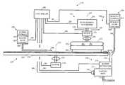
- the polishing system 210includes a platen motor or other drive mechanism 218 and platen subassembly 220 .
- the platen motor 218rotates the platen subassembly 220 about a center axis 222 at a platen velocity V p .
- the platen motor 218may rotate the platen subassembly 220 in a clockwise direction as shown by arrow 224 or in the counterclockwise direction.
- the platen subassembly 220includes a polishing platen 226 and polishing pad 228 mounted upon the polishing platen 226 . Both the polishing platen 226 and the polishing pad 228 are preferably circular and define a polishing surface against which the polishing system 210 may polish the semiconductor wafer 100 . Moreover, the polishing pad 228 is typically made of blown polyurethane which protects the polishing platen 226 from chemical slurry and other chemicals introduced during the polishing process.
- the polishing system 210also includes a polishing head subassembly 230 .
- the polishing head subassembly 230includes a wafer carrier 232 , a cooling mechanism 233 , a carrier motor or other drive mechanism 234 , and a wafer carrier displacement mechanism 236 .
- the wafer carrier 232applies a controlled adjustable downward force F (as illustrated by arrow 238 ) to press semiconductor wafer 100 into polishing pad 228 to facilitate polishing of the front side of the semiconductor wafer 100 .
- the carrier motor 234rotates wafer carrier 232 and semiconductor wafer 100 about a center axis 237 at a wafer velocity V w .
- the carrier wafermay rotate the wafer carrier 232 in a clockwise direction as shown by arrow 235 or in the counterclockwise direction.
- the carrier motor 234preferably rotates the wafer carrier 232 in the same rotational direction as platen motor 218 rotates the platen subassembly 220 (although the carrier motor 234 may rotate the semiconductor wafer 100 in the rotational direction opposite the rotational direction of the platen subassembly 220 as desired).
- the wafer carrier 232also includes mechanisms (not shown) for holding the semiconductor wafer 100 .
- the wafer carrier 232may include a vacuum-type mechanism which generates a vacuum force that draws the semiconductor wafer 100 against the wafer carrier 232 .
- the vacuum forcemay be removed.
- the wafer carrier 232may be designed with a friction surface or a carrier pad which engages the back side of the semiconductor wafer 100 .
- the carrier pad and downward force Fcreate a frictional force between the wafer carrier 232 and the semiconductor wafer 100 that effectively holds the semiconductor wafer 100 against the wafer carrier 232 and causes the semiconductor wafer 100 to rotate at the same velocity as the wafer carrier 232 .
- Such wafer carriers and carrier padsare of conventional design and are commercially available.
- the cooling mechanism 233counteracts heat generated during the polishing process in order to maintain the wafer carder 232 at a substantially constant temperature.
- the cooling mechanismneutralizes the heat generated due to (i) friction and (ii) the chemical slurry reacting with the front side of the semiconductor wafer 100 .
- the displacement mechanism 236moves the wafer carrier 232 and the semiconductor wafer 100 under a controlled force F across the platen subassembly 220 as indicated by arrows 231 and 239 .
- the semiconductor wafer 100is moved at an adjustable rate and along a variable polishing path P.
- the polishing path Pmay be linear, sinusoidal, or a variety of other patterns.
- the wafer carrier displacement mechanism 236is also capable of moving the semiconductor wafer 100 along a polishing path to a location beyond the edge of the polishing pad 228 so that the semiconductor wafer 100 “overhangs” the edge.
- This overhang arrangementpermits the semiconductor wafer 100 to be moved partially on and partially off the polishing pad 228 to compensate for polishing irregularities caused by a relative velocity differential between the faster moving outer portions and the slower moving inner portions of the platen subassembly 220 .
- the polishing system 210also includes a reagent supply system 240 and a chemical supply system 260 .
- the reagent supply system 240includes a reagent storage 242 , a reagent flow control mechanism 244 , and a reagent conduit 246 .
- the reagent storage 242includes one or more containers for storing reagents.
- the reagent storage 242stores reagents which react in the presence of the catalyst material of the polishing endpoint layer 118 .
- the reagent storage 242may store t-butyl bromide (i.e. (CH 3 ) 3 CBr) which catalytically reacts with water (i.e. H 2 O) in the presence of silver ions (i.e.
- reagent and catalyst materialare merely exemplary and that many other reagents and catalyst materials may be suitable for use with the polishing system 210 .
- t-butyl bromidemay be replaced with a hydrocarbon of similar stereochemistry that is similarly halogenated and the silver ions may be replaced with mercury ions (i.e. Hg 2+ ).
- the reagent flow control mechanism 244controls the flow of reagent through the reagent conduit 246 , and the reagent conduit 246 connects the reagent supply system 240 to the extraction conduit 272 of the endpoint detector 270 (discussed below) so that reagent may be transferred from the reagent supply system 240 to the testing area 274 of the endpoint detector 270 .
- the reagent flow control mechanism 244 and the reagent conduit 246transfer reagent from the reagent storage 242 to the extraction conduit 272 at a reagent flow rate ⁇ R such as 0.5 moles a second of reagent (e.g. t-butyl bromide) for 1-10 cubic centimeters a second (ccls) of effluent flowing through the extraction conduit 272 .
- the slurry supply system 260includes a slurry storage 262 , a slurry flow control mechanism 264 , and a slurry conduit 266 .
- the reagent storage 262includes one or more containers for storing slurry.
- the slurry storage 262stores a slurry that includes alumina (i.e. AlO 3 ) which is an abrasive material that facilitates polishing of the front side of the semiconductor wafer 100 and reactants which selectively react to certain materials of the front side of the semiconductor wafer 100 . Chemical slurries having such properties are well known and commercially available.
- the slurry stored in the slurry storage 262is sufficiently acidic to dissolve silver ions of the polishing endpoint layer 118 .
- the polishing system 210may be constructed without the reagent supply system 240 if the reagents are included in the chemical slurry of the slurry supply system 260 .
- the slurry flow control mechanism 260controls the flow of slurry through the slurry conduit 266 , and the slurry conduit 256 transfers the slurry from the slurry storage 262 to the polishing area atop platen subassembly 220 .
- the slurry flow control mechanism 264 and the slurry conduit 266introduce slurry as indicated by arrow 268 atop the polishing pad 228 at a slurry flow rate ⁇ S .
- the polishing system 210further includes an endpoint detector 270 .
- the endpoint detector 270includes an extraction conduit 272 , an extraction flow control mechanism 273 , a testing area 274 , a sensor 276 , and a waste conduit 277 .
- the extraction conduit 272receives effluent from the polishing area atop platen subassembly 220 .
- the effluentmay include the chemical slurry of the slurry supply system 260 , and materials removed from the semiconductor wafer 100 .
- the extraction flow control mechanism 273controls the flow of effluent from the extraction conduit 272 to the testing area 274 .
- the extraction flow control mechanism 273 and the extraction conduit 272introduce effluent to the testing area 274 at an extraction rate ⁇ E .
- the extraction flow control mechanism 273includes a membrane which filters various unknown solids from the testing area 274 .
- the membrane of the extraction flow control mechanism 273has a pore size that is slightly larger than the alumina included in the chemical slurry.
- the waste conduit 277 of the endpoint detector 270connects the testing area 274 to a waste treatment facility (not shown).
- the waste conduit 277transfers the effluent at a waste flow rate Ow from the testing area 274 to a waste treatment facility that treats and properly disposes of the effluent.
- the sensor 276is operable to analyze the effluent present in the testing area 274 and generate an endpoint detection signal when the effluent has a particular characteristic that is indicative of the polishing endpoint being reached. To this end, the sensor 276 is operable to determine whether the reagents of the reagent supply system 240 have reacted or are reacting catalytically. For example, since the above chemical reaction lowers the pH level of the effluent, the sensor 276 in a preferred embodiment includes a digital pH meter that (i) measures the amount of hydrogen ions (i.e. H+) present in the effluent, and (ii) generates the endpoint signal in response to the determining that the effluent in the testing area has become sufficiently acidic (i.e. the pH level of the effluent has dropped below a predetermined level)
- the senor 276may be an optical sensor which is operable to detect a color change in the effluent.
- An indicatorsuch as phenolphthalein may be introduced into the testing area 274 which causes the effluent to change color when the pH level of the effluent crosses a predetermined pH level.
- the optical sensor of endpoint detector 270may monitor the color of the effluent in the testing area 274 and generate the endpoint detection signal in response to detecting that the effluent has changed color.
- the polishing system 210further includes a controller 280 for controlling the polishing system 210 in order to effectuate the desired polishing results for the semiconductor wafer 100 .
- the controller 280is operatively coupled to the components of the polishing system 210 via connectors 281-287 in order to monitor and control in real-time the components of the polishing system 210 .
- the controller 280is configured to control the reagent flow rate ⁇ R , the slurry flow rate ⁇ S , the extraction rate ⁇ E , the polishing path P, the wafer velocity V W , and the platen velocity V P .
- the controller 280may be implemented with a microcontroller, an ASIC, discrete circuit components, or any combination of the above.
- the controller 280may include computational means for calculating specific parameters and memory for storing software routines and parameters.
- the controller 280is coupled to the reagent flow control mechanism 244 via a connector 281 to monitor and adjust the reagent flow rate ⁇ R .
- the controller 280is coupled to the displacement mechanism 236 via connector 282 to monitor and controllably adjust the polishing path P of the semiconductor wafer 100 and the speed at which the semiconductor wafer 100 is moved across the platen subassembly 220 .
- the controller 280is coupled to the carrier motor 234 via connector 283 to monitor the motor rpm and wafer velocity V W imparted by the wafer carrier 232 and to adjust the speed of the wafer carrier 232 as desired.
- the controller 280is coupled to platen motor 218 via connector 284 to monitor the motor rpm and platen velocity V P of platen subassembly 220 , and to adjust the speed of the platen subassembly 220 as desired.
- the controller 280is coupled to the extraction flow control mechanism 273 via a connector 285 to monitor and adjust the flow rate ⁇ E of the effluent.
- the controller 280is coupled to the sensor 276 of the endpoint detection system 270 via a connector 286 to monitor the endpoint detection signal generated by the endpoint detection device 270 .
- the controller 280is coupled to the slurry flow control mechanism 264 via a connector 287 to monitor and adjust the slurry flow rate ⁇ S .
- a fabrication processforms in the semiconductor wafer 100 a polishing endpoint layer 118 that includes catalyst material.
- the fabrication processforms the polishing endpoint layer 118 at a predetermined distance from the surface of the semiconductor wafer 100 , the substrate 102 , or another layer of the semiconductor wafer 100 .
- the wafer carrier 232engages the back side of the semiconductor wafer 100 and presses the front side of the semiconductor wafer 100 against the polishing pad 228 with a force F.
- the controller 280causes (i) the platen motor 218 to rotate the platen subassembly 220 at a platen velocity V P (ii) the carrier motor 234 to rotate the wafer carrier 232 at a wafer velocity of V W , (iii) the displacement mechanism 236 to execute a polishing path P, and (iv) the slurry flow control mechanism 264 to apply chemical slurry to the polishing pad 228 at a slurry flow rate ⁇ S .
- the resulting complex movement of the wafer carrier 232 relative to the polishing pad 228 , the force F. and the chemical slurryall cooperate to remove material from the front side of the semiconductor wafer 100 .
- the controller 280causes (i) the reagent flow control mechanism 244 to transfer reagent to the extraction conduit 272 at a reagent flow rate ⁇ R , and (ii) the extraction flow control mechanism 273 to extract effluent from the polishing pad 228 at an extraction rate ⁇ E .
- the endpoint detector 270then generates an endpoint signal once the endpoint detector 270 detects that the reagent has catalytically reacted due to the extracted effluent containing the catalyst material of the polishing endpoint layer 118 .
- the controller 280In response to the endpoint detector 270 generating the endpoint signal, the controller 280 terminates the polishing of the semiconductor wafer 100 since the semiconductor wafer 100 has a planar surface with an even topography when the polishing system 210 polishes the semiconductor wafer 100 down to the polishing endpoint layer 118 .
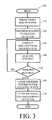
- FIG. 3illustrates a polishing procedure 300 utilized by polishing system 210 .
- the controller 280in step 310 of the polishing procedure 300 causes the polishing system 210 to begin polishing the front side of the semiconductor wafer 100 in order to remove material from the front side of the semiconductor wafer 100 .
- the controller 280causes the wafer carrier 232 to rub the front side of the semiconductor wafer 100 against the platen subassembly 220 .
- the controller 280causes the chemical slurry supply system 260 to apply chemical slurry atop platen subassembly in order to facilitate the removal of material from the front side of the semiconductor wafer 100 .
- the controller 280 in step 320causes the reagent supply system 240 to transfer reagent to the extraction conduit 272 of the endpoint detector 270 .
- the predetermined amount of polishing timeis close to but less than the amount of polishing time required for the polishing system 210 to reach the polishing endpoint layer 118 . Waiting until the polishing system 210 is closer to the polishing endpoint layer 118 before applying the reagent helps conserve the amount of reagent consumed by the polishing system 210 .
- the controller in step 330causes the extraction flow control 273 of the endpoint detector 270 to introduce effluent extracted from the platen subassembly 220 by the extraction conduit 272 into the testing area 274 .
- the endpoint detector 270analyzes in step 340 the effluent in order to determine whether the catalyst material of the polishing endpoint layer 118 has caused the reagent of the reagent supply system 240 to catalytically react.
- the reagentt-butyl bromide
- the sensor 276 of the preferred embodiment in step 350determines whether the reagent has caused the pH level of the effluent to drop below a predetermined level.
- the sensor 276may include a digital pH meter which detects the amount of hydrogen ions present in the effluent.
- the sensor 276may include an optical sensor which detects whether a pH indicator such as phenolphthalein has caused the effluent to change color. If sensor 276 determines that the reagent has catalytically reacted, then the sensor 276 transmits an endpoint signal to the controller 280 ; otherwise, the polishing system 210 returns to step 330 to extract more effluent.
- the controller 280 in step 360causes the polishing system 210 to stop polishing the semiconductor wafer 100 . It should be appreciated that the controller 280 may allow the polishing system 210 to continue polishing the semiconductor wafer 100 for a predetermined amount of time in order to further remove material from the semiconductor wafer 100 . This further removal of material or overpolishing may be desirable after certain steps of a fabrication process.
- the controller 280then in step 370 flushes the catalyst material from the polishing platen 220 and the endpoint detector 270 .
- the controller 280causes the chemical slurry to be applied to the polishing platen 220 for a predetermined period of time.
- the continual application of the chemical slurry after the polishing system 210 has stopped polishing the semiconductor wafer 100helps flush the catalyst material of the polishing endpoint layer 118 from the platen subassembly 220 and the endpoint detector 270 so that the endpoint detector 270 may detect the endpoint of the next semiconductor wafer to be polished.
- the catalytic reaction detected by the endpoint detector 270requires catalyst material and no other materials from the polishing endpoint layer 118 , a small amount of material removed from the polishing endpoint layer 118 can trigger a substantial catalytic reaction.
- This amplification effectenables the endpoint detector 270 to cost effectively detect presence of a small amount of polishing endpoint layer material by detecting a substantial catalytic reaction instead of trying to directly detect material removed from the polishing endpoint layer 118 .
- polishing endpoint layer 118has been described as being implanted into the semiconductor water 100 , other methods of forming the polishing endpoint layer 118 may also be used.
- U.S. Pat. No. 5, 668,063 to Fry et al.the disclosure which is hereby incorporated by reference, discloses forming a tracer layer upon other layers. This method of forming a tracer layer may be suitable for forming the catalytic polishing endpoint layer 118 used by the polishing system 210 of the present invention.
Landscapes
- Engineering & Computer Science (AREA)
- Mechanical Engineering (AREA)
- Physics & Mathematics (AREA)
- Condensed Matter Physics & Semiconductors (AREA)
- General Physics & Mathematics (AREA)
- Manufacturing & Machinery (AREA)
- Computer Hardware Design (AREA)
- Microelectronics & Electronic Packaging (AREA)
- Power Engineering (AREA)
- Finish Polishing, Edge Sharpening, And Grinding By Specific Grinding Devices (AREA)
- Mechanical Treatment Of Semiconductor (AREA)
Abstract
Description

Claims (8)
Priority Applications (1)
| Application Number | Priority Date | Filing Date | Title |
|---|---|---|---|
| US09/534,652US6258205B1 (en) | 1998-06-30 | 2000-03-24 | Endpoint detection method and apparatus which utilize an endpoint polishing layer of catalyst material |
Applications Claiming Priority (2)
| Application Number | Priority Date | Filing Date | Title |
|---|---|---|---|
| US09/109,331US6071818A (en) | 1998-06-30 | 1998-06-30 | Endpoint detection method and apparatus which utilize an endpoint polishing layer of catalyst material |
| US09/534,652US6258205B1 (en) | 1998-06-30 | 2000-03-24 | Endpoint detection method and apparatus which utilize an endpoint polishing layer of catalyst material |
Related Parent Applications (1)
| Application Number | Title | Priority Date | Filing Date |
|---|---|---|---|
| US09/109,331DivisionUS6071818A (en) | 1998-06-30 | 1998-06-30 | Endpoint detection method and apparatus which utilize an endpoint polishing layer of catalyst material |
Publications (1)
| Publication Number | Publication Date |
|---|---|
| US6258205B1true US6258205B1 (en) | 2001-07-10 |
Family
ID=22327094
Family Applications (2)
| Application Number | Title | Priority Date | Filing Date |
|---|---|---|---|
| US09/109,331Expired - LifetimeUS6071818A (en) | 1998-06-30 | 1998-06-30 | Endpoint detection method and apparatus which utilize an endpoint polishing layer of catalyst material |
| US09/534,652Expired - LifetimeUS6258205B1 (en) | 1998-06-30 | 2000-03-24 | Endpoint detection method and apparatus which utilize an endpoint polishing layer of catalyst material |
Family Applications Before (1)
| Application Number | Title | Priority Date | Filing Date |
|---|---|---|---|
| US09/109,331Expired - LifetimeUS6071818A (en) | 1998-06-30 | 1998-06-30 | Endpoint detection method and apparatus which utilize an endpoint polishing layer of catalyst material |
Country Status (1)
| Country | Link |
|---|---|
| US (2) | US6071818A (en) |
Cited By (10)
| Publication number | Priority date | Publication date | Assignee | Title |
|---|---|---|---|---|
| US6383332B1 (en)* | 1998-12-15 | 2002-05-07 | Lsi Logic Corporation | Endpoint detection method and apparatus which utilize a chelating agent to detect a polishing endpoint |
| US6579800B2 (en) | 2001-10-12 | 2003-06-17 | Nutool, Inc. | Chemical mechanical polishing endpoint detection |
| WO2003074228A1 (en)* | 2002-01-17 | 2003-09-12 | Nutool, Inc. | Advanced chemical mechanical polishing system with smart endpoint detection |
| EP1366860A1 (en)* | 2002-05-28 | 2003-12-03 | Asia Pacific Microsystem, Inc. | Non-destructive method for measuring the thickness of a bonded wafer |
| US20040060502A1 (en)* | 2002-09-26 | 2004-04-01 | University Of Florida | High selectivity and high planarity dielectric polishing |
| US6716364B1 (en)* | 1999-12-20 | 2004-04-06 | Lsi Logic Corporation | Method and apparatus for detecting presence of residual polishing slurry subsequent to polishing of a semiconductor wafer |
| US20040206374A1 (en)* | 2001-10-09 | 2004-10-21 | Dinesh Chopra | Inline monitoring of pad loading for CuCMP and developing an endpoint technique for cleaning |
| US6942546B2 (en) | 2002-01-17 | 2005-09-13 | Asm Nutool, Inc. | Endpoint detection for non-transparent polishing member |
| CN111627829A (en)* | 2019-02-27 | 2020-09-04 | 东芝存储器株式会社 | Substrate processing apparatus and manufacturing method of semiconductor device |
| US11171022B2 (en)* | 2018-08-27 | 2021-11-09 | Toshiba Memory Corporation | Substrate treatment apparatus and method of manufacturing semiconductor device |
Families Citing this family (14)
| Publication number | Priority date | Publication date | Assignee | Title |
|---|---|---|---|---|
| US6535779B1 (en)* | 1998-03-06 | 2003-03-18 | Applied Materials, Inc. | Apparatus and method for endpoint control and plasma monitoring |
| US6071818A (en)* | 1998-06-30 | 2000-06-06 | Lsi Logic Corporation | Endpoint detection method and apparatus which utilize an endpoint polishing layer of catalyst material |
| EP1125314A1 (en) | 1998-07-10 | 2001-08-22 | Applied Materials, Inc. | Improved endpoint detection for substrate fabrication processes |
| JP2001053039A (en)* | 1999-08-05 | 2001-02-23 | Okamoto Machine Tool Works Ltd | Wafer polishing end point detecting method and polishing end point detecting apparatus |
| US6291351B1 (en)* | 2000-06-28 | 2001-09-18 | International Business Machines Corporation | Endpoint detection in chemical-mechanical polishing of cloisonne structures |
| US6489242B1 (en) | 2000-09-13 | 2002-12-03 | Lsi Logic Corporation | Process for planarization of integrated circuit structure which inhibits cracking of low dielectric constant dielectric material adjacent underlying raised structures |
| US6319836B1 (en) | 2000-09-26 | 2001-11-20 | Lsi Logic Corporation | Planarization system |
| US6391768B1 (en) | 2000-10-30 | 2002-05-21 | Lsi Logic Corporation | Process for CMP removal of excess trench or via filler metal which inhibits formation of concave regions on oxide surface of integrated circuit structure |
| US6607967B1 (en) | 2000-11-15 | 2003-08-19 | Lsi Logic Corporation | Process for forming planarized isolation trench in integrated circuit structure on semiconductor substrate |
| US6439981B1 (en) | 2000-12-28 | 2002-08-27 | Lsi Logic Corporation | Arrangement and method for polishing a surface of a semiconductor wafer |
| US20030064521A1 (en)* | 2001-09-28 | 2003-04-03 | Zhijian Lu | Method for ending point detection during etching process |
| JP4041107B2 (en)* | 2004-09-22 | 2008-01-30 | 株式会社東芝 | Polishing method |
| TW200916261A (en)* | 2007-09-07 | 2009-04-16 | Cabot Microelectronics Corp | CMP sensor and control system |
| US9679782B1 (en)* | 2016-01-07 | 2017-06-13 | Taiwan Semiconductor Manufacturing Co., Ltd. | Planarization method, method for manufacturing semiconductor structure, and semiconductor structure |
Citations (98)
| Publication number | Priority date | Publication date | Assignee | Title |
|---|---|---|---|---|
| US3734620A (en) | 1971-04-01 | 1973-05-22 | Ibm | Multiple band atomic absorption apparatus for simultaneously measuring different physical parameters of a material |
| US3748014A (en) | 1971-12-22 | 1973-07-24 | Columbia Broadcasting Sys Inc | Near-confocal device for optical scan enhancement |
| US4312732A (en) | 1976-08-31 | 1982-01-26 | Bell Telephone Laboratories, Incorporated | Method for the optical monitoring of plasma discharge processing operations |
| US4374915A (en) | 1981-07-30 | 1983-02-22 | Intel Corporation | High contrast alignment marker for integrated circuit fabrication |
| US4632724A (en) | 1985-08-19 | 1986-12-30 | International Business Machines Corporation | Visibility enhancement of first order alignment marks |
| US4689491A (en) | 1985-04-19 | 1987-08-25 | Datasonics Corp. | Semiconductor wafer scanning system |
| US4793895A (en) | 1988-01-25 | 1988-12-27 | Ibm Corporation | In situ conductivity monitoring technique for chemical/mechanical planarization endpoint detection |
| US5036015A (en) | 1990-09-24 | 1991-07-30 | Micron Technology, Inc. | Method of endpoint detection during chemical/mechanical planarization of semiconductor wafers |
| US5081421A (en) | 1990-05-01 | 1992-01-14 | At&T Bell Laboratories | In situ monitoring technique and apparatus for chemical/mechanical planarization endpoint detection |
| US5151584A (en) | 1988-07-20 | 1992-09-29 | Applied Materials, Inc. | Method and apparatus for endpoint detection in a semiconductor wafer etching system |
| US5169491A (en) | 1991-07-29 | 1992-12-08 | Micron Technology, Inc. | Method of etching SiO2 dielectric layers using chemical mechanical polishing techniques |
| US5196353A (en) | 1992-01-03 | 1993-03-23 | Micron Technology, Inc. | Method for controlling a semiconductor (CMP) process by measuring a surface temperature and developing a thermal image of the wafer |
| US5222329A (en) | 1992-03-26 | 1993-06-29 | Micron Technology, Inc. | Acoustical method and system for detecting and controlling chemical-mechanical polishing (CMP) depths into layers of conductors, semiconductors, and dielectric materials |
| US5240552A (en) | 1991-12-11 | 1993-08-31 | Micron Technology, Inc. | Chemical mechanical planarization (CMP) of a semiconductor wafer using acoustical waves for in-situ end point detection |
| US5245790A (en) | 1992-02-14 | 1993-09-21 | Lsi Logic Corporation | Ultrasonic energy enhanced chemi-mechanical polishing of silicon wafers |
| US5245794A (en) | 1992-04-09 | 1993-09-21 | Advanced Micro Devices, Inc. | Audio end point detector for chemical-mechanical polishing and method therefor |
| US5258093A (en) | 1992-12-21 | 1993-11-02 | Motorola, Inc. | Procss for fabricating a ferroelectric capacitor in a semiconductor device |
| US5265378A (en) | 1992-07-10 | 1993-11-30 | Lsi Logic Corporation | Detecting the endpoint of chem-mech polishing and resulting semiconductor device |
| US5272115A (en) | 1991-01-09 | 1993-12-21 | Nec Corporation | Method of leveling the laminated surface of a semiconductor substrate |
| US5308438A (en) | 1992-01-30 | 1994-05-03 | International Business Machines Corporation | Endpoint detection apparatus and method for chemical/mechanical polishing |
| US5310455A (en) | 1992-07-10 | 1994-05-10 | Lsi Logic Corporation | Techniques for assembling polishing pads for chemi-mechanical polishing of silicon wafers |
| US5337015A (en) | 1993-06-14 | 1994-08-09 | International Business Machines Corporation | In-situ endpoint detection method and apparatus for chemical-mechanical polishing using low amplitude input voltage |
| US5362669A (en) | 1993-06-24 | 1994-11-08 | Northern Telecom Limited | Method of making integrated circuits |
| US5385866A (en) | 1994-06-22 | 1995-01-31 | International Business Machines Corporation | Polish planarizing using oxidized boron nitride as a polish stop |
| US5389194A (en) | 1993-02-05 | 1995-02-14 | Lsi Logic Corporation | Methods of cleaning semiconductor substrates after polishing |
| US5399234A (en) | 1993-09-29 | 1995-03-21 | Motorola Inc. | Acoustically regulated polishing process |
| US5403228A (en) | 1992-07-10 | 1995-04-04 | Lsi Logic Corporation | Techniques for assembling polishing pads for silicon wafer polishing |
| US5405806A (en) | 1994-03-29 | 1995-04-11 | Motorola Inc. | Method for forming a metal silicide interconnect in an integrated circuit |
| US5439551A (en) | 1994-03-02 | 1995-08-08 | Micron Technology, Inc. | Chemical-mechanical polishing techniques and methods of end point detection in chemical-mechanical polishing processes |
| US5449314A (en) | 1994-04-25 | 1995-09-12 | Micron Technology, Inc. | Method of chimical mechanical polishing for dielectric layers |
| US5483568A (en) | 1994-11-03 | 1996-01-09 | Kabushiki Kaisha Toshiba | Pad condition and polishing rate monitor using fluorescence |
| US5492594A (en) | 1994-09-26 | 1996-02-20 | International Business Machines Corp. | Chemical-mechanical polishing tool with end point measurement station |
| US5531861A (en) | 1993-09-29 | 1996-07-02 | Motorola, Inc. | Chemical-mechanical-polishing pad cleaning process for use during the fabrication of semiconductor devices |
| US5559428A (en) | 1995-04-10 | 1996-09-24 | International Business Machines Corporation | In-situ monitoring of the change in thickness of films |
| US5561541A (en) | 1984-09-05 | 1996-10-01 | The United States Of America As Represented By The Secretary Of The Army | Frustrated total internal reflection optical power limiter |
| US5595526A (en) | 1994-11-30 | 1997-01-21 | Intel Corporation | Method and apparatus for endpoint detection in a chemical/mechanical process for polishing a substrate |
| US5597442A (en) | 1995-10-16 | 1997-01-28 | Taiwan Semiconductor Manufacturing Company Ltd. | Chemical/mechanical planarization (CMP) endpoint method using measurement of polishing pad temperature |
| US5597590A (en) | 1990-02-20 | 1997-01-28 | Nikon Corporation | Apparatus for removing a thin film layer |
| US5607341A (en) | 1994-08-08 | 1997-03-04 | Leach; Michael A. | Method and structure for polishing a wafer during manufacture of integrated circuits |
| US5609511A (en) | 1994-04-14 | 1997-03-11 | Hitachi, Ltd. | Polishing method |
| US5614446A (en) | 1994-09-02 | 1997-03-25 | Advanced Micro Devices, Inc. | Holding apparatus, a metal deposition system, and a wafer processing method which preserve topographical marks on a semiconductor wafer |
| US5626715A (en) | 1993-02-05 | 1997-05-06 | Lsi Logic Corporation | Methods of polishing semiconductor substrates |
| US5627110A (en) | 1994-10-24 | 1997-05-06 | Advanced Micro Devices, Inc. | Method for eliminating window mask process in the fabrication of a semiconductor wafer when chemical-mechanical polish planarization is used |
| US5637185A (en) | 1995-03-30 | 1997-06-10 | Rensselaer Polytechnic Institute | Systems for performing chemical mechanical planarization and process for conducting same |
| US5639388A (en) | 1995-01-19 | 1997-06-17 | Ebara Corporation | Polishing endpoint detection method |
| US5643046A (en) | 1994-02-21 | 1997-07-01 | Kabushiki Kaisha Toshiba | Polishing method and apparatus for detecting a polishing end point of a semiconductor wafer |
| US5644221A (en) | 1996-03-19 | 1997-07-01 | International Business Machines Corporation | Endpoint detection for chemical mechanical polishing using frequency or amplitude mode |
| US5643050A (en) | 1996-05-23 | 1997-07-01 | Industrial Technology Research Institute | Chemical/mechanical polish (CMP) thickness monitor |
| US5643061A (en) | 1995-07-20 | 1997-07-01 | Integrated Process Equipment Corporation | Pneumatic polishing head for CMP apparatus |
| US5645682A (en) | 1996-05-28 | 1997-07-08 | Micron Technology, Inc. | Apparatus and method for conditioning a planarizing substrate used in chemical-mechanical planarization of semiconductor wafers |
| US5647952A (en) | 1996-04-01 | 1997-07-15 | Industrial Technology Research Institute | Chemical/mechanical polish (CMP) endpoint method |
| US5658183A (en) | 1993-08-25 | 1997-08-19 | Micron Technology, Inc. | System for real-time control of semiconductor wafer polishing including optical monitoring |
| US5660672A (en) | 1995-04-10 | 1997-08-26 | International Business Machines Corporation | In-situ monitoring of conductive films on semiconductor wafers |
| US5663101A (en) | 1995-09-07 | 1997-09-02 | International Business Machines Corporation | Semiconductor structure having multiple levels of self-aligned interconnection metallization, and methods for its preparation |
| US5663797A (en) | 1996-05-16 | 1997-09-02 | Micron Technology, Inc. | Method and apparatus for detecting the endpoint in chemical-mechanical polishing of semiconductor wafers |
| US5664987A (en) | 1994-01-31 | 1997-09-09 | National Semiconductor Corporation | Methods and apparatus for control of polishing pad conditioning for wafer planarization |
| US5668063A (en) | 1995-05-23 | 1997-09-16 | Watkins Johnson Company | Method of planarizing a layer of material |
| US5667629A (en) | 1996-06-21 | 1997-09-16 | Chartered Semiconductor Manufactuing Pte, Ltd. | Method and apparatus for determination of the end point in chemical mechanical polishing |
| US5667433A (en) | 1995-06-07 | 1997-09-16 | Lsi Logic Corporation | Keyed end effector for CMP pad conditioner |
| US5667424A (en) | 1996-09-25 | 1997-09-16 | Chartered Semiconductor Manufacturing Pte Ltd. | New chemical mechanical planarization (CMP) end point detection apparatus |
| US5670410A (en) | 1996-09-25 | 1997-09-23 | Chartered Semiconductor Manufacturing Pte Ltd. | Method of forming integrated CMP stopper and analog capacitor |
| US5672091A (en) | 1994-12-22 | 1997-09-30 | Ebara Corporation | Polishing apparatus having endpoint detection device |
| US5674784A (en) | 1996-10-02 | 1997-10-07 | Taiwan Semiconductor Manufacturing Company, Ltd. | Method for forming polish stop layer for CMP process |
| US5681215A (en) | 1995-10-27 | 1997-10-28 | Applied Materials, Inc. | Carrier head design for a chemical mechanical polishing apparatus |
| US5691253A (en) | 1994-06-02 | 1997-11-25 | Motorola, Inc. | Process for polishing and analyzing an exposed surface of a patterned semiconductor |
| US5695660A (en) | 1992-09-17 | 1997-12-09 | Luxtron Corporation | Optical techniques of measuring endpoint during the processing of material layers in an optically hostile environment |
| US5700180A (en) | 1993-08-25 | 1997-12-23 | Micron Technology, Inc. | System for real-time control of semiconductor wafer polishing |
| US5702292A (en) | 1996-10-31 | 1997-12-30 | Micron Technology, Inc. | Apparatus and method for loading and unloading substrates to a chemical-mechanical planarization machine |
| US5705435A (en) | 1996-08-09 | 1998-01-06 | Industrial Technology Research Institute | Chemical-mechanical polishing (CMP) apparatus |
| US5704987A (en) | 1996-01-19 | 1998-01-06 | International Business Machines Corporation | Process for removing residue from a semiconductor wafer after chemical-mechanical polishing |
| US5705320A (en) | 1996-11-12 | 1998-01-06 | Taiwan Semiconductor Manufacturing Company, Ltd. | Recovery of alignment marks and laser marks after chemical-mechanical-polishing |
| US5710076A (en) | 1996-09-03 | 1998-01-20 | Industrial Technology Research Institute | Method for fabricating a sub-half micron MOSFET device with global planarization of insulator filled shallow trenches, via the use of a bottom anti-reflective coating |
| US5712185A (en) | 1996-04-23 | 1998-01-27 | United Microelectronics | Method for forming shallow trench isolation |
| US5716873A (en) | 1996-05-06 | 1998-02-10 | Micro Technology, Inc. | Method for cleaning waste matter from the backside of a semiconductor wafer substrate |
| US5720845A (en) | 1996-01-17 | 1998-02-24 | Liu; Keh-Shium | Wafer polisher head used for chemical-mechanical polishing and endpoint detection |
| US5722875A (en) | 1995-05-30 | 1998-03-03 | Tokyo Electron Limited | Method and apparatus for polishing |
| US5722877A (en) | 1996-10-11 | 1998-03-03 | Lam Research Corporation | Technique for improving within-wafer non-uniformity of material removal for performing CMP |
| US5725417A (en) | 1996-11-05 | 1998-03-10 | Micron Technology, Inc. | Method and apparatus for conditioning polishing pads used in mechanical and chemical-mechanical planarization of substrates |
| US5736462A (en) | 1995-05-15 | 1998-04-07 | Sony Corporation | Method of etching back layer on substrate |
| US5738567A (en) | 1996-08-20 | 1998-04-14 | Micron Technology, Inc. | Polishing pad for chemical-mechanical planarization of a semiconductor wafer |
| US5741171A (en) | 1996-08-19 | 1998-04-21 | Sagitta Engineering Solutions, Ltd. | Precision polishing system |
| US5747380A (en) | 1996-02-26 | 1998-05-05 | Taiwan Semiconductor Manufacturing Company, Ltd. | Robust end-point detection for contact and via etching |
| US5755614A (en) | 1996-07-29 | 1998-05-26 | Integrated Process Equipment Corporation | Rinse water recycling in CMP apparatus |
| US5762536A (en) | 1996-04-26 | 1998-06-09 | Lam Research Corporation | Sensors for a linear polisher |
| US5777739A (en) | 1996-02-16 | 1998-07-07 | Micron Technology, Inc. | Endpoint detector and method for measuring a change in wafer thickness in chemical-mechanical polishing of semiconductor wafers |
| US5795495A (en) | 1994-04-25 | 1998-08-18 | Micron Technology, Inc. | Method of chemical mechanical polishing for dielectric layers |
| US5861055A (en) | 1995-12-29 | 1999-01-19 | Lsi Logic Corporation | Polishing composition for CMP operations |
| US5865666A (en) | 1997-08-20 | 1999-02-02 | Lsi Logic Corporation | Apparatus and method for polish removing a precise amount of material from a wafer |
| US5868608A (en) | 1996-08-13 | 1999-02-09 | Lsi Logic Corporation | Subsonic to supersonic and ultrasonic conditioning of a polishing pad in a chemical mechanical polishing apparatus |
| US5882251A (en) | 1997-08-19 | 1999-03-16 | Lsi Logic Corporation | Chemical mechanical polishing pad slurry distribution grooves |
| US5882244A (en) | 1995-07-20 | 1999-03-16 | Ebara Corporation | Polishing apparatus |
| US5888120A (en) | 1997-09-29 | 1999-03-30 | Lsi Logic Corporation | Method and apparatus for chemical mechanical polishing |
| US5893756A (en) | 1997-08-26 | 1999-04-13 | Lsi Logic Corporation | Use of ethylene glycol as a corrosion inhibitor during cleaning after metal chemical mechanical polishing |
| US5931719A (en) | 1997-08-25 | 1999-08-03 | Lsi Logic Corporation | Method and apparatus for using pressure differentials through a polishing pad to improve performance in chemical mechanical polishing |
| US5948697A (en) | 1996-05-23 | 1999-09-07 | Lsi Logic Corporation | Catalytic acceleration and electrical bias control of CMP processing |
| US5957757A (en) | 1997-10-30 | 1999-09-28 | Lsi Logic Corporation | Conditioning CMP polishing pad using a high pressure fluid |
| US6071818A (en)* | 1998-06-30 | 2000-06-06 | Lsi Logic Corporation | Endpoint detection method and apparatus which utilize an endpoint polishing layer of catalyst material |
| US6126848A (en)* | 1998-05-06 | 2000-10-03 | International Business Machines Corporation | Indirect endpoint detection by chemical reaction and chemiluminescence |
- 1998
- 1998-06-30USUS09/109,331patent/US6071818A/ennot_activeExpired - Lifetime
- 2000
- 2000-03-24USUS09/534,652patent/US6258205B1/ennot_activeExpired - Lifetime
Patent Citations (103)
| Publication number | Priority date | Publication date | Assignee | Title |
|---|---|---|---|---|
| US3734620A (en) | 1971-04-01 | 1973-05-22 | Ibm | Multiple band atomic absorption apparatus for simultaneously measuring different physical parameters of a material |
| US3748014A (en) | 1971-12-22 | 1973-07-24 | Columbia Broadcasting Sys Inc | Near-confocal device for optical scan enhancement |
| US4312732A (en) | 1976-08-31 | 1982-01-26 | Bell Telephone Laboratories, Incorporated | Method for the optical monitoring of plasma discharge processing operations |
| US4374915A (en) | 1981-07-30 | 1983-02-22 | Intel Corporation | High contrast alignment marker for integrated circuit fabrication |
| US5561541A (en) | 1984-09-05 | 1996-10-01 | The United States Of America As Represented By The Secretary Of The Army | Frustrated total internal reflection optical power limiter |
| US4689491A (en) | 1985-04-19 | 1987-08-25 | Datasonics Corp. | Semiconductor wafer scanning system |
| US4632724A (en) | 1985-08-19 | 1986-12-30 | International Business Machines Corporation | Visibility enhancement of first order alignment marks |
| US4793895A (en) | 1988-01-25 | 1988-12-27 | Ibm Corporation | In situ conductivity monitoring technique for chemical/mechanical planarization endpoint detection |
| US5151584A (en) | 1988-07-20 | 1992-09-29 | Applied Materials, Inc. | Method and apparatus for endpoint detection in a semiconductor wafer etching system |
| US5656229A (en) | 1990-02-20 | 1997-08-12 | Nikon Corporation | Method for removing a thin film layer |
| US5597590A (en) | 1990-02-20 | 1997-01-28 | Nikon Corporation | Apparatus for removing a thin film layer |
| US5081421A (en) | 1990-05-01 | 1992-01-14 | At&T Bell Laboratories | In situ monitoring technique and apparatus for chemical/mechanical planarization endpoint detection |
| US5036015A (en) | 1990-09-24 | 1991-07-30 | Micron Technology, Inc. | Method of endpoint detection during chemical/mechanical planarization of semiconductor wafers |
| US5272115A (en) | 1991-01-09 | 1993-12-21 | Nec Corporation | Method of leveling the laminated surface of a semiconductor substrate |
| US5169491A (en) | 1991-07-29 | 1992-12-08 | Micron Technology, Inc. | Method of etching SiO2 dielectric layers using chemical mechanical polishing techniques |
| US5240552A (en) | 1991-12-11 | 1993-08-31 | Micron Technology, Inc. | Chemical mechanical planarization (CMP) of a semiconductor wafer using acoustical waves for in-situ end point detection |
| US5196353A (en) | 1992-01-03 | 1993-03-23 | Micron Technology, Inc. | Method for controlling a semiconductor (CMP) process by measuring a surface temperature and developing a thermal image of the wafer |
| US5308438A (en) | 1992-01-30 | 1994-05-03 | International Business Machines Corporation | Endpoint detection apparatus and method for chemical/mechanical polishing |
| US5245790A (en) | 1992-02-14 | 1993-09-21 | Lsi Logic Corporation | Ultrasonic energy enhanced chemi-mechanical polishing of silicon wafers |
| US5222329A (en) | 1992-03-26 | 1993-06-29 | Micron Technology, Inc. | Acoustical method and system for detecting and controlling chemical-mechanical polishing (CMP) depths into layers of conductors, semiconductors, and dielectric materials |
| US5245794A (en) | 1992-04-09 | 1993-09-21 | Advanced Micro Devices, Inc. | Audio end point detector for chemical-mechanical polishing and method therefor |
| US5310455A (en) | 1992-07-10 | 1994-05-10 | Lsi Logic Corporation | Techniques for assembling polishing pads for chemi-mechanical polishing of silicon wafers |
| US5321304A (en) | 1992-07-10 | 1994-06-14 | Lsi Logic Corporation | Detecting the endpoint of chem-mech polishing, and resulting semiconductor device |
| US5624304A (en) | 1992-07-10 | 1997-04-29 | Lsi Logic, Inc. | Techniques for assembling polishing pads for chemi-mechanical polishing of silicon wafers |
| US5516400A (en) | 1992-07-10 | 1996-05-14 | Lsi Logic Corporation | Techniques for assembling polishing pads for chemical-mechanical polishing of silicon wafers |
| US5403228A (en) | 1992-07-10 | 1995-04-04 | Lsi Logic Corporation | Techniques for assembling polishing pads for silicon wafer polishing |
| US5265378A (en) | 1992-07-10 | 1993-11-30 | Lsi Logic Corporation | Detecting the endpoint of chem-mech polishing and resulting semiconductor device |
| US5695660A (en) | 1992-09-17 | 1997-12-09 | Luxtron Corporation | Optical techniques of measuring endpoint during the processing of material layers in an optically hostile environment |
| US5258093A (en) | 1992-12-21 | 1993-11-02 | Motorola, Inc. | Procss for fabricating a ferroelectric capacitor in a semiconductor device |
| US5389194A (en) | 1993-02-05 | 1995-02-14 | Lsi Logic Corporation | Methods of cleaning semiconductor substrates after polishing |
| US5626715A (en) | 1993-02-05 | 1997-05-06 | Lsi Logic Corporation | Methods of polishing semiconductor substrates |
| US5337015A (en) | 1993-06-14 | 1994-08-09 | International Business Machines Corporation | In-situ endpoint detection method and apparatus for chemical-mechanical polishing using low amplitude input voltage |
| US5362669A (en) | 1993-06-24 | 1994-11-08 | Northern Telecom Limited | Method of making integrated circuits |
| US5658183A (en) | 1993-08-25 | 1997-08-19 | Micron Technology, Inc. | System for real-time control of semiconductor wafer polishing including optical monitoring |
| US5700180A (en) | 1993-08-25 | 1997-12-23 | Micron Technology, Inc. | System for real-time control of semiconductor wafer polishing |
| US5762537A (en) | 1993-08-25 | 1998-06-09 | Micron Technology, Inc. | System for real-time control of semiconductor wafer polishing including heater |
| US5531861A (en) | 1993-09-29 | 1996-07-02 | Motorola, Inc. | Chemical-mechanical-polishing pad cleaning process for use during the fabrication of semiconductor devices |
| US5399234A (en) | 1993-09-29 | 1995-03-21 | Motorola Inc. | Acoustically regulated polishing process |
| US5664987A (en) | 1994-01-31 | 1997-09-09 | National Semiconductor Corporation | Methods and apparatus for control of polishing pad conditioning for wafer planarization |
| US5643046A (en) | 1994-02-21 | 1997-07-01 | Kabushiki Kaisha Toshiba | Polishing method and apparatus for detecting a polishing end point of a semiconductor wafer |
| US5439551A (en) | 1994-03-02 | 1995-08-08 | Micron Technology, Inc. | Chemical-mechanical polishing techniques and methods of end point detection in chemical-mechanical polishing processes |
| US5405806A (en) | 1994-03-29 | 1995-04-11 | Motorola Inc. | Method for forming a metal silicide interconnect in an integrated circuit |
| US5609511A (en) | 1994-04-14 | 1997-03-11 | Hitachi, Ltd. | Polishing method |
| US5449314A (en) | 1994-04-25 | 1995-09-12 | Micron Technology, Inc. | Method of chimical mechanical polishing for dielectric layers |
| US5795495A (en) | 1994-04-25 | 1998-08-18 | Micron Technology, Inc. | Method of chemical mechanical polishing for dielectric layers |
| US5691253A (en) | 1994-06-02 | 1997-11-25 | Motorola, Inc. | Process for polishing and analyzing an exposed surface of a patterned semiconductor |
| US5385866A (en) | 1994-06-22 | 1995-01-31 | International Business Machines Corporation | Polish planarizing using oxidized boron nitride as a polish stop |
| US5607341A (en) | 1994-08-08 | 1997-03-04 | Leach; Michael A. | Method and structure for polishing a wafer during manufacture of integrated circuits |
| US5614446A (en) | 1994-09-02 | 1997-03-25 | Advanced Micro Devices, Inc. | Holding apparatus, a metal deposition system, and a wafer processing method which preserve topographical marks on a semiconductor wafer |
| US5492594A (en) | 1994-09-26 | 1996-02-20 | International Business Machines Corp. | Chemical-mechanical polishing tool with end point measurement station |
| US5627110A (en) | 1994-10-24 | 1997-05-06 | Advanced Micro Devices, Inc. | Method for eliminating window mask process in the fabrication of a semiconductor wafer when chemical-mechanical polish planarization is used |
| US5483568A (en) | 1994-11-03 | 1996-01-09 | Kabushiki Kaisha Toshiba | Pad condition and polishing rate monitor using fluorescence |
| US5595526A (en) | 1994-11-30 | 1997-01-21 | Intel Corporation | Method and apparatus for endpoint detection in a chemical/mechanical process for polishing a substrate |
| US5672091A (en) | 1994-12-22 | 1997-09-30 | Ebara Corporation | Polishing apparatus having endpoint detection device |
| US5639388A (en) | 1995-01-19 | 1997-06-17 | Ebara Corporation | Polishing endpoint detection method |
| US5637185A (en) | 1995-03-30 | 1997-06-10 | Rensselaer Polytechnic Institute | Systems for performing chemical mechanical planarization and process for conducting same |
| US5559428A (en) | 1995-04-10 | 1996-09-24 | International Business Machines Corporation | In-situ monitoring of the change in thickness of films |
| US5660672A (en) | 1995-04-10 | 1997-08-26 | International Business Machines Corporation | In-situ monitoring of conductive films on semiconductor wafers |
| US5736462A (en) | 1995-05-15 | 1998-04-07 | Sony Corporation | Method of etching back layer on substrate |
| US5668063A (en) | 1995-05-23 | 1997-09-16 | Watkins Johnson Company | Method of planarizing a layer of material |
| US5722875A (en) | 1995-05-30 | 1998-03-03 | Tokyo Electron Limited | Method and apparatus for polishing |
| US5667433A (en) | 1995-06-07 | 1997-09-16 | Lsi Logic Corporation | Keyed end effector for CMP pad conditioner |
| US5643061A (en) | 1995-07-20 | 1997-07-01 | Integrated Process Equipment Corporation | Pneumatic polishing head for CMP apparatus |
| US5882244A (en) | 1995-07-20 | 1999-03-16 | Ebara Corporation | Polishing apparatus |
| US5663101A (en) | 1995-09-07 | 1997-09-02 | International Business Machines Corporation | Semiconductor structure having multiple levels of self-aligned interconnection metallization, and methods for its preparation |
| US5597442A (en) | 1995-10-16 | 1997-01-28 | Taiwan Semiconductor Manufacturing Company Ltd. | Chemical/mechanical planarization (CMP) endpoint method using measurement of polishing pad temperature |
| US5681215A (en) | 1995-10-27 | 1997-10-28 | Applied Materials, Inc. | Carrier head design for a chemical mechanical polishing apparatus |
| US5861055A (en) | 1995-12-29 | 1999-01-19 | Lsi Logic Corporation | Polishing composition for CMP operations |
| US5720845A (en) | 1996-01-17 | 1998-02-24 | Liu; Keh-Shium | Wafer polisher head used for chemical-mechanical polishing and endpoint detection |
| US5704987A (en) | 1996-01-19 | 1998-01-06 | International Business Machines Corporation | Process for removing residue from a semiconductor wafer after chemical-mechanical polishing |
| US5777739A (en) | 1996-02-16 | 1998-07-07 | Micron Technology, Inc. | Endpoint detector and method for measuring a change in wafer thickness in chemical-mechanical polishing of semiconductor wafers |
| US5747380A (en) | 1996-02-26 | 1998-05-05 | Taiwan Semiconductor Manufacturing Company, Ltd. | Robust end-point detection for contact and via etching |
| US5644221A (en) | 1996-03-19 | 1997-07-01 | International Business Machines Corporation | Endpoint detection for chemical mechanical polishing using frequency or amplitude mode |
| US5647952A (en) | 1996-04-01 | 1997-07-15 | Industrial Technology Research Institute | Chemical/mechanical polish (CMP) endpoint method |
| US5712185A (en) | 1996-04-23 | 1998-01-27 | United Microelectronics | Method for forming shallow trench isolation |
| US5762536A (en) | 1996-04-26 | 1998-06-09 | Lam Research Corporation | Sensors for a linear polisher |
| US5716873A (en) | 1996-05-06 | 1998-02-10 | Micro Technology, Inc. | Method for cleaning waste matter from the backside of a semiconductor wafer substrate |
| US5663797A (en) | 1996-05-16 | 1997-09-02 | Micron Technology, Inc. | Method and apparatus for detecting the endpoint in chemical-mechanical polishing of semiconductor wafers |
| US5948697A (en) | 1996-05-23 | 1999-09-07 | Lsi Logic Corporation | Catalytic acceleration and electrical bias control of CMP processing |
| US5643050A (en) | 1996-05-23 | 1997-07-01 | Industrial Technology Research Institute | Chemical/mechanical polish (CMP) thickness monitor |
| US5645682A (en) | 1996-05-28 | 1997-07-08 | Micron Technology, Inc. | Apparatus and method for conditioning a planarizing substrate used in chemical-mechanical planarization of semiconductor wafers |
| US5667629A (en) | 1996-06-21 | 1997-09-16 | Chartered Semiconductor Manufactuing Pte, Ltd. | Method and apparatus for determination of the end point in chemical mechanical polishing |
| US5755614A (en) | 1996-07-29 | 1998-05-26 | Integrated Process Equipment Corporation | Rinse water recycling in CMP apparatus |
| US5705435A (en) | 1996-08-09 | 1998-01-06 | Industrial Technology Research Institute | Chemical-mechanical polishing (CMP) apparatus |
| US5868608A (en) | 1996-08-13 | 1999-02-09 | Lsi Logic Corporation | Subsonic to supersonic and ultrasonic conditioning of a polishing pad in a chemical mechanical polishing apparatus |
| US5741171A (en) | 1996-08-19 | 1998-04-21 | Sagitta Engineering Solutions, Ltd. | Precision polishing system |
| US5738567A (en) | 1996-08-20 | 1998-04-14 | Micron Technology, Inc. | Polishing pad for chemical-mechanical planarization of a semiconductor wafer |
| US5710076A (en) | 1996-09-03 | 1998-01-20 | Industrial Technology Research Institute | Method for fabricating a sub-half micron MOSFET device with global planarization of insulator filled shallow trenches, via the use of a bottom anti-reflective coating |
| US5667424A (en) | 1996-09-25 | 1997-09-16 | Chartered Semiconductor Manufacturing Pte Ltd. | New chemical mechanical planarization (CMP) end point detection apparatus |
| US5670410A (en) | 1996-09-25 | 1997-09-23 | Chartered Semiconductor Manufacturing Pte Ltd. | Method of forming integrated CMP stopper and analog capacitor |
| US5674784A (en) | 1996-10-02 | 1997-10-07 | Taiwan Semiconductor Manufacturing Company, Ltd. | Method for forming polish stop layer for CMP process |
| US5722877A (en) | 1996-10-11 | 1998-03-03 | Lam Research Corporation | Technique for improving within-wafer non-uniformity of material removal for performing CMP |
| US5702292A (en) | 1996-10-31 | 1997-12-30 | Micron Technology, Inc. | Apparatus and method for loading and unloading substrates to a chemical-mechanical planarization machine |
| US5725417A (en) | 1996-11-05 | 1998-03-10 | Micron Technology, Inc. | Method and apparatus for conditioning polishing pads used in mechanical and chemical-mechanical planarization of substrates |
| US5705320A (en) | 1996-11-12 | 1998-01-06 | Taiwan Semiconductor Manufacturing Company, Ltd. | Recovery of alignment marks and laser marks after chemical-mechanical-polishing |
| US5882251A (en) | 1997-08-19 | 1999-03-16 | Lsi Logic Corporation | Chemical mechanical polishing pad slurry distribution grooves |
| US5865666A (en) | 1997-08-20 | 1999-02-02 | Lsi Logic Corporation | Apparatus and method for polish removing a precise amount of material from a wafer |
| US5931719A (en) | 1997-08-25 | 1999-08-03 | Lsi Logic Corporation | Method and apparatus for using pressure differentials through a polishing pad to improve performance in chemical mechanical polishing |
| US5893756A (en) | 1997-08-26 | 1999-04-13 | Lsi Logic Corporation | Use of ethylene glycol as a corrosion inhibitor during cleaning after metal chemical mechanical polishing |
| US5888120A (en) | 1997-09-29 | 1999-03-30 | Lsi Logic Corporation | Method and apparatus for chemical mechanical polishing |
| US5957757A (en) | 1997-10-30 | 1999-09-28 | Lsi Logic Corporation | Conditioning CMP polishing pad using a high pressure fluid |
| US6126848A (en)* | 1998-05-06 | 2000-10-03 | International Business Machines Corporation | Indirect endpoint detection by chemical reaction and chemiluminescence |
| US6071818A (en)* | 1998-06-30 | 2000-06-06 | Lsi Logic Corporation | Endpoint detection method and apparatus which utilize an endpoint polishing layer of catalyst material |
Cited By (16)
| Publication number | Priority date | Publication date | Assignee | Title |
|---|---|---|---|---|
| US6383332B1 (en)* | 1998-12-15 | 2002-05-07 | Lsi Logic Corporation | Endpoint detection method and apparatus which utilize a chelating agent to detect a polishing endpoint |
| US6716364B1 (en)* | 1999-12-20 | 2004-04-06 | Lsi Logic Corporation | Method and apparatus for detecting presence of residual polishing slurry subsequent to polishing of a semiconductor wafer |
| US20040206374A1 (en)* | 2001-10-09 | 2004-10-21 | Dinesh Chopra | Inline monitoring of pad loading for CuCMP and developing an endpoint technique for cleaning |
| US8557132B2 (en)* | 2001-10-09 | 2013-10-15 | Micron Technology, Inc. | Inline monitoring of pad loading for CuCMP and developing an endpoint technique for cleaning |
| US6579800B2 (en) | 2001-10-12 | 2003-06-17 | Nutool, Inc. | Chemical mechanical polishing endpoint detection |
| US20030213558A1 (en)* | 2001-10-12 | 2003-11-20 | Bulent Basol | Chemical mechanical polishing endpoint detection |
| WO2003074228A1 (en)* | 2002-01-17 | 2003-09-12 | Nutool, Inc. | Advanced chemical mechanical polishing system with smart endpoint detection |
| US6942546B2 (en) | 2002-01-17 | 2005-09-13 | Asm Nutool, Inc. | Endpoint detection for non-transparent polishing member |
| EP1366860A1 (en)* | 2002-05-28 | 2003-12-03 | Asia Pacific Microsystem, Inc. | Non-destructive method for measuring the thickness of a bonded wafer |
| US6866793B2 (en) | 2002-09-26 | 2005-03-15 | University Of Florida Research Foundation, Inc. | High selectivity and high planarity dielectric polishing |
| WO2004030041A3 (en)* | 2002-09-26 | 2004-07-01 | Univ Florida | High selectivity and high planarity dielectric polishing |
| US20040060502A1 (en)* | 2002-09-26 | 2004-04-01 | University Of Florida | High selectivity and high planarity dielectric polishing |
| US11171022B2 (en)* | 2018-08-27 | 2021-11-09 | Toshiba Memory Corporation | Substrate treatment apparatus and method of manufacturing semiconductor device |
| CN111627829A (en)* | 2019-02-27 | 2020-09-04 | 东芝存储器株式会社 | Substrate processing apparatus and manufacturing method of semiconductor device |
| US11171020B2 (en)* | 2019-02-27 | 2021-11-09 | Toshiba Memory Corporation | Substrate treatment apparatus |
| CN111627829B (en)* | 2019-02-27 | 2024-04-09 | 铠侠股份有限公司 | Substrate processing device and method for manufacturing semiconductor device |
Also Published As
| Publication number | Publication date |
|---|---|
| US6071818A (en) | 2000-06-06 |
Similar Documents
| Publication | Publication Date | Title |
|---|---|---|
| US6258205B1 (en) | Endpoint detection method and apparatus which utilize an endpoint polishing layer of catalyst material | |
| US6383332B1 (en) | Endpoint detection method and apparatus which utilize a chelating agent to detect a polishing endpoint | |
| US7132035B2 (en) | Methods, apparatuses, and substrate assembly structures for fabricating microelectronic components using mechanical and chemical-mechanical planarization processes | |
| US6007408A (en) | Method and apparatus for endpointing mechanical and chemical-mechanical polishing of substrates | |
| US6238273B1 (en) | Methods for predicting polishing parameters of polishing pads and methods and machines for planarizing microelectronic substrate assemblies in mechanical or chemical-mechanical planarization | |
| KR20010078154A (en) | Endpoint monitoring with polishing rate change | |
| TW200403129A (en) | Polishing pad for endpoint detection and related methods | |
| US6121147A (en) | Apparatus and method of detecting a polishing endpoint layer of a semiconductor wafer which includes a metallic reporting substance | |
| CN101484979A (en) | Method and apparatus for chemical mechanical polishing of large size wafer with capability of polishing individual die | |
| US6716364B1 (en) | Method and apparatus for detecting presence of residual polishing slurry subsequent to polishing of a semiconductor wafer | |
| US20060113036A1 (en) | Computer integrated manufacturing control system for oxide chemical mechanical polishing | |
| US6080670A (en) | Method of detecting a polishing endpoint layer of a semiconductor wafer which includes a non-reactive reporting specie | |
| US6074517A (en) | Method and apparatus for detecting an endpoint polishing layer by transmitting infrared light signals through a semiconductor wafer | |
| US6354908B2 (en) | Method and apparatus for detecting a planarized outer layer of a semiconductor wafer with a confocal optical system | |
| US5972787A (en) | CMP process using indicator areas to determine endpoint | |
| US6316276B1 (en) | Apparatus and method of planarizing a semiconductor wafer that includes a first reflective substance and a second reflective substance | |
| KR100669644B1 (en) | Chemical mechanical polishing apparatus and method | |
| US6884144B2 (en) | Methods and systems for planarizing microelectronic devices with Ge-Se-Ag layers | |
| US6268224B1 (en) | Method and apparatus for detecting an ion-implanted polishing endpoint layer within a semiconductor wafer | |
| JPH09131660A (en) | Semiconductor manufacturing apparatus and method | |
| US6285035B1 (en) | Apparatus for detecting an endpoint polishing layer of a semiconductor wafer having a wafer carrier with independent concentric sub-carriers and associated method | |
| US6478659B2 (en) | Chemical mechanical polishing method for slurry free fixed abrasive pads | |
| US6872662B1 (en) | Method for detecting the endpoint of a chemical mechanical polishing (CMP) process | |
| JP2001088008A (en) | Polishing method and apparatus | |
| EP1618991B1 (en) | Polishing pad |
Legal Events
| Date | Code | Title | Description |
|---|---|---|---|
| AS | Assignment | Owner name:LSI LOGIC CORPORATION, CALIFORNIA Free format text:ASSIGNMENT OF ASSIGNORS INTEREST;ASSIGNORS:CHISHOLM, BRYNNE;SHELTON, GAIL;MILLER, GAYLE;REEL/FRAME:010870/0001;SIGNING DATES FROM 19980807 TO 19980812 | |
| STCF | Information on status: patent grant | Free format text:PATENTED CASE | |
| FPAY | Fee payment | Year of fee payment:4 | |
| FEPP | Fee payment procedure | Free format text:PAYOR NUMBER ASSIGNED (ORIGINAL EVENT CODE: ASPN); ENTITY STATUS OF PATENT OWNER: LARGE ENTITY Free format text:PAYER NUMBER DE-ASSIGNED (ORIGINAL EVENT CODE: RMPN); ENTITY STATUS OF PATENT OWNER: LARGE ENTITY | |
| FPAY | Fee payment | Year of fee payment:8 | |
| FPAY | Fee payment | Year of fee payment:12 | |
| AS | Assignment | Owner name:DEUTSCHE BANK AG NEW YORK BRANCH, AS COLLATERAL AG Free format text:PATENT SECURITY AGREEMENT;ASSIGNORS:LSI CORPORATION;AGERE SYSTEMS LLC;REEL/FRAME:032856/0031 Effective date:20140506 | |
| AS | Assignment | Owner name:LSI CORPORATION, CALIFORNIA Free format text:CHANGE OF NAME;ASSIGNOR:LSI LOGIC CORPORATION;REEL/FRAME:033102/0270 Effective date:20070406 | |
| AS | Assignment | Owner name:AVAGO TECHNOLOGIES GENERAL IP (SINGAPORE) PTE. LTD Free format text:ASSIGNMENT OF ASSIGNORS INTEREST;ASSIGNOR:LSI CORPORATION;REEL/FRAME:035390/0388 Effective date:20140814 | |
| AS | Assignment | Owner name:LSI CORPORATION, CALIFORNIA Free format text:TERMINATION AND RELEASE OF SECURITY INTEREST IN PATENT RIGHTS (RELEASES RF 032856-0031);ASSIGNOR:DEUTSCHE BANK AG NEW YORK BRANCH, AS COLLATERAL AGENT;REEL/FRAME:037684/0039 Effective date:20160201 Owner name:AGERE SYSTEMS LLC, PENNSYLVANIA Free format text:TERMINATION AND RELEASE OF SECURITY INTEREST IN PATENT RIGHTS (RELEASES RF 032856-0031);ASSIGNOR:DEUTSCHE BANK AG NEW YORK BRANCH, AS COLLATERAL AGENT;REEL/FRAME:037684/0039 Effective date:20160201 | |
| AS | Assignment | Owner name:BANK OF AMERICA, N.A., AS COLLATERAL AGENT, NORTH CAROLINA Free format text:PATENT SECURITY AGREEMENT;ASSIGNOR:AVAGO TECHNOLOGIES GENERAL IP (SINGAPORE) PTE. LTD.;REEL/FRAME:037808/0001 Effective date:20160201 Owner name:BANK OF AMERICA, N.A., AS COLLATERAL AGENT, NORTH Free format text:PATENT SECURITY AGREEMENT;ASSIGNOR:AVAGO TECHNOLOGIES GENERAL IP (SINGAPORE) PTE. LTD.;REEL/FRAME:037808/0001 Effective date:20160201 | |
| AS | Assignment | Owner name:AVAGO TECHNOLOGIES GENERAL IP (SINGAPORE) PTE. LTD., SINGAPORE Free format text:TERMINATION AND RELEASE OF SECURITY INTEREST IN PATENTS;ASSIGNOR:BANK OF AMERICA, N.A., AS COLLATERAL AGENT;REEL/FRAME:041710/0001 Effective date:20170119 Owner name:AVAGO TECHNOLOGIES GENERAL IP (SINGAPORE) PTE. LTD Free format text:TERMINATION AND RELEASE OF SECURITY INTEREST IN PATENTS;ASSIGNOR:BANK OF AMERICA, N.A., AS COLLATERAL AGENT;REEL/FRAME:041710/0001 Effective date:20170119 | |
| AS | Assignment | Owner name:BELL SEMICONDUCTOR, LLC, ILLINOIS Free format text:ASSIGNMENT OF ASSIGNORS INTEREST;ASSIGNORS:AVAGO TECHNOLOGIES GENERAL IP (SINGAPORE) PTE. LTD.;BROADCOM CORPORATION;REEL/FRAME:044886/0001 Effective date:20171208 | |
| AS | Assignment | Owner name:CORTLAND CAPITAL MARKET SERVICES LLC, AS COLLATERA Free format text:SECURITY INTEREST;ASSIGNORS:HILCO PATENT ACQUISITION 56, LLC;BELL SEMICONDUCTOR, LLC;BELL NORTHERN RESEARCH, LLC;REEL/FRAME:045216/0020 Effective date:20180124 | |
| AS | Assignment | Owner name:BELL NORTHERN RESEARCH, LLC, ILLINOIS Free format text:SECURITY INTEREST;ASSIGNOR:CORTLAND CAPITAL MARKET SERVICES LLC;REEL/FRAME:060885/0001 Effective date:20220401 Owner name:BELL SEMICONDUCTOR, LLC, ILLINOIS Free format text:SECURITY INTEREST;ASSIGNOR:CORTLAND CAPITAL MARKET SERVICES LLC;REEL/FRAME:060885/0001 Effective date:20220401 Owner name:HILCO PATENT ACQUISITION 56, LLC, ILLINOIS Free format text:SECURITY INTEREST;ASSIGNOR:CORTLAND CAPITAL MARKET SERVICES LLC;REEL/FRAME:060885/0001 Effective date:20220401 |