US6255708B1 - Semiconductor P-I-N detector - Google Patents
Semiconductor P-I-N detectorDownload PDFInfo
- Publication number
- US6255708B1 US6255708B1US08/949,015US94901597AUS6255708B1US 6255708 B1US6255708 B1US 6255708B1US 94901597 AUS94901597 AUS 94901597AUS 6255708 B1US6255708 B1US 6255708B1
- Authority
- US
- United States
- Prior art keywords
- layer
- doped
- semiconductor
- boundary layer
- intrinsic wafer
- Prior art date
- Legal status (The legal status is an assumption and is not a legal conclusion. Google has not performed a legal analysis and makes no representation as to the accuracy of the status listed.)
- Expired - Lifetime
Links
Images


Classifications
- H—ELECTRICITY
- H10—SEMICONDUCTOR DEVICES; ELECTRIC SOLID-STATE DEVICES NOT OTHERWISE PROVIDED FOR
- H10F—INORGANIC SEMICONDUCTOR DEVICES SENSITIVE TO INFRARED RADIATION, LIGHT, ELECTROMAGNETIC RADIATION OF SHORTER WAVELENGTH OR CORPUSCULAR RADIATION
- H10F71/00—Manufacture or treatment of devices covered by this subclass
- H10F71/125—The active layers comprising only Group II-VI materials, e.g. CdS, ZnS or CdTe
- H—ELECTRICITY
- H10—SEMICONDUCTOR DEVICES; ELECTRIC SOLID-STATE DEVICES NOT OTHERWISE PROVIDED FOR
- H10F—INORGANIC SEMICONDUCTOR DEVICES SENSITIVE TO INFRARED RADIATION, LIGHT, ELECTROMAGNETIC RADIATION OF SHORTER WAVELENGTH OR CORPUSCULAR RADIATION
- H10F30/00—Individual radiation-sensitive semiconductor devices in which radiation controls the flow of current through the devices, e.g. photodetectors
- H10F30/20—Individual radiation-sensitive semiconductor devices in which radiation controls the flow of current through the devices, e.g. photodetectors the devices having potential barriers, e.g. phototransistors
- H10F30/21—Individual radiation-sensitive semiconductor devices in which radiation controls the flow of current through the devices, e.g. photodetectors the devices having potential barriers, e.g. phototransistors the devices being sensitive to infrared, visible or ultraviolet radiation
- H10F30/22—Individual radiation-sensitive semiconductor devices in which radiation controls the flow of current through the devices, e.g. photodetectors the devices having potential barriers, e.g. phototransistors the devices being sensitive to infrared, visible or ultraviolet radiation the devices having only one potential barrier, e.g. photodiodes
- H10F30/223—Individual radiation-sensitive semiconductor devices in which radiation controls the flow of current through the devices, e.g. photodetectors the devices having potential barriers, e.g. phototransistors the devices being sensitive to infrared, visible or ultraviolet radiation the devices having only one potential barrier, e.g. photodiodes the potential barrier being a PIN barrier
- Y—GENERAL TAGGING OF NEW TECHNOLOGICAL DEVELOPMENTS; GENERAL TAGGING OF CROSS-SECTIONAL TECHNOLOGIES SPANNING OVER SEVERAL SECTIONS OF THE IPC; TECHNICAL SUBJECTS COVERED BY FORMER USPC CROSS-REFERENCE ART COLLECTIONS [XRACs] AND DIGESTS
- Y02—TECHNOLOGIES OR APPLICATIONS FOR MITIGATION OR ADAPTATION AGAINST CLIMATE CHANGE
- Y02E—REDUCTION OF GREENHOUSE GAS [GHG] EMISSIONS, RELATED TO ENERGY GENERATION, TRANSMISSION OR DISTRIBUTION
- Y02E10/00—Energy generation through renewable energy sources
- Y02E10/50—Photovoltaic [PV] energy
- Y02E10/543—Solar cells from Group II-VI materials
Definitions
- the present inventionrelates to the detection of high energy radiation, such as gamma rays and x-rays, by a semiconductor detector and also concerns the methods for fabricating the semiconductor radiation detector. More particularly, the invention concerns semiconductor detectors having a P-type layer/Intrinsic layer/N-type layer (hereinafter “P-I-N”) structure.
- P-I-NP-type layer/Intrinsic layer/N-type layer
- High energy semiconductor radiation detectorsprovide detection of gamma rays and x-rays in numerous fields including nuclear instrumentation, medical imaging, biological research, astronomy, and dosimetry.
- known high energy scintillator-based detectorsfail to provide acceptable energy resolution while operating at room temperature.
- the known high energy detectorsare ill-suited for use in gamma ray spectrometers operating at room temperature.
- MSM detectorstend to have reasonably good energy resolution, typically 5% at 120 keV at room temperature.
- MSM detectorssuffer from particular drawbacks. For instance, MSM detectors lack the energy resolution necessary to meet the requirements for spectroscopic applications. Additionally, the known MSM detectors are severely limited by their high inter pixel leakage current.
- MSM detectorshave attempted to overcome the drawbacks associated with MSM detectors by either increasing the bias voltage applied across the detectors or by cooling the detectors to a temperature less than ⁇ 30° C. Increasing the bias voltage across the MSM detectors, however, increases the leakage current through the detectors. The increased leakage current degrades the energy resolution of the detector. Additionally, cooling the MSM detectors, especially large arrays of detectors, proves to be problematic because of the quantities of power consumed to cool the detectors. An alternative to the MSM detector is the P-I-N detector.
- a basic P-I-N semiconductor radiation detectorincludes a wafer of intrinsic material with doped contacts formed on the opposite surfaces of the intrinsic layer. A reverse biasing electric field is applied across the contacts. High energy radiation, such as gamma rays, passing through the wafer of intrinsic material liberate electron-hole pairs which are swept to the respective contacts by the electric field and generate electrical pulses in an associated electronic unit.
- RhigerU.S. Pat. No. 5,391,882 discloses a P-I-N type gamma ray detector having an intrinsic layer formed of cadmium telluride (CdTe) or cadmium zinc telluride (CdZnTe).
- the P-type and N-type semiconductor layersare formed of mercury cadmium telluride (HgCdTe).
- the intrinsic layeris a wide bandgap semiconductor detector layer, and the doped layers are graded such that the bandgap of the doped layers decreases with distance from the intrinsic layer.
- the P-I-N detector disclosed in the Rhiger Patentis manufactured by growing a CdZnTe substrate and then forming HgCdTe layers by liquid phase epitaxially growth techniques. Even though this approach produces gamma ray detectors having higher energy resolution than MSM detectors, the fabrication method is expensive and is not useful for High Pressure Bridgman (HPB) CdZnTe because of the high temperatures used during the liquid phase epitaxially growth phase. Several researchers have observed that high temperatures (greater than 150 degrees C or perhaps lower, depending on the anneal time) severely degrade the resistivity and detector properties of HPB CdZnTe. Since liquid phase epitaxy growth of HgCdTe layers is typically done around 400 to 550 degrees C, this process is not suitable for HPB CdZnTe.
- HPBHigh Pressure Bridgman
- a semiconductor P-I-N detectorincludes a boundary layer for reducing the leakage current within the P-I-N detector.
- the boundary layeris positioned between a doped layer in the detector and an intrinsic wafer that generates an electrical current as a function of impacting high energy radiation.
- the boundary layeracts to reduce the diffusion of dopant from the doped layer into the intrinsic wafer. By reducing the diffusion of dopant, the boundary layer also reduces the leakage current within the P-I-N detector.
- a multilayer semiconductor P-I-N device for detecting high energy raysincludes an intrinsic wafer, a doped layer overlying the top surface of the intrinsic wafer, an oppositely doped layer overlying the bottom surface of the intrinsic wafer, and a boundary layer.
- the boundary layeris oriented between one of the doped layer and the intrinsic wafer, such that the boundary layer reduces the diffusion of dopant into the intrinsic wafer.
- the intrinsic wafergenerates an electrical current in response to impacting high energy rays, while the boundary layer reduces the leakage current through the P-I-N detector.
- the resulting P-I-N detectorexhibits good diode behavior with a very low leakage current at room temperature.
- the intrinsic waferis described as having a top surface and a bottom surface, however, the terms “top” and “bottom” are arbitrary terms used simply to assist in describing the structure of the P-I-N detector.
- the intrinsic wafercan be flipped so that the bottom surface becomes the top surface, and vice versa, without impairing the operation of the P-I-N detector.
- the intrinsic wafercan be formed of CdZnTe crystals or CdTe.
- the doped layerscan be formed of compounds selected from groups II and VI of the periodic table of the elements.
- the semiconductor P-I-N detectorincludes an N-doped layer formed of cadmium sulfide doped with indium, and a P-doped layer formed of zinc telluride doped with copper.
- boundary layerformed of compounds selected from groups II and VI of the periodic table of the elements.
- the boundary layersare preferably formed of II-VI compounds that match the II-VI compounds found in the adjacent doped layer.
- deposited semiconductor layers within the P-I-N detectorinclude deposited semiconductor layers within the P-I-N detector.
- the material forming the boundary layers and/or the doped layerscan be formed of deposited materials.
- the deposited semiconductor layersform a remarkably accurate P-I-N detector that does not suffer from the performance degradation caused by the high temperature manufacturing methods typically employed in the past.
- the process for the fabrication of this P-I-N deviceincludes the steps of providing an intrinsic wafer, forming a semiconductor boundary layer that overlies the top surface of the intrinsic wafer, forming a doped layer overlying the boundary layer, and forming an oppositely doped layer that overlies the bottom surface of the intrinsic wafer.
- Another aspect of the inventionprovides for forming the boundary layer by depositing a layer of semiconductor material onto the intrinsic wafer. Further in accordance with this aspect of the invention, the doped layer adjacent the boundary layer can be formed by doping the surface of the boundary layer with a dopant. The doped layer formed by this process substantially parallels the surface of the underlying semiconductor boundary layer.
- FIG. 1is a schematic sectional view of the P-I-N design according to the present invention.
- FIG. 2is an energy band diagram of the detector shown in FIG. 1;
- FIG. 3is a graph of current versus voltage for the detector of FIG. 1;
- FIG. 4Ais a Am spectral response for an MSM detector
- FIG. 4Bis a Am spectral response for the detector of FIG. 1;
- FIG. 5Ais a Co spectral response for an MSM detector
- FIG. 5Bis a Co spectral response for the detector of FIG. 1;
- FIGS. 6 through 9are cross-sectional views illustrating process steps for forming the detector of FIG. 1 .
- FIG. 1illustrates a semiconductor P-I-N detector 10 according to the invention.
- the semiconductor P-I-N detector 10has an intrinsic detector layer 12 , an N-doped semiconductor layer 20 , and a P-doped semiconductor layer 18 .
- the device shown in FIG. 10constitutes a P-I-N diode structure.
- the layer 12may not be truly intrinsic, but rather may be a high resistivity material of a nominal majority carrier type. In either case, the carrier concentration in the intrinsic wafer 12 is so low that the electric field in the intrinsic wafer 12 is uniform when compared with the electric field in the heavily doped P and N regions 18 , 20 .
- the P-I-N detector shown in FIG. 1also includes a first boundary layer 14 and a second boundary layer 16 .
- Boundary layer 14is sandwiched between the intrinsic wafer 12 and the heavily doped P region 18 .
- the second boundary layer 16is oriented between the intrinsic wafer 12 and the heavily doped N region 20 .
- the boundary layers 14 , 16act to reduce the diffusion of dopant from the heavily doped regions 18 , 20 , into the intrinsic region 12 .
- the first boundary layer 14acts to inhibit the movement of the dopant from region 18 into layer 12
- the second boundary layer 16inhibits the movement of dopant from the heavily doped region 20 into the intrinsic wafer 12 .
- the detector shown in FIG. 1also includes a set of ohmic contacts formed on the doped layers.
- Ohmic contact 22is formed on the doped region 18 and a second ohmic contact 24 is formed on the doped region 20 .
- the ohmic contactsprovide structure for applying an electric field across the P-I-N diode structure.
- a DC voltage source 26applies a reverse biased voltage across the P-I-N detector 10 through the ohmic contacts 22 , 24 .
- the negative terminal of the voltage source 26applies a negative voltage to the P-doped region 18 through ohmic contact 22 .
- the voltage source 26applies a positive charge to the N-doped region 20 through ohmic contact 24 .
- a detector 28can also be placed in series with the voltage source 26 to detect current changes through the P-I-N diode structure. The current changes detected by the detector 28 indicate changes in high energy beams striking the intrinsic wafer of the P-A-N detector.
- the intrinsic wafer 12can be formed of either cadmium telluride (CdTe) or cadmium zinc telluride (CdZnTe), which have bandgaps of 1.5 and 1.6 electron volts at 300° Kelvin, respectively.
- the intrinsic wafer 12ranges from approximately 0.5 millimeter up to approximately 10 millimeters in thickness.
- Intrinsic wafers formed of CdZnTeprove to be more effective than intrinsic wafers formed of CdTe because CdTe suffers from poor charge collection efficiency, relative to CdZnTe. In CdTe, deep traps reduce the mobility-lifetime product of holes causing long low-energy tails leading to poor energy resolution.
- the poor charge collection efficiencyalso limits the effective detection volume for intrinsic wafers formed of CdTe, relative to CdZnTe. Alloying CdTe with Zn increases the resistivity of CdTe and the energy resolution of CdTe. Accordingly, the invention preferably forms an intrinsic wafer 12 from CdZnTe.
- the intrinsic wafer 12can be formed of either monocrystalline or polycrystalline structures. Polycrystalline structures are preferable because they are frequently cheaper and more easily deposited than single crystalline materials. Thus, while single crystalline materials are to useful in the practice of the present invention, polycrystalline materials are preferred.
- Layer 18is a heavily doped P-region formed that overlies one surface of the intrinsic wafer 12
- layer 20is a heavily doped N-region that overlies the opposing surface of the intrinsic wafer 12
- Both layers 18 and 20can be formed from compound materials selected from groups II and VI of the periodic table of elements.
- layer 20is formed from cadmium sulfide and is doped with indium.
- Layer 18is preferably formed of zinc telluride and doped with copper.
- the thickness of the doped layers 18 and 20can range from approximately 0.25 micrometers up to approximately 0.5 micrometers in thickness.
- the heavily doped P-region 18is 0.25 micrometers in thickness
- the heavily doped N-region 20is 0.5 micrometers in thickness.
- the first semiconductor boundary layer 14can be formed from compounds selected from groups II and VI of the periodic table of the elements.
- the second semiconductor boundary layer 16can also be formed of elements selected from groups II and VI of the periodic table.
- the boundary layersare formed of the same compound elements used in manufacturing the dopant layers adjacent the boundary layers. That is, boundary layer 14 is preferably formed of the same materials used to manufacture the dopant layer 18 , and the boundary layer 16 is formed with the same materials used in producing the dopant layer 20 . Note that, in comparison to the doped layers 18 and 20 , the boundary layers 14 and 16 remain un-doped.
- boundary layer 14is formed of zinc telluride and boundary layer 16 is formed of cadmium sulfide. The thickness of the boundary layers can vary from approximately 1.0 micrometers up to approximately 2.0 micrometers.
- a high energy beam of radiation 38strikes the intrinsic wafer 12 .
- the photons in the ray 38cause the generation of electron-hole pairs 30 , 32 in the intrinsic wafer 12 .
- the photonscause the generation of electron-hole pairs through either photoelectric absorption or Compton scattering.
- the electrons 32 and holes 30are separated and collected at the ohmic contacts 22 , 24 .
- the semiconductor P-I-N detector 10has non-injecting ohmic contacts, sufficient recombination lifetime for efficient charge collection, long enough bulk generation lifetime, and damage-free surfaces to minimize thermal and surface leakage currents.
- the holes 32 formed by the gamma ray 38are swept through the P-doped layer 18 and towards the detector 28 along the path indicated by arrow 30 .
- the electrons 32 formed by the gamma ray 38are swept through the N-doped layer 20 towards the detector 28 along the path shown by arrow 32 .
- the total current through the electrical detector 28thus varies as a function of the gamma rays impacting the intrinsic wafer 12 . Accordingly, the variation in current at detector 28 can be used to detect gamma rays striking the detector 10 .
- Leakage currents in the P-I-N detector 10create undesirable affects, including electrical noise in the detector, a reduction of the voltage which can be applied across the detector, a reduction in the charge collection efficiency of the detector, and a reduction in the energy resolution of the detector.
- a major contributor to the production of leakage currentsis the bias voltage applied by the voltage source 26 .
- the bias voltage applied to the detector 10urges leakage currents to flow from the contacts 22 , 24 into the detector layer 12 . More specifically, minority electrons are urged to flow from the contact 22 through the P-doped layer 18 and into the detector 12 along path 36 . In addition, minority holes are urged to flow from contact 24 through the N-doped layer 20 and into the detector layer 12 along path 34 .
- leakage currentcan be reduced by placing a semiconductor boundary layer between one or both of the heavily doped sections 18 , 20 and the intrinsic wafer 12 .
- the boundary layerprevents the creation of leakage current paths that can be formed when a dopant from the doped layer diffuses into the intrinsic wafer 12 .
- the boundary layer formedis of sufficient thickness to prevent substantially all of the dopant from diffusing into the intrinsic wafer 12 .
- the boundary layer 14is a non-doped region positioned between the heavily doped layer 18 and intrinsic wafer 12 . Boundary layer 14 reduces the diffusion of dopant from layer 18 into layer 12 , thereby reducing the leakage current of electrons along path 36 .
- the boundary layer 16is a non-doped layer positioned between the intrinsic wafer 12 and the heavily doped region 20 . Boundary layer 16 reduces the diffusion of dopant from layer 20 into layer 12 , thereby reducing the leakage current produced by minority carrier holes along path 34 .
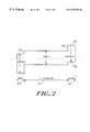
- FIG. 2illustrates an energy diagram of the detector 10 .
- E cis the conduction band edge and E V is the valence band edge.
- Potential barriersare formed between the intrinsic wafer 12 and the boundary layers 14 and 16 .
- the first potential barrier 40 from layer 12 to boundary layer 14extends upwardly.
- the upward extension in the potential barrier 40indicates the direction of increasing force against electron flow.
- the upward extension of the potential barrier 40opposes the flow of minority electrons from the layer 14 into the layer 12 .
- a second potential barrier 42is created at the transition from layer 12 to boundary layer 16 .
- the potential barrier 42extends downwardly.
- the downward extension of potential barrier 42indicates the direction of increasing force against the flow of holes.
- the downward extension of the potential barrier 42opposes the flow of minority carrier holes from the layer 16 into the layer 12 .
- the potential barriers resulting from the addition of the boundary layers 14 , 16create potential barriers not found in the prior art.
- the first potential barrier 40has been determined to have a bandgap of approximately 2.23 eV and the second potential barrier 42 has been determined to have a bandgap of approximately 2.42 eV.
- the potential barriers formed by the boundary layers 14 , 16dramatically reduce the leakage currents flowing through the detector 10 .
- FIG. 3illustrates a graph of current versus voltage for the P-I-N detector 10 when the detector was reverse biased with up to 1100 volts.
- the current and voltage measurements performed on the detectorshow clear diode-behavior.
- the graphalso illustrates that the P-I-N detector 10 has very low leakage current.
- the leakage current of the diodewas only 15 nA at 1000 volts. This leakage current is much lower than the leakage current obtained with an MSM device or any known P-I-N device of similar dimensions.
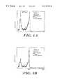
- FIGS. 4 and 5illustrate spectral response data for the P-I-N detector 10 when tested at room temperature using high energy radio nuclides and the resulting spectra. These figures clearly show the improved energy resolution and peak to valley ratio for the detector 10 .
- FIG. 4Ashows the spectral response for an MSM detector at 200 volts when exposed to Am-241 radiation.
- FIG. 4Bshows the spectral response for the P-I-N detector 10 at 300 volts when exposed to Am radiation.
- the peak in the response for the P-I-N detector at 60 keVrepresents the primary gamma ray of the Am-241 isotope being detected.
- FIG. 5Ashows the spectral response for an MSM detector at 200 volts when exposed to Co-57 radiation.
- FIG. 5Bshows the spectral response for the P-I-N detector 10 at 1100 volts when exposed to Co-57 radiation.
- the peak in the response for the P-I-N detector at 122 keVrepresents the primary gamma ray of the Co-57 isotope being detected.
- the best energy resolutionwas achieved with a bias voltage of 200 volts; beyond 200 volts of bias voltage the resolution for the MSM detector degraded due to increased leakage current-
- the energy resolution and peak-to-valley ratio of the P-I-N detector 10improved at voltages higher than 200 volts due to an enhanced electric field which increases the charge collection efficiency without suffering from additional leakage current.
- the detector 10is formed by first providing an intrinsic wafer 12 .
- the intrinsic wafercan be formed of a CdZnTe crystal.
- the CdZnTe crystalscan be grown using a High Pressure Bridgman approach (hereinafter “HPB”) or vertical Bridgman approach (hereinafter “VB”).
- HPBHigh Pressure Bridgman approach
- VBvertical Bridgman approach
- crystalsare grown near stoichiometry with respect to the metal-chalcogenide ratio, at temperatures near the maximum melting point.
- HPB methodprovides both a favorable growth temperature profile and an exceptionally clean, quartz-free growth enviromnent.
- the High Pressure Bridgman techniquecan be generalized to include the steps whereby cadmium telluride and zinc are loaded into a graphite crucible that in turn is loaded into a steel pressure vessel of a furnace. The temperature and pressure are then raised to 1100° C. and 100 atmospheres, respectively, and maintained for a period of several days while the crystal grows. After the waiting period, the temperature is slowly lowered until the system returns to ambient temperature and pressure, at which time the furnace is unloaded. The entire process can take up to approximately 28 days to complete. After growth of the crystals using the HPB method, the crystals forming the intrinsic wafer 12 may be etched in a 5% bromine/methanol solution to remove surface damage. Typically, those detectors having no internal defects are utilized in the detector 10 , while those CdZnTe crystals having internal flaws are either reworked or discarded.
- the CdZnTe intrinsic wafer 12can be purchased commercially. Companies known to market the crystal include Aurora Technologies Corporation of San Diego, Calif.; and EV Products, Division II-VI Company, Saxonburg, Pa.
- a first semiconductor boundary layer 16is formed on one surface of the intrinsic wafer 12 .
- the compounds forming the boundary layer 16are deposited on the intrinsic wafer 12 at a temperature below 150°.
- Exemplary deposition procedures used to form the boundary layer 16include electrodeposition, chemical vapor deposition, close spaced sublimation, solid-gas reaction, spray pyrolysis, sputtering, liquid phase epitaxy, molecular beam epitaxy, and other techniques well known in the art.
- the deposition process used in forming layer 16is carried out such that the temperature of the intrinsic wafer 12 does not rise to a level that degrades the detection capabilities of the intrinsic wafer. It is understood by the inventors that once the intrinsic wafer rises above 150° C., the detection capabilities of the intrinsic wafer can be permanently degraded.
- the boundary layer 16can be formed on the intrinsic wafer 12 while maintaining a temperature below 150° C., in accordance with the invention, by depositing the compounds in the layer 16 by thermal evaporation. By using thermal evaporation to deposit layer 16 , the intrinsic wafer 12 is maintained substantially at 125° C.
- FIG. 7illustrates the step of forming a doped layer 20 overlying the boundary layer 16 .
- the doped layer 20is formed by adding dopants to the surface of the boundary layer 16 .
- the doped section formed within layer 16becomes layer 20 .
- the doped layer 20extends from the top surface of layer 16 down to a predetermined depth in layer 16 .
- the addition of the dopant to layer 16forms a doped layer 20 that lies substantially parallel to the top surface of the underlying boundary layer 16 .
- a dopant, such as indium,can be added to the boundary layer 16 through a thermal evaporation process to form the doped layer 20 .
- FIG. 8illustrates the step of forming a second boundary layer 14 on the surface of layer 12 that opposes the boundary layer 16 .
- the compounds forming the second boundary layer 14are formed on the opposing surface of the intrinsic wafer 12 , while maintaining a temperature that does not degrade the detection abilities of the intrinsic wafer 12 . Typically, this requires that the boundary layer 14 is formed while maintaining the temperature of the intrinsic wafer at a temperature less than 150° C.
- the boundary layer 14can be formed while maintaining a low temperature by forming the layer 14 through a deposition process.
- Exemplary deposition procedures used to form the boundary layer 14include electrodeposition, chemical vapor deposition, close spaced sublimation, solid-gas reaction, spray pyrolysis, sputtering, liquid phase epitaxy, molecular beam epitaxy, and other techniques well known in the art.
- the boundary layer 14can be formed on the intrinsic wafer 12 while maintaining a temperature below 150° C., in accordance with the invention, by depositing the compounds in the layer 14 by thermal evaporation. By using thermal evaporation to deposit layer 14 , the intrinsic wafer 12 is maintained substantially at 125° C.
- FIG. 9illustrates the process of forming the doped layer 18 overlying the boundary layer 14 .
- the doped layer 18is formed by doping the upper surface of the boundary layer 14 .
- the doped section formed within layer 14becomes layer 18 .
- the doped layer 18extends from the top surface of layer 14 down to a predetermined depth in layer 14 .
- the addition of the dopant to layer 14forms a doped layer 18 that lies substantially parallel to the top surface of the underlying boundary layer 14 .
- a dopant, such as copper,can be added to the boundary layer 14 through a thermal evaporation process to form the doped layer 18 .
- the ohmic contacts 22 and 24 as shown in FIG. 1can be applied in various ways known in the art.
- the ohmic contact 22 that is in conductive contact with the P-type layer 18is formed from either gold, silver containing epoxy, indium-tin-oxide component or like materials depending upon the intended application.
- the ohmic contact 24 that is in conductive contact with the N-type layer 20may be formed from tin oxide, indium-tin-oxide, or a silver containing epoxy or like materials.
- CdZnTe crystalswere grown using a High Pressure Bridgeman method.
- the crystals grownhave a resistivity on the order of 10 10 ohms-cm.
- the CdZnTe crystalsPrior to the deposition of the CdS and ZnTe layers onto the CdZnTe layer, the CdZnTe crystals were etched in a bromine methanol solution and samples were immediately transferred to a vacuum evaporation system.
- an approximately 1 micron thick CdS layerwas deposited on the CdZnTe at a substrate temperature of 125° C. Thereafter, a 0.5 micron thick indium layer was evaporated as a contact layer to the CdS. On the other side of the CdZnTe crystal, an approximately 1 micron thick ZnTe layer was deposited. After the deposition of the ZnTe, the ZnTe layer was doped with copper that extended 0.25 micrometers into the underlying ZnTe boundary layer. Finally, a 0.5 micron thick gold layer was evaporated on the copper doped ZnTe layer as a contact layer. The ZnTe layer was evaporated at a substrate temperature of 100° C.
Landscapes
- Measurement Of Radiation (AREA)
- Light Receiving Elements (AREA)
Abstract
Description
Claims (14)
Priority Applications (1)
| Application Number | Priority Date | Filing Date | Title |
|---|---|---|---|
| US08/949,015US6255708B1 (en) | 1997-10-10 | 1997-10-10 | Semiconductor P-I-N detector |
Applications Claiming Priority (1)
| Application Number | Priority Date | Filing Date | Title |
|---|---|---|---|
| US08/949,015US6255708B1 (en) | 1997-10-10 | 1997-10-10 | Semiconductor P-I-N detector |
Publications (1)
| Publication Number | Publication Date |
|---|---|
| US6255708B1true US6255708B1 (en) | 2001-07-03 |
Family
ID=25488479
Family Applications (1)
| Application Number | Title | Priority Date | Filing Date |
|---|---|---|---|
| US08/949,015Expired - LifetimeUS6255708B1 (en) | 1997-10-10 | 1997-10-10 | Semiconductor P-I-N detector |
Country Status (1)
| Country | Link |
|---|---|
| US (1) | US6255708B1 (en) |
Cited By (266)
| Publication number | Priority date | Publication date | Assignee | Title |
|---|---|---|---|---|
| US20010029077A1 (en)* | 1997-07-08 | 2001-10-11 | Micron Technology, Inc. | Ultra high density flash memory |
| US6429065B2 (en) | 1998-04-14 | 2002-08-06 | Micron Technology, Inc. | Circuits and methods for a memory cell with a trench plate trench capacitor and a vertical bipolar read device |
| US6476434B1 (en) | 1997-07-08 | 2002-11-05 | Micron Tecnology, Inc. | 4 F2 folded bit line dram cell structure having buried bit and word lines |
| US6486027B1 (en) | 1998-02-27 | 2002-11-26 | Micron Technology, Inc. | Field programmable logic arrays with vertical transistors |
| US6498065B1 (en) | 1998-08-04 | 2002-12-24 | Micron Technology, Inc. | Memory address decode array with vertical transistors |
| US6504201B1 (en) | 1997-07-08 | 2003-01-07 | Micron Technology, Inc. | Memory cell having a vertical transistor with buried source/drain and dual gates |
| US6512233B1 (en)* | 2000-02-28 | 2003-01-28 | Shimadzu Corporation | Radiation detector and radiation image taking device |
| US6515510B2 (en) | 1998-08-04 | 2003-02-04 | Micron Technology, Inc. | Programmable logic array with vertical transistors |
| US6537871B2 (en) | 1997-10-06 | 2003-03-25 | Micron Technology, Inc. | Circuit and method for an open bit line memory cell with a vertical transistor and trench plate trench capacitor |
| US6597037B1 (en) | 1998-02-27 | 2003-07-22 | Micron Technology, Inc. | Programmable memory address decode array with vertical transistors |
| US20030142564A1 (en)* | 1997-10-06 | 2003-07-31 | Micron Technology, Inc. | Circuit and method for an open bit line memory cell with a vertical transistor and trench plate trench capacitor |
| US6680864B2 (en) | 1998-02-24 | 2004-01-20 | Micron Technology, Inc. | Method for reading a vertical gain cell and array for a dynamic random access memory |
| US6777744B2 (en) | 1998-02-24 | 2004-08-17 | Micron Technology, Inc. | Circuits and methods using vertical, complementary transistors |
| US6781132B2 (en) | 2001-08-10 | 2004-08-24 | The Regents Of The University Of Michigan | Collimated radiation detector assembly, array of collimated radiation detectors and collimated radiation detector module |
| US20050230620A1 (en)* | 2002-06-17 | 2005-10-20 | Marcus Jacka | Secondary electron detector, especially in a scanning electron microscope |
| US7057223B2 (en) | 1997-10-06 | 2006-06-06 | Micron Technology, Inc | Circuit and method for a folded bit line memory cell with vertical transistor and trench capacitor |
| US20060118728A1 (en)* | 2004-12-03 | 2006-06-08 | Bernard Phlips | Wafer bonded silicon radiation detectors |
| US7084451B2 (en)* | 1998-01-22 | 2006-08-01 | Micron Technology, Inc. | Circuits with a trench capacitor having micro-roughened semiconductor surfaces |
| US20080230709A1 (en)* | 2007-03-23 | 2008-09-25 | Tkaczyk J Eric | Energy discriminating detector different materials direct conversion layers |
| US20090001277A1 (en)* | 2007-06-29 | 2009-01-01 | The Regents Of The University Of Ca | GaTe semiconductor for radiation detection |
| US20090206670A1 (en)* | 2006-06-01 | 2009-08-20 | Exaflop Llc | Data Center Uninterruptible Power Distribution Architecture |
| US20090274266A1 (en)* | 2008-04-30 | 2009-11-05 | Yunfeng Sun | X-ray detector and x-ray ct apparatus |
| US20090294680A1 (en)* | 2008-05-28 | 2009-12-03 | Nikolic Rebecca J | Energy resolution in semiconductor gamma radiation detectors using heterojunctions and methods of use and preparation thereof |
| US20100015753A1 (en)* | 2008-07-17 | 2010-01-21 | James David Garnett | High Power Efficiency, Large Substrate, Polycrystalline CdTe Thin Film Semiconductor Photovoltaic Cell Structures Grown by Molecular Beam Epitaxy at High Deposition Rate for Use in Solar Electricity Generation |
| CN101022085B (en)* | 2007-03-12 | 2010-10-27 | 友达光电股份有限公司 | Semiconductor element and manufacturing method thereof |
| US20110139247A1 (en)* | 2009-12-16 | 2011-06-16 | Primestar Solar, Inc. | Graded alloy telluride layer in cadmium telluride thin film photovoltaic devices and methods of manufacturing the same |
| US20110139245A1 (en)* | 2009-12-16 | 2011-06-16 | Primestar Solar, Inc. | Thin film interlayer in cadmium telluride thin film photovoltaic devices and methods of manufacturing the same |
| US20110139249A1 (en)* | 2009-12-10 | 2011-06-16 | Uriel Solar Inc. | High Power Efficiency Polycrystalline CdTe Thin Film Semiconductor Photovoltaic Cell Structures for Use in Solar Electricity Generation |
| WO2011109425A1 (en)* | 2010-03-01 | 2011-09-09 | The Regents Of The University Of California | Silicon-on-insulator direct electron detector for low voltage electron microscopy |
| US8120683B1 (en)* | 1999-04-08 | 2012-02-21 | Nova R & D, Inc. | High resoultion digital imaging apparatus |
| US20120133009A1 (en)* | 2009-05-19 | 2012-05-31 | Takehisa Sasaki | Radiation detecting element and radiation detecting device |
| JP2015023203A (en)* | 2013-07-22 | 2015-02-02 | 株式会社島津製作所 | Manufacturing method of two-dimensional radiation detector |
| DE10308626B4 (en)* | 2003-02-27 | 2015-02-19 | Ketek Gmbh | Method of manufacturing semiconductor radiation detectors and semiconductor radiation detector |
| CN104779261A (en)* | 2014-01-14 | 2015-07-15 | 株式会社岛津制作所 | Radiation detector |
| US10159412B2 (en) | 2010-12-01 | 2018-12-25 | Cercacor Laboratories, Inc. | Handheld processing device including medical applications for minimally and non invasive glucose measurements |
| US10736518B2 (en) | 2015-08-31 | 2020-08-11 | Masimo Corporation | Systems and methods to monitor repositioning of a patient |
| US10765367B2 (en) | 2014-10-07 | 2020-09-08 | Masimo Corporation | Modular physiological sensors |
| US10779098B2 (en) | 2018-07-10 | 2020-09-15 | Masimo Corporation | Patient monitor alarm speaker analyzer |
| US10784634B2 (en) | 2015-02-06 | 2020-09-22 | Masimo Corporation | Pogo pin connector |
| USD897098S1 (en) | 2018-10-12 | 2020-09-29 | Masimo Corporation | Card holder set |
| US10799160B2 (en) | 2013-10-07 | 2020-10-13 | Masimo Corporation | Regional oximetry pod |
| US10799163B2 (en) | 2006-10-12 | 2020-10-13 | Masimo Corporation | Perfusion index smoother |
| US10825568B2 (en) | 2013-10-11 | 2020-11-03 | Masimo Corporation | Alarm notification system |
| US10849554B2 (en) | 2017-04-18 | 2020-12-01 | Masimo Corporation | Nose sensor |
| US10856788B2 (en) | 2005-03-01 | 2020-12-08 | Cercacor Laboratories, Inc. | Noninvasive multi-parameter patient monitor |
| US10856750B2 (en) | 2017-04-28 | 2020-12-08 | Masimo Corporation | Spot check measurement system |
| US10863938B2 (en) | 2006-10-12 | 2020-12-15 | Masimo Corporation | System and method for monitoring the life of a physiological sensor |
| US10869602B2 (en) | 2002-03-25 | 2020-12-22 | Masimo Corporation | Physiological measurement communications adapter |
| US10912500B2 (en) | 2008-07-03 | 2021-02-09 | Masimo Corporation | Multi-stream data collection system for noninvasive measurement of blood constituents |
| US10912524B2 (en) | 2006-09-22 | 2021-02-09 | Masimo Corporation | Modular patient monitor |
| US10918281B2 (en) | 2017-04-26 | 2021-02-16 | Masimo Corporation | Medical monitoring device having multiple configurations |
| US10925550B2 (en) | 2011-10-13 | 2021-02-23 | Masimo Corporation | Medical monitoring hub |
| US10932705B2 (en) | 2017-05-08 | 2021-03-02 | Masimo Corporation | System for displaying and controlling medical monitoring data |
| US10932729B2 (en) | 2018-06-06 | 2021-03-02 | Masimo Corporation | Opioid overdose monitoring |
| US10943450B2 (en) | 2009-12-21 | 2021-03-09 | Masimo Corporation | Modular patient monitor |
| US10939877B2 (en) | 2005-10-14 | 2021-03-09 | Masimo Corporation | Robust alarm system |
| US10952641B2 (en) | 2008-09-15 | 2021-03-23 | Masimo Corporation | Gas sampling line |
| US10956950B2 (en) | 2017-02-24 | 2021-03-23 | Masimo Corporation | Managing dynamic licenses for physiological parameters in a patient monitoring environment |
| US10959652B2 (en) | 2001-07-02 | 2021-03-30 | Masimo Corporation | Low power pulse oximeter |
| USD916135S1 (en) | 2018-10-11 | 2021-04-13 | Masimo Corporation | Display screen or portion thereof with a graphical user interface |
| US10973447B2 (en) | 2003-01-24 | 2021-04-13 | Masimo Corporation | Noninvasive oximetry optical sensor including disposable and reusable elements |
| US10980457B2 (en) | 2007-04-21 | 2021-04-20 | Masimo Corporation | Tissue profile wellness monitor |
| US10980432B2 (en) | 2013-08-05 | 2021-04-20 | Masimo Corporation | Systems and methods for measuring blood pressure |
| USD917704S1 (en) | 2019-08-16 | 2021-04-27 | Masimo Corporation | Patient monitor |
| US10987066B2 (en) | 2017-10-31 | 2021-04-27 | Masimo Corporation | System for displaying oxygen state indications |
| USD917564S1 (en) | 2018-10-11 | 2021-04-27 | Masimo Corporation | Display screen or portion thereof with graphical user interface |
| USD917550S1 (en) | 2018-10-11 | 2021-04-27 | Masimo Corporation | Display screen or portion thereof with a graphical user interface |
| US10991135B2 (en) | 2015-08-11 | 2021-04-27 | Masimo Corporation | Medical monitoring analysis and replay including indicia responsive to light attenuated by body tissue |
| US10993643B2 (en) | 2006-10-12 | 2021-05-04 | Masimo Corporation | Patient monitor capable of monitoring the quality of attached probes and accessories |
| US10993662B2 (en) | 2016-03-04 | 2021-05-04 | Masimo Corporation | Nose sensor |
| USD919094S1 (en) | 2019-08-16 | 2021-05-11 | Masimo Corporation | Blood pressure device |
| USD919100S1 (en) | 2019-08-16 | 2021-05-11 | Masimo Corporation | Holder for a patient monitor |
| US11000232B2 (en) | 2014-06-19 | 2021-05-11 | Masimo Corporation | Proximity sensor in pulse oximeter |
| US11022466B2 (en) | 2013-07-17 | 2021-06-01 | Masimo Corporation | Pulser with double-bearing position encoder for non-invasive physiological monitoring |
| USD921202S1 (en) | 2019-08-16 | 2021-06-01 | Masimo Corporation | Holder for a blood pressure device |
| US11020084B2 (en) | 2012-09-20 | 2021-06-01 | Masimo Corporation | Acoustic patient sensor coupler |
| US11020029B2 (en) | 2003-07-25 | 2021-06-01 | Masimo Corporation | Multipurpose sensor port |
| US11026604B2 (en) | 2017-07-13 | 2021-06-08 | Cercacor Laboratories, Inc. | Medical monitoring device for harmonizing physiological measurements |
| US11033210B2 (en) | 2008-03-04 | 2021-06-15 | Masimo Corporation | Multispot monitoring for use in optical coherence tomography |
| US11069461B2 (en) | 2012-08-01 | 2021-07-20 | Masimo Corporation | Automated assembly sensor cable |
| USD925597S1 (en) | 2017-10-31 | 2021-07-20 | Masimo Corporation | Display screen or portion thereof with graphical user interface |
| US11071480B2 (en) | 2012-04-17 | 2021-07-27 | Masimo Corporation | Hypersaturation index |
| US11076777B2 (en) | 2016-10-13 | 2021-08-03 | Masimo Corporation | Systems and methods for monitoring orientation to reduce pressure ulcer formation |
| US11086609B2 (en) | 2017-02-24 | 2021-08-10 | Masimo Corporation | Medical monitoring hub |
| US11083397B2 (en) | 2012-02-09 | 2021-08-10 | Masimo Corporation | Wireless patient monitoring device |
| US11087875B2 (en) | 2009-03-04 | 2021-08-10 | Masimo Corporation | Medical monitoring system |
| USD927699S1 (en) | 2019-10-18 | 2021-08-10 | Masimo Corporation | Electrode pad |
| US11089982B2 (en) | 2011-10-13 | 2021-08-17 | Masimo Corporation | Robust fractional saturation determination |
| US11095068B2 (en) | 2017-08-15 | 2021-08-17 | Masimo Corporation | Water resistant connector for noninvasive patient monitor |
| US11096631B2 (en) | 2017-02-24 | 2021-08-24 | Masimo Corporation | Modular multi-parameter patient monitoring device |
| US11103134B2 (en) | 2014-09-18 | 2021-08-31 | Masimo Semiconductor, Inc. | Enhanced visible near-infrared photodiode and non-invasive physiological sensor |
| US11109818B2 (en) | 2018-04-19 | 2021-09-07 | Masimo Corporation | Mobile patient alarm display |
| US11114188B2 (en) | 2009-10-06 | 2021-09-07 | Cercacor Laboratories, Inc. | System for monitoring a physiological parameter of a user |
| US11109770B2 (en) | 2011-06-21 | 2021-09-07 | Masimo Corporation | Patient monitoring system |
| US11132117B2 (en) | 2012-03-25 | 2021-09-28 | Masimo Corporation | Physiological monitor touchscreen interface |
| US11133105B2 (en) | 2009-03-04 | 2021-09-28 | Masimo Corporation | Medical monitoring system |
| US11145408B2 (en) | 2009-03-04 | 2021-10-12 | Masimo Corporation | Medical communication protocol translator |
| USD933232S1 (en) | 2020-05-11 | 2021-10-12 | Masimo Corporation | Blood pressure monitor |
| US11147518B1 (en) | 2013-10-07 | 2021-10-19 | Masimo Corporation | Regional oximetry signal processor |
| US11153089B2 (en) | 2016-07-06 | 2021-10-19 | Masimo Corporation | Secure and zero knowledge data sharing for cloud applications |
| US11176801B2 (en) | 2011-08-19 | 2021-11-16 | Masimo Corporation | Health care sanitation monitoring system |
| US11178776B2 (en) | 2015-02-06 | 2021-11-16 | Masimo Corporation | Fold flex circuit for LNOP |
| US11172890B2 (en) | 2012-01-04 | 2021-11-16 | Masimo Corporation | Automated condition screening and detection |
| US11179111B2 (en) | 2012-01-04 | 2021-11-23 | Masimo Corporation | Automated CCHD screening and detection |
| US11185262B2 (en) | 2017-03-10 | 2021-11-30 | Masimo Corporation | Pneumonia screener |
| US11191484B2 (en) | 2016-04-29 | 2021-12-07 | Masimo Corporation | Optical sensor tape |
| US11191485B2 (en) | 2006-06-05 | 2021-12-07 | Masimo Corporation | Parameter upgrade system |
| US11202571B2 (en) | 2016-07-07 | 2021-12-21 | Masimo Corporation | Wearable pulse oximeter and respiration monitor |
| US11224363B2 (en) | 2013-01-16 | 2022-01-18 | Masimo Corporation | Active-pulse blood analysis system |
| US11229374B2 (en) | 2006-12-09 | 2022-01-25 | Masimo Corporation | Plethysmograph variability processor |
| US11234655B2 (en) | 2007-01-20 | 2022-02-01 | Masimo Corporation | Perfusion trend indicator |
| US11241199B2 (en) | 2011-10-13 | 2022-02-08 | Masimo Corporation | System for displaying medical monitoring data |
| US11259745B2 (en) | 2014-01-28 | 2022-03-01 | Masimo Corporation | Autonomous drug delivery system |
| US11272852B2 (en) | 2011-06-21 | 2022-03-15 | Masimo Corporation | Patient monitoring system |
| US11272839B2 (en) | 2018-10-12 | 2022-03-15 | Ma Simo Corporation | System for transmission of sensor data using dual communication protocol |
| US11272883B2 (en) | 2016-03-04 | 2022-03-15 | Masimo Corporation | Physiological sensor |
| US11289199B2 (en) | 2010-01-19 | 2022-03-29 | Masimo Corporation | Wellness analysis system |
| US11291061B2 (en) | 2017-01-18 | 2022-03-29 | Masimo Corporation | Patient-worn wireless physiological sensor with pairing functionality |
| US11291415B2 (en) | 2015-05-04 | 2022-04-05 | Cercacor Laboratories, Inc. | Noninvasive sensor system with visual infographic display |
| USRE49007E1 (en) | 2010-03-01 | 2022-04-05 | Masimo Corporation | Adaptive alarm system |
| US11298021B2 (en) | 2017-10-19 | 2022-04-12 | Masimo Corporation | Medical monitoring system |
| USRE49034E1 (en) | 2002-01-24 | 2022-04-19 | Masimo Corporation | Physiological trend monitor |
| US11330996B2 (en) | 2010-05-06 | 2022-05-17 | Masimo Corporation | Patient monitor for determining microcirculation state |
| US11331013B2 (en) | 2014-09-04 | 2022-05-17 | Masimo Corporation | Total hemoglobin screening sensor |
| US11363960B2 (en) | 2011-02-25 | 2022-06-21 | Masimo Corporation | Patient monitor for monitoring microcirculation |
| US11367529B2 (en) | 2012-11-05 | 2022-06-21 | Cercacor Laboratories, Inc. | Physiological test credit method |
| US11389093B2 (en) | 2018-10-11 | 2022-07-19 | Masimo Corporation | Low noise oximetry cable |
| US11399722B2 (en) | 2010-03-30 | 2022-08-02 | Masimo Corporation | Plethysmographic respiration rate detection |
| US11399774B2 (en) | 2010-10-13 | 2022-08-02 | Masimo Corporation | Physiological measurement logic engine |
| US11410507B2 (en) | 2017-02-24 | 2022-08-09 | Masimo Corporation | Localized projection of audible noises in medical settings |
| US11406286B2 (en) | 2018-10-11 | 2022-08-09 | Masimo Corporation | Patient monitoring device with improved user interface |
| US11412964B2 (en) | 2008-05-05 | 2022-08-16 | Masimo Corporation | Pulse oximetry system with electrical decoupling circuitry |
| US11417426B2 (en) | 2017-02-24 | 2022-08-16 | Masimo Corporation | System for displaying medical monitoring data |
| US11426125B2 (en) | 2009-02-16 | 2022-08-30 | Masimo Corporation | Physiological measurement device |
| US11426104B2 (en) | 2004-08-11 | 2022-08-30 | Masimo Corporation | Method for data reduction and calibration of an OCT-based physiological monitor |
| US11439329B2 (en) | 2011-07-13 | 2022-09-13 | Masimo Corporation | Multiple measurement mode in a physiological sensor |
| US11445948B2 (en) | 2018-10-11 | 2022-09-20 | Masimo Corporation | Patient connector assembly with vertical detents |
| US11452449B2 (en) | 2012-10-30 | 2022-09-27 | Masimo Corporation | Universal medical system |
| US11464410B2 (en) | 2018-10-12 | 2022-10-11 | Masimo Corporation | Medical systems and methods |
| US11488715B2 (en) | 2011-02-13 | 2022-11-01 | Masimo Corporation | Medical characterization system |
| US11484231B2 (en) | 2010-03-08 | 2022-11-01 | Masimo Corporation | Reprocessing of a physiological sensor |
| US11500150B2 (en) | 2020-02-13 | 2022-11-15 | Electronics And Telecommunications Research Institute | Waveguide photodetector |
| US11504066B1 (en) | 2015-09-04 | 2022-11-22 | Cercacor Laboratories, Inc. | Low-noise sensor system |
| US11504058B1 (en) | 2016-12-02 | 2022-11-22 | Masimo Corporation | Multi-site noninvasive measurement of a physiological parameter |
| US11504002B2 (en) | 2012-09-20 | 2022-11-22 | Masimo Corporation | Physiological monitoring system |
| US11504062B2 (en) | 2013-03-14 | 2022-11-22 | Masimo Corporation | Patient monitor placement indicator |
| US11515664B2 (en) | 2009-03-11 | 2022-11-29 | Masimo Corporation | Magnetic connector |
| USD973072S1 (en) | 2020-09-30 | 2022-12-20 | Masimo Corporation | Display screen or portion thereof with graphical user interface |
| USD973686S1 (en) | 2020-09-30 | 2022-12-27 | Masimo Corporation | Display screen or portion thereof with graphical user interface |
| US11534087B2 (en) | 2009-11-24 | 2022-12-27 | Cercacor Laboratories, Inc. | Physiological measurement system with automatic wavelength adjustment |
| USD973685S1 (en) | 2020-09-30 | 2022-12-27 | Masimo Corporation | Display screen or portion thereof with graphical user interface |
| USD974193S1 (en) | 2020-07-27 | 2023-01-03 | Masimo Corporation | Wearable temperature measurement device |
| US11559275B2 (en) | 2008-12-30 | 2023-01-24 | Masimo Corporation | Acoustic sensor assembly |
| US11571152B2 (en) | 2009-12-04 | 2023-02-07 | Masimo Corporation | Calibration for multi-stage physiological monitors |
| US11581091B2 (en) | 2014-08-26 | 2023-02-14 | Vccb Holdings, Inc. | Real-time monitoring systems and methods in a healthcare environment |
| USD979516S1 (en) | 2020-05-11 | 2023-02-28 | Masimo Corporation | Connector |
| US11596363B2 (en) | 2013-09-12 | 2023-03-07 | Cercacor Laboratories, Inc. | Medical device management system |
| USD980091S1 (en) | 2020-07-27 | 2023-03-07 | Masimo Corporation | Wearable temperature measurement device |
| US11602289B2 (en) | 2015-02-06 | 2023-03-14 | Masimo Corporation | Soft boot pulse oximetry sensor |
| US11607139B2 (en) | 2006-09-20 | 2023-03-21 | Masimo Corporation | Congenital heart disease monitor |
| US11622733B2 (en) | 2008-05-02 | 2023-04-11 | Masimo Corporation | Monitor configuration system |
| US11637437B2 (en) | 2019-04-17 | 2023-04-25 | Masimo Corporation | Charging station for physiological monitoring device |
| US11638532B2 (en) | 2008-07-03 | 2023-05-02 | Masimo Corporation | User-worn device for noninvasively measuring a physiological parameter of a user |
| USD985498S1 (en) | 2019-08-16 | 2023-05-09 | Masimo Corporation | Connector |
| US11645905B2 (en) | 2013-03-13 | 2023-05-09 | Masimo Corporation | Systems and methods for monitoring a patient health network |
| US11653862B2 (en) | 2015-05-22 | 2023-05-23 | Cercacor Laboratories, Inc. | Non-invasive optical physiological differential pathlength sensor |
| US11673041B2 (en) | 2013-12-13 | 2023-06-13 | Masimo Corporation | Avatar-incentive healthcare therapy |
| US11672447B2 (en) | 2006-10-12 | 2023-06-13 | Masimo Corporation | Method and apparatus for calibration to reduce coupling between signals in a measurement system |
| US11679579B2 (en) | 2015-12-17 | 2023-06-20 | Masimo Corporation | Varnish-coated release liner |
| US11684296B2 (en) | 2018-12-21 | 2023-06-27 | Cercacor Laboratories, Inc. | Noninvasive physiological sensor |
| US11690574B2 (en) | 2003-11-05 | 2023-07-04 | Masimo Corporation | Pulse oximeter access apparatus and method |
| US11696712B2 (en) | 2014-06-13 | 2023-07-11 | Vccb Holdings, Inc. | Alarm fatigue management systems and methods |
| US11721105B2 (en) | 2020-02-13 | 2023-08-08 | Masimo Corporation | System and method for monitoring clinical activities |
| US11717210B2 (en) | 2010-09-28 | 2023-08-08 | Masimo Corporation | Depth of consciousness monitor including oximeter |
| US11724031B2 (en) | 2006-01-17 | 2023-08-15 | Masimo Corporation | Drug administration controller |
| US11730379B2 (en) | 2020-03-20 | 2023-08-22 | Masimo Corporation | Remote patient management and monitoring systems and methods |
| USD997365S1 (en) | 2021-06-24 | 2023-08-29 | Masimo Corporation | Physiological nose sensor |
| US11747178B2 (en) | 2011-10-27 | 2023-09-05 | Masimo Corporation | Physiological monitor gauge panel |
| US11744471B2 (en) | 2009-09-17 | 2023-09-05 | Masimo Corporation | Optical-based physiological monitoring system |
| USD998631S1 (en) | 2018-10-11 | 2023-09-12 | Masimo Corporation | Display screen or portion thereof with a graphical user interface |
| USD998630S1 (en) | 2018-10-11 | 2023-09-12 | Masimo Corporation | Display screen or portion thereof with a graphical user interface |
| US11752262B2 (en) | 2009-05-20 | 2023-09-12 | Masimo Corporation | Hemoglobin display and patient treatment |
| USD999246S1 (en) | 2018-10-11 | 2023-09-19 | Masimo Corporation | Display screen or portion thereof with a graphical user interface |
| US11766198B2 (en) | 2018-02-02 | 2023-09-26 | Cercacor Laboratories, Inc. | Limb-worn patient monitoring device |
| US11779247B2 (en) | 2009-07-29 | 2023-10-10 | Masimo Corporation | Non-invasive physiological sensor cover |
| USD1000975S1 (en) | 2021-09-22 | 2023-10-10 | Masimo Corporation | Wearable temperature measurement device |
| US11803623B2 (en) | 2019-10-18 | 2023-10-31 | Masimo Corporation | Display layout and interactive objects for patient monitoring |
| US11816771B2 (en) | 2017-02-24 | 2023-11-14 | Masimo Corporation | Augmented reality system for displaying patient data |
| US11832940B2 (en) | 2019-08-27 | 2023-12-05 | Cercacor Laboratories, Inc. | Non-invasive medical monitoring device for blood analyte measurements |
| US11864890B2 (en) | 2016-12-22 | 2024-01-09 | Cercacor Laboratories, Inc. | Methods and devices for detecting intensity of light with translucent detector |
| US11872156B2 (en) | 2018-08-22 | 2024-01-16 | Masimo Corporation | Core body temperature measurement |
| US11879960B2 (en) | 2020-02-13 | 2024-01-23 | Masimo Corporation | System and method for monitoring clinical activities |
| US11877824B2 (en) | 2011-08-17 | 2024-01-23 | Masimo Corporation | Modulated physiological sensor |
| US11887728B2 (en) | 2012-09-20 | 2024-01-30 | Masimo Corporation | Intelligent medical escalation process |
| US11883129B2 (en) | 2018-04-24 | 2024-01-30 | Cercacor Laboratories, Inc. | Easy insert finger sensor for transmission based spectroscopy sensor |
| US11937949B2 (en) | 2004-03-08 | 2024-03-26 | Masimo Corporation | Physiological parameter system |
| US11944431B2 (en) | 2006-03-17 | 2024-04-02 | Masimo Corportation | Apparatus and method for creating a stable optical interface |
| US11951186B2 (en) | 2019-10-25 | 2024-04-09 | Willow Laboratories, Inc. | Indicator compounds, devices comprising indicator compounds, and methods of making and using the same |
| US11963736B2 (en) | 2009-07-20 | 2024-04-23 | Masimo Corporation | Wireless patient monitoring system |
| US11963749B2 (en) | 2013-03-13 | 2024-04-23 | Masimo Corporation | Acoustic physiological monitoring system |
| US11974841B2 (en) | 2009-10-16 | 2024-05-07 | Masimo Corporation | Respiration processor |
| US11990706B2 (en) | 2012-02-08 | 2024-05-21 | Masimo Corporation | Cable tether system |
| US11986289B2 (en) | 2018-11-27 | 2024-05-21 | Willow Laboratories, Inc. | Assembly for medical monitoring device with multiple physiological sensors |
| US11986067B2 (en) | 2020-08-19 | 2024-05-21 | Masimo Corporation | Strap for a wearable device |
| US11992342B2 (en) | 2013-01-02 | 2024-05-28 | Masimo Corporation | Acoustic respiratory monitoring sensor with probe-off detection |
| US11998362B2 (en) | 2009-10-15 | 2024-06-04 | Masimo Corporation | Acoustic respiratory monitoring sensor having multiple sensing elements |
| US12004881B2 (en) | 2012-01-04 | 2024-06-11 | Masimo Corporation | Automated condition screening and detection |
| US12004869B2 (en) | 2018-11-05 | 2024-06-11 | Masimo Corporation | System to monitor and manage patient hydration via plethysmograph variablity index in response to the passive leg raising |
| US12014328B2 (en) | 2005-07-13 | 2024-06-18 | Vccb Holdings, Inc. | Medicine bottle cap with electronic embedded curved display |
| USD1031729S1 (en) | 2017-08-15 | 2024-06-18 | Masimo Corporation | Connector |
| US12016721B2 (en) | 2013-10-11 | 2024-06-25 | Masimo Corporation | Acoustic sensor with attachment portion |
| US12016661B2 (en) | 2011-01-10 | 2024-06-25 | Masimo Corporation | Non-invasive intravascular volume index monitor |
| US12029586B2 (en) | 2006-10-12 | 2024-07-09 | Masimo Corporation | Oximeter probe off indicator defining probe off space |
| US12029844B2 (en) | 2020-06-25 | 2024-07-09 | Willow Laboratories, Inc. | Combination spirometer-inhaler |
| US12036014B2 (en) | 2015-01-23 | 2024-07-16 | Masimo Corporation | Nasal/oral cannula system and manufacturing |
| US12042285B1 (en) | 2012-08-29 | 2024-07-23 | Masimo Corporation | Physiological measurement calibration |
| USD1036293S1 (en) | 2021-08-17 | 2024-07-23 | Masimo Corporation | Straps for a wearable device |
| US12048534B2 (en) | 2020-03-04 | 2024-07-30 | Willow Laboratories, Inc. | Systems and methods for securing a tissue site to a sensor |
| US12066426B1 (en) | 2019-01-16 | 2024-08-20 | Masimo Corporation | Pulsed micro-chip laser for malaria detection |
| US12076159B2 (en) | 2019-02-07 | 2024-09-03 | Masimo Corporation | Combining multiple QEEG features to estimate drug-independent sedation level using machine learning |
| US12082926B2 (en) | 2020-08-04 | 2024-09-10 | Masimo Corporation | Optical sensor with multiple detectors or multiple emitters |
| USD1041511S1 (en) | 2018-10-11 | 2024-09-10 | Masimo Corporation | Display screen or portion thereof with a graphical user interface |
| USD1042596S1 (en) | 2022-12-12 | 2024-09-17 | Masimo Corporation | Monitoring camera |
| US12089968B2 (en) | 2006-12-22 | 2024-09-17 | Masimo Corporation | Optical patient monitor |
| US12097043B2 (en) | 2018-06-06 | 2024-09-24 | Masimo Corporation | Locating a locally stored medication |
| US12114974B2 (en) | 2020-01-13 | 2024-10-15 | Masimo Corporation | Wearable device with physiological parameters monitoring |
| USD1048571S1 (en) | 2021-10-07 | 2024-10-22 | Masimo Corporation | Bite block |
| US12126683B2 (en) | 2021-08-31 | 2024-10-22 | Masimo Corporation | Privacy switch for mobile communications device |
| US12131661B2 (en) | 2019-10-03 | 2024-10-29 | Willow Laboratories, Inc. | Personalized health coaching system |
| US12128213B2 (en) | 2020-01-30 | 2024-10-29 | Willow Laboratories, Inc. | Method of operating redundant staggered disease management systems |
| US12127838B2 (en) | 2020-04-22 | 2024-10-29 | Willow Laboratories, Inc. | Self-contained minimal action invasive blood constituent system |
| USD1048908S1 (en) | 2022-10-04 | 2024-10-29 | Masimo Corporation | Wearable sensor |
| US12138079B2 (en) | 2016-11-30 | 2024-11-12 | Masimo Corporation | Haemodynamic monitor with improved filtering |
| US12178572B1 (en) | 2013-06-11 | 2024-12-31 | Masimo Corporation | Blood glucose sensing system |
| US12178852B2 (en) | 2020-09-30 | 2024-12-31 | Willow Laboratories, Inc. | Insulin formulations and uses in infusion devices |
| USD1057160S1 (en) | 2022-03-29 | 2025-01-07 | Masimo Corporation | Electronic measurement device |
| USD1057159S1 (en) | 2022-03-29 | 2025-01-07 | Masimo Corporation | Electronic measurement device |
| US12198790B1 (en) | 2010-10-07 | 2025-01-14 | Masimo Corporation | Physiological monitor sensor systems and methods |
| US12201702B1 (en) | 2016-02-12 | 2025-01-21 | Masimo Corporation | Diagnosis, removal, or mechanical damaging of tumor using plasmonic nanobubbles |
| US12207901B1 (en) | 2019-08-16 | 2025-01-28 | Masimo Corporation | Optical detection of transient vapor nanobubbles in a microfluidic device |
| USD1061585S1 (en) | 2020-10-16 | 2025-02-11 | Masimo Corporation | Display screen or portion thereof with graphical user interface |
| US12220207B2 (en) | 2019-02-26 | 2025-02-11 | Masimo Corporation | Non-contact core body temperature measurement systems and methods |
| USD1063893S1 (en) | 2022-03-11 | 2025-02-25 | Masimo Corporation | Electronic device |
| US12236767B2 (en) | 2022-01-11 | 2025-02-25 | Masimo Corporation | Machine learning based monitoring system |
| USD1066244S1 (en) | 2023-05-11 | 2025-03-11 | Masimo Corporation | Charger |
| US12257081B2 (en) | 2009-10-15 | 2025-03-25 | Masimo Corporation | Bidirectional physiological information display |
| USD1068656S1 (en) | 2023-05-11 | 2025-04-01 | Masimo Corporation | Charger |
| US12272445B1 (en) | 2019-12-05 | 2025-04-08 | Masimo Corporation | Automated medical coding |
| USD1071195S1 (en) | 2022-10-06 | 2025-04-15 | Masimo Corporation | Mounting device for a medical transducer |
| USD1072837S1 (en) | 2020-10-27 | 2025-04-29 | Masimo Corporation | Display screen or portion thereof with graphical user interface |
| USD1072836S1 (en) | 2020-10-16 | 2025-04-29 | Masimo Corporation | Display screen or portion thereof with graphical user interface |
| USD1078689S1 (en) | 2022-12-12 | 2025-06-10 | Masimo Corporation | Electronic device |
| US12336796B2 (en) | 2021-07-13 | 2025-06-24 | Masimo Corporation | Wearable device with physiological parameters monitoring |
| US12343108B2 (en) | 2013-03-15 | 2025-07-01 | Willow Laboratories, Inc. | Cloud-based physiological monitoring system |
| USD1083653S1 (en) | 2022-09-09 | 2025-07-15 | Masimo Corporation | Band |
| US12362596B2 (en) | 2021-08-19 | 2025-07-15 | Masimo Corporation | Wearable physiological monitoring devices |
| USD1085102S1 (en) | 2021-03-19 | 2025-07-22 | Masimo Corporation | Display screen or portion thereof with graphical user interface |
| US12367973B2 (en) | 2013-09-12 | 2025-07-22 | Willow Laboratories, Inc. | Medical device calibration |
| US12383194B2 (en) | 2012-06-07 | 2025-08-12 | Masimo Corporation | Depth of consciousness monitor |
| US12408869B2 (en) | 2009-05-19 | 2025-09-09 | Masimo Corporation | Disposable components for reusable physiological sensor |
| USD1092244S1 (en) | 2023-07-03 | 2025-09-09 | Masimo Corporation | Band for an electronic device |
| US12419588B2 (en) | 2009-10-15 | 2025-09-23 | Masimo Corporation | System and method for monitoring respiratory rate measurements |
| USD1094735S1 (en) | 2023-05-25 | 2025-09-23 | Masimo Corporation | Wearable device for physiological monitoring |
| USD1095288S1 (en) | 2022-07-20 | 2025-09-30 | Masimo Corporation | Set of straps for a wearable device |
| USD1095483S1 (en) | 2022-09-23 | 2025-09-30 | Masimo Corporation | Caregiver notification device |
| US12440171B2 (en) | 2021-01-05 | 2025-10-14 | Masimo Corporation | Modular patient monitor |
Citations (7)
| Publication number | Priority date | Publication date | Assignee | Title |
|---|---|---|---|---|
| US4977097A (en) | 1986-10-21 | 1990-12-11 | Ametek, Inc. | Method of making heterojunction P-I-N photovoltaic cell |
| US5117114A (en)* | 1989-12-11 | 1992-05-26 | The Regents Of The University Of California | High resolution amorphous silicon radiation detectors |
| US5391882A (en) | 1993-06-11 | 1995-02-21 | Santa Barbara Research Center | Semiconductor gamma ray detector including compositionally graded, leakage current blocking potential barrier layers and method of fabricating the detector |
| US5512756A (en)* | 1993-12-23 | 1996-04-30 | Siemens Aktiengesellschaft | X-ray detector with direct conversion |
| US5528495A (en) | 1993-09-01 | 1996-06-18 | Schlumberger Technology Corporation | Cadmium zinc telluride borehole detector |
| US5616925A (en)* | 1995-06-07 | 1997-04-01 | Santa Barbara Research Center | Gamma ray detector with improved resolution and method of fabrication |
| US5627377A (en)* | 1995-09-07 | 1997-05-06 | Santa Barbara Research Center | Single carrier-type solid-state radiation detector device |
- 1997
- 1997-10-10USUS08/949,015patent/US6255708B1/ennot_activeExpired - Lifetime
Patent Citations (7)
| Publication number | Priority date | Publication date | Assignee | Title |
|---|---|---|---|---|
| US4977097A (en) | 1986-10-21 | 1990-12-11 | Ametek, Inc. | Method of making heterojunction P-I-N photovoltaic cell |
| US5117114A (en)* | 1989-12-11 | 1992-05-26 | The Regents Of The University Of California | High resolution amorphous silicon radiation detectors |
| US5391882A (en) | 1993-06-11 | 1995-02-21 | Santa Barbara Research Center | Semiconductor gamma ray detector including compositionally graded, leakage current blocking potential barrier layers and method of fabricating the detector |
| US5528495A (en) | 1993-09-01 | 1996-06-18 | Schlumberger Technology Corporation | Cadmium zinc telluride borehole detector |
| US5512756A (en)* | 1993-12-23 | 1996-04-30 | Siemens Aktiengesellschaft | X-ray detector with direct conversion |
| US5616925A (en)* | 1995-06-07 | 1997-04-01 | Santa Barbara Research Center | Gamma ray detector with improved resolution and method of fabrication |
| US5627377A (en)* | 1995-09-07 | 1997-05-06 | Santa Barbara Research Center | Single carrier-type solid-state radiation detector device |
Non-Patent Citations (6)
| Title |
|---|
| Åbro, E. and Johansen, G.A., "Low Noise Gamma-ray and X-ray Detectors Based on CdTe-materials," Nuclear Instruments and Methods in Physics Research, vol. A 377, 470-4 (1996). |
| Åbro, E. and Johansen, G.A., "Low Noise Gamma-ray and X-ray Detectors Based on CdTe-materials," Nuclear Instruments and Methods in Physics Research, vol. A 377, 470-4 (1996). |
| Butler, J.F. et al., "Cd1-xZnxTe Gamma Ray Detectors," IEEE Transactions on Nuclear Science, vol. 39, No. 4, 605-9 (1992). |
| Hazlett, T. et al., "Large, High Resolution CdTe Gamma Ray Sensors," IEEE Transactions on Nuclear Science, vol. 33, No. 1, 332-5 (1986). |
| Parnham, K., "Recent Progress in Cd1-xZnxTe Radiation Detectors," Nuclear Instruments and Methods in Physics Research, vol. A 377, 487-91 (1996). |
| Ryan, F.J. et al., "Gamma Ray Detectors with HgCdTe Contact Layers," Appl. Phys. Lett., vol. 46, No. 3, 274-6 (1985). |
Cited By (490)
| Publication number | Priority date | Publication date | Assignee | Title |
|---|---|---|---|---|
| US20060258096A1 (en)* | 1997-07-08 | 2006-11-16 | Micron Technology, Inc. | Ultra high density flash memory |
| US20070069281A1 (en)* | 1997-07-08 | 2007-03-29 | Micron Technology, Inc. | Ultra high density flash memory |
| US6476434B1 (en) | 1997-07-08 | 2002-11-05 | Micron Tecnology, Inc. | 4 F2 folded bit line dram cell structure having buried bit and word lines |
| US6818937B2 (en) | 1997-07-08 | 2004-11-16 | Micron Technology, Inc. | Memory cell having a vertical transistor with buried source/drain and dual gates |
| US20060255397A1 (en)* | 1997-07-08 | 2006-11-16 | Micron Technology, Inc. | Ultra high density flash memory |
| US6504201B1 (en) | 1997-07-08 | 2003-01-07 | Micron Technology, Inc. | Memory cell having a vertical transistor with buried source/drain and dual gates |
| US20010029077A1 (en)* | 1997-07-08 | 2001-10-11 | Micron Technology, Inc. | Ultra high density flash memory |
| US7057223B2 (en) | 1997-10-06 | 2006-06-06 | Micron Technology, Inc | Circuit and method for a folded bit line memory cell with vertical transistor and trench capacitor |
| US6537871B2 (en) | 1997-10-06 | 2003-03-25 | Micron Technology, Inc. | Circuit and method for an open bit line memory cell with a vertical transistor and trench plate trench capacitor |
| US6798009B2 (en) | 1997-10-06 | 2004-09-28 | Micron Technology, Inc. | Circuit and method for an open bit line memory cell with a vertical transistor and trench plate trench capacitor |
| US20030142564A1 (en)* | 1997-10-06 | 2003-07-31 | Micron Technology, Inc. | Circuit and method for an open bit line memory cell with a vertical transistor and trench plate trench capacitor |
| US7223678B2 (en) | 1997-10-06 | 2007-05-29 | Micron Technology, Inc. | Circuit and method for a folded bit line memory cell with vertical transistor and trench capacitor |
| US7084451B2 (en)* | 1998-01-22 | 2006-08-01 | Micron Technology, Inc. | Circuits with a trench capacitor having micro-roughened semiconductor surfaces |
| US7408216B2 (en) | 1998-01-22 | 2008-08-05 | Micron Technology, Inc. | Device, system, and method for a trench capacitor having micro-roughened semiconductor surfaces |
| US6777744B2 (en) | 1998-02-24 | 2004-08-17 | Micron Technology, Inc. | Circuits and methods using vertical, complementary transistors |
| US20040132232A1 (en)* | 1998-02-24 | 2004-07-08 | Micron Technology, Inc. | Vertical gain cell and array for a dynamic random access memory and method for forming the same |
| US6756622B2 (en) | 1998-02-24 | 2004-06-29 | Micron Technology, Inc. | Vertical gain cell and array for a dynamic random access memory and method for forming the same |
| US7049196B2 (en) | 1998-02-24 | 2006-05-23 | Micron Technology, Inc. | Vertical gain cell and array for a dynamic random access memory and method for forming the same |
| US6680864B2 (en) | 1998-02-24 | 2004-01-20 | Micron Technology, Inc. | Method for reading a vertical gain cell and array for a dynamic random access memory |
| US6812516B2 (en) | 1998-02-27 | 2004-11-02 | Micron Technology, Inc. | Field programmable logic arrays with vertical transistors |
| US6486027B1 (en) | 1998-02-27 | 2002-11-26 | Micron Technology, Inc. | Field programmable logic arrays with vertical transistors |
| US6597037B1 (en) | 1998-02-27 | 2003-07-22 | Micron Technology, Inc. | Programmable memory address decode array with vertical transistors |
| US6429065B2 (en) | 1998-04-14 | 2002-08-06 | Micron Technology, Inc. | Circuits and methods for a memory cell with a trench plate trench capacitor and a vertical bipolar read device |
| US6515510B2 (en) | 1998-08-04 | 2003-02-04 | Micron Technology, Inc. | Programmable logic array with vertical transistors |
| US6747305B2 (en) | 1998-08-04 | 2004-06-08 | Micron Technology, Inc. | Memory address decode array with vertical transistors |
| US6498065B1 (en) | 1998-08-04 | 2002-12-24 | Micron Technology, Inc. | Memory address decode array with vertical transistors |
| US8120683B1 (en)* | 1999-04-08 | 2012-02-21 | Nova R & D, Inc. | High resoultion digital imaging apparatus |
| US6512233B1 (en)* | 2000-02-28 | 2003-01-28 | Shimadzu Corporation | Radiation detector and radiation image taking device |
| US10959652B2 (en) | 2001-07-02 | 2021-03-30 | Masimo Corporation | Low power pulse oximeter |
| US11219391B2 (en) | 2001-07-02 | 2022-01-11 | Masimo Corporation | Low power pulse oximeter |
| US10980455B2 (en) | 2001-07-02 | 2021-04-20 | Masimo Corporation | Low power pulse oximeter |
| US6781132B2 (en) | 2001-08-10 | 2004-08-24 | The Regents Of The University Of Michigan | Collimated radiation detector assembly, array of collimated radiation detectors and collimated radiation detector module |
| USRE49034E1 (en) | 2002-01-24 | 2022-04-19 | Masimo Corporation | Physiological trend monitor |
| US10869602B2 (en) | 2002-03-25 | 2020-12-22 | Masimo Corporation | Physiological measurement communications adapter |
| US11484205B2 (en) | 2002-03-25 | 2022-11-01 | Masimo Corporation | Physiological measurement device |
| US20050230620A1 (en)* | 2002-06-17 | 2005-10-20 | Marcus Jacka | Secondary electron detector, especially in a scanning electron microscope |
| US7193222B2 (en)* | 2002-06-17 | 2007-03-20 | Tescan S.R.O. | Secondary electron detector, especially in a scanning electron microscope |
| US10973447B2 (en) | 2003-01-24 | 2021-04-13 | Masimo Corporation | Noninvasive oximetry optical sensor including disposable and reusable elements |
| DE10308626B4 (en)* | 2003-02-27 | 2015-02-19 | Ketek Gmbh | Method of manufacturing semiconductor radiation detectors and semiconductor radiation detector |
| US11020029B2 (en) | 2003-07-25 | 2021-06-01 | Masimo Corporation | Multipurpose sensor port |
| US11690574B2 (en) | 2003-11-05 | 2023-07-04 | Masimo Corporation | Pulse oximeter access apparatus and method |
| US11937949B2 (en) | 2004-03-08 | 2024-03-26 | Masimo Corporation | Physiological parameter system |
| US11426104B2 (en) | 2004-08-11 | 2022-08-30 | Masimo Corporation | Method for data reduction and calibration of an OCT-based physiological monitor |
| US20060118728A1 (en)* | 2004-12-03 | 2006-06-08 | Bernard Phlips | Wafer bonded silicon radiation detectors |
| US10984911B2 (en) | 2005-03-01 | 2021-04-20 | Cercacor Laboratories, Inc. | Multiple wavelength sensor emitters |
| US12283374B2 (en) | 2005-03-01 | 2025-04-22 | Willow Laboratories, Inc. | Noninvasive multi-parameter patient monitor |
| US12230393B2 (en) | 2005-03-01 | 2025-02-18 | Willow Laboratories, Inc. | Multiple wavelength sensor emitters |
| US11545263B2 (en) | 2005-03-01 | 2023-01-03 | Cercacor Laboratories, Inc. | Multiple wavelength sensor emitters |
| US11430572B2 (en) | 2005-03-01 | 2022-08-30 | Cercacor Laboratories, Inc. | Multiple wavelength sensor emitters |
| US10856788B2 (en) | 2005-03-01 | 2020-12-08 | Cercacor Laboratories, Inc. | Noninvasive multi-parameter patient monitor |
| US12014328B2 (en) | 2005-07-13 | 2024-06-18 | Vccb Holdings, Inc. | Medicine bottle cap with electronic embedded curved display |
| US10939877B2 (en) | 2005-10-14 | 2021-03-09 | Masimo Corporation | Robust alarm system |
| US12178620B2 (en) | 2005-10-14 | 2024-12-31 | Masimo Corporation | Robust alarm system |
| US11839498B2 (en) | 2005-10-14 | 2023-12-12 | Masimo Corporation | Robust alarm system |
| US11724031B2 (en) | 2006-01-17 | 2023-08-15 | Masimo Corporation | Drug administration controller |
| US11944431B2 (en) | 2006-03-17 | 2024-04-02 | Masimo Corportation | Apparatus and method for creating a stable optical interface |
| US20090206670A1 (en)* | 2006-06-01 | 2009-08-20 | Exaflop Llc | Data Center Uninterruptible Power Distribution Architecture |
| US11191485B2 (en) | 2006-06-05 | 2021-12-07 | Masimo Corporation | Parameter upgrade system |
| US12109048B2 (en) | 2006-06-05 | 2024-10-08 | Masimo Corporation | Parameter upgrade system |
| US11607139B2 (en) | 2006-09-20 | 2023-03-21 | Masimo Corporation | Congenital heart disease monitor |
| US10912524B2 (en) | 2006-09-22 | 2021-02-09 | Masimo Corporation | Modular patient monitor |
| US11857319B2 (en) | 2006-10-12 | 2024-01-02 | Masimo Corporation | System and method for monitoring the life of a physiological sensor |
| US12127835B2 (en) | 2006-10-12 | 2024-10-29 | Masimo Corporation | System and method for monitoring the life of a physiological sensor |
| US10993643B2 (en) | 2006-10-12 | 2021-05-04 | Masimo Corporation | Patient monitor capable of monitoring the quality of attached probes and accessories |
| US12029586B2 (en) | 2006-10-12 | 2024-07-09 | Masimo Corporation | Oximeter probe off indicator defining probe off space |
| US11317837B2 (en) | 2006-10-12 | 2022-05-03 | Masimo Corporation | System and method for monitoring the life of a physiological sensor |
| US11006867B2 (en) | 2006-10-12 | 2021-05-18 | Masimo Corporation | Perfusion index smoother |
| US11759130B2 (en) | 2006-10-12 | 2023-09-19 | Masimo Corporation | Perfusion index smoother |
| US12171552B2 (en) | 2006-10-12 | 2024-12-24 | Masimo Corporation | Method and apparatus for calibration to reduce coupling between signals in a measurement system |
| US11672447B2 (en) | 2006-10-12 | 2023-06-13 | Masimo Corporation | Method and apparatus for calibration to reduce coupling between signals in a measurement system |
| US10799163B2 (en) | 2006-10-12 | 2020-10-13 | Masimo Corporation | Perfusion index smoother |
| US10863938B2 (en) | 2006-10-12 | 2020-12-15 | Masimo Corporation | System and method for monitoring the life of a physiological sensor |
| US11857315B2 (en) | 2006-10-12 | 2024-01-02 | Masimo Corporation | Patient monitor capable of monitoring the quality of attached probes and accessories |
| US12109012B2 (en) | 2006-12-09 | 2024-10-08 | Masimo Corporation | Plethysmograph variability processor |
| US11229374B2 (en) | 2006-12-09 | 2022-01-25 | Masimo Corporation | Plethysmograph variability processor |
| US12357243B2 (en) | 2006-12-22 | 2025-07-15 | Masimo Corporation | Physiological parameter system |
| US12089968B2 (en) | 2006-12-22 | 2024-09-17 | Masimo Corporation | Optical patient monitor |
| US11234655B2 (en) | 2007-01-20 | 2022-02-01 | Masimo Corporation | Perfusion trend indicator |
| CN101022085B (en)* | 2007-03-12 | 2010-10-27 | 友达光电股份有限公司 | Semiconductor element and manufacturing method thereof |
| US20080230709A1 (en)* | 2007-03-23 | 2008-09-25 | Tkaczyk J Eric | Energy discriminating detector different materials direct conversion layers |
| US7573040B2 (en)* | 2007-03-23 | 2009-08-11 | General Electric Company | Energy discriminating detector different materials direct conversion layers |
| US12156733B2 (en) | 2007-04-21 | 2024-12-03 | Masimo Corporation | Tissue profile wellness monitor |
| US11647923B2 (en) | 2007-04-21 | 2023-05-16 | Masimo Corporation | Tissue profile wellness monitor |
| US10980457B2 (en) | 2007-04-21 | 2021-04-20 | Masimo Corporation | Tissue profile wellness monitor |
| US20090001277A1 (en)* | 2007-06-29 | 2009-01-01 | The Regents Of The University Of Ca | GaTe semiconductor for radiation detection |
| US7550735B2 (en)* | 2007-06-29 | 2009-06-23 | Lawrence Livermore National Security, Llc | GaTe semiconductor for radiation detection |
| US11033210B2 (en) | 2008-03-04 | 2021-06-15 | Masimo Corporation | Multispot monitoring for use in optical coherence tomography |
| US11660028B2 (en) | 2008-03-04 | 2023-05-30 | Masimo Corporation | Multispot monitoring for use in optical coherence tomography |
| US20090274266A1 (en)* | 2008-04-30 | 2009-11-05 | Yunfeng Sun | X-ray detector and x-ray ct apparatus |
| CN101569530B (en)* | 2008-04-30 | 2013-03-27 | Ge医疗系统环球技术有限公司 | X-ray detector and x-ray ct equipment |
| US7916831B2 (en) | 2008-04-30 | 2011-03-29 | Ge Medical Systems Global Technology Company, Llc | X-ray detector and X-ray CT apparatus |
| US11622733B2 (en) | 2008-05-02 | 2023-04-11 | Masimo Corporation | Monitor configuration system |
| US11412964B2 (en) | 2008-05-05 | 2022-08-16 | Masimo Corporation | Pulse oximetry system with electrical decoupling circuitry |
| US20090294680A1 (en)* | 2008-05-28 | 2009-12-03 | Nikolic Rebecca J | Energy resolution in semiconductor gamma radiation detectors using heterojunctions and methods of use and preparation thereof |
| US8258482B2 (en)* | 2008-05-28 | 2012-09-04 | Lawrence Livermore National Security, Llc | Energy resolution in semiconductor gamma radiation detectors using heterojunctions and methods of use and preparation thereof |
| US11484230B2 (en) | 2008-07-03 | 2022-11-01 | Masimo Corporation | User-worn device for noninvasively measuring a physiological parameter of a user |
| US11647914B2 (en) | 2008-07-03 | 2023-05-16 | Masimo Corporation | User-worn device for noninvasively measuring a physiological parameter of a user |
| US11751773B2 (en) | 2008-07-03 | 2023-09-12 | Masimo Corporation | Emitter arrangement for physiological measurements |
| US10912500B2 (en) | 2008-07-03 | 2021-02-09 | Masimo Corporation | Multi-stream data collection system for noninvasive measurement of blood constituents |
| US12036009B1 (en) | 2008-07-03 | 2024-07-16 | Masimo Corporation | User-worn device for noninvasively measuring a physiological parameter of a user |
| US12023139B1 (en) | 2008-07-03 | 2024-07-02 | Masimo Corporation | User-worn device for noninvasively measuring a physiological parameter of a user |
| US10912501B2 (en) | 2008-07-03 | 2021-02-09 | Masimo Corporation | User-worn device for noninvasively measuring a physiological parameter of a user |
| US11426103B2 (en) | 2008-07-03 | 2022-08-30 | Masimo Corporation | Multi-stream data collection system for noninvasive measurement of blood constituents |
| US10912502B2 (en) | 2008-07-03 | 2021-02-09 | Masimo Corporation | User-worn device for noninvasively measuring a physiological parameter of a user |
| US11484229B2 (en) | 2008-07-03 | 2022-11-01 | Masimo Corporation | User-worn device for noninvasively measuring a physiological parameter of a user |
| US11638532B2 (en) | 2008-07-03 | 2023-05-02 | Masimo Corporation | User-worn device for noninvasively measuring a physiological parameter of a user |
| US11642036B2 (en) | 2008-07-03 | 2023-05-09 | Masimo Corporation | User-worn device for noninvasively measuring a physiological parameter of a user |
| US10945648B2 (en) | 2008-07-03 | 2021-03-16 | Masimo Corporation | User-worn device for noninvasively measuring a physiological parameter of a user |
| US11642037B2 (en) | 2008-07-03 | 2023-05-09 | Masimo Corporation | User-worn device for noninvasively measuring a physiological parameter of a user |
| US8298856B2 (en) | 2008-07-17 | 2012-10-30 | Uriel Solar, Inc. | Polycrystalline CDTE thin film semiconductor photovoltaic cell structures for use in solar electricity generation |
| US8828783B2 (en) | 2008-07-17 | 2014-09-09 | Uriel Solar, Inc. | Polycrystalline CDTE thin film semiconductor photovoltaic cell structures for use in solar electricity generation |
| US8580602B2 (en) | 2008-07-17 | 2013-11-12 | Uriel Solar, Inc. | Polycrystalline CDTE thin film semiconductor photovoltaic cell structures for use in solar electricity generation |
| US9190555B2 (en) | 2008-07-17 | 2015-11-17 | Uriel Solar, Inc. | Polycrystalline CdTe thin film semiconductor photovoltaic cell structures for use in solar electricity generation |
| US20100015753A1 (en)* | 2008-07-17 | 2010-01-21 | James David Garnett | High Power Efficiency, Large Substrate, Polycrystalline CdTe Thin Film Semiconductor Photovoltaic Cell Structures Grown by Molecular Beam Epitaxy at High Deposition Rate for Use in Solar Electricity Generation |
| US20100012188A1 (en)* | 2008-07-17 | 2010-01-21 | James David Garnett | High Power Efficiency, Large Substrate, Polycrystalline CdTe Thin Film Semiconductor Photovoltaic Cell Structures Grown by Molecular Beam Epitaxy at High Deposition Rate for Use in Solar Electricity Generation |
| US8664524B2 (en) | 2008-07-17 | 2014-03-04 | Uriel Solar, Inc. | High power efficiency, large substrate, polycrystalline CdTe thin film semiconductor photovoltaic cell structures grown by molecular beam epitaxy at high deposition rate for use in solar electricity generation |
| US12414711B2 (en) | 2008-09-15 | 2025-09-16 | Masimo Corporation | Gas sampling line |
| US11564593B2 (en) | 2008-09-15 | 2023-01-31 | Masimo Corporation | Gas sampling line |
| US10952641B2 (en) | 2008-09-15 | 2021-03-23 | Masimo Corporation | Gas sampling line |
| US12232905B2 (en) | 2008-12-30 | 2025-02-25 | Masimo Corporation | Acoustic sensor assembly |
| US11559275B2 (en) | 2008-12-30 | 2023-01-24 | Masimo Corporation | Acoustic sensor assembly |
| US11426125B2 (en) | 2009-02-16 | 2022-08-30 | Masimo Corporation | Physiological measurement device |
| US11432771B2 (en) | 2009-02-16 | 2022-09-06 | Masimo Corporation | Physiological measurement device |
| US11877867B2 (en) | 2009-02-16 | 2024-01-23 | Masimo Corporation | Physiological measurement device |
| US11133105B2 (en) | 2009-03-04 | 2021-09-28 | Masimo Corporation | Medical monitoring system |
| US11145408B2 (en) | 2009-03-04 | 2021-10-12 | Masimo Corporation | Medical communication protocol translator |
| US11158421B2 (en) | 2009-03-04 | 2021-10-26 | Masimo Corporation | Physiological parameter alarm delay |
| US11923080B2 (en) | 2009-03-04 | 2024-03-05 | Masimo Corporation | Medical monitoring system |
| US11087875B2 (en) | 2009-03-04 | 2021-08-10 | Masimo Corporation | Medical monitoring system |
| US12057222B2 (en) | 2009-03-04 | 2024-08-06 | Masimo Corporation | Physiological alarm threshold determination |
| US11515664B2 (en) | 2009-03-11 | 2022-11-29 | Masimo Corporation | Magnetic connector |
| US11848515B1 (en) | 2009-03-11 | 2023-12-19 | Masimo Corporation | Magnetic connector |
| US20120133009A1 (en)* | 2009-05-19 | 2012-05-31 | Takehisa Sasaki | Radiation detecting element and radiation detecting device |
| US12408869B2 (en) | 2009-05-19 | 2025-09-09 | Masimo Corporation | Disposable components for reusable physiological sensor |
| US9054260B2 (en) | 2009-05-19 | 2015-06-09 | Takehisa Konda | Radiation detecting element and radiation detecting device |
| US8674358B2 (en)* | 2009-05-19 | 2014-03-18 | Takehisa Sasaki | Radiation detecting element and radiation detecting device |
| US11752262B2 (en) | 2009-05-20 | 2023-09-12 | Masimo Corporation | Hemoglobin display and patient treatment |
| US12318580B2 (en) | 2009-05-20 | 2025-06-03 | Masimo Corporation | Hemoglobin display and patient treatment |
| US11963736B2 (en) | 2009-07-20 | 2024-04-23 | Masimo Corporation | Wireless patient monitoring system |
| US11779247B2 (en) | 2009-07-29 | 2023-10-10 | Masimo Corporation | Non-invasive physiological sensor cover |
| US12042283B2 (en) | 2009-07-29 | 2024-07-23 | Masimo Corporation | Non-invasive physiological sensor cover |
| US11744471B2 (en) | 2009-09-17 | 2023-09-05 | Masimo Corporation | Optical-based physiological monitoring system |
| US11342072B2 (en) | 2009-10-06 | 2022-05-24 | Cercacor Laboratories, Inc. | Optical sensing systems and methods for detecting a physiological condition of a patient |
| US11114188B2 (en) | 2009-10-06 | 2021-09-07 | Cercacor Laboratories, Inc. | System for monitoring a physiological parameter of a user |
| US11998362B2 (en) | 2009-10-15 | 2024-06-04 | Masimo Corporation | Acoustic respiratory monitoring sensor having multiple sensing elements |
| US12419588B2 (en) | 2009-10-15 | 2025-09-23 | Masimo Corporation | System and method for monitoring respiratory rate measurements |
| US12257081B2 (en) | 2009-10-15 | 2025-03-25 | Masimo Corporation | Bidirectional physiological information display |
| US11974841B2 (en) | 2009-10-16 | 2024-05-07 | Masimo Corporation | Respiration processor |
| US12127833B2 (en) | 2009-11-24 | 2024-10-29 | Willow Laboratories, Inc. | Physiological measurement system with automatic wavelength adjustment |
| US11534087B2 (en) | 2009-11-24 | 2022-12-27 | Cercacor Laboratories, Inc. | Physiological measurement system with automatic wavelength adjustment |
| US11571152B2 (en) | 2009-12-04 | 2023-02-07 | Masimo Corporation | Calibration for multi-stage physiological monitors |
| US12186079B2 (en) | 2009-12-04 | 2025-01-07 | Masimo Corporation | Calibration for multi-stage physiological monitors |
| US20110139249A1 (en)* | 2009-12-10 | 2011-06-16 | Uriel Solar Inc. | High Power Efficiency Polycrystalline CdTe Thin Film Semiconductor Photovoltaic Cell Structures for Use in Solar Electricity Generation |
| EP2481094A4 (en)* | 2009-12-10 | 2017-08-09 | Uriel Solar Inc. | HIGH POWER EFFICIENCY POLYCRYSTALLINE CdTe THIN FILM SEMICONDUCTOR PHOTOVOLTAIC CELL STRUCTURES FOR USE IN SOLAR ELECTRICITY GENERATION |
| US20110139245A1 (en)* | 2009-12-16 | 2011-06-16 | Primestar Solar, Inc. | Thin film interlayer in cadmium telluride thin film photovoltaic devices and methods of manufacturing the same |
| US20110139247A1 (en)* | 2009-12-16 | 2011-06-16 | Primestar Solar, Inc. | Graded alloy telluride layer in cadmium telluride thin film photovoltaic devices and methods of manufacturing the same |
| US8247683B2 (en) | 2009-12-16 | 2012-08-21 | Primestar Solar, Inc. | Thin film interlayer in cadmium telluride thin film photovoltaic devices and methods of manufacturing the same |
| US11900775B2 (en) | 2009-12-21 | 2024-02-13 | Masimo Corporation | Modular patient monitor |
| US10943450B2 (en) | 2009-12-21 | 2021-03-09 | Masimo Corporation | Modular patient monitor |
| US11289199B2 (en) | 2010-01-19 | 2022-03-29 | Masimo Corporation | Wellness analysis system |
| WO2011109425A1 (en)* | 2010-03-01 | 2011-09-09 | The Regents Of The University Of California | Silicon-on-insulator direct electron detector for low voltage electron microscopy |
| USRE49007E1 (en) | 2010-03-01 | 2022-04-05 | Masimo Corporation | Adaptive alarm system |
| US12109021B2 (en) | 2010-03-08 | 2024-10-08 | Masimo Corporation | Reprocessing of a physiological sensor |
| US11484231B2 (en) | 2010-03-08 | 2022-11-01 | Masimo Corporation | Reprocessing of a physiological sensor |
| US11399722B2 (en) | 2010-03-30 | 2022-08-02 | Masimo Corporation | Plethysmographic respiration rate detection |
| US11330996B2 (en) | 2010-05-06 | 2022-05-17 | Masimo Corporation | Patient monitor for determining microcirculation state |
| US12178559B2 (en) | 2010-05-06 | 2024-12-31 | Masimo Corporation | Patient monitor for determining microcirculation state |
| US11717210B2 (en) | 2010-09-28 | 2023-08-08 | Masimo Corporation | Depth of consciousness monitor including oximeter |
| US12198790B1 (en) | 2010-10-07 | 2025-01-14 | Masimo Corporation | Physiological monitor sensor systems and methods |
| US11399774B2 (en) | 2010-10-13 | 2022-08-02 | Masimo Corporation | Physiological measurement logic engine |
| US10159412B2 (en) | 2010-12-01 | 2018-12-25 | Cercacor Laboratories, Inc. | Handheld processing device including medical applications for minimally and non invasive glucose measurements |
| US12121333B2 (en) | 2010-12-01 | 2024-10-22 | Willow Laboratories, Inc. | Handheld processing device including medical applications for minimally and non invasive glucose measurements |
| US10729335B2 (en) | 2010-12-01 | 2020-08-04 | Cercacor Laboratories, Inc. | Handheld processing device including medical applications for minimally and non invasive glucose measurements |
| US12016661B2 (en) | 2011-01-10 | 2024-06-25 | Masimo Corporation | Non-invasive intravascular volume index monitor |
| US11488715B2 (en) | 2011-02-13 | 2022-11-01 | Masimo Corporation | Medical characterization system |
| US11363960B2 (en) | 2011-02-25 | 2022-06-21 | Masimo Corporation | Patient monitor for monitoring microcirculation |
| US11109770B2 (en) | 2011-06-21 | 2021-09-07 | Masimo Corporation | Patient monitoring system |
| US11925445B2 (en) | 2011-06-21 | 2024-03-12 | Masimo Corporation | Patient monitoring system |
| US12318175B2 (en) | 2011-06-21 | 2025-06-03 | Masimo Corporation | Patient monitoring system |
| US11272852B2 (en) | 2011-06-21 | 2022-03-15 | Masimo Corporation | Patient monitoring system |
| US11439329B2 (en) | 2011-07-13 | 2022-09-13 | Masimo Corporation | Multiple measurement mode in a physiological sensor |
| US11877824B2 (en) | 2011-08-17 | 2024-01-23 | Masimo Corporation | Modulated physiological sensor |
| US12357181B2 (en) | 2011-08-17 | 2025-07-15 | Masimo Coporation | Modulated physiological sensor |
| US11176801B2 (en) | 2011-08-19 | 2021-11-16 | Masimo Corporation | Health care sanitation monitoring system |
| US11816973B2 (en) | 2011-08-19 | 2023-11-14 | Masimo Corporation | Health care sanitation monitoring system |
| US12402843B2 (en) | 2011-10-13 | 2025-09-02 | Masimo Corporation | System for displaying medical monitoring data |
| US11089982B2 (en) | 2011-10-13 | 2021-08-17 | Masimo Corporation | Robust fractional saturation determination |
| US11241199B2 (en) | 2011-10-13 | 2022-02-08 | Masimo Corporation | System for displaying medical monitoring data |
| US11786183B2 (en) | 2011-10-13 | 2023-10-17 | Masimo Corporation | Medical monitoring hub |
| US12329548B2 (en) | 2011-10-13 | 2025-06-17 | Masimo Corporation | Medical monitoring hub |
| US11179114B2 (en) | 2011-10-13 | 2021-11-23 | Masimo Corporation | Medical monitoring hub |
| US10925550B2 (en) | 2011-10-13 | 2021-02-23 | Masimo Corporation | Medical monitoring hub |
| US12226206B2 (en) | 2011-10-13 | 2025-02-18 | Masimo Corporation | Robust fractional saturation determination |
| US11747178B2 (en) | 2011-10-27 | 2023-09-05 | Masimo Corporation | Physiological monitor gauge panel |
| US11179111B2 (en) | 2012-01-04 | 2021-11-23 | Masimo Corporation | Automated CCHD screening and detection |
| US12004881B2 (en) | 2012-01-04 | 2024-06-11 | Masimo Corporation | Automated condition screening and detection |
| US11172890B2 (en) | 2012-01-04 | 2021-11-16 | Masimo Corporation | Automated condition screening and detection |
| US12011300B2 (en) | 2012-01-04 | 2024-06-18 | Masimo Corporation | Automated condition screening and detection |
| US11990706B2 (en) | 2012-02-08 | 2024-05-21 | Masimo Corporation | Cable tether system |
| US12109022B2 (en) | 2012-02-09 | 2024-10-08 | Masimo Corporation | Wireless patient monitoring device |
| US11918353B2 (en) | 2012-02-09 | 2024-03-05 | Masimo Corporation | Wireless patient monitoring device |
| US11083397B2 (en) | 2012-02-09 | 2021-08-10 | Masimo Corporation | Wireless patient monitoring device |
| US11132117B2 (en) | 2012-03-25 | 2021-09-28 | Masimo Corporation | Physiological monitor touchscreen interface |
| US12167913B2 (en) | 2012-04-17 | 2024-12-17 | Masimo Corporation | Hypersaturation index |
| US11071480B2 (en) | 2012-04-17 | 2021-07-27 | Masimo Corporation | Hypersaturation index |
| US12383194B2 (en) | 2012-06-07 | 2025-08-12 | Masimo Corporation | Depth of consciousness monitor |
| US11069461B2 (en) | 2012-08-01 | 2021-07-20 | Masimo Corporation | Automated assembly sensor cable |
| US11557407B2 (en) | 2012-08-01 | 2023-01-17 | Masimo Corporation | Automated assembly sensor cable |
| US12042285B1 (en) | 2012-08-29 | 2024-07-23 | Masimo Corporation | Physiological measurement calibration |
| US11992361B2 (en) | 2012-09-20 | 2024-05-28 | Masimo Corporation | Acoustic patient sensor coupler |
| USD989112S1 (en) | 2012-09-20 | 2023-06-13 | Masimo Corporation | Display screen or portion thereof with a graphical user interface for physiological monitoring |
| US11887728B2 (en) | 2012-09-20 | 2024-01-30 | Masimo Corporation | Intelligent medical escalation process |
| US11504002B2 (en) | 2012-09-20 | 2022-11-22 | Masimo Corporation | Physiological monitoring system |
| US11020084B2 (en) | 2012-09-20 | 2021-06-01 | Masimo Corporation | Acoustic patient sensor coupler |
| US11452449B2 (en) | 2012-10-30 | 2022-09-27 | Masimo Corporation | Universal medical system |
| US12310695B2 (en) | 2012-10-30 | 2025-05-27 | Masimo Corporation | Universal medical system |
| US12230391B2 (en) | 2012-11-05 | 2025-02-18 | Willow Laboratories, Inc. | Physiological test credit method |
| US11367529B2 (en) | 2012-11-05 | 2022-06-21 | Cercacor Laboratories, Inc. | Physiological test credit method |
| US11992342B2 (en) | 2013-01-02 | 2024-05-28 | Masimo Corporation | Acoustic respiratory monitoring sensor with probe-off detection |
| US11224363B2 (en) | 2013-01-16 | 2022-01-18 | Masimo Corporation | Active-pulse blood analysis system |
| US11839470B2 (en) | 2013-01-16 | 2023-12-12 | Masimo Corporation | Active-pulse blood analysis system |
| US12193813B2 (en) | 2013-01-16 | 2025-01-14 | Masimo Corporation | Active-pulse blood analysis system |
| US12142136B2 (en) | 2013-03-13 | 2024-11-12 | Masimo Corporation | Systems and methods for monitoring a patient health network |
| US11963749B2 (en) | 2013-03-13 | 2024-04-23 | Masimo Corporation | Acoustic physiological monitoring system |
| US11645905B2 (en) | 2013-03-13 | 2023-05-09 | Masimo Corporation | Systems and methods for monitoring a patient health network |
| US12042300B2 (en) | 2013-03-14 | 2024-07-23 | Masimo Corporation | Patient monitor placement indicator |
| US11504062B2 (en) | 2013-03-14 | 2022-11-22 | Masimo Corporation | Patient monitor placement indicator |
| US12343108B2 (en) | 2013-03-15 | 2025-07-01 | Willow Laboratories, Inc. | Cloud-based physiological monitoring system |
| US12178572B1 (en) | 2013-06-11 | 2024-12-31 | Masimo Corporation | Blood glucose sensing system |
| US11022466B2 (en) | 2013-07-17 | 2021-06-01 | Masimo Corporation | Pulser with double-bearing position encoder for non-invasive physiological monitoring |
| US11988532B2 (en) | 2013-07-17 | 2024-05-21 | Masimo Corporation | Pulser with double-bearing position encoder for non-invasive physiological monitoring |
| JP2015023203A (en)* | 2013-07-22 | 2015-02-02 | 株式会社島津製作所 | Manufacturing method of two-dimensional radiation detector |
| US12318176B2 (en) | 2013-08-05 | 2025-06-03 | Masimo Corporation | Systems and methods for measuring blood pressure |
| US11944415B2 (en) | 2013-08-05 | 2024-04-02 | Masimo Corporation | Systems and methods for measuring blood pressure |
| US10980432B2 (en) | 2013-08-05 | 2021-04-20 | Masimo Corporation | Systems and methods for measuring blood pressure |
| US11596363B2 (en) | 2013-09-12 | 2023-03-07 | Cercacor Laboratories, Inc. | Medical device management system |
| US12367973B2 (en) | 2013-09-12 | 2025-07-22 | Willow Laboratories, Inc. | Medical device calibration |
| US11751780B2 (en) | 2013-10-07 | 2023-09-12 | Masimo Corporation | Regional oximetry sensor |
| US11717194B2 (en) | 2013-10-07 | 2023-08-08 | Masimo Corporation | Regional oximetry pod |
| US11147518B1 (en) | 2013-10-07 | 2021-10-19 | Masimo Corporation | Regional oximetry signal processor |
| US12318196B2 (en) | 2013-10-07 | 2025-06-03 | Masimo Corporation | Regional oximetry user interface |
| US12357203B2 (en) | 2013-10-07 | 2025-07-15 | Masimo Corporation | Regional oximetry pod |
| US12357237B1 (en) | 2013-10-07 | 2025-07-15 | Masimo Corporation | Regional oximetry signal processor |
| US10799160B2 (en) | 2013-10-07 | 2020-10-13 | Masimo Corporation | Regional oximetry pod |
| US11076782B2 (en) | 2013-10-07 | 2021-08-03 | Masimo Corporation | Regional oximetry user interface |
| US12009098B2 (en) | 2013-10-11 | 2024-06-11 | Masimo Corporation | Alarm notification system |
| US11699526B2 (en) | 2013-10-11 | 2023-07-11 | Masimo Corporation | Alarm notification system |
| US11488711B2 (en) | 2013-10-11 | 2022-11-01 | Masimo Corporation | Alarm notification system |
| US12016721B2 (en) | 2013-10-11 | 2024-06-25 | Masimo Corporation | Acoustic sensor with attachment portion |
| US12230396B2 (en) | 2013-10-11 | 2025-02-18 | Masimo Corporation | Alarm notification system |
| US10825568B2 (en) | 2013-10-11 | 2020-11-03 | Masimo Corporation | Alarm notification system |
| US11969645B2 (en) | 2013-12-13 | 2024-04-30 | Masimo Corporation | Avatar-incentive healthcare therapy |
| US11673041B2 (en) | 2013-12-13 | 2023-06-13 | Masimo Corporation | Avatar-incentive healthcare therapy |
| US12214274B2 (en) | 2013-12-13 | 2025-02-04 | Masimo Corporation | Avatar-incentive healthcare therapy |
| CN104779261A (en)* | 2014-01-14 | 2015-07-15 | 株式会社岛津制作所 | Radiation detector |
| US11883190B2 (en) | 2014-01-28 | 2024-01-30 | Masimo Corporation | Autonomous drug delivery system |
| US12402832B2 (en) | 2014-01-28 | 2025-09-02 | Masimo Corporation | Autonomous drug delivery system |
| US11259745B2 (en) | 2014-01-28 | 2022-03-01 | Masimo Corporation | Autonomous drug delivery system |
| US11696712B2 (en) | 2014-06-13 | 2023-07-11 | Vccb Holdings, Inc. | Alarm fatigue management systems and methods |
| US12396667B2 (en) | 2014-06-13 | 2025-08-26 | Vccb Holdings, Inc. | Alarm fatigue management systems and methods |
| US11000232B2 (en) | 2014-06-19 | 2021-05-11 | Masimo Corporation | Proximity sensor in pulse oximeter |
| US12011292B2 (en) | 2014-06-19 | 2024-06-18 | Masimo Corporation | Proximity sensor in pulse oximeter |
| US12237081B2 (en) | 2014-08-26 | 2025-02-25 | Vccb Holdings, Inc. | Real-time monitoring systems and methods in a healthcare environment |
| US11581091B2 (en) | 2014-08-26 | 2023-02-14 | Vccb Holdings, Inc. | Real-time monitoring systems and methods in a healthcare environment |
| US11961616B2 (en) | 2014-08-26 | 2024-04-16 | Vccb Holdings, Inc. | Real-time monitoring systems and methods in a healthcare environment |
| US11331013B2 (en) | 2014-09-04 | 2022-05-17 | Masimo Corporation | Total hemoglobin screening sensor |
| US12201420B2 (en) | 2014-09-04 | 2025-01-21 | Masimo Corporation | Total hemoglobin screening sensor |
| US12220205B2 (en) | 2014-09-18 | 2025-02-11 | Masimo Semiconductor, Inc. | Enhanced visible near-infrared photodiode and non-invasive physiological sensor |
| US11103134B2 (en) | 2014-09-18 | 2021-08-31 | Masimo Semiconductor, Inc. | Enhanced visible near-infrared photodiode and non-invasive physiological sensor |
| US11850024B2 (en) | 2014-09-18 | 2023-12-26 | Masimo Semiconductor, Inc. | Enhanced visible near-infrared photodiode and non-invasive physiological sensor |
| US11717218B2 (en) | 2014-10-07 | 2023-08-08 | Masimo Corporation | Modular physiological sensor |
| US10765367B2 (en) | 2014-10-07 | 2020-09-08 | Masimo Corporation | Modular physiological sensors |
| US12036014B2 (en) | 2015-01-23 | 2024-07-16 | Masimo Corporation | Nasal/oral cannula system and manufacturing |
| US12015226B2 (en) | 2015-02-06 | 2024-06-18 | Masimo Corporation | Pogo pin connector |
| US10784634B2 (en) | 2015-02-06 | 2020-09-22 | Masimo Corporation | Pogo pin connector |
| US11894640B2 (en) | 2015-02-06 | 2024-02-06 | Masimo Corporation | Pogo pin connector |
| US11602289B2 (en) | 2015-02-06 | 2023-03-14 | Masimo Corporation | Soft boot pulse oximetry sensor |
| US12374843B2 (en) | 2015-02-06 | 2025-07-29 | Masimo Corporation | Pogo pin connector |
| US12207419B2 (en) | 2015-02-06 | 2025-01-21 | Masimo Corporation | Fold flex circuit for LNOP |
| US12127834B2 (en) | 2015-02-06 | 2024-10-29 | Masimo Corporation | Soft boot pulse oximetry sensor |
| US11903140B2 (en) | 2015-02-06 | 2024-02-13 | Masimo Corporation | Fold flex circuit for LNOP |
| US11437768B2 (en) | 2015-02-06 | 2022-09-06 | Masimo Corporation | Pogo pin connector |
| US11178776B2 (en) | 2015-02-06 | 2021-11-16 | Masimo Corporation | Fold flex circuit for LNOP |
| US11291415B2 (en) | 2015-05-04 | 2022-04-05 | Cercacor Laboratories, Inc. | Noninvasive sensor system with visual infographic display |
| US12004883B2 (en) | 2015-05-04 | 2024-06-11 | Willow Laboratories, Inc. | Noninvasive sensor system with visual infographic display |
| US11653862B2 (en) | 2015-05-22 | 2023-05-23 | Cercacor Laboratories, Inc. | Non-invasive optical physiological differential pathlength sensor |
| US12150760B2 (en) | 2015-05-22 | 2024-11-26 | Willow Laboratories, Inc. | Non-invasive optical physiological differential pathlength sensor |
| US11605188B2 (en) | 2015-08-11 | 2023-03-14 | Masimo Corporation | Medical monitoring analysis and replay including indicia responsive to light attenuated by body tissue |
| US10991135B2 (en) | 2015-08-11 | 2021-04-27 | Masimo Corporation | Medical monitoring analysis and replay including indicia responsive to light attenuated by body tissue |
| US11967009B2 (en) | 2015-08-11 | 2024-04-23 | Masimo Corporation | Medical monitoring analysis and replay including indicia responsive to light attenuated by body tissue |
| US11089963B2 (en) | 2015-08-31 | 2021-08-17 | Masimo Corporation | Systems and methods for patient fall detection |
| US12150739B2 (en) | 2015-08-31 | 2024-11-26 | Masimo Corporation | Systems and methods for patient fall detection |
| US11576582B2 (en) | 2015-08-31 | 2023-02-14 | Masimo Corporation | Patient-worn wireless physiological sensor |
| US10736518B2 (en) | 2015-08-31 | 2020-08-11 | Masimo Corporation | Systems and methods to monitor repositioning of a patient |
| US12133717B2 (en) | 2015-08-31 | 2024-11-05 | Masimo Corporation | Systems and methods for patient fall detection |
| US11864922B2 (en) | 2015-09-04 | 2024-01-09 | Cercacor Laboratories, Inc. | Low-noise sensor system |
| US11504066B1 (en) | 2015-09-04 | 2022-11-22 | Cercacor Laboratories, Inc. | Low-noise sensor system |
| US11679579B2 (en) | 2015-12-17 | 2023-06-20 | Masimo Corporation | Varnish-coated release liner |
| US12201702B1 (en) | 2016-02-12 | 2025-01-21 | Masimo Corporation | Diagnosis, removal, or mechanical damaging of tumor using plasmonic nanobubbles |
| US11931176B2 (en) | 2016-03-04 | 2024-03-19 | Masimo Corporation | Nose sensor |
| US11272883B2 (en) | 2016-03-04 | 2022-03-15 | Masimo Corporation | Physiological sensor |
| US10993662B2 (en) | 2016-03-04 | 2021-05-04 | Masimo Corporation | Nose sensor |
| US12004877B2 (en) | 2016-04-29 | 2024-06-11 | Masimo Corporation | Optical sensor tape |
| US11191484B2 (en) | 2016-04-29 | 2021-12-07 | Masimo Corporation | Optical sensor tape |
| US12107960B2 (en) | 2016-07-06 | 2024-10-01 | Masimo Corporation | Secure and zero knowledge data sharing for cloud applications |
| US11153089B2 (en) | 2016-07-06 | 2021-10-19 | Masimo Corporation | Secure and zero knowledge data sharing for cloud applications |
| US11706029B2 (en) | 2016-07-06 | 2023-07-18 | Masimo Corporation | Secure and zero knowledge data sharing for cloud applications |
| US11202571B2 (en) | 2016-07-07 | 2021-12-21 | Masimo Corporation | Wearable pulse oximeter and respiration monitor |
| US12070293B2 (en) | 2016-07-07 | 2024-08-27 | Masimo Corporation | Wearable pulse oximeter and respiration monitor |
| US11076777B2 (en) | 2016-10-13 | 2021-08-03 | Masimo Corporation | Systems and methods for monitoring orientation to reduce pressure ulcer formation |
| US12138079B2 (en) | 2016-11-30 | 2024-11-12 | Masimo Corporation | Haemodynamic monitor with improved filtering |
| US12232888B2 (en) | 2016-12-02 | 2025-02-25 | Masimo Corporation | Multi-site noninvasive measurement of a physiological parameter |
| US11504058B1 (en) | 2016-12-02 | 2022-11-22 | Masimo Corporation | Multi-site noninvasive measurement of a physiological parameter |
| US11864890B2 (en) | 2016-12-22 | 2024-01-09 | Cercacor Laboratories, Inc. | Methods and devices for detecting intensity of light with translucent detector |
| US11291061B2 (en) | 2017-01-18 | 2022-03-29 | Masimo Corporation | Patient-worn wireless physiological sensor with pairing functionality |
| US12302426B2 (en) | 2017-01-18 | 2025-05-13 | Masimo Corporation | Patient-worn wireless physiological sensor with pairing functionality |
| US11825536B2 (en) | 2017-01-18 | 2023-11-21 | Masimo Corporation | Patient-worn wireless physiological sensor with pairing functionality |
| US11830349B2 (en) | 2017-02-24 | 2023-11-28 | Masimo Corporation | Localized projection of audible noises in medical settings |
| US10956950B2 (en) | 2017-02-24 | 2021-03-23 | Masimo Corporation | Managing dynamic licenses for physiological parameters in a patient monitoring environment |
| US11096631B2 (en) | 2017-02-24 | 2021-08-24 | Masimo Corporation | Modular multi-parameter patient monitoring device |
| US11417426B2 (en) | 2017-02-24 | 2022-08-16 | Masimo Corporation | System for displaying medical monitoring data |
| US11969269B2 (en) | 2017-02-24 | 2024-04-30 | Masimo Corporation | Modular multi-parameter patient monitoring device |
| US11901070B2 (en) | 2017-02-24 | 2024-02-13 | Masimo Corporation | System for displaying medical monitoring data |
| US11886858B2 (en) | 2017-02-24 | 2024-01-30 | Masimo Corporation | Medical monitoring hub |
| US12394285B2 (en) | 2017-02-24 | 2025-08-19 | Masimo Corporation | Localized projection of audible noises in medical settings |
| US11410507B2 (en) | 2017-02-24 | 2022-08-09 | Masimo Corporation | Localized projection of audible noises in medical settings |
| US11086609B2 (en) | 2017-02-24 | 2021-08-10 | Masimo Corporation | Medical monitoring hub |
| US12205208B2 (en) | 2017-02-24 | 2025-01-21 | Masimo Corporation | Augmented reality system for displaying patient data |
| US11816771B2 (en) | 2017-02-24 | 2023-11-14 | Masimo Corporation | Augmented reality system for displaying patient data |
| US11596365B2 (en) | 2017-02-24 | 2023-03-07 | Masimo Corporation | Modular multi-parameter patient monitoring device |
| US12318229B2 (en) | 2017-02-24 | 2025-06-03 | Masimo Corporation | Modular multi-parameter patient monitoring device |
| US12211617B2 (en) | 2017-02-24 | 2025-01-28 | Masimo Corporation | System for displaying medical monitoring data |
| US11185262B2 (en) | 2017-03-10 | 2021-11-30 | Masimo Corporation | Pneumonia screener |
| US12220257B2 (en) | 2017-04-18 | 2025-02-11 | Masimo Corporation | Nose sensor |
| US12004875B2 (en) | 2017-04-18 | 2024-06-11 | Masimo Corporation | Nose sensor |
| US10849554B2 (en) | 2017-04-18 | 2020-12-01 | Masimo Corporation | Nose sensor |
| US11534110B2 (en) | 2017-04-18 | 2022-12-27 | Masimo Corporation | Nose sensor |
| US10918281B2 (en) | 2017-04-26 | 2021-02-16 | Masimo Corporation | Medical monitoring device having multiple configurations |
| US11813036B2 (en) | 2017-04-26 | 2023-11-14 | Masimo Corporation | Medical monitoring device having multiple configurations |
| US12263018B2 (en) | 2017-04-28 | 2025-04-01 | Masimo Corporation | Spot check measurement system |
| US10856750B2 (en) | 2017-04-28 | 2020-12-08 | Masimo Corporation | Spot check measurement system |
| US12011264B2 (en) | 2017-05-08 | 2024-06-18 | Masimo Corporation | System for displaying and controlling medical monitoring data |
| US10932705B2 (en) | 2017-05-08 | 2021-03-02 | Masimo Corporation | System for displaying and controlling medical monitoring data |
| US12343142B2 (en) | 2017-05-08 | 2025-07-01 | Masimo Corporation | System for displaying and controlling medical monitoring data |
| US11992311B2 (en) | 2017-07-13 | 2024-05-28 | Willow Laboratories, Inc. | Medical monitoring device for harmonizing physiological measurements |
| US12402816B2 (en) | 2017-07-13 | 2025-09-02 | Willow Laboratories, Inc. | Medical monitoring device for harmonizing physiological measurements |
| US11026604B2 (en) | 2017-07-13 | 2021-06-08 | Cercacor Laboratories, Inc. | Medical monitoring device for harmonizing physiological measurements |
| USD1031729S1 (en) | 2017-08-15 | 2024-06-18 | Masimo Corporation | Connector |
| US12142875B2 (en) | 2017-08-15 | 2024-11-12 | Masimo Corporation | Water resistant connector for noninvasive patient monitor |
| US11705666B2 (en) | 2017-08-15 | 2023-07-18 | Masimo Corporation | Water resistant connector for noninvasive patient monitor |
| US11095068B2 (en) | 2017-08-15 | 2021-08-17 | Masimo Corporation | Water resistant connector for noninvasive patient monitor |
| US11298021B2 (en) | 2017-10-19 | 2022-04-12 | Masimo Corporation | Medical monitoring system |
| USD1044828S1 (en) | 2017-10-31 | 2024-10-01 | Masimo Corporation | Display screen or portion thereof with graphical user interface |
| US10987066B2 (en) | 2017-10-31 | 2021-04-27 | Masimo Corporation | System for displaying oxygen state indications |
| US12059274B2 (en) | 2017-10-31 | 2024-08-13 | Masimo Corporation | System for displaying oxygen state indications |
| USD925597S1 (en) | 2017-10-31 | 2021-07-20 | Masimo Corporation | Display screen or portion thereof with graphical user interface |
| US11766198B2 (en) | 2018-02-02 | 2023-09-26 | Cercacor Laboratories, Inc. | Limb-worn patient monitoring device |
| US11109818B2 (en) | 2018-04-19 | 2021-09-07 | Masimo Corporation | Mobile patient alarm display |
| US11844634B2 (en) | 2018-04-19 | 2023-12-19 | Masimo Corporation | Mobile patient alarm display |
| US12193849B2 (en) | 2018-04-19 | 2025-01-14 | Masimo Corporation | Mobile patient alarm display |
| US11883129B2 (en) | 2018-04-24 | 2024-01-30 | Cercacor Laboratories, Inc. | Easy insert finger sensor for transmission based spectroscopy sensor |
| US11627919B2 (en) | 2018-06-06 | 2023-04-18 | Masimo Corporation | Opioid overdose monitoring |
| US11564642B2 (en) | 2018-06-06 | 2023-01-31 | Masimo Corporation | Opioid overdose monitoring |
| US10939878B2 (en) | 2018-06-06 | 2021-03-09 | Masimo Corporation | Opioid overdose monitoring |
| US10932729B2 (en) | 2018-06-06 | 2021-03-02 | Masimo Corporation | Opioid overdose monitoring |
| US12097043B2 (en) | 2018-06-06 | 2024-09-24 | Masimo Corporation | Locating a locally stored medication |
| US12238489B2 (en) | 2018-07-10 | 2025-02-25 | Masimo Corporation | Patient monitor alarm speaker analyzer |
| US11812229B2 (en) | 2018-07-10 | 2023-11-07 | Masimo Corporation | Patient monitor alarm speaker analyzer |
| US11082786B2 (en) | 2018-07-10 | 2021-08-03 | Masimo Corporation | Patient monitor alarm speaker analyzer |
| US10779098B2 (en) | 2018-07-10 | 2020-09-15 | Masimo Corporation | Patient monitor alarm speaker analyzer |
| US11872156B2 (en) | 2018-08-22 | 2024-01-16 | Masimo Corporation | Core body temperature measurement |
| US12257183B2 (en) | 2018-08-22 | 2025-03-25 | Masimo Corporation | Core body temperature measurement |
| US11445948B2 (en) | 2018-10-11 | 2022-09-20 | Masimo Corporation | Patient connector assembly with vertical detents |
| USD999244S1 (en) | 2018-10-11 | 2023-09-19 | Masimo Corporation | Display screen or portion thereof with a graphical user interface |
| US11389093B2 (en) | 2018-10-11 | 2022-07-19 | Masimo Corporation | Low noise oximetry cable |
| US11406286B2 (en) | 2018-10-11 | 2022-08-09 | Masimo Corporation | Patient monitoring device with improved user interface |
| USD998625S1 (en) | 2018-10-11 | 2023-09-12 | Masimo Corporation | Display screen or portion thereof with a graphical user interface |
| USD1041511S1 (en) | 2018-10-11 | 2024-09-10 | Masimo Corporation | Display screen or portion thereof with a graphical user interface |
| USD998630S1 (en) | 2018-10-11 | 2023-09-12 | Masimo Corporation | Display screen or portion thereof with a graphical user interface |
| USD999245S1 (en) | 2018-10-11 | 2023-09-19 | Masimo Corporation | Display screen or portion thereof with graphical user interface |
| USD999246S1 (en) | 2018-10-11 | 2023-09-19 | Masimo Corporation | Display screen or portion thereof with a graphical user interface |
| US12156732B2 (en) | 2018-10-11 | 2024-12-03 | Masimo Corporation | Patient connector assembly with vertical detents |
| USD916135S1 (en) | 2018-10-11 | 2021-04-13 | Masimo Corporation | Display screen or portion thereof with a graphical user interface |
| USD917550S1 (en) | 2018-10-11 | 2021-04-27 | Masimo Corporation | Display screen or portion thereof with a graphical user interface |
| US11992308B2 (en) | 2018-10-11 | 2024-05-28 | Masimo Corporation | Patient monitoring device with improved user interface |
| USD917564S1 (en) | 2018-10-11 | 2021-04-27 | Masimo Corporation | Display screen or portion thereof with graphical user interface |
| US12053280B2 (en) | 2018-10-11 | 2024-08-06 | Masimo Corporation | Low noise oximetry cable |
| USD998631S1 (en) | 2018-10-11 | 2023-09-12 | Masimo Corporation | Display screen or portion thereof with a graphical user interface |
| USD989327S1 (en) | 2018-10-12 | 2023-06-13 | Masimo Corporation | Holder |
| US11464410B2 (en) | 2018-10-12 | 2022-10-11 | Masimo Corporation | Medical systems and methods |
| US11272839B2 (en) | 2018-10-12 | 2022-03-15 | Ma Simo Corporation | System for transmission of sensor data using dual communication protocol |
| US12257022B2 (en) | 2018-10-12 | 2025-03-25 | Masimo Corporation | System for transmission of sensor data using dual communication protocol |
| US12042245B2 (en) | 2018-10-12 | 2024-07-23 | Masimo Corporation | Medical systems and methods |
| USD897098S1 (en) | 2018-10-12 | 2020-09-29 | Masimo Corporation | Card holder set |
| US12004869B2 (en) | 2018-11-05 | 2024-06-11 | Masimo Corporation | System to monitor and manage patient hydration via plethysmograph variablity index in response to the passive leg raising |
| US11986289B2 (en) | 2018-11-27 | 2024-05-21 | Willow Laboratories, Inc. | Assembly for medical monitoring device with multiple physiological sensors |
| US11684296B2 (en) | 2018-12-21 | 2023-06-27 | Cercacor Laboratories, Inc. | Noninvasive physiological sensor |
| US12064240B2 (en) | 2018-12-21 | 2024-08-20 | Willow Laboratories, Inc. | Noninvasive physiological sensor |
| US12066426B1 (en) | 2019-01-16 | 2024-08-20 | Masimo Corporation | Pulsed micro-chip laser for malaria detection |
| US12076159B2 (en) | 2019-02-07 | 2024-09-03 | Masimo Corporation | Combining multiple QEEG features to estimate drug-independent sedation level using machine learning |
| US12220207B2 (en) | 2019-02-26 | 2025-02-11 | Masimo Corporation | Non-contact core body temperature measurement systems and methods |
| US12390140B2 (en) | 2019-04-17 | 2025-08-19 | Masimo Corporation | Blood pressure cuff |
| US12178581B2 (en) | 2019-04-17 | 2024-12-31 | Masimo Corporation | Patient monitoring systems, devices, and methods |
| US11637437B2 (en) | 2019-04-17 | 2023-04-25 | Masimo Corporation | Charging station for physiological monitoring device |
| US11701043B2 (en) | 2019-04-17 | 2023-07-18 | Masimo Corporation | Blood pressure monitor attachment assembly |
| US11678829B2 (en) | 2019-04-17 | 2023-06-20 | Masimo Corporation | Physiological monitoring device attachment assembly |
| US12433524B2 (en) | 2019-04-17 | 2025-10-07 | Masimo Corporation | Electrocardiogram device |
| US11986305B2 (en) | 2019-04-17 | 2024-05-21 | Masimo Corporation | Liquid inhibiting air intake for blood pressure monitor |
| US12207901B1 (en) | 2019-08-16 | 2025-01-28 | Masimo Corporation | Optical detection of transient vapor nanobubbles in a microfluidic device |
| USD1066672S1 (en) | 2019-08-16 | 2025-03-11 | Masimo Corporation | Patient monitor and holder |
| USD921202S1 (en) | 2019-08-16 | 2021-06-01 | Masimo Corporation | Holder for a blood pressure device |
| USD1037462S1 (en) | 2019-08-16 | 2024-07-30 | Masimo Corporation | Holder for a patient monitor |
| USD919100S1 (en) | 2019-08-16 | 2021-05-11 | Masimo Corporation | Holder for a patient monitor |
| USD933233S1 (en) | 2019-08-16 | 2021-10-12 | Masimo Corporation | Blood pressure device |
| USD967433S1 (en) | 2019-08-16 | 2022-10-18 | Masimo Corporation | Patient monitor |
| USD919094S1 (en) | 2019-08-16 | 2021-05-11 | Masimo Corporation | Blood pressure device |
| USD933234S1 (en) | 2019-08-16 | 2021-10-12 | Masimo Corporation | Patient monitor |
| USD985498S1 (en) | 2019-08-16 | 2023-05-09 | Masimo Corporation | Connector |
| USD917704S1 (en) | 2019-08-16 | 2021-04-27 | Masimo Corporation | Patient monitor |
| US11832940B2 (en) | 2019-08-27 | 2023-12-05 | Cercacor Laboratories, Inc. | Non-invasive medical monitoring device for blood analyte measurements |
| US12131661B2 (en) | 2019-10-03 | 2024-10-29 | Willow Laboratories, Inc. | Personalized health coaching system |
| US12235941B2 (en) | 2019-10-18 | 2025-02-25 | Masimo Corporation | Display layout and interactive objects for patient monitoring |
| USD927699S1 (en) | 2019-10-18 | 2021-08-10 | Masimo Corporation | Electrode pad |
| USD950738S1 (en) | 2019-10-18 | 2022-05-03 | Masimo Corporation | Electrode pad |
| US11803623B2 (en) | 2019-10-18 | 2023-10-31 | Masimo Corporation | Display layout and interactive objects for patient monitoring |
| US12235947B2 (en) | 2019-10-18 | 2025-02-25 | Masimo Corporation | Display layout and interactive objects for patient monitoring |
| US11951186B2 (en) | 2019-10-25 | 2024-04-09 | Willow Laboratories, Inc. | Indicator compounds, devices comprising indicator compounds, and methods of making and using the same |
| US12272445B1 (en) | 2019-12-05 | 2025-04-08 | Masimo Corporation | Automated medical coding |
| US12114974B2 (en) | 2020-01-13 | 2024-10-15 | Masimo Corporation | Wearable device with physiological parameters monitoring |
| US12128213B2 (en) | 2020-01-30 | 2024-10-29 | Willow Laboratories, Inc. | Method of operating redundant staggered disease management systems |
| US12322185B2 (en) | 2020-02-13 | 2025-06-03 | Masimo Corporation | System and method for monitoring clinical activities |
| US11721105B2 (en) | 2020-02-13 | 2023-08-08 | Masimo Corporation | System and method for monitoring clinical activities |
| US11500150B2 (en) | 2020-02-13 | 2022-11-15 | Electronics And Telecommunications Research Institute | Waveguide photodetector |
| US11879960B2 (en) | 2020-02-13 | 2024-01-23 | Masimo Corporation | System and method for monitoring clinical activities |
| US12067783B2 (en) | 2020-02-13 | 2024-08-20 | Masimo Corporation | System and method for monitoring clinical activities |
| US12347202B2 (en) | 2020-02-13 | 2025-07-01 | Masimo Corporation | System and method for monitoring clinical activities |
| US12048534B2 (en) | 2020-03-04 | 2024-07-30 | Willow Laboratories, Inc. | Systems and methods for securing a tissue site to a sensor |
| US12390114B2 (en) | 2020-03-20 | 2025-08-19 | Masimo Corporation | Wearable device for monitoring health status |
| US12064217B2 (en) | 2020-03-20 | 2024-08-20 | Masimo Corporation | Remote patient management and monitoring systems and methods |
| US12364403B2 (en) | 2020-03-20 | 2025-07-22 | Masimo Corporation | Wearable device for noninvasive body temperature measurement |
| US12042252B2 (en) | 2020-03-20 | 2024-07-23 | Masimo Corporation | Remote patient management and monitoring systems and methods |
| US11730379B2 (en) | 2020-03-20 | 2023-08-22 | Masimo Corporation | Remote patient management and monitoring systems and methods |
| US11974833B2 (en) | 2020-03-20 | 2024-05-07 | Masimo Corporation | Wearable device for noninvasive body temperature measurement |
| US12295708B2 (en) | 2020-03-20 | 2025-05-13 | Masimo Corporation | Remote patient management and monitoring systems and methods |
| US12127838B2 (en) | 2020-04-22 | 2024-10-29 | Willow Laboratories, Inc. | Self-contained minimal action invasive blood constituent system |
| USD933232S1 (en) | 2020-05-11 | 2021-10-12 | Masimo Corporation | Blood pressure monitor |
| USD965789S1 (en) | 2020-05-11 | 2022-10-04 | Masimo Corporation | Blood pressure monitor |
| USD979516S1 (en) | 2020-05-11 | 2023-02-28 | Masimo Corporation | Connector |
| USD1060680S1 (en) | 2020-05-11 | 2025-02-04 | Masimo Corporation | Blood pressure monitor |
| US12029844B2 (en) | 2020-06-25 | 2024-07-09 | Willow Laboratories, Inc. | Combination spirometer-inhaler |
| USD1022729S1 (en) | 2020-07-27 | 2024-04-16 | Masimo Corporation | Wearable temperature measurement device |
| USD974193S1 (en) | 2020-07-27 | 2023-01-03 | Masimo Corporation | Wearable temperature measurement device |
| USD980091S1 (en) | 2020-07-27 | 2023-03-07 | Masimo Corporation | Wearable temperature measurement device |
| US12082926B2 (en) | 2020-08-04 | 2024-09-10 | Masimo Corporation | Optical sensor with multiple detectors or multiple emitters |
| US11986067B2 (en) | 2020-08-19 | 2024-05-21 | Masimo Corporation | Strap for a wearable device |
| USD973685S1 (en) | 2020-09-30 | 2022-12-27 | Masimo Corporation | Display screen or portion thereof with graphical user interface |
| USD973072S1 (en) | 2020-09-30 | 2022-12-20 | Masimo Corporation | Display screen or portion thereof with graphical user interface |
| USD973686S1 (en) | 2020-09-30 | 2022-12-27 | Masimo Corporation | Display screen or portion thereof with graphical user interface |
| US12178852B2 (en) | 2020-09-30 | 2024-12-31 | Willow Laboratories, Inc. | Insulin formulations and uses in infusion devices |
| USD1061585S1 (en) | 2020-10-16 | 2025-02-11 | Masimo Corporation | Display screen or portion thereof with graphical user interface |
| USD1072836S1 (en) | 2020-10-16 | 2025-04-29 | Masimo Corporation | Display screen or portion thereof with graphical user interface |
| USD1072837S1 (en) | 2020-10-27 | 2025-04-29 | Masimo Corporation | Display screen or portion thereof with graphical user interface |
| US12440171B2 (en) | 2021-01-05 | 2025-10-14 | Masimo Corporation | Modular patient monitor |
| USD1085102S1 (en) | 2021-03-19 | 2025-07-22 | Masimo Corporation | Display screen or portion thereof with graphical user interface |
| USD1042852S1 (en) | 2021-06-24 | 2024-09-17 | Masimo Corporation | Physiological nose sensor |
| USD997365S1 (en) | 2021-06-24 | 2023-08-29 | Masimo Corporation | Physiological nose sensor |
| USD1079020S1 (en) | 2021-06-24 | 2025-06-10 | Masimo Corporation | Physiological nose sensor |
| US12336796B2 (en) | 2021-07-13 | 2025-06-24 | Masimo Corporation | Wearable device with physiological parameters monitoring |
| USD1036293S1 (en) | 2021-08-17 | 2024-07-23 | Masimo Corporation | Straps for a wearable device |
| US12362596B2 (en) | 2021-08-19 | 2025-07-15 | Masimo Corporation | Wearable physiological monitoring devices |
| US12126683B2 (en) | 2021-08-31 | 2024-10-22 | Masimo Corporation | Privacy switch for mobile communications device |
| USD1000975S1 (en) | 2021-09-22 | 2023-10-10 | Masimo Corporation | Wearable temperature measurement device |
| USD1050910S1 (en) | 2021-09-22 | 2024-11-12 | Masimo Corporation | Portion of a wearable temperature measurement device |
| USD1048571S1 (en) | 2021-10-07 | 2024-10-22 | Masimo Corporation | Bite block |
| US12236767B2 (en) | 2022-01-11 | 2025-02-25 | Masimo Corporation | Machine learning based monitoring system |
| USD1063893S1 (en) | 2022-03-11 | 2025-02-25 | Masimo Corporation | Electronic device |
| USD1057159S1 (en) | 2022-03-29 | 2025-01-07 | Masimo Corporation | Electronic measurement device |
| USD1057160S1 (en) | 2022-03-29 | 2025-01-07 | Masimo Corporation | Electronic measurement device |
| USD1095288S1 (en) | 2022-07-20 | 2025-09-30 | Masimo Corporation | Set of straps for a wearable device |
| USD1083653S1 (en) | 2022-09-09 | 2025-07-15 | Masimo Corporation | Band |
| USD1095483S1 (en) | 2022-09-23 | 2025-09-30 | Masimo Corporation | Caregiver notification device |
| USD1048908S1 (en) | 2022-10-04 | 2024-10-29 | Masimo Corporation | Wearable sensor |
| USD1071195S1 (en) | 2022-10-06 | 2025-04-15 | Masimo Corporation | Mounting device for a medical transducer |
| USD1078689S1 (en) | 2022-12-12 | 2025-06-10 | Masimo Corporation | Electronic device |
| USD1042596S1 (en) | 2022-12-12 | 2024-09-17 | Masimo Corporation | Monitoring camera |
| US12440128B2 (en) | 2022-12-23 | 2025-10-14 | Masimo Corporation | Wrist and finger worn pulse oximetry system |
| USD1066244S1 (en) | 2023-05-11 | 2025-03-11 | Masimo Corporation | Charger |
| USD1068656S1 (en) | 2023-05-11 | 2025-04-01 | Masimo Corporation | Charger |
| USD1094735S1 (en) | 2023-05-25 | 2025-09-23 | Masimo Corporation | Wearable device for physiological monitoring |
| USD1092244S1 (en) | 2023-07-03 | 2025-09-09 | Masimo Corporation | Band for an electronic device |
Similar Documents
| Publication | Publication Date | Title |
|---|---|---|
| US6255708B1 (en) | Semiconductor P-I-N detector | |
| US5391882A (en) | Semiconductor gamma ray detector including compositionally graded, leakage current blocking potential barrier layers and method of fabricating the detector | |
| Yamaguchi et al. | CdS–CdTe solar cell prepared by vapor phase epitaxy | |
| Aruchamy | Photoelectrochemistry and photovoltaics of layered semiconductors | |
| Wang et al. | Review of using gallium nitride for ionizing radiation detection | |
| US5471948A (en) | Method of making a compound semiconductor having metallic inclusions | |
| US8604441B2 (en) | Layered semiconductor neutron detectors | |
| Labed et al. | Ultrahigh photoresponsivity of W/Graphene/β-Ga2O3 Schottky barrier deep ultraviolet photodiodes | |
| US5510644A (en) | CDTE x-ray detector for use at room temperature | |
| Gnatyuk et al. | High resolution CdTe X-and gamma-ray detectors with a laser-formed pn junction | |
| De Lyon et al. | Molecular-beam epitaxial growth of HgCdTe infrared focal-plane arrays on silicon substrates for midwave infrared applications | |
| Agnihotri et al. | Current status and issues in the surface passivation technology of mercury cadmium telluride infrared detectors | |
| Ou et al. | Current transport mechanisms of electrochemically deposited CdS/CdTe heterojunction | |
| Kosyachenko et al. | Recombination losses in thin-film CdS/CdTe photovoltaic devices | |
| Smith et al. | HgCdTe heterojunction contact photoconductor | |
| Solovan et al. | Fabrication and investigation of photosensitive MoOx/n-CdTe heterojunctions | |
| Arch et al. | High responsivity HgCdTe heterojunction photoconductor | |
| US4231053A (en) | High electrical frequency infrared detector | |
| Okajima et al. | Spectral sensitivity enhancement by thin film of β-FeSi2–Si composite prepared by RF-sputtering deposition | |
| Pan et al. | Inorganic perovskite CsPbBr3 gamma-ray detector | |
| Cusano | The performance of thin film solar cells employing photovoltaic Cu 2—x Te-CdTe heterojunctions | |
| Kim et al. | Novel indium phosphide charged particle detector characterization with a 120 GeV proton beam | |
| Kosyachenko et al. | Electrical properties of surface-barrier diodes based on CdZnTe | |
| Wasly et al. | Design and microelectronic analysis of Au/ZnTe: I/CdTe: I/GaAs/In photosensor for optoelectronic applications using MBE technology | |
| Niraula et al. | Correlation of reverse dark current-voltage characteristics and gamma detection properties of a p-CdTe/n-CdTe/n+-Si vertical diode-type radiation detector |
Legal Events
| Date | Code | Title | Description |
|---|---|---|---|
| AS | Assignment | Owner name:DEPARTMENT OF ENERGY, UNITED STATES, DISTRICT OF C Free format text:CONFIRMATORY LICENSE;ASSIGNOR:SPIRE CORPORATION;REEL/FRAME:009612/0833 Effective date:19981019 | |
| AS | Assignment | Owner name:METHODE MASSACHUSETTES, LLC (NOW KNOWN AS), MASSAC Free format text:ASSIGNMENT OF ASSIGNORS INTEREST;ASSIGNOR:SPIRE CORPORATION;REEL/FRAME:010822/0062 Effective date:19991229 | |
| STCF | Information on status: patent grant | Free format text:PATENTED CASE | |
| AS | Assignment | Owner name:SPIRE CORPORATION, MASSACHUSETTS Free format text:ASSIGNMENT OF ASSIGNORS INTEREST;ASSIGNOR:BANDWIDTH SEMICONDUCTOR, LLC;REEL/FRAME:014409/0694 Effective date:20030729 | |
| FPAY | Fee payment | Year of fee payment:4 | |
| REMI | Maintenance fee reminder mailed | ||
| FPAY | Fee payment | Year of fee payment:8 | |
| SULP | Surcharge for late payment | Year of fee payment:7 | |
| FEPP | Fee payment procedure | Free format text:PAYER NUMBER DE-ASSIGNED (ORIGINAL EVENT CODE: RMPN); ENTITY STATUS OF PATENT OWNER: LARGE ENTITY Free format text:PAYOR NUMBER ASSIGNED (ORIGINAL EVENT CODE: ASPN); ENTITY STATUS OF PATENT OWNER: LARGE ENTITY Free format text:PAT HOLDER NO LONGER CLAIMS SMALL ENTITY STATUS, ENTITY STATUS SET TO UNDISCOUNTED (ORIGINAL EVENT CODE: STOL); ENTITY STATUS OF PATENT OWNER: LARGE ENTITY | |
| AS | Assignment | Owner name:MASIMO SEMICONDUCTOR, INC., CALIFORNIA Free format text:ASSIGNMENT OF ASSIGNORS INTEREST;ASSIGNOR:SPIRE CORPORATION;REEL/FRAME:028875/0189 Effective date:20120309 | |
| FPAY | Fee payment | Year of fee payment:12 | |
| AS | Assignment | Owner name:SPIRE CORPORATION, MASSACHUSETTS Free format text:ASSIGNMENT OF ASSIGNORS INTEREST;ASSIGNORS:SUDHARSANAN, RENGARAJAN;KARAM, NASSER;SIGNING DATES FROM 19880722 TO 19980316;REEL/FRAME:031931/0685 | |
| AS | Assignment | Owner name:JPMORGAN CHASE BANK, NATIONAL ASSOCIATION, ILLINOI Free format text:ASSIGNMENT OF ASSIGNORS INTEREST;ASSIGNORS:MASIMO CORPORATION;MASIMO AMERICAS, INC.;REEL/FRAME:032784/0864 Effective date:20140423 Owner name:JPMORGAN CHASE BANK, NATIONAL ASSOCIATION, ILLINOIS Free format text:ASSIGNMENT OF ASSIGNORS INTEREST;ASSIGNORS:MASIMO CORPORATION;MASIMO AMERICAS, INC.;REEL/FRAME:032784/0864 Effective date:20140423 | |
| AS | Assignment | Owner name:JPMORGAN CHASE BANK, NATIONAL ASSOCIATION, ILLINOIS Free format text:CORRECTIVE ASSIGNMENT TO CORRECT THE NATURE OF CONVEYANCE PREVIOUSLY RECORDED AT REEL: 032784 FRAME: 0864. ASSIGNOR(S) HEREBY CONFIRMS THE SECURITY AGREEMENT;ASSIGNORS:MASIMO AMERICAS, INC.;MASIMO CORPORATION;REEL/FRAME:033032/0426 Effective date:20140423 Owner name:JPMORGAN CHASE BANK, NATIONAL ASSOCIATION, ILLINOI Free format text:CORRECTIVE ASSIGNMENT TO CORRECT THE NATURE OF CONVEYANCE PREVIOUSLY RECORDED AT REEL: 032784 FRAME: 0864. ASSIGNOR(S) HEREBY CONFIRMS THE SECURITY AGREEMENT;ASSIGNORS:MASIMO AMERICAS, INC.;MASIMO CORPORATION;REEL/FRAME:033032/0426 Effective date:20140423 | |
| AS | Assignment | Owner name:MASIMO CORPORATION, CALIFORNIA Free format text:RELEASE BY SECURED PARTY;ASSIGNOR:JPMORGAN CHASE BANK, NATIONAL ASSOCIATION;REEL/FRAME:047443/0109 Effective date:20180405 Owner name:MASIMO AMERICAS, INC., CALIFORNIA Free format text:RELEASE BY SECURED PARTY;ASSIGNOR:JPMORGAN CHASE BANK, NATIONAL ASSOCIATION;REEL/FRAME:047443/0109 Effective date:20180405 |