US6255684B1 - DRAM cell configuration and method for its production - Google Patents
DRAM cell configuration and method for its productionDownload PDFInfo
- Publication number
- US6255684B1 US6255684B1US09/071,798US7179898AUS6255684B1US 6255684 B1US6255684 B1US 6255684B1US 7179898 AUS7179898 AUS 7179898AUS 6255684 B1US6255684 B1US 6255684B1
- Authority
- US
- United States
- Prior art keywords
- gate electrode
- storage node
- source
- drain regions
- disposed
- Prior art date
- Legal status (The legal status is an assumption and is not a legal conclusion. Google has not performed a legal analysis and makes no representation as to the accuracy of the status listed.)
- Expired - Lifetime
Links
- 238000000034methodMethods0.000titledescription21
- 238000004519manufacturing processMethods0.000titledescription13
- 238000003860storageMethods0.000claimsabstractdescription48
- 239000003990capacitorSubstances0.000claimsdescription39
- 239000000463materialSubstances0.000claimsdescription18
- 239000000758substrateSubstances0.000claimsdescription18
- 239000004065semiconductorSubstances0.000claimsdescription16
- 229910021420polycrystalline siliconInorganic materials0.000claimsdescription4
- 229920005591polysiliconPolymers0.000claimsdescription4
- 229910052751metalInorganic materials0.000claimsdescription3
- 239000002184metalSubstances0.000claimsdescription3
- 229910021332silicideInorganic materials0.000claimsdescription3
- FVBUAEGBCNSCDD-UHFFFAOYSA-Nsilicide(4-)Chemical compound[Si-4]FVBUAEGBCNSCDD-UHFFFAOYSA-N0.000claimsdescription3
- 239000011810insulating materialSubstances0.000claimsdescription2
- WFKWXMTUELFFGS-UHFFFAOYSA-NtungstenChemical compound[W]WFKWXMTUELFFGS-UHFFFAOYSA-N0.000claimsdescription2
- 229910052721tungstenInorganic materials0.000claimsdescription2
- 239000010937tungstenSubstances0.000claimsdescription2
- 238000005516engineering processMethods0.000abstractdescription4
- VYPSYNLAJGMNEJ-UHFFFAOYSA-NSilicium dioxideChemical compoundO=[Si]=OVYPSYNLAJGMNEJ-UHFFFAOYSA-N0.000description64
- 229910052681coesiteInorganic materials0.000description32
- 229910052906cristobaliteInorganic materials0.000description32
- 239000000377silicon dioxideSubstances0.000description32
- 229910052682stishoviteInorganic materials0.000description32
- 229910052905tridymiteInorganic materials0.000description32
- 239000002019doping agentSubstances0.000description11
- 230000008569processEffects0.000description11
- 238000005530etchingMethods0.000description9
- 229910052581Si3N4Inorganic materials0.000description7
- 239000004020conductorSubstances0.000description7
- 229910052710siliconInorganic materials0.000description7
- 239000010703siliconSubstances0.000description7
- HQVNEWCFYHHQES-UHFFFAOYSA-Nsilicon nitrideChemical compoundN12[Si]34N5[Si]62N3[Si]51N64HQVNEWCFYHHQES-UHFFFAOYSA-N0.000description7
- 238000009413insulationMethods0.000description6
- BOTDANWDWHJENH-UHFFFAOYSA-NTetraethyl orthosilicateChemical compoundCCO[Si](OCC)(OCC)OCCBOTDANWDWHJENH-UHFFFAOYSA-N0.000description5
- 238000000151depositionMethods0.000description5
- 229920002120photoresistant polymerPolymers0.000description5
- 230000003647oxidationEffects0.000description4
- 238000007254oxidation reactionMethods0.000description4
- 230000009467reductionEffects0.000description3
- 230000015572biosynthetic processEffects0.000description2
- 239000003989dielectric materialSubstances0.000description2
- 238000001312dry etchingMethods0.000description2
- 230000000694effectsEffects0.000description2
- XPDWGBQVDMORPB-UHFFFAOYSA-NFluoroformChemical compoundFC(F)FXPDWGBQVDMORPB-UHFFFAOYSA-N0.000description1
- 230000004075alterationEffects0.000description1
- 230000008859changeEffects0.000description1
- 238000010276constructionMethods0.000description1
- 230000004048modificationEffects0.000description1
- 238000012986modificationMethods0.000description1
- 229910021421monocrystalline siliconInorganic materials0.000description1
- 238000000926separation methodMethods0.000description1
- 239000007858starting materialSubstances0.000description1
- 238000001039wet etchingMethods0.000description1
Images


Classifications
- H—ELECTRICITY
- H10—SEMICONDUCTOR DEVICES; ELECTRIC SOLID-STATE DEVICES NOT OTHERWISE PROVIDED FOR
- H10B—ELECTRONIC MEMORY DEVICES
- H10B12/00—Dynamic random access memory [DRAM] devices
- H10B12/01—Manufacture or treatment
- H10B12/02—Manufacture or treatment for one transistor one-capacitor [1T-1C] memory cells
- H10B12/03—Making the capacitor or connections thereto
- H10B12/038—Making the capacitor or connections thereto the capacitor being in a trench in the substrate
- H10B12/0383—Making the capacitor or connections thereto the capacitor being in a trench in the substrate wherein the transistor is vertical
- H—ELECTRICITY
- H10—SEMICONDUCTOR DEVICES; ELECTRIC SOLID-STATE DEVICES NOT OTHERWISE PROVIDED FOR
- H10B—ELECTRONIC MEMORY DEVICES
- H10B12/00—Dynamic random access memory [DRAM] devices
- H10B12/30—DRAM devices comprising one-transistor - one-capacitor [1T-1C] memory cells
- H10B12/39—DRAM devices comprising one-transistor - one-capacitor [1T-1C] memory cells the capacitor and the transistor being in a same trench
- H10B12/395—DRAM devices comprising one-transistor - one-capacitor [1T-1C] memory cells the capacitor and the transistor being in a same trench the transistor being vertical
Definitions
- a single-transistor memory cellincludes a read-out transistor and a storage capacitor.
- the informationis stored in the storage capacitor in the form of an electric charge, which represents a logic value, 0 or 1. That information can be read out through a bit line by driving a readout transistor over a word line.
- each vertical MOS transistorencompasses two opposite sides of a trench along which a bit line runs. Doped regions which act as a drain region of the MOS transistors are provided in the upper area of the sides. The surface of the sides is provided with gate oxide. A gate electrode is provided which covers the opposite surface of the gate oxide. The gate electrode is insulated from an inferior, buried bit line and from a superior storage node, in each case by an insulating layer. Shallow trenches which run transversely to the bit lines and in which word lines running transversely to the bit lines are disposed are provided in the surface of the substrate. The word lines laterally adjoin the gate electrode and are thus connected thereto. The smallest memory cell area that can be achieved using that method is 6 F 2 .
- German Published, Non-Prosecuted Patent Application DE 38 44 120 A1discloses a DRAM configuration in which trenches are provided in a semiconductor substrate.
- a drain regionis provided at the bottom of the trench.
- a source regionis provided at the surface of the substrate.
- the side walls of the trenchare provided with gate oxide and a gate electrode and act as a channel region.
- the gate electrodesare embedded in an insulation layer in which a contact hole reaches down to the surface of the drain region located at the bottom of the trench and is provided with an electrode.
- a capacitoris provided laterally with respect to the trench on the surface of the semiconductor substrate. The lateral configuration of the capacitor and the transistor results in an increased area requirement of the memory cell.
- a DRAM cell configuration in which read-out transistors are constructed as vertical transistorsis mentioned in a paper by P. Chatterjee et al. in IEDM 86 pages 128-131.
- a read-out transistorhas a first source/drain region which annularly-forms a ring surrounds a gate electrode and is part of a bit line.
- a second source/drain region of the read-out transistoris produced by outdiffusion of dopant of a storage node which is realized in a depression and is disposed underneath the gate electrode.
- Word lines, which are in part composed of gate electrodes,run above the bit lines.
- the read-out transistorencompasses at least sides of the gate electrode which are parallel to the bit lines.
- the area of a memory cellis 9 F 2 .
- German Patent DE 195 19 160 C1proposes a DRAM cell configuration which includes one vertical MOS transistor per memory cell.
- a first source/drain region of the transistoris connected to a storage node of a storage capacitor, a channel region of the transistor is annularly enclosed by a gate electrode, and a second source-drain region of the transistor is connected to a buried bit line.
- the storage capacitoris either a planar capacitor or a stacked capacitor.
- the DRAM cell configurationcan be produced with a memory cell area of 4 F 2 .
- a DRAM cell configurationcomprising a substrate of semiconductor material; memory cells each including a read-out transistor integrated in the substrate as a vertical MOS transistor, and a storage capacitor having a storage node; a bit line and a word line; the vertical MOS transistor having a gate electrode and two first source/drain regions and second source/drain regions, the first source/drain regions disposed separately or isolated one after the other along the bit line, adjoining the bit line and each belonging to a further, adjacent vertical MOS transistor, and the second source/drain regions connected to the storage node; a gate oxide adjoining exactly two opposite sides, surfaces or flanks of the gate electrode; two channel regions each adjoining the gate oxide; the gate electrode disposed between the two channel regions; the gate electrodes of adjacent vertical MOS transistors along the word line connected to one another; and the gate electrode and the storage node disposed one under the other.
- a method for the production of a DRAM cell configurationwhich comprises producing memory cells each having a read-out transistor and a storage capacitor with a storage node; producing bit and word lines; forming the read-out transistor as a vertical MOS transistor integrated in a substrate of semiconductor material; providing the MOS transistor with two first source/drain regions each belonging to a further, adjacent vertical MOS transistor, disposed separately or isolated one after the other along the bit line and adjoining the bit line, two second source/drain regions each connected to the storage node, and a gate electrode; producing a gate oxide adjoining exactly two opposite sides, surfaces or flanks of the gate electrode; producing two channel regions each adjoining the gate oxide; producing the gate electrode between the two channel regions; electrically connecting the gate electrodes of adjacent MOS transistors along the word line; and placing the gate electrode and the storage node one under the other.
- single-transistor memory cellsare provided in which the read-out transistor is constructed as a vertical MOS transistor.
- Each MOS transistorencompasses two opposite sides of a gate electrode which run parallel to the word line and adjoin a gate oxide.
- the MOS transistorhas exactly two first source/drain regions, which are disposed spatially separated along a bit line through which they are connected. Each first source/drain region belongs to two neighboring or adjacent transistors along the bit line, which leads to a small cell area.
- the outlay for producing such capacitors for the 1 Gbit generationis distinctly less than that for producing planar capacitors or stacked capacitors.
- the storage nodesare provided in a self-aligned manner under the word lines and are insulated from neighboring storage nodes.
- the contacts of the first source/drain regions to the bit linesare opened in a self-aligned manner. This permits the production of cell areas of 4 F 2 with just 3 masks.
- Second source/drain regions of the MOS transistorare connected to a storage node. They are preferably produced by outdiffusion of dopant from the storage node into a suitable structured layer. As a result, the storage nodes are connected in a self-aligned manner to the second source/drain regions and the cell area is kept small. A junction depth, that is to say the path of minimal separation between source and drain perpendicular to the current flow and perpendicular to the gate electrode, is also kept small, which has a positive influence on short-channel effects, such as punch-through.
- the gate electrodeas part of the word line, which reduces the number of necessary process steps and effects a self-aligned connection between the gate electrode and the word line.
- capacitors realized in trenchesare used, it is advantageous to provide a further layer doped by a conductivity type opposite to the conductivity type of the capacitor plate, underneath the layer which serves as a capacitor plate.
- the substrateis thereby electrically insulated from the capacitor plate, which can be connected separately to a potential.
- the substratein order not to etch SiO 2 too deeply when opening the contacts of the first source/drain regions to the bit lines, which can lead to a short circuit between the word lines and the bit lines, it is advantageous to apply a layer of silicon nitride to the substrate at the beginning of the DRAM production.
- the uncovering of the layer of silicon nitridesupplies an end-point signal for the etching as a result of a change of physical conditions, such as the gas composition, for instance.
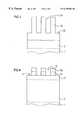
- FIG. 1is a fragmentary, diagrammatic, sectional view perpendicular to a surface of a first substrate with a doped region above which three layers of semiconductor material are disposed, with a first SiO 2 layer applied above them;
- FIG. 2is a fragmentary, sectional view according to FIG. 1 after the production of first trenches
- FIG. 3is a fragmentary, sectional view taken along the line III—III of FIG. 2, in the direction of the arrows, along a first trench after the formation of a second SiO 2 layer which fills the first trenches, and after the etching of SiO 2 for the purpose of producing second trenches, wherein this section retains its appearance even after process steps relating to FIGS. 5 and 6;
- FIG. 4is a fragmentary, sectional view taken along the line IV—IV of FIG. 2, in the direction of the arrows;
- FIG. 5is a fragmentary, sectional view showing the section of FIG. 4 after the etching of semiconductor material which concludes the formation of the second trenches, and after the production of a first insulation structure;
- FIG. 6is a fragmentary, sectional view showing the section of FIG. 5 after the second trenches have been filled with semiconductor material up to a first level and after the removal of parts of the first insulation structure, thereby producing capacitor dielectrics;
- FIG. 7is a fragmentary, sectional view showing the section of FIG. 6 after the production of second source/drain regions, gate oxides, word lines and gate electrodes;
- FIG. 8is a fragmentary, sectional view showing the section of FIG. 7 after the production of bit lines.
- FIG. 9is a fragmentary, sectional view showing the section of FIG. 2 along a second trench after the production of the bit lines.
- a starting materialwhich is a substrate that is made, for example, of monocrystalline silicon which is doped in a region B of a first conductivity type.
- the region Bhas, for example, a p-type doping with a dopant concentration of approximately 3*10 16 cm ⁇ 3 .
- the region Bis provided with a first layer 1 which is doped by a second conductivity type, opposite to the first conductivity type having a dopant concentration of approximately 10 20 cm ⁇ 3 , with a second layer 2 , which is doped by the first conductivity type having a dopant concentration of approximately 3*10 17 cm ⁇ 3 , and with a third layer 3 , which is doped by the second conductivity type having a dopant concentration of approximately 10 21 cm ⁇ 3 .
- the first layer 1 , the second layer 2 and the third layer 3are produced by epitaxial growth, for example.
- the third layer 3forms a surface 4 of the substrate.
- the first layer 1has a thickness of approximately 9 ⁇ m
- the second layer 2has a thickness of approximately 1 ⁇ m
- the third layer 3has a thickness of approximately 200 nm.
- a first SiO 2 layer O 1 having a thickness of approximately 150 nmis deposited on the surface 4 , as is seen in FIG. 1, in a TEOS process.
- the first SiO 2 layer O 1is structured with the aid of a first non-illustrated photoresist mask, and parts of the surface 4 are uncovered in order to be able to produce first trenches G 1 .
- the first trenches G 1are etched selectively with respect to SiO 2 , as is seen in FIG. 2, in an anisotropic dry etching process. HBr, NF 3 , He and O 2 are suitable, for example, for an etching process in which silicon is attacked selectively with respect to SiO 2 .
- the first trenches G 1are produced with a depth of approximately 800 nm and reach down into the second layer 2 .
- the first trenches G 1have a strip-shaped cross-section parallel to the surface 4 and run substantially parallel over the entire cell array.
- the first trenches G 1are filled by depositing a second SiO 2 layer O 2 having a thickness of 150 nm, for example, in a TEOS process.
- the surface 4is covered by parts of the first SiO 2 layer O 1 and by parts of the second SiO 2 layer O 2 , that is to say by a total of 300 nm of SiO 2 .
- SiO 2is etched selectively with respect to silicon through the use of an isotropic dry etching, with the aid of a second photoresist mask down to a second depth T 2 , which lies above an interface between the first layer 1 and the second layer 2 and below an interface between the second layer 2 and the third layer 3 and is approximately 400 nm from the surface 4 .
- a second depth T 2which lies above an interface between the first layer 1 and the second layer 2 and below an interface between the second layer 2 and the third layer 3 and is approximately 400 nm from the surface 4 .
- parts of the surface 4which is not attacked due to the selectivity of the etching, are uncovered, as is seen in FIG. 4 .
- CHF 3 , CF 4 and/or Arare suitable for an etching process in which SiO 2 is attacked selectively with respect to silicon.
- siliconis subsequently etched selectively with respect to SiO 2 down to a first depth T 1 within the first layer 1 .
- the first depth T 1lies 10 ⁇ m, for example, below the surface 4 .
- the second trenches G 2 that have been producedrun e.g. perpendicularly to the first trenches G 1 .
- the second trenches G 2have a width of approximately 200 nm and a length of approximately 50 ⁇ m. A distance between the centers of neighboring second trenches G 2 is approximately 400 nm.
- the first trenches G 1which are partially filled with SiO 2 , and the second trenches G 2 cross at crossover regions K.
- the second trenches G 2have the second depth T 2 at the crossover regions K seen in FIG.
- the second trenches G 2have the first depth T 1 in regions ⁇ overscore (K) ⁇ located between the crossover regions K, as is seen in FIG. 5 .
- the second trenches G 2thus cut through the third layer 3 and the second layer 2 in the regions ⁇ overscore (K) ⁇ located between the crossover regions K.
- the second trenches G 2have a strip-shaped cross-section parallel to the surface 4 and run substantially parallel. Remaining parts of the third layer 3 which are bounded by the first trenches G 1 and the second trenches G 2 are suitable as first source/drain regions S/D 1 .
- a first insulation structure I 1is produced by thermal oxidation of those areas of semiconductor material which adjoin the second trenches G 2 , as is seen in see FIG. 5 .
- the second trenches G 2are subsequently filled by depositing semiconductor material which is doped by the second conductivity type with a dopant concentration of approximately 10 21 cm ⁇ 3 .
- the thickness of the applied semiconductor materialis approximately 200 nm.
- Siliconis subsequently etched selectively with respect to SiO 2 , in such a way that the second trenches G 2 are filled with semiconductor material up to a first level H 1 in the regions ⁇ overscore (K) ⁇ located between the crossover regions K.
- the first level H 1is situated above an interface between the first layer 1 and second layer 2 and below a second depth T 2 .
- the first level H 1lies approximately 600 nm below the surface 4 .
- Parts of the first insulation structure I 1 which are uncovered as a resultare removed by a wet etching process with HF. Remaining parts of the first insulation structure I 1 are suitable as capacitor dielectrics Kd, as is seen in FIG. 6 .
- the second trenches G 2are subsequently filled by depositing semiconductor material which is doped by the second conductivity type with a dopant concentration of approximately 10 21 cm ⁇ 3 .
- the thickness of the deposited semiconductor materialis approximately 200 nm.
- Siliconis subsequently etched selectively with respect to SiO 2 , in such a way that the second trenches G 2 are filled with semiconductor material up to a second level H 2 , which lies above the first level H 1 and below the second depth T 2 , in the regions ⁇ overscore (K) ⁇ located between the crossover regions K.
- the second level H 2lies approximately 100 nm above the first level H 1 .
- the semiconductor material up to the second level H 2 in the regions ⁇ overscore (K) ⁇ of the second trenches G 2 which are located between the crossover regions Kis suitable as storage nodes Sp. Accordingly, the storage nodes Sp reach from the second layer 2 as far as into the first layer 1 .
- Dopantdiffuses out of the storage nodes into the second layer 2 by using an RTP process. Resultant regions doped by the second conductivity type are suitable as second source/drain regions S/D 2 , which are seen in FIG. 7 .
- a gate oxide I 2is produced within the second trenches G 2 through the use of thermal oxidation, for example.
- Conductive materialwhich contains e.g. polysilicon and/or metal silicide, is subsequently deposited in order to fill the second trenches G 2 .
- the thickness of the deposited conductive materialis approximately 200 nm.
- the conductive materialis etched selectively with respect to SiO 2 , in such a way that the second trenches G 2 are filled with conductive material up to a third level H 3 , which lies above the interface between the second layer 2 and the third layer 3 and below the surface 4 , in the regions ⁇ overscore (K) ⁇ located between the crossover regions K, as is seen in FIG. 7 .
- the third level H 3lies approximately 150 nm below the surface 4 .
- the deposited conductive materialforms word lines Wl which are suitable as gate electrodes G in the regions ⁇ overscore (K) ⁇ located between the crossover regions K.
- the gate electrodes Gare thus produced in a self-aligned manner above the storage nodes Sp.
- the second trenches G 2are filled by depositing SiO 2 , in a TEOS process.
- the thickness of the deposited SiO 2is approximately 200 nm.
- SiO 2is subsequently etched selectively with respect to silicon until the surface 4 is uncovered.
- the first SiO 2 layer O 1 and the second SiO 2 layer O 2are completely removed by this step. Since only the first source/drain regions S/D 1 and insulating materials adjoin a section along the surface 4 , contacts to the first source/drain regions S/D 1 are thereby opened in a self-aligned manner.
- Bit lines Blare produced by depositing and structuring conductive material, with the aid of a third photoresist mask having a form which corresponds to that of the first photoresist mask.
- the bit lines Blare disposed in such a way that they overlap the first source/drain regions S/D 1 , as is seen in FIGS. 8 and 9.
- the conductive materialcontains e.g. polysilicon, metal silicide and/or tungsten.
- Each MOS transistorincludes a gate electrode G, which is part of a word line Wl, two first source/drain regions S/D 1 , which have been produced by structuring the third layer 3 and overlap a bit line Bl, two channel regions which run perpendicular to the surface 4 , are located within the second layer 2 and are each adjoined by a gate oxide, and two second source/drain regions S/D 2 , which have been produced by outdiffusion of dopant from a storage node Sp into the second layer 2 and are connected to the storage node Sp, as is seen in FIG. 8 .
- SiO 2 in the first trenches G 1insulates neighboring transistors from one another in the word line direction, as well as word lines Wl from bit lines Bl.
- the storage nodes Spare disposed underneath the gate electrodes G.
- first SiO 2 layer O 1it is possible to form a layer on the surface 4 including e.g. three partial layers, of which a middle partial layer having a thickness of approximately 80 nm contains silicon nitride.
- An upper partial layer made of SiO 2 and having a thickness of approximately 50 nmis produced in a TEOS process, for example. It is thus necessary to etch not only SiO 2 but also silicon nitride in each etching process which uncovers parts of the surface 4 . This alternative reduces the risk of excessively deep etching being effected during the opening of the contacts of the first source/drain regions S/D 1 , which would lead to a short circuit between word lines Wl and bit lines Bl seen in FIG. 9 .
Landscapes
- Engineering & Computer Science (AREA)
- Manufacturing & Machinery (AREA)
- Semiconductor Memories (AREA)
Abstract
Description
Claims (7)
Priority Applications (1)
| Application Number | Priority Date | Filing Date | Title |
|---|---|---|---|
| US09/851,051US6420228B1 (en) | 1997-05-02 | 2001-05-08 | Method for the production of a DRAM cell configuration |
Applications Claiming Priority (2)
| Application Number | Priority Date | Filing Date | Title |
|---|---|---|---|
| DE19718721 | 1997-05-02 | ||
| DE19718721ADE19718721C2 (en) | 1997-05-02 | 1997-05-02 | DRAM cell arrangement and method for its production |
Related Child Applications (1)
| Application Number | Title | Priority Date | Filing Date |
|---|---|---|---|
| US09/851,051DivisionUS6420228B1 (en) | 1997-05-02 | 2001-05-08 | Method for the production of a DRAM cell configuration |
Publications (1)
| Publication Number | Publication Date |
|---|---|
| US6255684B1true US6255684B1 (en) | 2001-07-03 |
Family
ID=7828530
Family Applications (2)
| Application Number | Title | Priority Date | Filing Date |
|---|---|---|---|
| US09/071,798Expired - LifetimeUS6255684B1 (en) | 1997-05-02 | 1998-05-04 | DRAM cell configuration and method for its production |
| US09/851,051Expired - LifetimeUS6420228B1 (en) | 1997-05-02 | 2001-05-08 | Method for the production of a DRAM cell configuration |
Family Applications After (1)
| Application Number | Title | Priority Date | Filing Date |
|---|---|---|---|
| US09/851,051Expired - LifetimeUS6420228B1 (en) | 1997-05-02 | 2001-05-08 | Method for the production of a DRAM cell configuration |
Country Status (6)
| Country | Link |
|---|---|
| US (2) | US6255684B1 (en) |
| EP (1) | EP0875937A3 (en) |
| JP (1) | JPH10313100A (en) |
| KR (1) | KR100509210B1 (en) |
| DE (1) | DE19718721C2 (en) |
| TW (1) | TW411622B (en) |
Cited By (12)
| Publication number | Priority date | Publication date | Assignee | Title |
|---|---|---|---|---|
| US20020127797A1 (en)* | 1999-08-31 | 2002-09-12 | Micron Technology, Inc. | Multiple oxide thicknesses for merged memory and logic applications |
| US6492221B1 (en)* | 1998-09-30 | 2002-12-10 | Infineon, Ag | DRAM cell arrangement |
| US20030022833A1 (en)* | 1998-05-12 | 2003-01-30 | Greenville Hospital | Use of anti-prolactin agents to treat proliferative conditions |
| US6580154B2 (en)* | 1999-08-31 | 2003-06-17 | Micron Technology, Inc. | Method and apparatus on (110) surfaces of silicon structures with conduction in the <110> direction |
| US20030117865A1 (en)* | 2001-12-19 | 2003-06-26 | Franz Hofmann | Layer arrangement, memory cell, memory cell arrangement and method for producing a layer arrangement |
| US6642575B1 (en)* | 1998-12-04 | 2003-11-04 | Kabushiki Kaisha Toshiba | MOS transistor with vertical columnar structure |
| US6724031B1 (en)* | 2003-01-13 | 2004-04-20 | International Business Machines Corporation | Method for preventing strap-to-strap punch through in vertical DRAMs |
| US20040094810A1 (en)* | 2002-11-14 | 2004-05-20 | Infineon Technologies North America Corp. | High density DRAM with reduced peripheral device area and method of manufacture |
| US20040135187A1 (en)* | 2002-12-11 | 2004-07-15 | Dietrich Bonart | Dynamic memory cell and method of manufacturing same |
| US20050001257A1 (en)* | 2003-02-14 | 2005-01-06 | Till Schloesser | Method of fabricating and architecture for vertical transistor cells and transistor-controlled memory cells |
| US20050253180A1 (en)* | 2001-05-29 | 2005-11-17 | Till Schlosser | DRAM cell arrangement with vertical MOS transistors |
| US20100118465A1 (en)* | 2004-08-27 | 2010-05-13 | University Of South Florida | Method of Manufacturing Silicon Topological Capacitors |
Families Citing this family (12)
| Publication number | Priority date | Publication date | Assignee | Title |
|---|---|---|---|---|
| DE10008814B4 (en)* | 2000-02-25 | 2006-06-29 | Mosel Vitelic Inc. | Separating bottom for use in braking and/or clamping device, has flexible supporting elements projected from outer surface, where supporting elements with center line of base body enclose angle of preset values |
| US6537870B1 (en)* | 2000-09-29 | 2003-03-25 | Infineon Technologies Ag | Method of forming an integrated circuit comprising a self aligned trench |
| DE10134101B4 (en)* | 2001-07-13 | 2006-03-23 | Infineon Technologies Ag | Integrated semiconductor memory and manufacturing process |
| DE10334113A1 (en)* | 2003-07-25 | 2005-03-03 | Infineon Technologies Ag | Arrangement of vertical memory cells for DRAMs in a semiconductor substrate has conductive connection to inner electrode of memory cell in trench through trench surroundings |
| DE102004026000A1 (en)* | 2003-07-25 | 2005-02-24 | Infineon Technologies Ag | Cell field for DRAMs comprises memory cells having lower source/drain regions with sections of trenched source/drain layer perforated by perforated trenches and word line trenches |
| US20050088895A1 (en)* | 2003-07-25 | 2005-04-28 | Infineon Technologies Ag | DRAM cell array having vertical memory cells and methods for fabricating a DRAM cell array and a DRAM |
| US7135731B2 (en)* | 2003-12-10 | 2006-11-14 | Nanya Technology Corp. | Vertical DRAM and fabrication method thereof |
| JP5623005B2 (en) | 2008-02-01 | 2014-11-12 | ピーエスフォー ルクスコ エスエイアールエルPS4 Luxco S.a.r.l. | Semiconductor device and manufacturing method thereof |
| US9117701B2 (en)* | 2011-05-06 | 2015-08-25 | Semiconductor Energy Laboratory Co., Ltd. | Semiconductor device |
| US8609492B2 (en) | 2011-07-27 | 2013-12-17 | Micron Technology, Inc. | Vertical memory cell |
| WO2019005218A1 (en)* | 2017-06-26 | 2019-01-03 | Micron Technology, Inc. | Apparatuses having body connection lines coupled with access devices |
| WO2025079920A1 (en)* | 2023-10-10 | 2025-04-17 | 한양대학교 산학협력단 | Three-dimensional random access memory having improved structure |
Citations (6)
| Publication number | Priority date | Publication date | Assignee | Title |
|---|---|---|---|---|
| US5376575A (en) | 1991-09-26 | 1994-12-27 | Hyundai Electronics Industries, Inc. | Method of making dynamic random access memory having a vertical transistor |
| US5477071A (en) | 1992-03-19 | 1995-12-19 | Kabushiki Kaisha Toshiba | MOS random access memory having array of trench type one-capacitor/one-transistor memory cells |
| US5519236A (en) | 1993-06-28 | 1996-05-21 | Kabushiki Kaisha Toshiba | Semiconductor memory device having surrounding gate transistor |
| US5909618A (en)* | 1997-07-08 | 1999-06-01 | Micron Technology, Inc. | Method of making memory cell with vertical transistor and buried word and body lines |
| US5994735A (en)* | 1993-05-12 | 1999-11-30 | Mitsubishi Denki Kabushiki Kaisha | Semiconductor device having a vertical surround gate metal-oxide semiconductor field effect transistor, and manufacturing method thereof |
| US6034389A (en)* | 1997-01-22 | 2000-03-07 | International Business Machines Corporation | Self-aligned diffused source vertical transistors with deep trench capacitors in a 4F-square memory cell array |
Family Cites Families (10)
| Publication number | Priority date | Publication date | Assignee | Title |
|---|---|---|---|---|
| US4824793A (en)* | 1984-09-27 | 1989-04-25 | Texas Instruments Incorporated | Method of making DRAM cell with trench capacitor |
| US4914739A (en)* | 1984-10-31 | 1990-04-03 | Texas Instruments, Incorporated | Structure for contacting devices in three dimensional circuitry |
| US4797373A (en)* | 1984-10-31 | 1989-01-10 | Texas Instruments Incorporated | Method of making dRAM cell with trench capacitor |
| JPH0824165B2 (en)* | 1985-11-22 | 1996-03-06 | テキサス インスツルメンツ インコ−ポレイテツド | Integrated circuit |
| JPS63211750A (en)* | 1987-02-27 | 1988-09-02 | Mitsubishi Electric Corp | semiconductor storage device |
| JPH01227468A (en)* | 1988-03-08 | 1989-09-11 | Oki Electric Ind Co Ltd | Semiconductor storage device |
| US5103276A (en)* | 1988-06-01 | 1992-04-07 | Texas Instruments Incorporated | High performance composed pillar dram cell |
| US5218218A (en)* | 1990-02-01 | 1993-06-08 | Mitsubishi Denki Kabushiki Kaisha | Semiconductor device and manufacturing method thereof |
| JP3311070B2 (en)* | 1993-03-15 | 2002-08-05 | 株式会社東芝 | Semiconductor device |
| DE19519160C1 (en)* | 1995-05-24 | 1996-09-12 | Siemens Ag | DRAM cell arrangement having packing density required for specified memory |
- 1997
- 1997-05-02DEDE19718721Apatent/DE19718721C2/ennot_activeExpired - Fee Related
- 1998
- 1998-04-02EPEP98106069Apatent/EP0875937A3/ennot_activeWithdrawn
- 1998-04-10TWTW087105435Apatent/TW411622B/enactive
- 1998-04-30JPJP10134226Apatent/JPH10313100A/enactivePending
- 1998-05-01KRKR1019980015755Apatent/KR100509210B1/ennot_activeExpired - Fee Related
- 1998-05-04USUS09/071,798patent/US6255684B1/ennot_activeExpired - Lifetime
- 2001
- 2001-05-08USUS09/851,051patent/US6420228B1/ennot_activeExpired - Lifetime
Patent Citations (6)
| Publication number | Priority date | Publication date | Assignee | Title |
|---|---|---|---|---|
| US5376575A (en) | 1991-09-26 | 1994-12-27 | Hyundai Electronics Industries, Inc. | Method of making dynamic random access memory having a vertical transistor |
| US5477071A (en) | 1992-03-19 | 1995-12-19 | Kabushiki Kaisha Toshiba | MOS random access memory having array of trench type one-capacitor/one-transistor memory cells |
| US5994735A (en)* | 1993-05-12 | 1999-11-30 | Mitsubishi Denki Kabushiki Kaisha | Semiconductor device having a vertical surround gate metal-oxide semiconductor field effect transistor, and manufacturing method thereof |
| US5519236A (en) | 1993-06-28 | 1996-05-21 | Kabushiki Kaisha Toshiba | Semiconductor memory device having surrounding gate transistor |
| US6034389A (en)* | 1997-01-22 | 2000-03-07 | International Business Machines Corporation | Self-aligned diffused source vertical transistors with deep trench capacitors in a 4F-square memory cell array |
| US5909618A (en)* | 1997-07-08 | 1999-06-01 | Micron Technology, Inc. | Method of making memory cell with vertical transistor and buried word and body lines |
Non-Patent Citations (1)
| Title |
|---|
| "A Deep Trenched Capacitor Technology for 4 Mbit DRAMs", Proc. Intern. Electronic Devices and Materials IEDM 85, p. 702. |
Cited By (33)
| Publication number | Priority date | Publication date | Assignee | Title |
|---|---|---|---|---|
| US20030022833A1 (en)* | 1998-05-12 | 2003-01-30 | Greenville Hospital | Use of anti-prolactin agents to treat proliferative conditions |
| US6492221B1 (en)* | 1998-09-30 | 2002-12-10 | Infineon, Ag | DRAM cell arrangement |
| US6642575B1 (en)* | 1998-12-04 | 2003-11-04 | Kabushiki Kaisha Toshiba | MOS transistor with vertical columnar structure |
| US7282400B2 (en) | 1999-08-31 | 2007-10-16 | Micron Technology, Inc. | Method and apparatus on (110) surfaces of silicon structures with conduction in the <110> direction |
| US20060244057A1 (en)* | 1999-08-31 | 2006-11-02 | Micron Technology, Inc. | Multiple oxide thicknesses for merged memory and logic applications |
| US7045880B2 (en)* | 1999-08-31 | 2006-05-16 | Micron Technology, Inc. | Method and apparatus on (110) surfaces of silicon structures with conduction in the <110> direction |
| US20020127884A1 (en)* | 1999-08-31 | 2002-09-12 | Micron Technology, Inc. | Multiple oxide thicknesses for merged memory and logic applications |
| US20030209782A1 (en)* | 1999-08-31 | 2003-11-13 | Micron Technology, Inc. | Method and apparatus on (110) surfaces of silicon structures with conduction in the <110> direction |
| US6960821B2 (en) | 1999-08-31 | 2005-11-01 | Micron Technology, Inc. | Method and apparatus on (110) surfaces of silicon structures with conduction in the <110> direction |
| US7271467B2 (en) | 1999-08-31 | 2007-09-18 | Micron Technology, Inc. | Multiple oxide thicknesses for merged memory and logic applications |
| US6580154B2 (en)* | 1999-08-31 | 2003-06-17 | Micron Technology, Inc. | Method and apparatus on (110) surfaces of silicon structures with conduction in the <110> direction |
| US6800927B2 (en) | 1999-08-31 | 2004-10-05 | Micron Technology, Inc. | Multiple oxide thicknesses for merged memory and logic applications |
| US20060141697A1 (en)* | 1999-08-31 | 2006-06-29 | Micron Technology, Inc. | Method and apparatus on (110) surfaces of silicon structures with conduction in the <110> direction |
| US20050023593A1 (en)* | 1999-08-31 | 2005-02-03 | Micron Technology, Inc. | Multiple oxide thicknesses for merged memory and logic applications |
| US20050026369A1 (en)* | 1999-08-31 | 2005-02-03 | Micron Technology, Inc. | Method and apparatus on (110) surfaces of silicon structures with conduction in the <110> direction |
| US6887749B2 (en) | 1999-08-31 | 2005-05-03 | Micron Technology, Inc. | Multiple oxide thicknesses for merged memory and logic applications |
| US20020127797A1 (en)* | 1999-08-31 | 2002-09-12 | Micron Technology, Inc. | Multiple oxide thicknesses for merged memory and logic applications |
| US7329916B2 (en)* | 2001-05-29 | 2008-02-12 | Infineon Technologies Ag | DRAM cell arrangement with vertical MOS transistors |
| US20050253180A1 (en)* | 2001-05-29 | 2005-11-17 | Till Schlosser | DRAM cell arrangement with vertical MOS transistors |
| US6900495B2 (en)* | 2001-12-19 | 2005-05-31 | Infineon Technologies Ag | Layer arrangement, memory cell, memory cell arrangement and method for producing a layer arrangement |
| US20030117865A1 (en)* | 2001-12-19 | 2003-06-26 | Franz Hofmann | Layer arrangement, memory cell, memory cell arrangement and method for producing a layer arrangement |
| US6909152B2 (en) | 2002-11-14 | 2005-06-21 | Infineon Technologies, Ag | High density DRAM with reduced peripheral device area and method of manufacture |
| US20050130352A1 (en)* | 2002-11-14 | 2005-06-16 | Infineon Technologies North America Corp. | High density DRAM with reduced peripheral device area and method of manufacture |
| US20040094810A1 (en)* | 2002-11-14 | 2004-05-20 | Infineon Technologies North America Corp. | High density DRAM with reduced peripheral device area and method of manufacture |
| US7163891B2 (en) | 2002-11-14 | 2007-01-16 | Infineon Technologies Ag | High density DRAM with reduced peripheral device area and method of manufacture |
| US20040135187A1 (en)* | 2002-12-11 | 2004-07-15 | Dietrich Bonart | Dynamic memory cell and method of manufacturing same |
| US20060102946A1 (en)* | 2002-12-11 | 2006-05-18 | Dietrich Bonart | Dynamic memory cell and method of manufacturing the same |
| US7015526B2 (en) | 2002-12-11 | 2006-03-21 | Infineon Technologies Ag | Dynamic memory cell and method of manufacturing same |
| US6724031B1 (en)* | 2003-01-13 | 2004-04-20 | International Business Machines Corporation | Method for preventing strap-to-strap punch through in vertical DRAMs |
| US7109544B2 (en)* | 2003-02-14 | 2006-09-19 | Infineon Technologies Ag | Architecture for vertical transistor cells and transistor-controlled memory cells |
| US20050001257A1 (en)* | 2003-02-14 | 2005-01-06 | Till Schloesser | Method of fabricating and architecture for vertical transistor cells and transistor-controlled memory cells |
| US20100118465A1 (en)* | 2004-08-27 | 2010-05-13 | University Of South Florida | Method of Manufacturing Silicon Topological Capacitors |
| US7829409B2 (en)* | 2004-08-27 | 2010-11-09 | University Of South Florida | Method of manufacturing silicon topological capacitors |
Also Published As
| Publication number | Publication date |
|---|---|
| US6420228B1 (en) | 2002-07-16 |
| JPH10313100A (en) | 1998-11-24 |
| KR100509210B1 (en) | 2006-02-28 |
| EP0875937A3 (en) | 2003-08-27 |
| EP0875937A2 (en) | 1998-11-04 |
| DE19718721C2 (en) | 1999-10-07 |
| DE19718721A1 (en) | 1998-11-12 |
| KR19980086702A (en) | 1998-12-05 |
| TW411622B (en) | 2000-11-11 |
Similar Documents
| Publication | Publication Date | Title |
|---|---|---|
| US6255684B1 (en) | DRAM cell configuration and method for its production | |
| US6204140B1 (en) | Dynamic random access memory | |
| US6184549B1 (en) | Trench storage dynamic random access memory cell with vertical transfer device | |
| US5574299A (en) | Semiconductor device having vertical conduction transistors and cylindrical cell gates | |
| KR100437551B1 (en) | DRAM (DRAM) cell and manufacturing method thereof | |
| US6331725B1 (en) | Integrated circuitry | |
| US5831301A (en) | Trench storage dram cell including a step transfer device | |
| US6426253B1 (en) | Method of forming a vertically oriented device in an integrated circuit | |
| KR100403066B1 (en) | Improved vertical mosfet | |
| US6008513A (en) | Dynamic random access memory (DRAM) cells with minimum active cell areas using sidewall-space bit lines | |
| US5290726A (en) | DRAM cells having stacked capacitors of fin structures and method of making thereof | |
| KR100325472B1 (en) | Manufacturing Method of DRAM Memory Cells | |
| US20070032033A1 (en) | Connecting structure and method for manufacturing the same | |
| US5156993A (en) | Fabricating a memory cell with an improved capacitor | |
| US6414347B1 (en) | Vertical MOSFET | |
| US6566202B2 (en) | Integrated circuit having at least two vertical MOS transistors and method for manufacturing same | |
| US6087692A (en) | DRAM cell configuration and method for its fabrication | |
| US6541810B2 (en) | Modified vertical MOSFET and methods of formation thereof | |
| US6037209A (en) | Method for producing a DRAM cellular arrangement | |
| KR100517219B1 (en) | Dram cell arrangement with dynamic gain memory cells, and method for the production thereof | |
| US6518613B2 (en) | Memory cell configuration with capacitor on opposite surface of substrate and method for fabricating the same | |
| KR930004985B1 (en) | Dram cell having a stacked capacitor and method of fabricating therefor | |
| US6608340B1 (en) | Substrate assembly having a depression suitable for an integrated circuit configuration and method for its fabrication | |
| JP2739983B2 (en) | Semiconductor memory device and method of manufacturing the same | |
| KR20000013402A (en) | Fabrication method of memory capacitor |
Legal Events
| Date | Code | Title | Description |
|---|---|---|---|
| AS | Assignment | Owner name:SIEMENS AKTIENGESELLSCHAFT, GERMANY Free format text:ASSIGNMENT OF ASSIGNORS INTEREST;ASSIGNORS:ROESNER, WOFGANG;RISCH, LOTHAR;HOFMANN, FRANZ;REEL/FRAME:010972/0433 Effective date:19980525 | |
| STCF | Information on status: patent grant | Free format text:PATENTED CASE | |
| FPAY | Fee payment | Year of fee payment:4 | |
| FPAY | Fee payment | Year of fee payment:8 | |
| AS | Assignment | Owner name:INFINEON TECHNOLOGIES AG,GERMANY Free format text:ASSIGNMENT OF ASSIGNORS INTEREST;ASSIGNOR:SIEMENS AKTIENGESELLSCHAFT;REEL/FRAME:024120/0505 Effective date:19990331 | |
| XAS | Not any more in us assignment database | Free format text:ASSIGNMENT OF ASSIGNORS INTEREST;ASSIGNOR:SIEMENS AKTIENGESELLSCHAFT;REEL/FRAME:023957/0508 | |
| AS | Assignment | Owner name:QIMONDA AG,GERMANY Free format text:ASSIGNMENT OF ASSIGNORS INTEREST;ASSIGNOR:INFINEON TECHNOLOGIES AG;REEL/FRAME:023963/0502 Effective date:20060425 | |
| FPAY | Fee payment | Year of fee payment:12 | |
| AS | Assignment | Owner name:INFINEON TECHNOLOGIES AG, GERMANY Free format text:ASSIGNMENT OF ASSIGNORS INTEREST;ASSIGNOR:QIMONDA AG;REEL/FRAME:035623/0001 Effective date:20141009 | |
| AS | Assignment | Owner name:POLARIS INNOVATIONS LIMITED, IRELAND Free format text:ASSIGNMENT OF ASSIGNORS INTEREST;ASSIGNOR:INFINEON TECHNOLOGIES AG;REEL/FRAME:036293/0932 Effective date:20150708 |