US6255668B1 - Thin film transistor with inclined eletrode side surfaces - Google Patents
Thin film transistor with inclined eletrode side surfacesDownload PDFInfo
- Publication number
- US6255668B1 US6255668B1US09/317,952US31795299AUS6255668B1US 6255668 B1US6255668 B1US 6255668B1US 31795299 AUS31795299 AUS 31795299AUS 6255668 B1US6255668 B1US 6255668B1
- Authority
- US
- United States
- Prior art keywords
- conductive material
- semiconductor layer
- film transistor
- thin film
- gate electrode
- Prior art date
- Legal status (The legal status is an assumption and is not a legal conclusion. Google has not performed a legal analysis and makes no representation as to the accuracy of the status listed.)
- Expired - Lifetime
Links
Images


Classifications
- H—ELECTRICITY
- H10—SEMICONDUCTOR DEVICES; ELECTRIC SOLID-STATE DEVICES NOT OTHERWISE PROVIDED FOR
- H10D—INORGANIC ELECTRIC SEMICONDUCTOR DEVICES
- H10D30/00—Field-effect transistors [FET]
- H10D30/60—Insulated-gate field-effect transistors [IGFET]
- H10D30/67—Thin-film transistors [TFT]
- H—ELECTRICITY
- H10—SEMICONDUCTOR DEVICES; ELECTRIC SOLID-STATE DEVICES NOT OTHERWISE PROVIDED FOR
- H10D—INORGANIC ELECTRIC SEMICONDUCTOR DEVICES
- H10D30/00—Field-effect transistors [FET]
- H10D30/01—Manufacture or treatment
- H10D30/021—Manufacture or treatment of FETs having insulated gates [IGFET]
- H10D30/031—Manufacture or treatment of FETs having insulated gates [IGFET] of thin-film transistors [TFT]
- H10D30/0312—Manufacture or treatment of FETs having insulated gates [IGFET] of thin-film transistors [TFT] characterised by the gate electrodes
- H10D30/0316—Manufacture or treatment of FETs having insulated gates [IGFET] of thin-film transistors [TFT] characterised by the gate electrodes of lateral bottom-gate TFTs comprising only a single gate
- H—ELECTRICITY
- H10—SEMICONDUCTOR DEVICES; ELECTRIC SOLID-STATE DEVICES NOT OTHERWISE PROVIDED FOR
- H10D—INORGANIC ELECTRIC SEMICONDUCTOR DEVICES
- H10D30/00—Field-effect transistors [FET]
- H10D30/01—Manufacture or treatment
- H10D30/021—Manufacture or treatment of FETs having insulated gates [IGFET]
- H10D30/031—Manufacture or treatment of FETs having insulated gates [IGFET] of thin-film transistors [TFT]
- H10D30/0321—Manufacture or treatment of FETs having insulated gates [IGFET] of thin-film transistors [TFT] comprising silicon, e.g. amorphous silicon or polysilicon
- H—ELECTRICITY
- H10—SEMICONDUCTOR DEVICES; ELECTRIC SOLID-STATE DEVICES NOT OTHERWISE PROVIDED FOR
- H10D—INORGANIC ELECTRIC SEMICONDUCTOR DEVICES
- H10D30/00—Field-effect transistors [FET]
- H10D30/60—Insulated-gate field-effect transistors [IGFET]
- H10D30/67—Thin-film transistors [TFT]
- H10D30/6704—Thin-film transistors [TFT] having supplementary regions or layers in the thin films or in the insulated bulk substrates for controlling properties of the device
- H10D30/6713—Thin-film transistors [TFT] having supplementary regions or layers in the thin films or in the insulated bulk substrates for controlling properties of the device characterised by the properties of the source or drain regions, e.g. compositions or sectional shapes
- H—ELECTRICITY
- H10—SEMICONDUCTOR DEVICES; ELECTRIC SOLID-STATE DEVICES NOT OTHERWISE PROVIDED FOR
- H10D—INORGANIC ELECTRIC SEMICONDUCTOR DEVICES
- H10D30/00—Field-effect transistors [FET]
- H10D30/60—Insulated-gate field-effect transistors [IGFET]
- H10D30/67—Thin-film transistors [TFT]
- H10D30/6729—Thin-film transistors [TFT] characterised by the electrodes
- Y—GENERAL TAGGING OF NEW TECHNOLOGICAL DEVELOPMENTS; GENERAL TAGGING OF CROSS-SECTIONAL TECHNOLOGIES SPANNING OVER SEVERAL SECTIONS OF THE IPC; TECHNICAL SUBJECTS COVERED BY FORMER USPC CROSS-REFERENCE ART COLLECTIONS [XRACs] AND DIGESTS
- Y10—TECHNICAL SUBJECTS COVERED BY FORMER USPC
- Y10S—TECHNICAL SUBJECTS COVERED BY FORMER USPC CROSS-REFERENCE ART COLLECTIONS [XRACs] AND DIGESTS
- Y10S438/00—Semiconductor device manufacturing: process
- Y10S438/978—Semiconductor device manufacturing: process forming tapered edges on substrate or adjacent layers
Definitions
- the present inventionrelates to a semiconductor device, and in particular, to a thin film transistor and a method of fabricating the thin film transistor.
- Thin film transistorsserve as switching devices switching image data signals in each pixel region.
- Thin film transistorscan be used instead of CMOS load transistors or load resistors of a static random access memory (SRAM) of more than 1M bit.
- a liquid crystal display (LCD)includes an upper glass, a lower glass, and a liquid crystal interposed between the upper and lower glasses.
- the upper glasshas a black matrix layer, a common electrode, and R, G and B color filter layers.
- the lower glasshas data lines and gate line; crossing each other and pixel regions arranged in matrix.
- a pixel electrodeis formed in each pixel region, and an amorphous thin film transistor acting like an analog switch is formed to control charge stored in its capacitor.
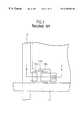
- FIG. 1is a lay-out of a related art liquid crystal display.
- the lower glassincludes a plurality of scanning lines 11 formed extending in one direction, a gate electrode 11 a extending from each scanning line 11 and data lines 12 crossing the scanning lines 11 .
- a thin film transistorincludes a source electrode 12 a and a drain electrode 12 b extending from the data lines 12 .
- Black matrix layersare arranged on the upper glass like a gauze to shut out the light in a region except the pixel electrodes (not shown) formed on the lower glass.
- R, G and B color filter layersare formed between the black matrix layers.
- a common electrodeis formed over the color filter layers and black matrix layers.
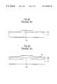
- a related art thin film transistorincludes a gate electrode 11 a formed on an insulating substrate 21 , a gate insulating layer 22 disposed on gate electrode 11 a and an amorphous silicon layer 23 disposed on gate insulating layer 22 to enclose the gate electrode 11 a .
- An n+ silicon layeris formed as an ohmic layer 24 to expose a part of the amorphous silicon layer 23 on the gate electrode 11 a , and the source electrode 12 a and the drain electrode 12 b are formed on the ohmic layer 24 .
- the material of each of the source and drain electrodes 12 a and 12 bis molybdenum.
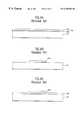
- the gate electrode 11 ais formed on a predetermined area of the insulating substrate 21 .
- An insulating layersuch as siliconitride SiN is formed on the substrate 21 including the gate electrode 11 a to form the gate insulating layer 22 .
- the insulating material used as the gate insulating layer 22serves as a capacitor dielectric in a storage capacitor area.
- an amorphous silicon layer 32 and an n+ silicon layer 33are formed on the gate insulating layer 22 .
- the n+ silicon layer 33 and the amorphous silicon layer 32are selectively removed to enclose the gate electrode 11 a .
- Molybdenum (Mo)is applied all over substrate 21 including the n+ silicon layer 33 as source and drain electrodes.
- the molybdenum material forming the source and drain electrodes and the n+ silicon layer 33are serially etched to expose the amorphous silicon layer 32 corresponding to a channel region and form the source and drain electrodes 12 a and 12 b .
- Molybdenum (not shown), the material forming the source and drain electrodes,is patterned on the gate insulating layer 22 in the storage capacitor area of the pixel region to contact a pixel electrode in the post manufacturing process.
- a passivation layer 34is formed all over the substrate 21 including the source and drain electrodes 12 a and 12 b .
- the manufacture of the thin film transistoris complete.
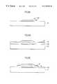
- FIGS. 4A to 4 Jdepict the steps in the manufacture of the second related art thin film transistor.
- a gate material 44 formed of chromium 42 and molybdenum 43is formed on a predetermined area of substrate 41 .
- the gate material 44can be constituted by either two layers (e.g., chromium 42 and molybdenum 43 ) or one layer.
- the gate material 44is patterned to form a gate electrode 44 a by a general patterning process. Sides of the gate electrode 44 a have a slant when formed by a reactive ion etching A) when patterning the two-layered gate electrode 44 a formed by molybdenum 43 and chromium 42 .
- a gate insulating layer 45is deposited all over the gate electrode 44 a and the substrate 41 .
- the gate electrode 44 ais inclined at its edge to improve the coverage in the corresponding area.
- a gate electrode having a slant at its edge and a technique of improving the coverageare disclosed in U.S. Pat. No. 5,132,745.
- an amorphous silicon layer 46is serially deposited on the gate insulating layer 45 in a vacuum chamber.
- An n+ amorphous silicon layer 47is serially deposited on the amorphous silicon layer 46 .
- the n+ amorphous silicon layer 47 and the amorphous silicon layer 46are selectively removed except in an area where a thin film transistor is formed on the substrate 41 .
- a first conductive layer 48is deposited to a thickness of 0.01 to 0.1 ⁇ m on the gate insulating layer 45 including the patterned n+ amorphous silicon layer 47 and the amorphous silicon layer 46 .
- the first conductive layer 48is made of chromium (Cr) in ohmic contact with the n+ amorphous silicon layer 47 .
- the first conductive layer 48can be made of a material such as nichromium (nickel and chrormium) and tantalum.
- a second conductive layer 49is deposited to a thickness of 0.1 to 1 ⁇ m on the first conductive layer 48 .
- the second conductive layer 49is made of molybdenum, and may be made of aluminum or tungsten.
- the use of molybdenum as second conductive layer 49assures better conductivity than that of source and drain electrodes made of chromium (Cr), which constitutes the first conductive layer 48 .
- Molybdenumassures a good ohmic contact for source and drain electrodes and the n+ amorphous silicon layer 47 .
- a photoresist 50is applied on the second conductive material 49 .
- the photoresist 50 corresponding to the channel region of the thin film transistoris removed, and the photoresist 50 is patterned to have edges slanted by 45°.
- the second conductive material 49is etched using the photoresist 50 as a mask with a requirement that the first conductive layer 48 is not effected.
- SF 6 gas of 37.5 sccm, Cl 2 gas of 6.5 sccm, and O 2 gas of 16 sccmare used and a pressure of 6.5 mTorr is maintained.
- the etching processis carried out under Rf plasma. Since the photoresist 50 is patterned with inclined edges, the second conductive material 49 also becomes patterned with inclined edges.
- the exposed first conductive layer 48 , Cris selectively etched by changing the requirements for etching the second conductive layer 49 .
- the first conductive layer 48is etched in a different process than the second conductive layer 49 .
- Etching the first conductive layer 48forms a source electrode 51 and a drain electrode 51 a , which are respectively made of the first conductive layer 48 and second conductive layer 49 .
- the first conductive layer 48is etched away by the use of chroline gas, Cl 2 gas of 70 sccm and O 2 gas of 30 sccm as a source gas under the pressure of 100 mTorr.
- the first conductive material 48 and the photoresistare in the etching ratio of 1 to 1.
- the first conductive layer 48 , Cris used as an etch stopper of the second conductive layer 49 , and the etching speed of molybdenum, the second conductive layer 49 is higher than that of first conductive layer 48 , Cr.
- molybdenum and chromiumare inclined at their respective edges. As shown in FIG.
- the exposed n+ amorphous silicon layer 47is etched to expose a part of the amorphous silicon layer 46 . Further, after removing the photoresist, a the passivation layer 60 is formed all over the substrate 41 including the source electrode 51 and the drain electrode 51 a , to complete the manufacture of the second related art thin film transistor.
- the related art method of manufacturing the thin film transistorhas various problems.
- a two-step etching processis needed that increases the time to perform the etching process.
- the etching gas for etching the molybdenumetches the n+ amorphous silicon through the holes.
- An object of the present inventionis to provide a thin film transistor and method of fabricating a thin film transistor that substantially obviates one or more of the problems caused by limitations and disadvantages of the related art.
- Another object of the present inventionis to provide a thin film transistor and method of manufacturing the same that has source and drain electrodes formed by a single etching process.
- Another object of the present inventionis to provide a thin film transistor and method of manufacturing the same that has a less complex manufacturing process.
- the present inventionincludes a thin film transistor that includes a thin film transistor including a substrate; a gate on the substrate; a gate insulating layer on the substrate and the gate electrode; a first semiconductor layer on the gate insulating layer; a second semiconductor layer on the first semiconductor layer; and first and second electrodes on the second semiconductor layer to expose the second semiconductor layer over the gate, wherein edges of the first and second electrodes adjacent to the exposed surface of the second semiconductor layer are non-linearly inclined.
- a thin film transistorincludes a thin film transistor including a substrate; a gate electrode on the substrate; a gate insulating layer on the substrate and the gate electrode; a first semiconductor layer on the gate insulating layer; a second semiconductor layer on the first semiconductor layer on the gate electrode; a first conductive material on the second semiconductor layer; and a second conductive material on the first conductive material, to expose edges of the first conductive material.
- a method of fabricating a thin film transistor according to the present inventionincludes forming a trapezoidal shaped gate electrode on a substrate; forming a gate insulating layer on the substrate and the gate electrode; forming a first semiconductor layer on the gate insulating layer; forming a second semiconductor layer on the first semiconductor layer; depositing a first conductive material and a second conductive material on the second semiconductor layer; and selectively removing the first conductive material and the second conductive material using a single etching gas to expose a prescribed part of the second semiconductor layer over the gate electrode, wherein respective edges of the etched first and second conductive materials are non-linearly inclined.
- FIG. 1is a diagram showing a related art liquid crystal display
- FIG. 2is a diagram showing a sectional view along line of I-I′ of FIG. 1;
- FIGS. 3A to 3 Dare diagrams showing sectional views of a related art thin film transistor
- FIGS. 4A to 4 Jare diagrams showing sectional views of steps in the manufacture of a related art thin film transistor
- FIG. 5is a diagram showing a sectional view of a preferred embodiment of a thin film transistor in accordance with the present invention.
- FIGS. 6A to 6 Hare diagrams showing cross-sectional views of a preferred embodiment of a method to manufacture a thin film transistor in accordance with the present invention.
- FIG. 5is a diagram showing a cross-section of a preferred embodiment of a thin film transistor in accordance with the present invention.
- the preferred embodiment of the thin film transistorincludes a substrate 61 , a gate electrode 64 formed on the substrate 61 , a gate insulating layer 65 formed all over substrate 61 including the gate electrode 64 and an amorphous silicon layer 66 formed on the gate insulating layer 65 .
- the gate electrode 64preferably has a trapezoidal cross-section.
- An n+ amorphous silicon layer 67is separately formed on the amorphous silicon layer 66 to expose the amorphous silicon layer 66 , which is used as a channel region.
- Source and drain electrodes 71 and 71 bare formed on the n+ amorphous silicon layer 67 and preferably have a non-linear slant or step at their edges.
- a passivation layer 72is formed on the substrate 61 including the source and drain electrodes 71 a and 71 b .
- the source and drain electrodes 71 a and 71 bare preferably made of two-layered conductive material.
- a first conductive materialis preferably chromium (Cr) and a second conductive material is preferably molybdenum. As shown in FIG. 5, an edge of the first conductive material (Cr) adjacent to the channel region does not correspond to an edge of the second conductive material (Mo).
- TFTthin film transistor
- a chromium (Cr) layer 62is formed on an insulating substrate 61 as a gate electrode material, and a molybdenum layer 63 is formed on the chromium layer 62 .
- the gate electrode materialis selectively removed by an etching technique to form the gate electrode 64 .
- the gate electrode 64is preferably made of chromium and molybdenum.
- the gate electrode 64can be made, for example, of molybdenum only.
- the gate electrodepreferably has a trapezoidal crosssection.
- a gate insulating layer 65is formed all over the substrate 61 including the gate electrode 64 .
- An amorphous silicon layer 66is deposited on the gate insulating layer 65 in a vacuum chamber used for the deposition of gate insulating layer 65 .
- An n+ amorphous silicon layer 67is serially deposited on the amorphous silicon layer 66 .
- the n+ amorphous silicon layer 67 and the amorphous silicon layer 66 on the substrate 61are selectively removed except for a thin film transistor area.
- a first conductive material 68is deposited on the gate insulating layer 65 including the patterned n+ amorphous silicon layer 67 , and the amorphous silicon layer 66 to be used as a source and a drain electrode material.
- Chromiumis preferably used for the first conductive material 68 .
- the first conductive material 68may be nichromium (alloy of nickel and chromium) or tantalum having a good ohmic contact with the n+ amorphous silicon layer 67 .
- a second conductive material 69is deposited on the first conductive material 68 to be relatively thicker than the first conductive material 68 .
- the second conductive material 69is preferably molybdenum, but can be aluminum or tungsten.
- photoresist 70is applied to the second conductive material 69 .
- the photoresist 70is removed on the channel region of the thin film transistor by photolithography.
- the second conductive material 69 and the first conductive material 68are serially etched by the same etching gas in a single process using the patterned photoresist 70 as a mask.
- Cl 2 gas+O 2 gasare preferably used as the etching gas, and the amount of Cl 2 gas is approximately in the range of 400 to 600 sccm and more preferably, 500 sccm.
- the amount of O 2 gasis approximately in the range of 300 to 500 sccm, and more preferably, 400 sccm.
- the pressure during etchingis approximately in the range of 100 to 200 mTorr, and RF power is approximately 0.5 to 0.8 watts/cm 2 , and more preferably, 0.66 watts/cm 2 .
- Reactive ion etching or plasma etchingcan be used.
- the first conductive material 68 and the second conductive material 69are serially etched in the same chamber without changing the etching condition to pattern the source and drain electrodes 71 a and 71 b.
- chromium, the first conductive material 68 and molybdenum, the second conductive material 69have different etching ratios. Accordingly, edges of the source and drain electrodes are in steps or tiers. Chromium and molybdenum reacting to the Cl 2 +O 2 etching gas, have an etching ratio of 10 to 1. Further, chromium, the first conductive material 68 , and the n+ amorphous silicon layer 67 have an etching ratio of 4 to 1.
- the n+ amorphous silicon layer 67is not over-etched even if holes area formed by particles when depositing the first conductive material 68 .
- the etching selection ratio of the gate insulating layer 65 in the pixel area adjacent to the edge of drain electrode 71 bcan be secured to prevent the gate insulating layer 65 from being over-etched.
- the exposed n+ amorphous silicon layer 67is etched to expose the amorphous silicon layer 66 .
- the photoresist 70is removed.
- passivation layer 72is formed all over substrate 61 including the source and drain electrodes 71 a and 71 b to complete the preferred embodiment of a method for manufacturing a thin film transistor according to the present invention.
- the preferred embodiments of a thin film transistor and a manufacturing method for the samehave various advantages.
- the preferred embodimentsemploy a single etching process in patterning the two-layered source and drain electrodes to simplify the production process, reduce the process steps (e.g., separate etching steps) and reduce manufacturing costs. Further, the preferred embodiments improve step coverage at the edge of the drain electrode toward the storage capacitor to increase the reliability of semiconductor devices.
- a nail and a screwmay not be structural equivalents in that a nail employs a cylindrical surface to secure wooden parts together, whereas a screw employs a helical surface, in the environment of fastening wooden parts, a nail and a screw may be equivalent structures.
Landscapes
- Thin Film Transistor (AREA)
- Electrodes Of Semiconductors (AREA)
- Drying Of Semiconductors (AREA)
Abstract
Description
Claims (11)
Priority Applications (1)
| Application Number | Priority Date | Filing Date | Title |
|---|---|---|---|
| US09/810,232US6455357B2 (en) | 1998-06-05 | 2001-03-19 | Thin film transistor and method of fabricating the same |
Applications Claiming Priority (2)
| Application Number | Priority Date | Filing Date | Title |
|---|---|---|---|
| KR1019980020848AKR100301803B1 (en) | 1998-06-05 | 1998-06-05 | Thin film transistor and its manufacturing method |
| KR98-20848 | 1998-06-05 |
Related Child Applications (1)
| Application Number | Title | Priority Date | Filing Date |
|---|---|---|---|
| US09/810,232DivisionUS6455357B2 (en) | 1998-06-05 | 2001-03-19 | Thin film transistor and method of fabricating the same |
Publications (1)
| Publication Number | Publication Date |
|---|---|
| US6255668B1true US6255668B1 (en) | 2001-07-03 |
Family
ID=19538443
Family Applications (2)
| Application Number | Title | Priority Date | Filing Date |
|---|---|---|---|
| US09/317,952Expired - LifetimeUS6255668B1 (en) | 1998-06-05 | 1999-05-25 | Thin film transistor with inclined eletrode side surfaces |
| US09/810,232Expired - Fee RelatedUS6455357B2 (en) | 1998-06-05 | 2001-03-19 | Thin film transistor and method of fabricating the same |
Family Applications After (1)
| Application Number | Title | Priority Date | Filing Date |
|---|---|---|---|
| US09/810,232Expired - Fee RelatedUS6455357B2 (en) | 1998-06-05 | 2001-03-19 | Thin film transistor and method of fabricating the same |
Country Status (5)
| Country | Link |
|---|---|
| US (2) | US6255668B1 (en) |
| JP (1) | JP3133987B2 (en) |
| KR (1) | KR100301803B1 (en) |
| DE (1) | DE19916073B4 (en) |
| TW (1) | TW571443B (en) |
Cited By (18)
| Publication number | Priority date | Publication date | Assignee | Title |
|---|---|---|---|---|
| US6337284B1 (en)* | 1999-05-27 | 2002-01-08 | Lg. Philips Lcd Co., Ltd. | Liquid crystal display device and method of manufacturing the same |
| US6387737B1 (en)* | 2000-03-08 | 2002-05-14 | Semiconductor Energy Laboratory Co., Ltd. | Semiconductor device and manufacturing method thereof |
| US6455357B2 (en)* | 1998-06-05 | 2002-09-24 | Hyundai Electronics Industries Co., Ltd. | Thin film transistor and method of fabricating the same |
| US20020171085A1 (en)* | 2001-03-06 | 2002-11-21 | Hideomi Suzawa | Semiconductor device and manufacturing method thereof |
| US6573564B2 (en)* | 1997-09-29 | 2003-06-03 | Semiconductor Energy Laboratory Co., Ltd. | Semiconductor device and fabrication method thereof |
| US6709901B1 (en) | 2000-03-13 | 2004-03-23 | Semiconductor Energy Laboratory Co., Ltd. | Semiconductor device having stick drivers and a method of manufacturing the same |
| US6762082B2 (en) | 2000-03-06 | 2004-07-13 | Semiconductor Energy Laboratory Co., Ltd. | Semiconductor device and method of fabricating the same |
| US6855957B1 (en) | 2000-03-13 | 2005-02-15 | Semiconductor Energy Laboratory Co., Ltd. | Semiconductor device and manufacturing method thereof |
| US6900084B1 (en) | 2000-05-09 | 2005-05-31 | Semiconductor Energy Laboratory Co., Ltd. | Semiconductor device having a display device |
| US7102718B1 (en) | 2000-03-16 | 2006-09-05 | Semiconductor Energy Laboratory Co., Ltd. | Liquid crystal display device with particular TFT structure and method of manufacturing the same |
| US20070146568A1 (en)* | 2000-03-17 | 2007-06-28 | Semiconductor Energy Laboratory Co., Ltd. | Liquid crystal display device and manufacturing method thereof |
| US20100295048A1 (en)* | 2009-05-19 | 2010-11-25 | Te-Chen Chung | TFT Array Substrate and Method for Forming the Same |
| US9397194B2 (en) | 2008-09-01 | 2016-07-19 | Semiconductor Energy Laboratory Co., Ltd. | Method for manufacturing semiconductor device with oxide semiconductor ohmic conatct layers |
| US10205030B2 (en) | 2008-08-08 | 2019-02-12 | Semiconductor Energy Laboratory Co., Ltd. | Method for manufacturing semiconductor device |
| US10937897B2 (en) | 2008-07-31 | 2021-03-02 | Semiconductor Energy Laboratory Co., Ltd. | Semiconductor device and method for manufacturing the same |
| JP2021103784A (en)* | 2009-02-25 | 2021-07-15 | 株式会社半導体エネルギー研究所 | Display device |
| US20230111213A1 (en)* | 2021-10-07 | 2023-04-13 | Changhoon Jeon | Vacuum tunneling device and method of manufacturing the same |
| US12068329B2 (en) | 2008-07-31 | 2024-08-20 | Semiconductor Energy Laboratory Co., Ltd. | Semiconductor device and method for manufacturing the same |
Families Citing this family (42)
| Publication number | Priority date | Publication date | Assignee | Title |
|---|---|---|---|---|
| US6413949B1 (en) | 1995-06-07 | 2002-07-02 | D-Pharm, Ltd. | Prodrugs with enhanced penetration into cells |
| US7550794B2 (en) | 2002-09-20 | 2009-06-23 | Idc, Llc | Micromechanical systems device comprising a displaceable electrode and a charge-trapping layer |
| US6313106B1 (en) | 1995-06-07 | 2001-11-06 | D-Pharm Ltd. | Phospholipid derivatives of valproic acid and mixtures thereof |
| TW480554B (en)* | 1999-07-22 | 2002-03-21 | Semiconductor Energy Lab | Semiconductor device and manufacturing method thereof |
| JP4630420B2 (en)* | 2000-05-23 | 2011-02-09 | ティーピーオー ホンコン ホールディング リミテッド | Pattern formation method |
| US6794119B2 (en) | 2002-02-12 | 2004-09-21 | Iridigm Display Corporation | Method for fabricating a structure for a microelectromechanical systems (MEMS) device |
| EP2246726B1 (en) | 2004-07-29 | 2013-04-03 | QUALCOMM MEMS Technologies, Inc. | System and method for micro-electromechanical operating of an interferometric modulator |
| US7373026B2 (en)* | 2004-09-27 | 2008-05-13 | Idc, Llc | MEMS device fabricated on a pre-patterned substrate |
| US7327510B2 (en)* | 2004-09-27 | 2008-02-05 | Idc, Llc | Process for modifying offset voltage characteristics of an interferometric modulator |
| US7369296B2 (en) | 2004-09-27 | 2008-05-06 | Idc, Llc | Device and method for modifying actuation voltage thresholds of a deformable membrane in an interferometric modulator |
| US7417783B2 (en) | 2004-09-27 | 2008-08-26 | Idc, Llc | Mirror and mirror layer for optical modulator and method |
| US8003449B2 (en)* | 2004-11-26 | 2011-08-23 | Semiconductor Energy Laboratory Co., Ltd. | Method of manufacturing a semiconductor device having a reverse staggered thin film transistor |
| TW200628877A (en) | 2005-02-04 | 2006-08-16 | Prime View Int Co Ltd | Method of manufacturing optical interference type color display |
| CA2616268A1 (en) | 2005-07-22 | 2007-02-01 | Qualcomm Incorporated | Mems devices having support structures and methods of fabricating the same |
| EP2495212A3 (en) | 2005-07-22 | 2012-10-31 | QUALCOMM MEMS Technologies, Inc. | Mems devices having support structures and methods of fabricating the same |
| US7580172B2 (en) | 2005-09-30 | 2009-08-25 | Qualcomm Mems Technologies, Inc. | MEMS device and interconnects for same |
| US7630114B2 (en) | 2005-10-28 | 2009-12-08 | Idc, Llc | Diffusion barrier layer for MEMS devices |
| US7382515B2 (en) | 2006-01-18 | 2008-06-03 | Qualcomm Mems Technologies, Inc. | Silicon-rich silicon nitrides as etch stops in MEMS manufacture |
| US7652814B2 (en) | 2006-01-27 | 2010-01-26 | Qualcomm Mems Technologies, Inc. | MEMS device with integrated optical element |
| US7450295B2 (en) | 2006-03-02 | 2008-11-11 | Qualcomm Mems Technologies, Inc. | Methods for producing MEMS with protective coatings using multi-component sacrificial layers |
| US7643203B2 (en) | 2006-04-10 | 2010-01-05 | Qualcomm Mems Technologies, Inc. | Interferometric optical display system with broadband characteristics |
| US7711239B2 (en) | 2006-04-19 | 2010-05-04 | Qualcomm Mems Technologies, Inc. | Microelectromechanical device and method utilizing nanoparticles |
| US7417784B2 (en) | 2006-04-19 | 2008-08-26 | Qualcomm Mems Technologies, Inc. | Microelectromechanical device and method utilizing a porous surface |
| US7623287B2 (en) | 2006-04-19 | 2009-11-24 | Qualcomm Mems Technologies, Inc. | Non-planar surface structures and process for microelectromechanical systems |
| US7369292B2 (en) | 2006-05-03 | 2008-05-06 | Qualcomm Mems Technologies, Inc. | Electrode and interconnect materials for MEMS devices |
| US7405863B2 (en) | 2006-06-01 | 2008-07-29 | Qualcomm Mems Technologies, Inc. | Patterning of mechanical layer in MEMS to reduce stresses at supports |
| US7566664B2 (en) | 2006-08-02 | 2009-07-28 | Qualcomm Mems Technologies, Inc. | Selective etching of MEMS using gaseous halides and reactive co-etchants |
| US7545552B2 (en) | 2006-10-19 | 2009-06-09 | Qualcomm Mems Technologies, Inc. | Sacrificial spacer process and resultant structure for MEMS support structure |
| US7706042B2 (en) | 2006-12-20 | 2010-04-27 | Qualcomm Mems Technologies, Inc. | MEMS device and interconnects for same |
| US7535621B2 (en) | 2006-12-27 | 2009-05-19 | Qualcomm Mems Technologies, Inc. | Aluminum fluoride films for microelectromechanical system applications |
| US7733552B2 (en) | 2007-03-21 | 2010-06-08 | Qualcomm Mems Technologies, Inc | MEMS cavity-coating layers and methods |
| US7719752B2 (en) | 2007-05-11 | 2010-05-18 | Qualcomm Mems Technologies, Inc. | MEMS structures, methods of fabricating MEMS components on separate substrates and assembly of same |
| US7625825B2 (en) | 2007-06-14 | 2009-12-01 | Qualcomm Mems Technologies, Inc. | Method of patterning mechanical layer for MEMS structures |
| US8068268B2 (en) | 2007-07-03 | 2011-11-29 | Qualcomm Mems Technologies, Inc. | MEMS devices having improved uniformity and methods for making them |
| US7570415B2 (en) | 2007-08-07 | 2009-08-04 | Qualcomm Mems Technologies, Inc. | MEMS device and interconnects for same |
| KR101425131B1 (en)* | 2008-01-15 | 2014-07-31 | 삼성디스플레이 주식회사 | Display substrate and display device comprising the same |
| US7863079B2 (en) | 2008-02-05 | 2011-01-04 | Qualcomm Mems Technologies, Inc. | Methods of reducing CD loss in a microelectromechanical device |
| KR102244389B1 (en)* | 2010-01-22 | 2021-04-26 | 가부시키가이샤 한도오따이 에네루기 켄큐쇼 | Semiconductor device |
| KR101984218B1 (en)* | 2011-01-28 | 2019-05-30 | 가부시키가이샤 한도오따이 에네루기 켄큐쇼 | Method for manufacturing semiconductor device and semiconductor device |
| US8659816B2 (en) | 2011-04-25 | 2014-02-25 | Qualcomm Mems Technologies, Inc. | Mechanical layer and methods of making the same |
| KR20130139438A (en)* | 2012-06-05 | 2013-12-23 | 삼성디스플레이 주식회사 | Thin film transistor array panel |
| KR102039102B1 (en)* | 2012-12-24 | 2019-11-01 | 삼성디스플레이 주식회사 | Thin film transistor array panel and method of manufacturing the same |
Citations (1)
| Publication number | Priority date | Publication date | Assignee | Title |
|---|---|---|---|---|
| US5198694A (en) | 1990-10-05 | 1993-03-30 | General Electric Company | Thin film transistor structure with improved source/drain contacts |
Family Cites Families (9)
| Publication number | Priority date | Publication date | Assignee | Title |
|---|---|---|---|---|
| EP0236629B1 (en)* | 1986-03-06 | 1994-05-18 | Kabushiki Kaisha Toshiba | Driving circuit of a liquid crystal display device |
| US5320979A (en)* | 1987-07-20 | 1994-06-14 | Nippon Telegraph And Telephone Corporation | Method of connecting wirings through connection hole |
| JP2590938B2 (en)* | 1987-10-02 | 1997-03-19 | 旭硝子株式会社 | Thin film transistor substrate |
| JPH0224631A (en)* | 1988-07-13 | 1990-01-26 | Seikosha Co Ltd | Thin film transistor array |
| JPH04198923A (en)* | 1990-11-28 | 1992-07-20 | Mitsubishi Electric Corp | Display device manufacturing method |
| US5318667A (en)* | 1991-04-04 | 1994-06-07 | Hitachi, Ltd. | Method and apparatus for dry etching |
| US5273920A (en)* | 1992-09-02 | 1993-12-28 | General Electric Company | Method of fabricating a thin film transistor using hydrogen plasma treatment of the gate dielectric/semiconductor layer interface |
| US5650358A (en) | 1995-08-28 | 1997-07-22 | Ois Optical Imaging Systems, Inc. | Method of making a TFT having a reduced channel length |
| KR100301803B1 (en)* | 1998-06-05 | 2001-09-22 | 김영환 | Thin film transistor and its manufacturing method |
- 1998
- 1998-06-05KRKR1019980020848Apatent/KR100301803B1/ennot_activeExpired - Lifetime
- 1998-07-29TWTW087112416Apatent/TW571443B/ennot_activeIP Right Cessation
- 1998-12-17JPJP10358628Apatent/JP3133987B2/ennot_activeExpired - Fee Related
- 1999
- 1999-04-09DEDE19916073Apatent/DE19916073B4/ennot_activeExpired - Lifetime
- 1999-05-25USUS09/317,952patent/US6255668B1/ennot_activeExpired - Lifetime
- 2001
- 2001-03-19USUS09/810,232patent/US6455357B2/ennot_activeExpired - Fee Related
Patent Citations (2)
| Publication number | Priority date | Publication date | Assignee | Title |
|---|---|---|---|---|
| US5198694A (en) | 1990-10-05 | 1993-03-30 | General Electric Company | Thin film transistor structure with improved source/drain contacts |
| US5362660A (en) | 1990-10-05 | 1994-11-08 | General Electric Company | Method of making a thin film transistor structure with improved source/drain contacts |
Cited By (73)
| Publication number | Priority date | Publication date | Assignee | Title |
|---|---|---|---|---|
| US6573564B2 (en)* | 1997-09-29 | 2003-06-03 | Semiconductor Energy Laboratory Co., Ltd. | Semiconductor device and fabrication method thereof |
| US6455357B2 (en)* | 1998-06-05 | 2002-09-24 | Hyundai Electronics Industries Co., Ltd. | Thin film transistor and method of fabricating the same |
| USRE41632E1 (en)* | 1999-05-27 | 2010-09-07 | Lg Display Co., Ltd. | Liquid crystal display device and method of manufacturing the same |
| USRE40028E1 (en)* | 1999-05-27 | 2008-01-22 | Lg. Philips Lcd Co., Ltd. | Liquid crystal display device and method of manufacturing the same |
| US6337284B1 (en)* | 1999-05-27 | 2002-01-08 | Lg. Philips Lcd Co., Ltd. | Liquid crystal display device and method of manufacturing the same |
| US9099355B2 (en) | 2000-03-06 | 2015-08-04 | Semiconductor Energy Laboratory Co., Ltd. | Semiconductor device and method of fabricating the same |
| US7705354B2 (en) | 2000-03-06 | 2010-04-27 | Semiconductor Energy Laboratory Co., Ltd | Semiconductor device and method for fabricating the same |
| US7973312B2 (en) | 2000-03-06 | 2011-07-05 | Semiconductor Energy Laboratory Co., Ltd. | Semiconductor device and method of fabricating the same |
| US8188478B2 (en) | 2000-03-06 | 2012-05-29 | Semiconductor Energy Laboratory Co., Ltd. | Semiconductor device and method of fabricating the same |
| US6762082B2 (en) | 2000-03-06 | 2004-07-13 | Semiconductor Energy Laboratory Co., Ltd. | Semiconductor device and method of fabricating the same |
| US6806495B1 (en) | 2000-03-06 | 2004-10-19 | Semiconductor Energy Laboratory Co., Ltd. | Semiconductor device and method of fabricating the same |
| US9059045B2 (en) | 2000-03-08 | 2015-06-16 | Semiconductor Energy Laboratory Co., Ltd. | Semiconductor device and manufacturing method thereof |
| US7652294B2 (en) | 2000-03-08 | 2010-01-26 | Semiconductor Energy Laboratory Co., Ltd. | Semiconductor device and manufacturing method thereof |
| US9368514B2 (en) | 2000-03-08 | 2016-06-14 | Semiconductor Energy Laboratory Co., Ltd. | Semiconductor device and manufacturing method thereof |
| US6387737B1 (en)* | 2000-03-08 | 2002-05-14 | Semiconductor Energy Laboratory Co., Ltd. | Semiconductor device and manufacturing method thereof |
| US7019329B2 (en) | 2000-03-08 | 2006-03-28 | Semiconductor Energy Laboratory Co., Ltd. | Semiconductor device and manufacturing method thereof |
| US7728334B2 (en) | 2000-03-08 | 2010-06-01 | Semiconductor Energy Laboratory Co., Ltd. | Semiconductor device and manufacturing method thereof |
| US9786687B2 (en) | 2000-03-08 | 2017-10-10 | Semiconductor Energy Laboratory Co., Ltd. | Semiconductor device and manufacturing method thereof |
| US20060163574A1 (en)* | 2000-03-08 | 2006-07-27 | Semiconductor Energy Laboratory Co., Ltd. | Semiconductor device and manufacturing method thereof |
| US20050059199A1 (en)* | 2000-03-08 | 2005-03-17 | Semiconductor Energy Laboratory Co., Ltd. | Semiconductor device and manufacturing method thereof |
| US8586988B2 (en) | 2000-03-08 | 2013-11-19 | Semiconductor Energy Laboratory Co., Ltd. | Semiconductor device and manufacturing method thereof |
| US7414266B2 (en) | 2000-03-08 | 2008-08-19 | Semiconductor Energy Laboratory Co., Ltd. | Semiconductor device and manufacturing method thereof |
| US8198630B2 (en) | 2000-03-08 | 2012-06-12 | Semiconductor Energy Laboratory Co., Ltd. | Semiconductor device and manufacturing method thereof |
| US6747288B2 (en) | 2000-03-08 | 2004-06-08 | Semiconductor Energy Laboratory Co., Ltd. | Semiconductor device and manufacturing method thereof |
| US6806499B2 (en) | 2000-03-13 | 2004-10-19 | Semiconductor Energy Laboratory Co., Ltd. | Semiconductor device and a method of manufacturing the same |
| US8300201B2 (en) | 2000-03-13 | 2012-10-30 | Semiconductor Energy Laboratory Co., Ltd. | Semiconductor device and a method of manufacturing the same |
| US7995183B2 (en) | 2000-03-13 | 2011-08-09 | Semiconductor Energy Laboratory Co., Ltd. | Semiconductor device and a method of manufacturing the same |
| US6855957B1 (en) | 2000-03-13 | 2005-02-15 | Semiconductor Energy Laboratory Co., Ltd. | Semiconductor device and manufacturing method thereof |
| US6709901B1 (en) | 2000-03-13 | 2004-03-23 | Semiconductor Energy Laboratory Co., Ltd. | Semiconductor device having stick drivers and a method of manufacturing the same |
| US7687325B2 (en) | 2000-03-13 | 2010-03-30 | Semiconductor Energy Laboratory Co., Ltd. | Semiconductor device and manufacturing method thereof |
| US8934066B2 (en) | 2000-03-13 | 2015-01-13 | Semiconductor Energy Laboratory Co., Ltd. | Semiconductor device having stick drivers and a method of manufacturing the same |
| US20050041166A1 (en)* | 2000-03-13 | 2005-02-24 | Semiconductor Energy Laboratory Co., Ltd. | Semiconductor device and a method of manufacturing the same |
| US8873011B2 (en) | 2000-03-16 | 2014-10-28 | Semiconductor Energy Laboratory Co., Ltd. | Liquid crystal display device and method of manufacturing the same |
| US9298056B2 (en) | 2000-03-16 | 2016-03-29 | Semiconductor Energy Laboratory Co., Ltd. | Liquid crystal display device and method of manufacturing the same |
| US7102718B1 (en) | 2000-03-16 | 2006-09-05 | Semiconductor Energy Laboratory Co., Ltd. | Liquid crystal display device with particular TFT structure and method of manufacturing the same |
| US8610861B2 (en) | 2000-03-16 | 2013-12-17 | Semiconductor Energy Laboratory Co., Ltd. | Liquid crystal display device and method of manufacturing the same |
| US7656491B2 (en) | 2000-03-16 | 2010-02-02 | Semiconductor Energy Laboratory Co., Ltd. | Liquid crystal display device and method of manufacturing the same |
| US7990508B2 (en) | 2000-03-16 | 2011-08-02 | Semiconductor Energy Laboratory Co., Ltd. | Liquid crystal display device and method of manufacturing the same |
| US8228477B2 (en) | 2000-03-16 | 2012-07-24 | Semiconductor Energy Laboratory Co., Ltd. | Liquid crystal display device and method of manufacturing the same |
| US20070146568A1 (en)* | 2000-03-17 | 2007-06-28 | Semiconductor Energy Laboratory Co., Ltd. | Liquid crystal display device and manufacturing method thereof |
| US7714975B1 (en) | 2000-03-17 | 2010-05-11 | Semiconductor Energy Laboratory Co., Ltd | Liquid crystal display device and manfacturing method thereof |
| US8558983B2 (en) | 2000-03-17 | 2013-10-15 | Semiconductor Energy Laboratory Co., Ltd. | Liquid crystal display device and manufacturing method thereof |
| US8421985B2 (en) | 2000-03-17 | 2013-04-16 | Semiconductor Energy Laboratory Co., Ltd. | Liquid crystal display device and manufacturing method thereof |
| US8823004B2 (en) | 2000-05-09 | 2014-09-02 | Semiconductor Energy Laboratory Co., Ltd. | Semiconductor device and manufacturing method thereof |
| US20050205870A1 (en)* | 2000-05-09 | 2005-09-22 | Semiconductor Energy Laboratory Co., Ltd. | Semiconductor device and manufacturing method thereof |
| US9429807B2 (en) | 2000-05-09 | 2016-08-30 | Semiconductor Energy Laboratory Co., Ltd. | Semiconductor device and manufacturing method thereof |
| US20070001171A1 (en)* | 2000-05-09 | 2007-01-04 | Semiconductor Energy Laboratory Co., Ltd. | Semiconductor device and manufacturing method thereof |
| US6900084B1 (en) | 2000-05-09 | 2005-05-31 | Semiconductor Energy Laboratory Co., Ltd. | Semiconductor device having a display device |
| US7323715B2 (en) | 2000-05-09 | 2008-01-29 | Semiconductor Energy Laboratory Co., Ltd. | Semiconductor device and manufacturing method thereof |
| US8525173B2 (en) | 2000-05-09 | 2013-09-03 | Semiconductor Energy Laboratory Co., Ltd. | Semiconductor device and manufacturing method thereof |
| US9048146B2 (en) | 2000-05-09 | 2015-06-02 | Semiconductor Energy Laboratory Co., Ltd. | Semiconductor device and manufacturing method thereof |
| US7102165B2 (en) | 2000-05-09 | 2006-09-05 | Semiconductor Energy Laboratory Co., Ltd. | Semiconductor device and manufacturing method thereof |
| US7902550B2 (en) | 2000-05-09 | 2011-03-08 | Semiconductor Energy Laboratory Co., Ltd. | Semiconductor device and manufacturing method thereof |
| US20020171085A1 (en)* | 2001-03-06 | 2002-11-21 | Hideomi Suzawa | Semiconductor device and manufacturing method thereof |
| US8053781B2 (en) | 2001-03-06 | 2011-11-08 | Semiconductor Energy Laboratory Co., Ltd. | Semiconductor device having thin film transistor |
| US7071037B2 (en) | 2001-03-06 | 2006-07-04 | Semiconductor Energy Laboratory Co., Ltd. | Semiconductor device and manufacturing method thereof |
| US7875886B2 (en) | 2001-03-06 | 2011-01-25 | Semiconductor Energy Laboratory Co., Ltd. | Semiconductor device having a thin film transistor |
| US20060086935A1 (en)* | 2001-03-06 | 2006-04-27 | Semiconductor Energy Laboratory Co., Ltd. | Semiconductor device and manufacturing method thereof |
| US8461596B2 (en) | 2001-03-06 | 2013-06-11 | Semiconductor Energy Laboratory Co., Ltd. | Semiconductor device including semiconductor film with outer end having tapered shape |
| US7714329B2 (en) | 2001-03-06 | 2010-05-11 | Semiconductor Energy Laboratory Co., Ltd. | Semiconductor device having thin film transistor |
| US7420209B2 (en) | 2001-03-06 | 2008-09-02 | Semiconductor Energy Laboratory Co., Ltd. | Semiconductor device |
| US10937897B2 (en) | 2008-07-31 | 2021-03-02 | Semiconductor Energy Laboratory Co., Ltd. | Semiconductor device and method for manufacturing the same |
| US12068329B2 (en) | 2008-07-31 | 2024-08-20 | Semiconductor Energy Laboratory Co., Ltd. | Semiconductor device and method for manufacturing the same |
| US12074210B2 (en) | 2008-07-31 | 2024-08-27 | Semiconductor Energy Laboratory Co., Ltd. | Semiconductor device and method for manufacturing the same |
| US10205030B2 (en) | 2008-08-08 | 2019-02-12 | Semiconductor Energy Laboratory Co., Ltd. | Method for manufacturing semiconductor device |
| US10128381B2 (en) | 2008-09-01 | 2018-11-13 | Semiconductor Energy Laboratory Co., Ltd. | Semiconductor device with oxygen rich gate insulating layer |
| US9397194B2 (en) | 2008-09-01 | 2016-07-19 | Semiconductor Energy Laboratory Co., Ltd. | Method for manufacturing semiconductor device with oxide semiconductor ohmic conatct layers |
| JP2021103784A (en)* | 2009-02-25 | 2021-07-15 | 株式会社半導体エネルギー研究所 | Display device |
| JP2022091807A (en)* | 2009-02-25 | 2022-06-21 | 株式会社半導体エネルギー研究所 | Display devices, electronic devices |
| JP7280990B2 (en) | 2009-02-25 | 2023-05-24 | 株式会社半導体エネルギー研究所 | display device, electronic equipment |
| US20100295048A1 (en)* | 2009-05-19 | 2010-11-25 | Te-Chen Chung | TFT Array Substrate and Method for Forming the Same |
| US7982218B2 (en)* | 2009-05-19 | 2011-07-19 | Infovision Optoelectronics (Kunshan) Co., Ltd. | TFT array substrate and method for forming the same |
| US20230111213A1 (en)* | 2021-10-07 | 2023-04-13 | Changhoon Jeon | Vacuum tunneling device and method of manufacturing the same |
Also Published As
| Publication number | Publication date |
|---|---|
| DE19916073B4 (en) | 2006-07-27 |
| TW571443B (en) | 2004-01-11 |
| JPH11354812A (en) | 1999-12-24 |
| KR20000000907A (en) | 2000-01-15 |
| DE19916073A1 (en) | 1999-12-16 |
| US20010010953A1 (en) | 2001-08-02 |
| KR100301803B1 (en) | 2001-09-22 |
| JP3133987B2 (en) | 2001-02-13 |
| US6455357B2 (en) | 2002-09-24 |
Similar Documents
| Publication | Publication Date | Title |
|---|---|---|
| US6255668B1 (en) | Thin film transistor with inclined eletrode side surfaces | |
| US5757453A (en) | Liquid crystal display device having storage capacitors of increased capacitance and fabrication method therefor | |
| US6395586B1 (en) | Method for fabricating high aperture ratio TFT's and devices formed | |
| US7863120B2 (en) | Liquid crystal display device with double metal layer source and drain electrodes and fabricating method thereof | |
| US7742118B2 (en) | Thin film transistor array panel and manufacturing method thereof | |
| US7838882B2 (en) | Thin film transistor substrate and liquid crystal display | |
| US6757031B2 (en) | Metal contact structure and method for thin film transistor array in liquid crystal display | |
| US5995174A (en) | Liquid crystal display apparatus with source/drain electrodes and pixel electrode formed by the same material | |
| US6815270B2 (en) | Thin film transistor formed by an etching process with high anisotropy | |
| US20120100652A1 (en) | Fabrication method of active device array substrate | |
| US7026649B2 (en) | Thin film transistor and active matrix flat panel display using the same | |
| US7285459B2 (en) | Flat panel display with high capacitance and method of manufacturing the same | |
| JPH1048664A (en) | Liquid crystal display device and its production | |
| US7619695B2 (en) | Liquid crystal display and manufacturing method therefor | |
| JPH06160902A (en) | Liquid crystal display | |
| US6653160B2 (en) | Method of manufacturing array substrate for use in liquid crystal display device | |
| KR100897720B1 (en) | Manufacturing method of liquid crystal display device | |
| KR100247271B1 (en) | A liquid crystal display having a storage capacitor and manufacturing method thereof | |
| JP2003046089A (en) | Thin film transistor, liquid crystal display device, and method of manufacturing thin film transistor | |
| KR20000061175A (en) | A method for fabricating a Liquid Crystal Display | |
| KR100629686B1 (en) | Manufacturing method of array substrate for liquid crystal display device | |
| KR20030032242A (en) | Method for manufacturing liquid crystal display device | |
| JPH03190279A (en) | thin film transistor | |
| JPH04267343A (en) | Manufacture of thin film transistor array substrate |
Legal Events
| Date | Code | Title | Description |
|---|---|---|---|
| AS | Assignment | Owner name:LG SEMICON CO., LTD., KOREA, DEMOCRATIC PEOPLE'S R Free format text:ASSIGNMENT OF ASSIGNORS INTEREST;ASSIGNORS:KANG, SUNG GU;JEON, YOUNG JUN;REEL/FRAME:009993/0776 Effective date:19990517 | |
| AS | Assignment | Owner name:HYUNDAI ELECTRONICS INDUSTRIES CO., LTD., KOREA, R Free format text:ASSIGNMENT OF ASSIGNORS INTEREST;ASSIGNOR:LG SEMICON CO., LTD.;REEL/FRAME:011416/0194 Effective date:19991020 | |
| STCF | Information on status: patent grant | Free format text:PATENTED CASE | |
| FEPP | Fee payment procedure | Free format text:PAYOR NUMBER ASSIGNED (ORIGINAL EVENT CODE: ASPN); ENTITY STATUS OF PATENT OWNER: LARGE ENTITY | |
| AS | Assignment | Owner name:HYNIX SEMICONDUCTOR INC., KOREA, REPUBLIC OF Free format text:CHANGE OF NAME;ASSIGNOR:HYUNDAI ELECTRONICS INDUSTRIES CO., LTD.;REEL/FRAME:015242/0899 Effective date:20010329 | |
| FPAY | Fee payment | Year of fee payment:4 | |
| AS | Assignment | Owner name:MAGNACHIP SEMICONDUCTOR, LTD., KOREA, REPUBLIC OF Free format text:ASSIGNMENT OF ASSIGNORS INTEREST;ASSIGNOR:HYNIX SEMICONDUCTOR, INC.;REEL/FRAME:016216/0649 Effective date:20041004 | |
| AS | Assignment | Owner name:U.S. BANK NATIONAL ASSOCIATION, AS COLLATERAL TRUS Free format text:SECURITY INTEREST;ASSIGNOR:MAGNACHIP SEMICONDUCTOR, LTD.;REEL/FRAME:016470/0530 Effective date:20041223 | |
| FPAY | Fee payment | Year of fee payment:8 | |
| FEPP | Fee payment procedure | Free format text:PAYER NUMBER DE-ASSIGNED (ORIGINAL EVENT CODE: RMPN); ENTITY STATUS OF PATENT OWNER: LARGE ENTITY Free format text:PAYOR NUMBER ASSIGNED (ORIGINAL EVENT CODE: ASPN); ENTITY STATUS OF PATENT OWNER: LARGE ENTITY | |
| AS | Assignment | Owner name:MAGNACHIP SEMICONDUCTOR LTD.,KOREA, DEMOCRATIC PEO Free format text:RELEASE BY SECURED PARTY;ASSIGNOR:U.S. BANK NATIONAL ASSOCIATION;REEL/FRAME:024563/0807 Effective date:20100527 | |
| FPAY | Fee payment | Year of fee payment:12 | |
| AS | Assignment | Owner name:MAGNACHIP SEMICONDUCTOR LTD., KOREA, REPUBLIC OF Free format text:CORRECTIVE ASSIGNMENT TO CORRECT THE RECEIVING PARTY ADDRESS PREVIOUSLY RECORDED AT REEL: 024563 FRAME: 0807. ASSIGNOR(S) HEREBY CONFIRMS THE RELEASE BY SECURED PARTY;ASSIGNOR:US BANK NATIONAL ASSOCIATION;REEL/FRAME:034469/0001 Effective date:20100527 |