US6252818B1 - Apparatus and method for operating a dual port memory cell - Google Patents
Apparatus and method for operating a dual port memory cellDownload PDFInfo
- Publication number
- US6252818B1 US6252818B1US09/277,659US27765999AUS6252818B1US 6252818 B1US6252818 B1US 6252818B1US 27765999 AUS27765999 AUS 27765999AUS 6252818 B1US6252818 B1US 6252818B1
- Authority
- US
- United States
- Prior art keywords
- word line
- data
- port memory
- dual port
- coupled
- Prior art date
- Legal status (The legal status is an assumption and is not a legal conclusion. Google has not performed a legal analysis and makes no representation as to the accuracy of the status listed.)
- Expired - Lifetime
Links
Images


Classifications
- G—PHYSICS
- G06—COMPUTING OR CALCULATING; COUNTING
- G06F—ELECTRIC DIGITAL DATA PROCESSING
- G06F12/00—Accessing, addressing or allocating within memory systems or architectures
- G06F12/02—Addressing or allocation; Relocation
- G06F12/08—Addressing or allocation; Relocation in hierarchically structured memory systems, e.g. virtual memory systems
- G06F12/0802—Addressing of a memory level in which the access to the desired data or data block requires associative addressing means, e.g. caches
- G06F12/0893—Caches characterised by their organisation or structure
- G06F12/0895—Caches characterised by their organisation or structure of parts of caches, e.g. directory or tag array
- G—PHYSICS
- G11—INFORMATION STORAGE
- G11C—STATIC STORES
- G11C8/00—Arrangements for selecting an address in a digital store
- G11C8/16—Multiple access memory array, e.g. addressing one storage element via at least two independent addressing line groups
Definitions
- the present inventionrelates to digital processing systems that include cache memories. More particularly, the present invention relates to an apparatus and method for operating a dual port memory cell in a digital processing system that includes cache memories.
- Digital processing systemsoften employ a cache memory to overcome the data transfer delay associated with communicating over an input/output (“I/O”) bus.
- Digital processing systemsalso often employ a cache memory to overcome the slow operating speed of secondary memory devices (typically referred to as main memory) coupled to the I/O bus.
- main memorytypically consist of dynamic random access memories (“DRAMs”) while the cache memories consist of static random access memories (“SRAMs”).
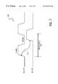
- FIG. 1shows a generalized example of a digital processing system using two cache memories.
- system 100comprises a processor ( 110 ) coupled to a main memory (DRAM 125 ) via I/O bus 120 .
- System 100also includes two cache memories (cache 105 and cache 115 ) coupled to processor 110 .
- Cache 115which is sometimes referred to as a level 2 cache, may be used to store a small subset of the data resident in DRAM 125 .
- cache 105which is sometimes referred to as a level 1 cache, may also be used to store a small subset of the data resident in DRAM 125 .
- cache 105is located on the same semiconductor substrate which includes processor 110 .
- cache 105 and cache 115allow processor 110 to bypass data transfers along I/O BUS 120 by providing a temporary storage medium.
- processor 110can update cache 105 and cache 115 without updating DRAM 125 —typically, when data is written only into a cache the cache is referred to as a write back cache.
- the use of write back cachesrequires that processor 110 includes additional logic and memory cells in the caches.
- the memory cells added to the cachesidentify whether a specific group of cache memory cells (referred to as a cache line) have been updated—the data stored in the additional memory cells is typically referred to as a “dirty bit.”
- FIG. 2shows a typical example of a write back cache memory.
- cache 200includes a tag array ( 230 ) and a data array ( 215 ) coupled to a decoder ( 210 ).
- Data array 215includes a group of cache lines ( 216 - 216 N) that store a copy of the data stored in main memory (for example DRAM 125 of FIG. 1 ).
- tag arrayincludes a group of tag lines ( 231 - 231 N) that determine the main memory location associated with data stored in data array 215 .
- cache 200includes decoder 210 .
- Decoder 210includes an address ( 205 ) input and a clock (CLK 206 ) input.
- a processor(for example processor 110 of FIG. 1) coupled to cache 200 uses decoder 210 to store or retrieve data from cache 200 .
- the processorgenerates a decoded address corresponding to a specific main memory address on address 205 .
- decoder 210determines whether the main memory address resides within cache 200 .
- decoder 210accesses a cache line in data array 215 and a tag line of tag array 230 via a word line.
- FIG. 2shows a word line (WL 225 ) used to access cache line 216 in data array 215 and tag line 231 in tag array 230 .
- FIG. 2also shows a dual port memory cell 240 included in tag line 231 .
- Dual port memory cell 240is coupled to decoder 210 via WL 225 and WL 226 .
- dual port memory cell 240stores a dirty bit indicating whether the information resident in the selected cache line is the updated version of the information resident in the main memory. Accordingly, the dirty bit allows a processor to determine which memory (main memory, a level one cache, or a level two cache) includes the most current data, thus reducing the chances of data corruption.
- dual port memory cellshave three functional modes—a read/modify write mode, a read only mode, and a write only mode. During the read/modify write mode, the dirty bit of the dual port memory cell is read and re-written in one clock cycle.
- word lines coupled to the dual port memoryhave a clock phase relation that increases the logic size of the decoder coupled to the dual port memory cell.
- a memory array structurecomprises a first word line coupled to a single port memory cell and a dual port memory cell.
- the memory array structurealso comprises a second word line coupled to the dual port memory cell.
- the second word lineis operable to control the data storage of the dual port memory during the second phase of a clock signal.
- the memory array structurealso comprises a decoder coupled to the dual port memory.
- the decoderhas a plurality of data input lines and a plurality of data output lines.
- the memory array structurefurther comprises a control logic coupled to the decoder. The control logic is operable to transfer data to the dual port memory from the plurality of data output lines during the second phase of a clock signal controlling a write operation.
- the memory array structurefurther comprises a word line driver coupled to the first word line and the second word line.
- the word line driveris operable to control the signal transitions of the second word line during a write operation.
- FIG. 1shows a generalized example of a digital processing system using two cache memories
- FIG. 2shows a typical example of a write back cache memory
- FIG. 3illustrates one embodiment of a dual port memory cell decoder and word line driver
- FIG. 4illustrates one embodiment of a word line driver
- FIG. 5illustrates one embodiment of a control logic used to determine, a write, read, or read/modify write operation
- FIG. 6illustrates one embodiment of a column decoder
- FIG. 7shows a timing diagram illustrating a write operation.
- a cache using a plurality of dual port memory cells with dedicated read and write linesis disclosed.
- a processor coupled to the cacheuses a two phase clock signal to synchronize data storage and data retrieval from the cache.
- the processoralso performs operations on the data stored in the plurality of dual port memory cells to indicate or determine whether cache lines associated with the plurality of dual port memory cells include valid or invalid data.
- the cacheincludes an array of cache lines, an array of dual port memory cells, an array of decoders, and an array of word lines. For illustrative purposes, however, the following description provides the logic and control signals associated with a single dual port memory cell.
- the processorperforms a read, a write, or a read/modify write operation on a dual port memory cell.
- a word line driveris configured to control the writing of data to the dual port memory cell during the second phase of a clock signal.
- control logic coupled to a decoder of the dual port memoryensures that data is written into the dual port memory during the second phase of the clock.
- FIG. 3illustrates one embodiment of a dual port memory cell decoder and a word line driver.
- system 300comprises a dual port memory cell (DP 325 ) coupled to a word line driver (WLD 310 ) and a column decoder ( 330 ).
- WLD 310is coupled to inputs 360 and CLK 350 .
- system 300is coupled to a processor (not shown) via inputs 360 and CLK 350 .
- the processorgenerates a decoded address on input 360 to perform a read, write, or read/modify write operation on the data stored in DP 325 .
- the processoruses CLK 350 to synchronize read, write, and read/modify write operations on DP 325 .
- System 300also comprises control logic 335 coupled to column decoder 330 .
- Column decoder 330is coupled to input data 336 and output data 335 .
- data 336 and data 335comprises multiple bit lines that are coupled to sense amplifiers (not shown) and write drivers (not shown), respectively.
- the sense amplifiersare used to read the data stored in DP 325 .
- the write driversare used to write data into DP 325 .
- DP 325is coupled to WLD 310 via word lines WL 315 and WL 320 .
- WL 315 and WL 320are used to read data from DP 325 and write data into DP 325 .
- WL 315controls the transfer of data from DP 325 onto lines R 328 and R# 329 .
- WL 320controls the transfer of data from lines W 326 and W# 327 into DP 325 .
- WL 320transitions in the second phase of CLK 350 .
- datais written into DP 325 during the second phase of CLK 350 .
- system 300is coupled to a data array single port memory cell (not shown) via WL 315 .
- WL 320is a dual port word line that controls the writing of data into DP 325 .
- WL 315is responsible for the writing of data into the single port memory cell, the reading of data from the single port memory cell, and the reading of data from DP 325 .
- the generation of a dual port word line (WL 320 ) that transitions during a second phase of a write operationallows a reduced decoder (column decoder 330 ) size because in a write operation WL 315 is used solely to control the operation of the single port memory cell.
- DP 325comprises a pair of cross-coupled inverters.
- the data on R# 329is the logical inverse of the data on R 328 and both R 328 and R# 329 form the first port of DP 325 .
- the data on W# 327is the logical inverse of the data on W 326 and both W 326 and W# 327 form the second port of DP 325 .
- DP 325is also coupled to column decoder 330 via lines R 328 , R# 329 , W 326 , and W# 327 .
- lines R 328 and R# 329are dedicated read lines. Accordingly, column decoder 330 selectively couples data 336 to lines R 328 and R# 329 based on a read enable (RE 345 ) control signal generated by control logic 335 .
- lines W 326 and W# 327are dedicated write lines. Accordingly, column decoder 330 selectively couples lines W 326 and W# 327 to data 335 based on a write enable (WE 340 ) control signal generated by control logic 335 .
- WE 340write enable
- FIG. 4illustrates one embodiment of a word line driver.
- word line driver 400generates two word lines WL 420 and WL 415 based on inputs CLK 450 and 460 .
- word line driver 400is coupled to a processor (not shown).
- the processoruses CLK 450 to synchronize communications between the processor and word line driver 400 .
- the processoralso generates a set of decoded address line on input 460 to select word line driver 400 . If the decoded address values select word line driver 400 , NAND gate 450 generate a logic ‘0’ value on node 470 . If the decoded address values does not select word line driver 400 , NAND gate 450 generates a logic ‘1’ value on node 470 .
- word line driver 400corresponds to WLD 310 of system 300 .
- WL 420corresponds to WL 320
- WL 415corresponds to WL 315
- CLK 450corresponds to CLK 350
- input 460corresponds to input 360 .
- input CLK 450is coupled to inverter 415 which, in turn, is coupled to inverter 425 , transistor 465 , and a first gate of pass gate 445 .
- Inverter 425is coupled to the second gate of passgate 445 .
- FIG. 4also illustrates that the two transmission points of passgate 445 are coupled to node 470 and inverter 435 .
- Inverter 435drives WL 420 .
- the coupling of CLK 450 to WL 420ensures that the logical inverse of the data on node 470 is transferred to WL 420 during the second phase of CLK 450 .
- Input CLK 450is also coupled to inverter 410 which, in turn, is coupled to inverter 420 , transistor 460 , and a second gate of pass gate 440 .
- the output of inverter 420is coupled to the first gate of passgate 440 .
- FIG. 4also illustrates that the two transmission points of passgate 440 are coupled to node 470 and inverter 430 .
- Inverter 430drives WL 415 .
- the coupling of CLK 450 to WL 415ensures that the logical inverse of the data on node 470 is transferred to WL 415 during the first phase of CLK 450 .
- FIG. 5illustrates one embodiment of a control logic used to determine a write, read, or read/modify write operation.
- control logic 500includes inputs READ 510 , WRITE 520 , CLK 550 , and DECODE 505 .
- Control logic 500also includes outputs WE 540 and RE 545 .
- CLK 550comprises signals PH 551 and PH 552 .
- CLK 550comprises a two phase clock signal.
- PH 551comprises a signal line carrying the first phase of the clock signal
- PH 552comprises a signal line carrying the second phase of the clock signal.
- control logic 500is coupled to a processor (not shown).
- the processoruses CLK 550 to synchronize communications between the processor and control logic 500 .
- the processoralso generates data on READ 510 and WRITE 520 to determine an operation. Specifically, during a write operation the processor generates a logic ‘1’ value on WRITE 520 and a logic ‘0’ value on READ 510 .
- the processorgenerates a logic ‘0’ value on WRITE 520 and a logic ‘1’ value on READ 510 .
- During a read/modify writethe processor generates a logic ‘1’ value on READ 510 .
- control logic 500may also disable control logic 500 via a logic ‘0’ value on input DECODER 505 .
- control logic 500corresponds to control logic 335 of system 300 . Accordingly, WE 540 corresponds to WE 340 , RE 545 corresponds to RE 345 , and CLK 550 corresponds to CLK 350 .
- output RE 545is generated by inverter 530 .
- the input of inverter 530is coupled to the output of NAND gate 525 which has three inputs coupled to READ 510 , PH 551 and DECODE 505 .
- Output WE 540is also generated by an inverter ( 575 ).
- the input of inverter 575is coupled to the output of NAND gate 570 whose inputs are generated by the output of NAND gate 560 and the output of NAND gate 564 .
- the inputs to NAND gate 560are READ 510 , DECODE 505 , and PH 552 .
- the inputs to NAND gate 565are WRITE 520 , DECODE 505 , and PH 552 .
- control logic 500is coupled to a column decoder of a dual port memory cell.
- the WE 540 signals generated by control logic 500ensure that column decoder transfers data to the dual port memory cell during the second phase of a write operation.
- the logic included in the column decoderis reduced because of the selective data transfer created by the control signals of control logic 500 .
- FIG. 6illustrates one embodiment of a column decoder.
- decoder 600includes a read path 605 A and a write path 605 B.
- decoder 600corresponds to column decoder 330 of system 300 .
- WE 640corresponds to WE 340
- RE 645corresponds to RE 345
- DATA 635corresponds to DATA 335
- DATA 636corresponds to DATA 336 .
- W 626corresponds to W 326
- W# 627corresponds to W# 327
- R 628corresponds to R 328
- R# 629corresponds to R# 329 .
- read path 605 Aincludes an inverter 610 with RE 645 as an input.
- the output of inverter 610is coupled to inverter 615 , the gate of transistor 625 , and the gate of transistor 630 .
- the source of transistor 625is coupled to input R 628 and the drain of transistor 625 is coupled to data 636 .
- the source of transistor 630is coupled to input R# 629 and the drain of transistor 630 is coupled to data 636 .
- the output of inverter 615is coupled to the gate of transistor 665 whose source and drain are coupled to R 628 and R# 629 , respectively.
- Write path 605 Bincludes an inverter 620 with WE 640 as an input.
- the output of inverter 620is coupled to the gate of transistor 650 , the gate of transistor 655 , and the gate of transistor 660 .
- the source of transistor 655is coupled to input W 626 and the drain of transistor 625 is coupled to data 635 .
- the source of transistor 650is coupled to input W# 627 and the drain of transistor 650 is coupled to data 635 .
- the source and drain of transistor 660are coupled to W 626 and W# 627 , respectively.
- column decoder 600is used in an array of multiple decoders. Accordingly, the dedicated read and write paths in conjunction with the control signals RE 645 and WE 640 allow for a simplified decoder design that reduces the sizes of the decoder array.
- WE 640ensures that during a write operation data transferred from data 635 to a dual port memory cell (not shown) occurs during the second phase of a processor clock.
- FIG. 7shows a timing diagram illustrating a write operation.
- timing diagram 700illustrates the relationship between clock signal CLK 710 and a dual port word line (WL 720 ).
- the transition of WL 720 with regards to the rising clock edge of CLK 710is illustrated by line 715 .
- WL 720transitions to a logic ‘1’ state only during the second phase of clock 710 .
- WL 720corresponds to WL 320 of system 300 .
- CLK 710(also shown as CLK 350 in system 300 ) corresponds to a processor clock signal used to synchronize data transfer between the processor, a cache including system 300 , and a single port memory of a data array.
- the transition of WL 720 during the second phase of a write operationallows a reduced decoder (column decoder 330 ) size because in a write operation the secondary word line driver (WL 315 ) is used solely to control the operation of the single port memory cell.
Landscapes
- Engineering & Computer Science (AREA)
- Theoretical Computer Science (AREA)
- Microelectronics & Electronic Packaging (AREA)
- Physics & Mathematics (AREA)
- General Engineering & Computer Science (AREA)
- General Physics & Mathematics (AREA)
- Static Random-Access Memory (AREA)
Abstract
Description
Claims (8)
Priority Applications (1)
| Application Number | Priority Date | Filing Date | Title |
|---|---|---|---|
| US09/277,659US6252818B1 (en) | 1999-03-26 | 1999-03-26 | Apparatus and method for operating a dual port memory cell |
Applications Claiming Priority (1)
| Application Number | Priority Date | Filing Date | Title |
|---|---|---|---|
| US09/277,659US6252818B1 (en) | 1999-03-26 | 1999-03-26 | Apparatus and method for operating a dual port memory cell |
Publications (1)
| Publication Number | Publication Date |
|---|---|
| US6252818B1true US6252818B1 (en) | 2001-06-26 |
Family
ID=23061842
Family Applications (1)
| Application Number | Title | Priority Date | Filing Date |
|---|---|---|---|
| US09/277,659Expired - LifetimeUS6252818B1 (en) | 1999-03-26 | 1999-03-26 | Apparatus and method for operating a dual port memory cell |
Country Status (1)
| Country | Link |
|---|---|
| US (1) | US6252818B1 (en) |
Cited By (5)
| Publication number | Priority date | Publication date | Assignee | Title |
|---|---|---|---|---|
| US20050083774A1 (en)* | 2003-10-16 | 2005-04-21 | International Business Machines Corporation | Method and apparatus for reducing power consumption in a memory array with dynamic word line driver/decoders |
| US20050254585A1 (en)* | 2004-05-13 | 2005-11-17 | International Business Machines Corporation | Self clock generation structure for low power local clock buffering decoder |
| US20090327620A1 (en)* | 2008-06-27 | 2009-12-31 | Igor Arsovski | Circuit structure and method for digital integrated circuit performance screening |
| US7831801B1 (en)* | 2006-08-30 | 2010-11-09 | Xilinx, Inc. | Direct memory access-based multi-processor array |
| US20170053706A1 (en)* | 2002-11-29 | 2017-02-23 | Kabushiki Kaisha Toshiba | Semiconductor memory device for storing multivalued data |
Citations (3)
| Publication number | Priority date | Publication date | Assignee | Title |
|---|---|---|---|---|
| US5835417A (en)* | 1994-11-22 | 1998-11-10 | Hitachi, Ltd. | Semiconductor device |
| US5973955A (en)* | 1998-02-02 | 1999-10-26 | Motorola, Inc. | Comparison circuit utilizing a differential amplifier |
| US5991230A (en)* | 1997-03-19 | 1999-11-23 | Kabushiki Kaisha Toshiba | Synchronous random access memory |
- 1999
- 1999-03-26USUS09/277,659patent/US6252818B1/ennot_activeExpired - Lifetime
Patent Citations (3)
| Publication number | Priority date | Publication date | Assignee | Title |
|---|---|---|---|---|
| US5835417A (en)* | 1994-11-22 | 1998-11-10 | Hitachi, Ltd. | Semiconductor device |
| US5991230A (en)* | 1997-03-19 | 1999-11-23 | Kabushiki Kaisha Toshiba | Synchronous random access memory |
| US5973955A (en)* | 1998-02-02 | 1999-10-26 | Motorola, Inc. | Comparison circuit utilizing a differential amplifier |
Cited By (14)
| Publication number | Priority date | Publication date | Assignee | Title |
|---|---|---|---|---|
| US10867686B2 (en) | 2002-11-29 | 2020-12-15 | Toshiba Memory Corporation | Semiconductor memory device for storing multivalued data |
| US11264108B2 (en) | 2002-11-29 | 2022-03-01 | Kioxia Corporation | Semiconductor memory device for storing multivalued data |
| US20170053706A1 (en)* | 2002-11-29 | 2017-02-23 | Kabushiki Kaisha Toshiba | Semiconductor memory device for storing multivalued data |
| US9881681B2 (en)* | 2002-11-29 | 2018-01-30 | Toshiba Memory Corporation | Semiconductor memory device for storing multivalued data |
| US10109358B2 (en) | 2002-11-29 | 2018-10-23 | Toshiba Memory Corporation | Semiconductor memory device for storing multivalued data |
| US10418117B2 (en) | 2002-11-29 | 2019-09-17 | Toshiba Memory Corporation | Semiconductor memory device for storing multivalued data |
| US10636502B2 (en) | 2002-11-29 | 2020-04-28 | Toshiba Memory Corporation | Semiconductor memory device for storing multivalued data |
| US6914849B2 (en)* | 2003-10-16 | 2005-07-05 | International Business Machines Corporation | Method and apparatus for reducing power consumption in a memory array with dynamic word line driver/decoders |
| US20050083774A1 (en)* | 2003-10-16 | 2005-04-21 | International Business Machines Corporation | Method and apparatus for reducing power consumption in a memory array with dynamic word line driver/decoders |
| US20050254585A1 (en)* | 2004-05-13 | 2005-11-17 | International Business Machines Corporation | Self clock generation structure for low power local clock buffering decoder |
| US7860172B2 (en)* | 2004-05-13 | 2010-12-28 | International Business Machines Corporation | Self clock generation structure for low power local clock buffering decoder |
| US7831801B1 (en)* | 2006-08-30 | 2010-11-09 | Xilinx, Inc. | Direct memory access-based multi-processor array |
| US20090327620A1 (en)* | 2008-06-27 | 2009-12-31 | Igor Arsovski | Circuit structure and method for digital integrated circuit performance screening |
| US8214699B2 (en) | 2008-06-27 | 2012-07-03 | International Business Machines Corporation | Circuit structure and method for digital integrated circuit performance screening |
Similar Documents
| Publication | Publication Date | Title |
|---|---|---|
| US6647478B2 (en) | Semiconductor memory device | |
| US5490114A (en) | High performance extended data out | |
| JP4524194B2 (en) | Simultaneous refresh mode with distributed row address counter in embedded DRAM | |
| US6556471B2 (en) | VDD modulated SRAM for highly scaled, high performance cache | |
| CN101286144A (en) | Multi-path accessible semiconductor memory device | |
| US6134178A (en) | Synchronous semiconductor memory device suitable for merging with logic | |
| JP5563056B2 (en) | Memory bus output driver for multi-bank memory device and method therefor | |
| WO2003007306A2 (en) | Method and system for banking register file memory arrays | |
| US6636443B2 (en) | Semiconductor memory device having row buffers | |
| JP2004111027A (en) | Multiport sram cell writing circuit and method | |
| US8032695B2 (en) | Multi-path accessible semiconductor memory device with prevention of pre-charge skip | |
| US6252818B1 (en) | Apparatus and method for operating a dual port memory cell | |
| JPH11126481A (en) | Semiconductor storage device | |
| US7349266B2 (en) | Memory device with a data hold latch | |
| US6002632A (en) | Circuits, systems, and methods with a memory interface for augmenting precharge control | |
| US5956286A (en) | Data processing system and method for implementing a multi-port memory cell | |
| US6839807B2 (en) | Multi-way set associative cache memory | |
| US20040264282A1 (en) | Predecode column architecture and method | |
| CN107025930B (en) | Address detector for enabling/disabling burst mode reads in SRAM | |
| EP0473819A1 (en) | Multiport memory cell | |
| KR20090005786A (en) | Multipath-accessible semiconductor memory device with memory usage expansion function and memory usage expansion method accordingly | |
| US7558924B2 (en) | Systems and methods for accessing memory cells | |
| JP2740486B2 (en) | Semiconductor storage device | |
| KR20010085667A (en) | Semiconductor memory device | |
| JPH09231758A (en) | Semiconductor memory device |
Legal Events
| Date | Code | Title | Description |
|---|---|---|---|
| AS | Assignment | Owner name:SAND CRAFT, INC., CALIFORNIA Free format text:ASSIGNMENT OF ASSIGNORS INTEREST;ASSIGNOR:VOSS, PETER;REEL/FRAME:010044/0691 Effective date:19990520 | |
| AS | Assignment | Owner name:VENTURE LENDING & LEASING II, INC., CALIFORNIA Free format text:ASSIGNMENT OF ASSIGNORS INTEREST;ASSIGNOR:SANDCRAFT, INC.;REEL/FRAME:010150/0674 Effective date:19990721 | |
| STCF | Information on status: patent grant | Free format text:PATENTED CASE | |
| AS | Assignment | Owner name:RAZA MICROELECTRONICS, INC., CALIFORNIA Free format text:ASSIGNMENT OF ASSIGNORS INTEREST;ASSIGNOR:SANDCRAFT, INC.;REEL/FRAME:014624/0967 Effective date:20030729 | |
| FEPP | Fee payment procedure | Free format text:PAT HOLDER CLAIMS SMALL ENTITY STATUS, ENTITY STATUS SET TO SMALL (ORIGINAL EVENT CODE: LTOS); ENTITY STATUS OF PATENT OWNER: LARGE ENTITY | |
| FPAY | Fee payment | Year of fee payment:4 | |
| AS | Assignment | Owner name:VENTURE LENDING & LEASING IV, INC., AS AGENT FOR I Free format text:SECURITY INTEREST;ASSIGNOR:RAZA MICROELECTRONICS, INC.;REEL/FRAME:016116/0147 Effective date:20041214 | |
| AS | Assignment | Owner name:VENTURE LENDING & LEASING IV, INC., CALIFORNIA Free format text:SECURITY INTEREST;ASSIGNOR:RAZA MICROELECTRONICS, INC.;REEL/FRAME:019224/0254 Effective date:20061226 | |
| FEPP | Fee payment procedure | Free format text:PAYOR NUMBER ASSIGNED (ORIGINAL EVENT CODE: ASPN); ENTITY STATUS OF PATENT OWNER: LARGE ENTITY | |
| FEPP | Fee payment procedure | Free format text:PAT HOLDER NO LONGER CLAIMS SMALL ENTITY STATUS, ENTITY STATUS SET TO UNDISCOUNTED (ORIGINAL EVENT CODE: STOL); ENTITY STATUS OF PATENT OWNER: LARGE ENTITY | |
| AS | Assignment | Owner name:RMI CORPORATION, CALIFORNIA Free format text:CHANGE OF NAME;ASSIGNOR:RAZA MICROELECTRONICS, INC.;REEL/FRAME:020951/0633 Effective date:20071217 | |
| FEPP | Fee payment procedure | Free format text:PAT HOLDER NO LONGER CLAIMS SMALL ENTITY STATUS, ENTITY STATUS SET TO UNDISCOUNTED (ORIGINAL EVENT CODE: STOL); ENTITY STATUS OF PATENT OWNER: LARGE ENTITY | |
| FPAY | Fee payment | Year of fee payment:8 | |
| FEPP | Fee payment procedure | Free format text:PAYER NUMBER DE-ASSIGNED (ORIGINAL EVENT CODE: RMPN); ENTITY STATUS OF PATENT OWNER: LARGE ENTITY Free format text:PAYOR NUMBER ASSIGNED (ORIGINAL EVENT CODE: ASPN); ENTITY STATUS OF PATENT OWNER: LARGE ENTITY | |
| AS | Assignment | Owner name:NETLOGIC MICROSYSTEMS, INC.,CALIFORNIA Free format text:ASSIGNMENT OF ASSIGNORS INTEREST;ASSIGNOR:RMI CORPORATION;REEL/FRAME:023926/0338 Effective date:20091229 Owner name:NETLOGIC MICROSYSTEMS, INC., CALIFORNIA Free format text:ASSIGNMENT OF ASSIGNORS INTEREST;ASSIGNOR:RMI CORPORATION;REEL/FRAME:023926/0338 Effective date:20091229 | |
| AS | Assignment | Owner name:NETLOGIC MICROSYSTEMS, INC., CALIFORNIA Free format text:RELEASE BY SECURED PARTY;ASSIGNOR:VENTURE LENDING & LEASING, INC;REEL/FRAME:026855/0108 Effective date:20110902 | |
| FPAY | Fee payment | Year of fee payment:12 | |
| AS | Assignment | Owner name:NETLOGIC I LLC, DELAWARE Free format text:CHANGE OF NAME;ASSIGNOR:NETLOGIC MICROSYSTEMS, INC.;REEL/FRAME:035443/0824 Effective date:20130123 Owner name:BROADCOM CORPORATION, CALIFORNIA Free format text:ASSIGNMENT OF ASSIGNORS INTEREST;ASSIGNOR:NETLOGIC I LLC;REEL/FRAME:035443/0763 Effective date:20150327 | |
| AS | Assignment | Owner name:BANK OF AMERICA, N.A., AS COLLATERAL AGENT, NORTH CAROLINA Free format text:PATENT SECURITY AGREEMENT;ASSIGNOR:BROADCOM CORPORATION;REEL/FRAME:037806/0001 Effective date:20160201 Owner name:BANK OF AMERICA, N.A., AS COLLATERAL AGENT, NORTH Free format text:PATENT SECURITY AGREEMENT;ASSIGNOR:BROADCOM CORPORATION;REEL/FRAME:037806/0001 Effective date:20160201 | |
| AS | Assignment | Owner name:AVAGO TECHNOLOGIES GENERAL IP (SINGAPORE) PTE. LTD., SINGAPORE Free format text:ASSIGNMENT OF ASSIGNORS INTEREST;ASSIGNOR:BROADCOM CORPORATION;REEL/FRAME:041706/0001 Effective date:20170120 Owner name:AVAGO TECHNOLOGIES GENERAL IP (SINGAPORE) PTE. LTD Free format text:ASSIGNMENT OF ASSIGNORS INTEREST;ASSIGNOR:BROADCOM CORPORATION;REEL/FRAME:041706/0001 Effective date:20170120 | |
| AS | Assignment | Owner name:BROADCOM CORPORATION, CALIFORNIA Free format text:TERMINATION AND RELEASE OF SECURITY INTEREST IN PATENTS;ASSIGNOR:BANK OF AMERICA, N.A., AS COLLATERAL AGENT;REEL/FRAME:041712/0001 Effective date:20170119 | |
| AS | Assignment | Owner name:AVAGO TECHNOLOGIES INTERNATIONAL SALES PTE. LIMITE Free format text:ASSIGNMENT OF ASSIGNORS INTEREST;ASSIGNOR:AVAGO TECHNOLOGIES GENERAL IP (SINGAPORE) PTE. LTD.;REEL/FRAME:047022/0620 Effective date:20180509 | |
| AS | Assignment | Owner name:AVAGO TECHNOLOGIES INTERNATIONAL SALES PTE. LIMITE Free format text:CORRECTIVE ASSIGNMENT TO CORRECT THE NATURE OF CONVEYANCE AND EFFECTIVE DATE PREVIOUSLY RECORDED ON REEL 047022 FRAME 0620. ASSIGNOR(S) HEREBY CONFIRMS THE MERGER;ASSIGNOR:AVAGO TECHNOLOGIES GENERAL IP (SINGAPORE) PTE. LTD.;REEL/FRAME:047185/0643 Effective date:20180509 | |
| AS | Assignment | Owner name:AVAGO TECHNOLOGIES INTERNATIONAL SALES PTE. LIMITE Free format text:CORRECTIVE ASSIGNMENT TO CORRECT THE EFFECTIVE DATE PREVIOUSLY RECORDED ON REEL 047185 FRAME 0643. ASSIGNOR(S) HEREBY CONFIRMS THE MERGER;ASSIGNOR:AVAGO TECHNOLOGIES GENERAL IP (SINGAPORE) PTE. LTD.;REEL/FRAME:047476/0845 Effective date:20180905 | |
| AS | Assignment | Owner name:AVAGO TECHNOLOGIES INTERNATIONAL SALES PTE. LIMITE Free format text:CORRECTIVE ASSIGNMENT TO CORRECT THE EFFECTIVE DATE OF MERGER PREVIOUSLY RECORDED AT REEL: 047185 FRAME: 0643. ASSIGNOR(S) HEREBY CONFIRMS THE CORRECTIVE MERGER;ASSIGNOR:AVAGO TECHNOLOGIES GENERAL IP (SINGAPORE) PTE. LTD.;REEL/FRAME:047959/0296 Effective date:20180905 |