US6252800B1 - Semiconductor memory device - Google Patents
Semiconductor memory deviceDownload PDFInfo
- Publication number
- US6252800B1 US6252800B1US09/448,172US44817299AUS6252800B1US 6252800 B1US6252800 B1US 6252800B1US 44817299 AUS44817299 AUS 44817299AUS 6252800 B1US6252800 B1US 6252800B1
- Authority
- US
- United States
- Prior art keywords
- valid
- invalid information
- block
- storage unit
- data
- Prior art date
- Legal status (The legal status is an assumption and is not a legal conclusion. Google has not performed a legal analysis and makes no representation as to the accuracy of the status listed.)
- Expired - Lifetime
Links
Images


Classifications
- G—PHYSICS
- G11—INFORMATION STORAGE
- G11C—STATIC STORES
- G11C16/00—Erasable programmable read-only memories
- G—PHYSICS
- G11—INFORMATION STORAGE
- G11C—STATIC STORES
- G11C29/00—Checking stores for correct operation ; Subsequent repair; Testing stores during standby or offline operation
- G11C29/04—Detection or location of defective memory elements, e.g. cell constructio details, timing of test signals
- G11C29/08—Functional testing, e.g. testing during refresh, power-on self testing [POST] or distributed testing
- G11C29/12—Built-in arrangements for testing, e.g. built-in self testing [BIST] or interconnection details
- G11C29/44—Indication or identification of errors, e.g. for repair
- G—PHYSICS
- G11—INFORMATION STORAGE
- G11C—STATIC STORES
- G11C29/00—Checking stores for correct operation ; Subsequent repair; Testing stores during standby or offline operation
- G11C29/04—Detection or location of defective memory elements, e.g. cell constructio details, timing of test signals
- G11C29/08—Functional testing, e.g. testing during refresh, power-on self testing [POST] or distributed testing
- G11C29/12—Built-in arrangements for testing, e.g. built-in self testing [BIST] or interconnection details
- G11C2029/1208—Error catch memory
Definitions
- the present inventiongenerally relates to semiconductor memory devices, and, more particularly, to a non-volatile semiconductor device which is electrically erasable and rewritable.
- flash memoryvarious types of flash EEPROM (hereinafter referred to as “flash memory”) have been developed as non-volatile semiconductor memory devices which are electrically erasable and rewritable.
- flash memorycell-type flash memory (hereinafter referred to as “NAND-type flash memory”) has been used for files to store a large amount of data, and its memory capacity has been increasing.
- NAND-type flash memoryAs the memory capacity of the NAND-type flash memory has increased, the number of memory cell transistors for storing information in the NAND-type flash memory has also increased. For instance, a flash memory having a 16-Mbit capacity contains 16,777,216 memory cell transistors, and a flash memory having a 64-Mbit capacity contains 67,108,864 memory cell transistors.
- a product quality testis performed on every memory cell transistor after the completion of the NAND-type flash memory.
- the NAND-type flash memoryperforms erasure by the block, which is a group of memory cell transistors.
- a block consisting of memory cell transistors judged to be defective through the product quality testis called a bad block (invalid block).
- Invalid blockA block consisting of memory cell transistors judged to be defective through the product quality test.
- Such a bad blockmight occur during the operation of the flash memory. Once a bad block is spotted, no access is allowed to the bad block.
- Information indicating whether the blocks are valid or invalidis called block valid/invalid information.
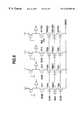
- FIG. 1is a block diagram of a conventional NAND-type flash memory.
- This block diagramincludes a row address buffer 10 , a column address buffer 12 , an address register 14 , a select Tr decoder 16 , a row address decoder 18 , a column address decoder 20 , a control and high-voltage circuit 22 , a command register 24 , a memory cell array 26 , a Y gate 28 , a sense amplifier 30 , a data register 32 , and an input/output control circuit 34 .
- the entire operation of the NAND-type flash memoryis controlled by a command signal.
- the command signal, an address signal, and a data signalare supplied to the input/output control circuit 34 via input/output terminals i/o 0 to i/o 7 .
- the input/output control circuit 34sends the supplied command signal, address signal, and data signal to the command register 24 , the address register 14 , and the data register 32 , respectively, in accordance with the combination of control signals supplied to the control and high-voltage circuit 22 .
- the command register 24latches the supplied command signal, and supplies the latched command signal to the control and high-voltage circuit 22 at desired timing.
- the control and high-voltage circuit 22then decodes the command signal, and outputs a control signal to the row address decoder 18 , the memory cell array 26 , the sense amplifier 30 , or the data register 32 , whichever is required to perform a process based on the command signal.
- the address register 14latches the supplied address signal, and supplies the latched address signal to the row address buffer 10 and the column address buffer 12 at desired timing.
- the row address buffer 10 supplied with the address signal from the address register 14sends the address signal to the select Tr decoder 16 and the row address decoder 18 at desired timing.
- the column address buffer 12 supplied with the address signal from the address register 14sends the address signal to the column address decoder 20 at desired timing.
- the select Tr decoder 16outputs a select transistor control signal SL for controlling select transistors included in the memory cell array 26 based on the address signal.
- the row address decoder 18decodes the supplied address signal to output a word line signal WL.
- a data signal selected from cell blocks constituting the memory cell array 26is sent to the Y gate 28 .
- the column address decoder 20decodes the supplied address signal to output a signal for controlling the Y gate 28 .
- the Y gate 28selects a necessary data signal from data signals supplied from the memory cell array 26 , and supplies the selected data signal to the data register 32 via the sense amplifier 30 .
- the data register 32latches the data signal supplied through the sense amplifier 30 , and then sends the data signal to the input/output control circuit 34 at desired timing.
- the input/output control circuit 34sequentially outputs data signals in accordance with a clock signal.
- FIG. 2is a timing chart of a data signal reading operation of the NAND-type flash memory of FIG. 1 .
- signals provided with “/”are negative logic signals, and the other signals are positive logic signals.
- a command signal, address signals, and data signalsare supplied to the input/output control circuit 34 based on the timing of a write enable signal /WE.
- the type of the signal to be supplied to the input/output control circuit 34is determined in accordance with a command latch enable signal CLE and an address latch enable signal ALE supplied to the control and high-voltage circuit 22 . More specifically, a signal supplied to the input/output control circuit 34 at the same time as the command latch enable signal CLE is a command signal, and a signal supplied to the input/output control circuit 34 at the same time as the address latch enable signal ALE is an address signal. Accordingly, a command signal ( 00 H) and address signals (A 0 to A 22 ) are supplied to the input/output control circuit 34 in the timing chart of FIG. 2 .
- Data signalsare then read from the memory cell array 26 , and are outputted sequentially from the input/output control circuit 34 via the Y gate 28 , the sense amplifier 30 , and the data register 32 , in accordance with the timing of a read enable signal /RE.
- the management sidepossesses the block valid/invalid information of the blocks. Therefore, it is necessary to produce a table of the block valid/invalid information for each block.
- the block valid/invalid information of each blockis coded and written in a predetermined position in each corresponding block. Each block is judged whether it is a bad block from the code written in the predetermined position.
- the management sideWhen producing a table of the block valid/invalid information, the management side reads out the data of the memory cells of all the blocks, and produces the table of the block valid/invalid information based on the block valid/invalid information contained in the read data. In accordance with the table of the block valid/invalid information, the management side disables access to bad blocks. The table of the block valid/invalid information is updated when a new bad block occurs during an operation of the NAND-type flash memory 1 .
- the NAND-type flash memoryis read by the page, for instance, which is a unit of data of one word line, and reading one page of data from the memory cells into the data register 32 requires a certain period of time. Accordingly, producing a table of block valid/invalid information for a larger number of blocks takes a longer period of time.
- a general object of the present inventionis to provide a semiconductor memory device in which the above disadvantages are eliminated.
- a more specific object of the present inventionis to provide a semiconductor memory device which enables high-speed and accurate reading of block valid/invalid information.
- a semiconductor memory devicecomprising: a memory cell array including blocks, each of the blocks having memory cells arranged in rows and columns; and a valid/invalid information storage unit which is connected to the memory cell array and stores pieces of valid/invalid information respectively indicating whether the blocks are valid or invalid.
- the valid/invalid information storage unit that stores the valid/invalid informationis independent of the memory cells, and accurate reading of the valid/invalid information can be performed at high speed.
- the amount of data of the valid/invalid information stored in the valid/invalid information storage unitis far smaller than the amount of data stored in the memory cells, and the constitution of the valid/invalid information storage unit is simpler accordingly.
- the valid/invalid information storage unitenables high-speed and accurate reading of the valid/invalid information.
- FIG. 1is a block diagram of a NAND-type flash memory of the prior art
- FIG. 2is a timing chart of a data signal reading operation of the NAND-type flash memory
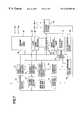
- FIG. 3is a block diagram of a first embodiment of a semiconductor memory device of the present invention.
- FIG. 4is a circuit diagram of a bad-block storage of the first embodiment of the present invention.
- FIG. 5is a block diagram of a second embodiment of a semiconductor memory device of the present invention.
- FIG. 6is a circuit diagram of a bad-block storage of the second embodiment of the present invention.
- FIG. 7is a block diagram of a third embodiment of a semiconductor memory device of the present invention.
- FIG. 3is a block diagram of a first embodiment of a semiconductor memory device of the present invention.
- the same components as in the block diagram of FIG. 1are indicated by the same reference numerals.
- a semiconductor memory device 2 of the present invention shown in FIG. 3includes a bad-block storage unit 40 which is not shown in the diagram of FIG. 1 .
- the bad-block storage unit 40comprises a bad-block storage 41 , a Y gate 42 , and a sense amplifier 43 .
- the Y gates 28 and 42conduct switching between the bad-block storage 41 and the memory cell array 26 . In accordance with a command signal or a high-voltage signal supplied to the control and high-voltage circuit 22 , the switching is performed between the Y gates 28 and 42 .
- a signal for selecting from data stored in the bad-block storage 41is supplied from the row address decoder 18 in the same way that a signal is supplied to the memory cell array 26 .
- the block valid/invalid information corresponding to a subject blockis read out.
- the block valid/invalid information that has been conventionally written in a predetermined position in each blockcan be written in the bad-block storage unit 40 .
- the block valid/invalid informationrequires only 1 bit for each block. If the block valid/invalid information for a subject block is “0”, the block is a bad block. If the block valid/invalid information is “1”, the block is not a bad block. However, in a case where a decision-by-majority system using a plurality of bits is employed to improve the reliability, one block should consist of the same number of bits. In the decision-by-majority system using a plurality of bits, if 3-bit block valid/invalid information is “0, 0, 1”, for instance, the corresponding block is judged to be “0”, i.e., a bad block.
- the bad-block storage unit 40stores a far smaller amount of data than the memory cell array 26 , and can be made simpler in design while achieving high reliability.
- the bad-block storage unit 40 of the present inventiondramatically reduces the amount of data to be read out, and thus speeds up the process.
- FIG. 4shows the bad-block storage 41 of the bad-block storage unit 40 of the first embodiment.
- the bad-block storage unit 40 in this embodimentstores the block valid/invalid information of 1024 blocks.
- the bad-block storage 41 of FIG. 4includes: memory cells BBC 0 to BBC 1023 which store the block valid/invalid information; word lines WLB 0 , WLB 16 , WLB 32 , . . .
- WLB 16367for the bad-block storage corresponding to the addresses of the respective blocks; select transistors TrD 0 to TrD 1023 for controlling the connection between the memory cells BBC 0 to BBC 1023 and a bit line; signal conductors SLDB 0 to SLDB 1023 for the select transistors TrD 0 to TrD 1023 ; select transistors TrS 0 to TrS 1023 for controlling the connection between the memory cells BBC 0 to BBC 1023 and the array (GND); and signal conductors SLSB 0 to SLSB 1023 for the select transistors TrS 0 to TrS 1023 .
- the select transistors TrDn, the memory cells BBCn, and the select transistors TrSnare connected in series, and the memory cells BBCn correspond to the block valid/invalid information on a one-for-one basis.
- “n”indicates one of the numbers from 0 to 1023.
- the select transistors TrDn, the memory cells BBCn, and the select transistors TrSncorrespond to the select transistors TrDn, the memory cells BBCn, and the select transistors TrSn of the memory cell array 26 , respectively.
- the Y gate 42 and the sense amplifier 43also correspond to the Y gate 28 and the sense amplifier 30 , respectively. Writing, erasing, and reading can be carried out in the bad-block storage 41 as well as in the memory cell array 26 .
- the operation modeis switched to a bad block mode.
- the bad block modethe block valid/invalid information is read out from the bad-block storage unit 40 .
- the row address decoder 18decodes a supplied address signal to generate a block address signal, and the word line WLBn for the bad-block storage corresponding to the block address signal is selected.
- the select transistor TrDn and the select transistor TrSn corresponding to the block address signalare controlled when necessary.
- the memory cell BBCn corresponding to the block address signalis selected, and the condition of the selected memory cell BBCn is read out. Fluctuations in the level of the bit line are sent to the sense amplifier 43 via the Y gate 42 , and the sense amplifier 43 judges the block valid/invalid information stored in the memory cell BBCn. For instance, if the current does not flow through the memory cell BBCn, the condition is judged to be “0”, i.e., a bad block, and if the current flows through the memory cell BBCn, the condition is judged to be “1”, i.e., not a bad block.
- the block valid/invalid informationindicates a bad block.
- the sense amplifier 43detects level fluctuations, the block valid/invalid information does not indicate a bad block.
- the block valid/invalid information judged by the sense amplifier 43is then latched by the data register 32 , and is outputted along with a clock signal to the outside via the input/output control circuit 34 .
- FIG. 5is a block diagram of the second embodiment of a semiconductor memory device of the present invention.
- the same components as in the block diagram of FIG. 3are indicated by the same reference numerals.
- a semiconductor memory device 3 shown in FIG. 5differs from the semiconductor memory device 2 shown in FIG. 3 in the structure of the bad-block storage unit.
- a bad-block storage unit 50 of this embodimentcomprises a bad-block storage 51 , a Y gate 52 , and a sense amplifier 53 .
- the Y gates 28 and 52conduct switching between the bad-block storage 51 and the memory cell array 26 .
- the switchingis performed between the Y gates 28 and 52 .
- a signal for selecting from data in the bad-block storage 51is supplied from the row address decoder 18 , and the block valid/invalid information corresponding to a subject block is read out. With this structure, the block valid/invalid information that has been written in a predetermined position in each block can be written in the bad-block storage unit 50 .
- FIG. 6is a circuit diagram of the bad-block storage unit of the second embodiment.
- the bad-block storage unit 50also stores the block valid/invalid information of 1024 blocks.
- the bad-block storage 51 of FIG. 6is a circuit diagram of the bad-block storage unit of the second embodiment.
- the bad-block storage unit 50also stores the block valid/invalid information of 1024 blocks.
- the bad-block storage 51 of FIG. 6is a circuit diagram of the bad-block storage unit of the second embodiment.
- the bad-block storage unit 50also stores the block valid/invalid information of 1024 blocks.
- memory cells BBC 0 to BBC 1023which store the block valid/invalid information
- bit lines BLB 0 to BLB 1023for the bad-block storage corresponding to the addresses of the respective blocks
- select transistors 52 - 1 to 52 - 1023for controlling the connection among the bit lines BLB 0 to BLB 1023 for the bad-block storage
- a word line WLBfor the back block storage
- select transistors TrD 0 to TrD 1023for controlling the connection between the memory cells BBC 0 to BBC 1023 and the bit lines BLB 0 to BLB 1023
- a signal conductor SLDBfor the select transistors TrD 0 to TrD 1023
- select transistors TrS 0 to TrS 1023for controlling the connection between the memory cells BBC 0 to BBC 1023 and the array (GND); and a signal conductor SLSB for the select transistors TrS 0 to TrS 1023 .
- the select transistors TrDn, the memory cells BBCn, and the select transistors TrSnare connected in series, and the memory cells BBCn correspond to the block valid/invalid information on a one-for-one basis.
- “n”indicates one of the numbers from 0 to 1023.
- the select transistors TrDn, the memory cells BBCn, and the select transistors TrSncorrespond to the select transistors TrDn, the memory cells BBCn, and the select transistors TrSn of the memory cell array 26 , respectively.
- the Y gate 52 and the sense amplifier 53also correspond to the Y gate 28 and the sense amplifier 30 , respectively. Writing, erasing, and reading can be carried out in the bad-block storage 51 as well as in the memory cell array 26 .
- the operation modeis switched to a bad block mode.
- the bad block modethe block valid/invalid information is read out from the bad-block storage unit 50 .
- the row address decoder 18decodes a supplied address signal to generate a block address signal, and the bit line BLBn for the bad-block storage corresponding to the block address signal is selected.
- the block valid/invalid information of a corresponding blockis read out.
- a plurality of bit lines BLBn or all of the bit lines BLBncan be selected, for instance, by latching, so that the block valid/invalid information of a plurality of blocks or all of the blocks can be read out simultaneously.
- the block valid/invalid information corresponding to the block addresscan be read from the memory cell BBCn to the selected bit line. Fluctuations in the level of the bit lines are sent to the sense amplifier 53 via the select transistor 52 -n, and the sense amplifier 53 judges the block valid/invalid information stored in the memory cell BBCn. The block valid/invalid information judged by the sense amplifier 53 is then latched by the data register 32 , and is outputted along with a clock signal to the outside via the input/output control circuit 34 .
- the block valid/invalid information of a plurality of blocks or all of the blockscan be supplied to the data register 32 at once. Compared with the circuit diagram of FIG. 4, the bit lines of FIG. 6 are shorter, and so is the charging time. After the block valid/invalid information of a plurality of blocks or all of the blocks is supplied to the data register 32 , the block valid/invalid information is read out sequentially with the clock signal. Thus, the block valid/invalid information can be read at higher speed.
- FIG. 7is a block diagram of the third embodiment of the semiconductor memory device of the present invention.
- the same components as in the block diagram of FIG. 5are indicated by the same reference numerals.
- the block diagram of a semiconductor memory device 4 of FIG. 7includes an ECC (Error Correction Code) generation circuit 60 , an ECC storage unit 61 , and an ECC comparison circuit 62 .
- ECCError Correction Code
- the datais sent to the data register 32 via the input/output control circuit 34 , and the same data is sent to the ECC generation circuit 60 to produce an ECC ( 1 ).
- the data register 32writes the data in a predetermined block in the memory cell array 26 .
- the ECC generation circuit 60stores the ECC ( 1 ) in the ECC storage unit 61 .
- the ECC ( 1 ) stored in the ECC storage unit 61is associated with the block in which the original data of the ECC ( 1 ) is stored.
- the structure of the ECC storage unit 61can be the same as the bad-block storage unit 50 .
- the dataWhen data is read out, the data is read from the memory cell array 26 , and is supplied to the data register 32 .
- the data register 32holds the data sent from the memory cell array 26 , and also supplies the same data to the ECC generation circuit 60 to generate an ECC ( 2 ).
- the ECC generation circuit 60then supplies the generated ECC ( 2 ) to the ECC comparison circuit 62 .
- the ECC storage unit 61supplies the ECC comparison circuit 62 with the ECC ( 1 ) of the data to be read out.
- the ECC comparison circuit 62compares the ECC ( 1 ) with the ECC ( 2 ). If the ECC ( 1 ) coincides with the ECC ( 2 ), the data held in the data register 32 is outputted to the outside via the input/output control circuit 34 .
Landscapes
- Read Only Memory (AREA)
- For Increasing The Reliability Of Semiconductor Memories (AREA)
- Techniques For Improving Reliability Of Storages (AREA)
Abstract
Description
Claims (9)
Applications Claiming Priority (2)
| Application Number | Priority Date | Filing Date | Title |
|---|---|---|---|
| JP10-332884 | 1998-11-24 | ||
| JP33288498AJP3730423B2 (en) | 1998-11-24 | 1998-11-24 | Semiconductor memory device |
Publications (1)
| Publication Number | Publication Date |
|---|---|
| US6252800B1true US6252800B1 (en) | 2001-06-26 |
Family
ID=18259884
Family Applications (1)
| Application Number | Title | Priority Date | Filing Date |
|---|---|---|---|
| US09/448,172Expired - LifetimeUS6252800B1 (en) | 1998-11-24 | 1999-11-24 | Semiconductor memory device |
Country Status (4)
| Country | Link |
|---|---|
| US (1) | US6252800B1 (en) |
| JP (1) | JP3730423B2 (en) |
| KR (1) | KR100616345B1 (en) |
| TW (1) | TW538413B (en) |
Cited By (29)
| Publication number | Priority date | Publication date | Assignee | Title |
|---|---|---|---|---|
| US6510090B1 (en)* | 2001-10-03 | 2003-01-21 | Fujitsu Limited | Semiconductor memory device |
| US20040190347A1 (en)* | 2001-09-17 | 2004-09-30 | Raul-Adrian Cernea | Dynamic column block selection |
| US20040190338A1 (en)* | 2003-03-28 | 2004-09-30 | Hynix Semiconductor Inc. | Structure for testing NAND flash memory and method of testing NAND flash memory |
| US6901498B2 (en) | 2002-12-09 | 2005-05-31 | Sandisk Corporation | Zone boundary adjustment for defects in non-volatile memories |
| US20050141387A1 (en)* | 2003-12-31 | 2005-06-30 | Raul-Adrian Cernea | Flexible and area efficient column redundancy for non-volatile memories |
| US20050188148A1 (en)* | 2004-02-20 | 2005-08-25 | Nec Electronics Corporation | Data access controlling method in flash memory and data access controlling program |
| US20070103977A1 (en)* | 2005-11-08 | 2007-05-10 | Conley Kevin M | Retargetable memory cell redundancy methods |
| US20100309720A1 (en)* | 2009-06-05 | 2010-12-09 | Bo Liu | Structure and Method for Shuffling Data Within Non-Volatile Memory Devices |
| US20100309719A1 (en)* | 2009-06-05 | 2010-12-09 | Yan Li | Folding Data Stored in Binary Format Into Multi-State Format Within Non-Volatile Memory Devices |
| US20100329007A1 (en)* | 2009-06-24 | 2010-12-30 | Hardwell Chibvongodze | Pointer Based Column Selection Techniques in Non-Volatile Memories |
| US20110002169A1 (en)* | 2009-07-06 | 2011-01-06 | Yan Li | Bad Column Management with Bit Information in Non-Volatile Memory Systems |
| US20110153913A1 (en)* | 2009-12-18 | 2011-06-23 | Jianmin Huang | Non-Volatile Memory with Multi-Gear Control Using On-Chip Folding of Data |
| US8144512B2 (en) | 2009-12-18 | 2012-03-27 | Sandisk Technologies Inc. | Data transfer flows for on-chip folding |
| TWI395228B (en)* | 2004-12-24 | 2013-05-01 | Spansion Llc | Method and apparatus for applying bias to a storage device |
| US8681548B2 (en) | 2012-05-03 | 2014-03-25 | Sandisk Technologies Inc. | Column redundancy circuitry for non-volatile memory |
| US8725935B2 (en) | 2009-12-18 | 2014-05-13 | Sandisk Technologies Inc. | Balanced performance for on-chip folding of non-volatile memories |
| US8842473B2 (en) | 2012-03-15 | 2014-09-23 | Sandisk Technologies Inc. | Techniques for accessing column selecting shift register with skipped entries in non-volatile memories |
| US8897080B2 (en) | 2012-09-28 | 2014-11-25 | Sandisk Technologies Inc. | Variable rate serial to parallel shift register |
| US8971115B2 (en) | 2013-03-01 | 2015-03-03 | Kabushiki Kaisha Toshiba | Semiconductor memory device |
| US9076506B2 (en) | 2012-09-28 | 2015-07-07 | Sandisk Technologies Inc. | Variable rate parallel to serial shift register |
| US9224502B1 (en) | 2015-01-14 | 2015-12-29 | Sandisk Technologies Inc. | Techniques for detection and treating memory hole to local interconnect marginality defects |
| US9269446B1 (en) | 2015-04-08 | 2016-02-23 | Sandisk Technologies Inc. | Methods to improve programming of slow cells |
| US9342446B2 (en) | 2011-03-29 | 2016-05-17 | SanDisk Technologies, Inc. | Non-volatile memory system allowing reverse eviction of data updates to non-volatile binary cache |
| US9490035B2 (en) | 2012-09-28 | 2016-11-08 | SanDisk Technologies, Inc. | Centralized variable rate serializer and deserializer for bad column management |
| US9564219B2 (en) | 2015-04-08 | 2017-02-07 | Sandisk Technologies Llc | Current based detection and recording of memory hole-interconnect spacing defects |
| US9934872B2 (en) | 2014-10-30 | 2018-04-03 | Sandisk Technologies Llc | Erase stress and delta erase loop count methods for various fail modes in non-volatile memory |
| US10032524B2 (en) | 2015-02-09 | 2018-07-24 | Sandisk Technologies Llc | Techniques for determining local interconnect defects |
| US10394479B2 (en)* | 2015-08-20 | 2019-08-27 | Micron Technology, Inc. | Solid state storage device with quick boot from NAND media |
| JP2021508140A (en)* | 2017-12-29 | 2021-02-25 | マイクロン テクノロジー,インク. | Uncorrectable ECC |
Families Citing this family (5)
| Publication number | Priority date | Publication date | Assignee | Title |
|---|---|---|---|---|
| JP3916862B2 (en) | 2000-10-03 | 2007-05-23 | 株式会社東芝 | Nonvolatile semiconductor memory device |
| JP4062247B2 (en) | 2003-12-11 | 2008-03-19 | ソニー株式会社 | Semiconductor memory device |
| JP4690747B2 (en) | 2005-03-09 | 2011-06-01 | 株式会社東芝 | Semiconductor memory device and driving method of semiconductor memory device |
| JP5032155B2 (en) | 2007-03-02 | 2012-09-26 | 株式会社東芝 | Nonvolatile semiconductor memory device and nonvolatile semiconductor memory system |
| US20150169438A1 (en)* | 2013-12-18 | 2015-06-18 | Infineon Technologies Ag | Method and device for incrementing an erase counter |
Citations (4)
| Publication number | Priority date | Publication date | Assignee | Title |
|---|---|---|---|---|
| US5563828A (en)* | 1994-12-27 | 1996-10-08 | Intel Corporation | Method and apparatus for searching for data in multi-bit flash EEPROM memory arrays |
| US5930815A (en)* | 1995-07-31 | 1999-07-27 | Lexar Media, Inc. | Moving sequential sectors within a block of information in a flash memory mass storage architecture |
| US5973964A (en)* | 1993-04-08 | 1999-10-26 | Hitachi, Ltd. | Flash memory control method and information processing system therewith |
| US6014755A (en)* | 1992-10-30 | 2000-01-11 | Intel Corporation | Method of managing defects in flash disk memories |
- 1998
- 1998-11-24JPJP33288498Apatent/JP3730423B2/ennot_activeExpired - Fee Related
- 1999
- 1999-11-23TWTW088120457Apatent/TW538413B/ennot_activeIP Right Cessation
- 1999-11-23KRKR1019990052131Apatent/KR100616345B1/ennot_activeExpired - Fee Related
- 1999-11-24USUS09/448,172patent/US6252800B1/ennot_activeExpired - Lifetime
Patent Citations (4)
| Publication number | Priority date | Publication date | Assignee | Title |
|---|---|---|---|---|
| US6014755A (en)* | 1992-10-30 | 2000-01-11 | Intel Corporation | Method of managing defects in flash disk memories |
| US5973964A (en)* | 1993-04-08 | 1999-10-26 | Hitachi, Ltd. | Flash memory control method and information processing system therewith |
| US5563828A (en)* | 1994-12-27 | 1996-10-08 | Intel Corporation | Method and apparatus for searching for data in multi-bit flash EEPROM memory arrays |
| US5930815A (en)* | 1995-07-31 | 1999-07-27 | Lexar Media, Inc. | Moving sequential sectors within a block of information in a flash memory mass storage architecture |
Cited By (57)
| Publication number | Priority date | Publication date | Assignee | Title |
|---|---|---|---|---|
| US20090244987A1 (en)* | 2001-09-17 | 2009-10-01 | Raul-Adrian Cernea | Dynamic Column Block Selection |
| US7586793B2 (en) | 2001-09-17 | 2009-09-08 | Sandisk Corporation | Dynamic column block selection |
| US6985388B2 (en) | 2001-09-17 | 2006-01-10 | Sandisk Corporation | Dynamic column block selection |
| US7768841B2 (en) | 2001-09-17 | 2010-08-03 | Sandisk Corporation | Dynamic column block selection |
| US20040190347A1 (en)* | 2001-09-17 | 2004-09-30 | Raul-Adrian Cernea | Dynamic column block selection |
| US6510090B1 (en)* | 2001-10-03 | 2003-01-21 | Fujitsu Limited | Semiconductor memory device |
| US7149871B2 (en) | 2002-12-09 | 2006-12-12 | Sandisk Corporation | Zone boundary adjustment for defects in non-volatile memories |
| US6901498B2 (en) | 2002-12-09 | 2005-05-31 | Sandisk Corporation | Zone boundary adjustment for defects in non-volatile memories |
| US9665478B2 (en) | 2002-12-09 | 2017-05-30 | Innovative Memory Systems, Inc. | Zone boundary adjustments for defects in non-volatile memories |
| US20050195661A1 (en)* | 2002-12-09 | 2005-09-08 | Conley Kevin M. | Zone boundary adjustment for defects in non-volatile memories |
| US7391663B2 (en) | 2003-03-28 | 2008-06-24 | Hynix Semiconductor Inc. | Structure and method for measuring the channel boosting voltage of NAND flash memory at a node between drain/source select transistor and adjacent flash memory cell |
| US20040190338A1 (en)* | 2003-03-28 | 2004-09-30 | Hynix Semiconductor Inc. | Structure for testing NAND flash memory and method of testing NAND flash memory |
| US20060120154A1 (en)* | 2003-03-28 | 2006-06-08 | Hynix Semiconductor Inc. | Structure for testing nand flash memory and method of testing nand flash memory |
| US7031190B2 (en)* | 2003-03-28 | 2006-04-18 | Hynix Semiconductor Inc. | Structure for testing NAND flash memory and method of testing NAND flash memory |
| US7170802B2 (en) | 2003-12-31 | 2007-01-30 | Sandisk Corporation | Flexible and area efficient column redundancy for non-volatile memories |
| US20050141387A1 (en)* | 2003-12-31 | 2005-06-30 | Raul-Adrian Cernea | Flexible and area efficient column redundancy for non-volatile memories |
| US20070103976A1 (en)* | 2003-12-31 | 2007-05-10 | Raul-Adrian Cernea | Flexible and Area Efficient Column Redundancy for Non-Volatile Memories |
| US7405985B2 (en) | 2003-12-31 | 2008-07-29 | Sandisk Corporation | Flexible and area efficient column redundancy for non-volatile memories |
| US20050188148A1 (en)* | 2004-02-20 | 2005-08-25 | Nec Electronics Corporation | Data access controlling method in flash memory and data access controlling program |
| US7590793B2 (en)* | 2004-02-20 | 2009-09-15 | Nec Electronics Corporation | Data access controlling method in flash memory and data access controlling program |
| TWI395228B (en)* | 2004-12-24 | 2013-05-01 | Spansion Llc | Method and apparatus for applying bias to a storage device |
| US7447066B2 (en) | 2005-11-08 | 2008-11-04 | Sandisk Corporation | Memory with retargetable memory cell redundancy |
| US7379330B2 (en) | 2005-11-08 | 2008-05-27 | Sandisk Corporation | Retargetable memory cell redundancy methods |
| US20070103978A1 (en)* | 2005-11-08 | 2007-05-10 | Conley Kevin M | Memory with retargetable memory cell redundancy |
| US20070103977A1 (en)* | 2005-11-08 | 2007-05-10 | Conley Kevin M | Retargetable memory cell redundancy methods |
| US8102705B2 (en) | 2009-06-05 | 2012-01-24 | Sandisk Technologies Inc. | Structure and method for shuffling data within non-volatile memory devices |
| US20100309720A1 (en)* | 2009-06-05 | 2010-12-09 | Bo Liu | Structure and Method for Shuffling Data Within Non-Volatile Memory Devices |
| US20100309719A1 (en)* | 2009-06-05 | 2010-12-09 | Yan Li | Folding Data Stored in Binary Format Into Multi-State Format Within Non-Volatile Memory Devices |
| US8228729B2 (en) | 2009-06-05 | 2012-07-24 | Sandisk Technologies Inc. | Structure and method for shuffling data within non-volatile memory devices |
| US8027195B2 (en) | 2009-06-05 | 2011-09-27 | SanDisk Technologies, Inc. | Folding data stored in binary format into multi-state format within non-volatile memory devices |
| US7974124B2 (en) | 2009-06-24 | 2011-07-05 | Sandisk Corporation | Pointer based column selection techniques in non-volatile memories |
| US20100329007A1 (en)* | 2009-06-24 | 2010-12-30 | Hardwell Chibvongodze | Pointer Based Column Selection Techniques in Non-Volatile Memories |
| US8711625B2 (en) | 2009-07-06 | 2014-04-29 | Sandisk Technologies Inc. | Bad column management with bit information in non-volatile memory systems |
| US9748001B2 (en) | 2009-07-06 | 2017-08-29 | Sandisk Technologies Llc | Bad column management with bit information in non-volatile memory systems |
| US20110002169A1 (en)* | 2009-07-06 | 2011-01-06 | Yan Li | Bad Column Management with Bit Information in Non-Volatile Memory Systems |
| US8725935B2 (en) | 2009-12-18 | 2014-05-13 | Sandisk Technologies Inc. | Balanced performance for on-chip folding of non-volatile memories |
| US8144512B2 (en) | 2009-12-18 | 2012-03-27 | Sandisk Technologies Inc. | Data transfer flows for on-chip folding |
| US20110153913A1 (en)* | 2009-12-18 | 2011-06-23 | Jianmin Huang | Non-Volatile Memory with Multi-Gear Control Using On-Chip Folding of Data |
| US8468294B2 (en) | 2009-12-18 | 2013-06-18 | Sandisk Technologies Inc. | Non-volatile memory with multi-gear control using on-chip folding of data |
| US9342446B2 (en) | 2011-03-29 | 2016-05-17 | SanDisk Technologies, Inc. | Non-volatile memory system allowing reverse eviction of data updates to non-volatile binary cache |
| US8842473B2 (en) | 2012-03-15 | 2014-09-23 | Sandisk Technologies Inc. | Techniques for accessing column selecting shift register with skipped entries in non-volatile memories |
| US8681548B2 (en) | 2012-05-03 | 2014-03-25 | Sandisk Technologies Inc. | Column redundancy circuitry for non-volatile memory |
| US9490035B2 (en) | 2012-09-28 | 2016-11-08 | SanDisk Technologies, Inc. | Centralized variable rate serializer and deserializer for bad column management |
| US8897080B2 (en) | 2012-09-28 | 2014-11-25 | Sandisk Technologies Inc. | Variable rate serial to parallel shift register |
| US9076506B2 (en) | 2012-09-28 | 2015-07-07 | Sandisk Technologies Inc. | Variable rate parallel to serial shift register |
| US9449689B2 (en) | 2013-03-01 | 2016-09-20 | Kabushiki Kaisha Toshiba | Semiconductor memory device |
| US8971115B2 (en) | 2013-03-01 | 2015-03-03 | Kabushiki Kaisha Toshiba | Semiconductor memory device |
| US9934872B2 (en) | 2014-10-30 | 2018-04-03 | Sandisk Technologies Llc | Erase stress and delta erase loop count methods for various fail modes in non-volatile memory |
| US9224502B1 (en) | 2015-01-14 | 2015-12-29 | Sandisk Technologies Inc. | Techniques for detection and treating memory hole to local interconnect marginality defects |
| US10032524B2 (en) | 2015-02-09 | 2018-07-24 | Sandisk Technologies Llc | Techniques for determining local interconnect defects |
| US9564219B2 (en) | 2015-04-08 | 2017-02-07 | Sandisk Technologies Llc | Current based detection and recording of memory hole-interconnect spacing defects |
| US9269446B1 (en) | 2015-04-08 | 2016-02-23 | Sandisk Technologies Inc. | Methods to improve programming of slow cells |
| US10394479B2 (en)* | 2015-08-20 | 2019-08-27 | Micron Technology, Inc. | Solid state storage device with quick boot from NAND media |
| US10956065B2 (en) | 2015-08-20 | 2021-03-23 | Micron Technology, Inc. | Solid state storage device with quick boot from NAND media |
| US11287990B2 (en) | 2015-08-20 | 2022-03-29 | Micron Technology, Inc. | Solid state storage device with quick boot from NAND media |
| JP2021508140A (en)* | 2017-12-29 | 2021-02-25 | マイクロン テクノロジー,インク. | Uncorrectable ECC |
| US11694760B2 (en) | 2017-12-29 | 2023-07-04 | Micron Technology, Inc. | Uncorrectable ECC |
Also Published As
| Publication number | Publication date |
|---|---|
| JP3730423B2 (en) | 2006-01-05 |
| KR100616345B1 (en) | 2006-08-29 |
| TW538413B (en) | 2003-06-21 |
| KR20000035627A (en) | 2000-06-26 |
| JP2000163988A (en) | 2000-06-16 |
Similar Documents
| Publication | Publication Date | Title |
|---|---|---|
| US6252800B1 (en) | Semiconductor memory device | |
| US8625346B2 (en) | Multiple level cell memory device with single bit per cell, re-mappable memory block | |
| US5233566A (en) | Address detector of a redundancy memory cell | |
| US5808946A (en) | Parallel processing redundancy scheme for faster access times and lower die area | |
| US5586075A (en) | Electrically erasable and programmable read-only memory having redundant memory cell row | |
| US6324105B1 (en) | Redundant row topology circuit, and memory device and test system using same | |
| EP0679996A2 (en) | Semiconductor memory device and its driving method | |
| EP0549193A2 (en) | Nonvolatile semiconductor memory device with redundancy | |
| JPH06275095A (en) | Semiconductor memory and writing method for redundant address | |
| JP4439539B2 (en) | Nonvolatile semiconductor memory and test method thereof | |
| US6188603B1 (en) | Nonvolatile memory device | |
| US6335882B1 (en) | Nonvolatile semiconductor memory device capable of erasing blocks despite variation in erasing characteristic of sectors | |
| JP4387547B2 (en) | Nonvolatile semiconductor memory | |
| US7755956B2 (en) | Non-volatile semiconductor memory and method for replacing defective blocks thereof | |
| EP1073065B1 (en) | Nonvolatile semiconductor memory device | |
| US7894262B2 (en) | Nonvolatile semiconductor storage device having guaranteed and backup blocks | |
| EP0428396B1 (en) | Bit error correcting circuit for a nonvolatile memory | |
| US7120050B2 (en) | Method and apparatus for setting operational information of a non-volatile memory | |
| US5654922A (en) | Nonvolatile semiconductor flash memory | |
| EP0763794B1 (en) | Semiconductor memory and method for substituting a redundancy memory cell | |
| KR20000029264A (en) | Writing apparatus for a non-volatile semiconductor memory device | |
| US20060133126A1 (en) | Semiconductor memory device capable of switching from multiplex method to non-multiplex method | |
| JPH07254298A (en) | Semiconductor memory device | |
| EP1830366B1 (en) | Bias application method of storage and storage | |
| US8199582B2 (en) | NAND-type flash memory and NAND-type flash memory controlling method |
Legal Events
| Date | Code | Title | Description |
|---|---|---|---|
| AS | Assignment | Owner name:FUJITSU LIMITED, JAPAN Free format text:ASSIGNMENT OF ASSIGNORS INTEREST;ASSIGNOR:CHIDA TETSUYA;REEL/FRAME:010420/0240 Effective date:19991115 | |
| STCF | Information on status: patent grant | Free format text:PATENTED CASE | |
| FPAY | Fee payment | Year of fee payment:4 | |
| FPAY | Fee payment | Year of fee payment:8 | |
| AS | Assignment | Owner name:FUJITSU MICROELECTRONICS LIMITED, JAPAN Free format text:ASSIGNMENT OF ASSIGNORS INTEREST;ASSIGNOR:FUJITSU LIMITED;REEL/FRAME:021998/0645 Effective date:20081104 Owner name:FUJITSU MICROELECTRONICS LIMITED,JAPAN Free format text:ASSIGNMENT OF ASSIGNORS INTEREST;ASSIGNOR:FUJITSU LIMITED;REEL/FRAME:021998/0645 Effective date:20081104 | |
| AS | Assignment | Owner name:FUJITSU SEMICONDUCTOR LIMITED, JAPAN Free format text:CHANGE OF NAME;ASSIGNOR:FUJITSU MICROELECTRONICS LIMITED;REEL/FRAME:024982/0245 Effective date:20100401 | |
| FPAY | Fee payment | Year of fee payment:12 | |
| AS | Assignment | Owner name:SOCIONEXT INC., JAPAN Free format text:ASSIGNMENT OF ASSIGNORS INTEREST;ASSIGNOR:FUJITSU SEMICONDUCTOR LIMITED;REEL/FRAME:035508/0637 Effective date:20150302 |