US6252772B1 - Removable heat sink bumpers on a quad flat package - Google Patents
Removable heat sink bumpers on a quad flat packageDownload PDFInfo
- Publication number
- US6252772B1 US6252772B1US09/247,330US24733099AUS6252772B1US 6252772 B1US6252772 B1US 6252772B1US 24733099 AUS24733099 AUS 24733099AUS 6252772 B1US6252772 B1US 6252772B1
- Authority
- US
- United States
- Prior art keywords
- bumper
- plate
- bumpers
- heat sink
- reduced thickness
- Prior art date
- Legal status (The legal status is an assumption and is not a legal conclusion. Google has not performed a legal analysis and makes no representation as to the accuracy of the status listed.)
- Expired - Lifetime
Links
Images
Classifications
- H—ELECTRICITY
- H01—ELECTRIC ELEMENTS
- H01L—SEMICONDUCTOR DEVICES NOT COVERED BY CLASS H10
- H01L23/00—Details of semiconductor or other solid state devices
- H01L23/34—Arrangements for cooling, heating, ventilating or temperature compensation ; Temperature sensing arrangements
- H01L23/36—Selection of materials, or shaping, to facilitate cooling or heating, e.g. heatsinks
- H01L23/367—Cooling facilitated by shape of device
- H01L23/3672—Foil-like cooling fins or heat sinks
- H—ELECTRICITY
- H01—ELECTRIC ELEMENTS
- H01L—SEMICONDUCTOR DEVICES NOT COVERED BY CLASS H10
- H01L2924/00—Indexing scheme for arrangements or methods for connecting or disconnecting semiconductor or solid-state bodies as covered by H01L24/00
- H01L2924/0001—Technical content checked by a classifier
- H01L2924/0002—Not covered by any one of groups H01L24/00, H01L24/00 and H01L2224/00
Definitions
- the present inventionrelates to integrated circuit quad flat packages and particularly to quad flat packages that include a heat sink with bumpers. More particularly, the invention relates to quad flat packages with removable heat sink bumpers.
- Quad flat integrated circuit packagesare known in the art. Moreover, it is known to attach heat sinks with bumpers to the quad flat packages.
- U.S. Pat. No. 5,808,359 to Muto et al.discloses a quad flat package that includes a heat-radiating metal plate having bumpers formed at the four corners thereof as a unitary structure. Typically, the bumpers on a quad flat package remain with the package to protect the package leads from damage during handling.
- the bumperstake up critical space on a circuit board to which the quad flat package is mounted.
- the space used by the bumperscould be better used by other components or to reduce the size of the board.
- a heat sink for a quad flat packagecomprises a heat-radiating plate and a plurality of removable bumpers attached to the plate.
- An area of reduced thicknessis disposed at the junction between each bumper and the plate to facilitate removal of the plurality of bumpers from the plate.
- each bumperincludes an alignment feature for engaging a complementary feature formed on one of a mounting substrate and a test fixture.
- the plateis generally square and the plurality of bumpers includes a plurality of bumper hangers and a bumper head coupled to each bumper hanger.
- the bumper hangersare attached to the plate and extends outwardly from the plate along a diagonal of the plate.
- the bumper headsinclude an alignment feature.
- the plurality of bumpersincludes four bumpers, with one bumper attached to each corner of the plate and extending outwardly along a diagonal of the plate.
- the alignment featurepreferably includes an aperture formed in each bumper head.
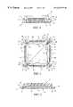
- FIG. 1is a side view of a quad flat package with a heat sink according to the invention.
- FIG. 2is a bottom plan view of the quad flat package of FIG. 1 .
- FIG. 3is a section view taken along lines 3 — 3 of FIG. 2 .
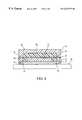
- FIG. 4is a section view taken through a mold for encapsulating a semiconductor circuit on a heat sink to form the quad flat package of FIGS. 1 - 2 .
- the present inventionincludes a heat sink 10 attached to a quad flat package 12 , as illustrated in FIGS. 1-3.
- a plurality of leads 14extend outwardly and downwardly from the quad flat package 12 to connect the package 12 to a circuit board (not shown) or the like.
- the heat sink 10includes a generally square plate 16 defined by sides 16 a , 16 b , 16 c , 16 d , a top surface 18 (FIG. 1 ), a bottom surface 20 , a plurality of bumper hangers 24 and a plurality of bumper heads 26 .
- Each side 16 a , 16 b , 16 c , 16 dincludes a trapezoidal notch 17 .
- the heat sink 10is stamped from a sheet of heat conductive material, but other manufacturing methods and materials can be used.
- Each bumper hanger 24includes a proximal end 28 , attached to a corner of the plate 16 , and a distal end 30 attached to a bumper head 26 .
- Each bumper hanger 24advantageously includes a v-shaped notch 34 , illustrated in FIGS. 2-3, formed in the bottom surface 20 at the distal end of the bumper hanger 24 and extending partially through the plate 16 toward the top surface 18 .
- the notches 34allow the bumper heads 26 to be easily removed by bending when the quad flat package 12 is to be installed on a circuit board to provide additional space on the board for other components.
- Each bumper head 26each includes a distal edge 36 , oriented perpendicular to the diagonal, side edges 37 , 38 , 39 , 40 , and a central aperture 44 .
- Each side edge 38 , 40is oriented parallel to one of the plate sides 16 a , 16 b , 16 c , 16 d and lies beyond the farthest extent of the leads 14 , as illustrated in FIG. 1 .
- the central apertures 44can be used to align the heat sink with a mounting structure for a mold cavity during the encapsulation process and/or with a test fixture for testing the completed quad package.
- the heat sink 10is disposed on a mounting substrate 50 .
- a plurality of alignment pins 52are formed on the substrate 50 and positioned to engage the apertures 44 to accurately position the heat sink 10 with respect to the substrate 50 .
- a semiconductor device 54with a lead frame 56 attached, is positioned in thermal contact with the heat sink 10 , and a mold fixture 60 , including upper and lower mold halves 62 , 64 that define a mold cavity 68 , is positioned to locate the semiconductor device 54 and portions of the lead frame 56 in the mold cavity 68 .
- Encapsulant material 72is introduced into the mold cavity 68 to encapsulate the semiconductor device 54 and portions of the lead frame 56 to form a quad flat package 12 .
- the upper and lower mold halves 62 , 64are removed and the quad flat package 12 is moved to a test fixture (not shown). Again, pins can be formed on the test fixture to engage the apertures 44 to align the quad flat package 12 with the test fixture.
- the bumper heads 26can be broken off from the heat sink 10 by bending them at the v-shaped notch 34 , and the quad flat package 12 is installed on a circuit board (not shown).
- the present inventionprovides an improved quad flat package that takes up less space on a circuit board and has alignment features to facilitate aligning the package with a mounting substrate and/or a test fixture.
Landscapes
- Engineering & Computer Science (AREA)
- Chemical & Material Sciences (AREA)
- Materials Engineering (AREA)
- Physics & Mathematics (AREA)
- Condensed Matter Physics & Semiconductors (AREA)
- General Physics & Mathematics (AREA)
- Computer Hardware Design (AREA)
- Microelectronics & Electronic Packaging (AREA)
- Power Engineering (AREA)
- Cooling Or The Like Of Semiconductors Or Solid State Devices (AREA)
- Lead Frames For Integrated Circuits (AREA)
Abstract
Description
1. Field of the Invention
The present invention relates to integrated circuit quad flat packages and particularly to quad flat packages that include a heat sink with bumpers. More particularly, the invention relates to quad flat packages with removable heat sink bumpers.
2. Description of the Related Art
Quad flat integrated circuit packages are known in the art. Moreover, it is known to attach heat sinks with bumpers to the quad flat packages. For example, U.S. Pat. No. 5,808,359 to Muto et al. discloses a quad flat package that includes a heat-radiating metal plate having bumpers formed at the four corners thereof as a unitary structure. Typically, the bumpers on a quad flat package remain with the package to protect the package leads from damage during handling.
Unfortunately, in conventional quad flat packages, the bumpers take up critical space on a circuit board to which the quad flat package is mounted. The space used by the bumpers could be better used by other components or to reduce the size of the board.
The present invention overcomes the above-recited disadvantage by providing a quad flat package having removable heat sink bumpers. According to the invention, a heat sink for a quad flat package comprises a heat-radiating plate and a plurality of removable bumpers attached to the plate. An area of reduced thickness is disposed at the junction between each bumper and the plate to facilitate removal of the plurality of bumpers from the plate. Preferably, each bumper includes an alignment feature for engaging a complementary feature formed on one of a mounting substrate and a test fixture.
According to one aspect of the invention, the plate is generally square and the plurality of bumpers includes a plurality of bumper hangers and a bumper head coupled to each bumper hanger. The bumper hangers are attached to the plate and extends outwardly from the plate along a diagonal of the plate. The bumper heads include an alignment feature. In a preferred embodiment of the invention, the plurality of bumpers includes four bumpers, with one bumper attached to each corner of the plate and extending outwardly along a diagonal of the plate. The alignment feature preferably includes an aperture formed in each bumper head.
FIG. 1 is a side view of a quad flat package with a heat sink according to the invention.
FIG. 2 is a bottom plan view of the quad flat package of FIG.1.
FIG. 3 is a section view taken alonglines 3—3 of FIG.2.
FIG. 4 is a section view taken through a mold for encapsulating a semiconductor circuit on a heat sink to form the quad flat package of FIGS.1-2.
The present invention includes aheat sink 10 attached to a quadflat package 12, as illustrated in FIGS. 1-3. A plurality ofleads 14 extend outwardly and downwardly from the quadflat package 12 to connect thepackage 12 to a circuit board (not shown) or the like.
As best seen in FIG. 2, theheat sink 10 includes a generallysquare plate 16 defined bysides bottom surface 20, a plurality ofbumper hangers 24 and a plurality ofbumper heads 26. Eachside trapezoidal notch 17. Preferably, theheat sink 10 is stamped from a sheet of heat conductive material, but other manufacturing methods and materials can be used.
Eachbumper hanger 24 includes aproximal end 28, attached to a corner of theplate 16, and adistal end 30 attached to abumper head 26. Eachbumper hanger 24 advantageously includes a v-shaped notch 34, illustrated in FIGS. 2-3, formed in thebottom surface 20 at the distal end of thebumper hanger 24 and extending partially through theplate 16 toward thetop surface 18. Thenotches 34 allow thebumper heads 26 to be easily removed by bending when the quadflat package 12 is to be installed on a circuit board to provide additional space on the board for other components.
Eachbumper head 26 each includes adistal edge 36, oriented perpendicular to the diagonal,side edges central aperture 44. Eachside edge plate sides leads 14, as illustrated in FIG.1. Advantageously, thecentral apertures 44 can be used to align the heat sink with a mounting structure for a mold cavity during the encapsulation process and/or with a test fixture for testing the completed quad package.
As illustrated in FIG. 4, during fabrication of the quad flat package theheat sink 10 is disposed on amounting substrate 50. Preferably, a plurality ofalignment pins 52 are formed on thesubstrate 50 and positioned to engage theapertures 44 to accurately position theheat sink 10 with respect to thesubstrate 50. Asemiconductor device 54, with alead frame 56 attached, is positioned in thermal contact with theheat sink 10, and amold fixture 60, including upper andlower mold halves mold cavity 68, is positioned to locate thesemiconductor device 54 and portions of thelead frame 56 in themold cavity 68. Encapsulant material72 is introduced into themold cavity 68 to encapsulate thesemiconductor device 54 and portions of thelead frame 56 to form a quadflat package 12. After the quadflat package 12 is encapsulated, the upper andlower mold halves flat package 12 is moved to a test fixture (not shown). Again, pins can be formed on the test fixture to engage theapertures 44 to align the quadflat package 12 with the test fixture. After the testing is completed, thebumper heads 26 can be broken off from theheat sink 10 by bending them at the v-shaped notch 34, and the quadflat package 12 is installed on a circuit board (not shown).
The present invention provides an improved quad flat package that takes up less space on a circuit board and has alignment features to facilitate aligning the package with a mounting substrate and/or a test fixture. Modifications can be made to the invention and equivalents substituted for described and illustrated structures without departing from the spirit or scope of the invention. Accordingly, the scope of the present invention is not to be considered as limited by the specifics of the particular structure which have been described and illustrated, but is only limited by the scope of the appended claims.
Claims (26)
1. A heat sink for a semiconductor package comprising:
a heat-radiating plate; and
at least one bumper attached to said plate, said at least one bumper comprising an area of reduced thickness to facilitate removal of said at least one bumper from said plate at said area of reduced thickness.
2. The heat sink of claim1, wherein said at least one bumper includes an alignment feature for engaging a complementary feature formed on a mounting structure.
3. The heat sink of claim1, wherein
said at least one bumper comprises a bumper hanger extending from said plate and a bumper head coupled to said bumper hanger, said bumper head including an alignment feature, and said bumper hanger including said area of reduced thickness to facilitate removal of said bumper head from said bumper hanger.
4. The heat sink of claim3 wherein said at least one bumper is attached to a corner of said plate and extends outwardly along a diagonal of said plate.
5. A heat sink for a semiconductor package comprising:
a heat-radiating plate; and
a plurality of bumpers extending from said plate, each bumper including an alignment feature for engaging a complementary alignment feature formed on a mounting structure, said plurality of bumpers each comprising an area of reduced thickness to facilitate removal of said bumpers from said plate at said areas of reduced thickness.
6. The heat sink of claim5 wherein each alignment feature includes an aperture for engaging an alignment pin formed on said mounting device.
7. The heat sink of claim5 further comprising an encapsulating material covering at least a part of a surface of said plate and wherein at least a portion of an opposing surface of said plate is not covered by said encapsulating material and wherein at least some area of said plurality of bumpers extends past said encapsulating material, said plurality of bumpers each comprising an area of reduced thickness to facilitate removal of said bumpers from said plate at said area of reduced thickness.
8. The heat sink of claim7 wherein said encapsulating material covers a first surface of said plate and extends to about the edges of said plate to form an encapsulating layer and said plurality of bumpers each comprise a bumper hanger extending outwardly from a corner of said plate and a bumper head attached to said bumper hanger, said areas of reduced thickness being located at about the boundary between a said bumper head and a said bumper hanger.
9. A integrated circuit package comprising:
an integrated circuit;
a heat sink thermally coupled with said integrated circuit, the heat sink comprising a plate and a plurality of bumpers extending from said plate, each bumper including an area of reduced thickness to facilitate removal of each said bumper from said plate at said area of reduced thickness; and
an encapsulating layer covering said integrated circuit and bonding it to a portion of said heat sink which does not include an area of each bumper beyond said area of reduced thickness.
10. The integrated circuit package of claim9, wherein the plurality of bumpers include a plurality of respective alignment features for engaging complementary alignment features formed on a mounting structure.
11. The integrated circuit package of claim10, wherein the plurality of alignment features includes an aperture formed in each bumper.
12. The integrated circuit package of claim9 wherein the plate is generally square and the package includes a generally square encapsulating member, the plate further including a plurality of corners and each bumper including a bumper hanger and a bumper head, one bumper hanger extending outwardly from each corner of the plate to a corresponding corner of the encapsulating member, the area of reduced thickness being located at the corner of the encapsulating member.
13. A method for forming a semiconductor package comprising the steps of:
forming a heat sink having a plate portion and a plurality of bumpers, said bumpers extending from said plate portion and said bumpers each comprising an area of reduced thickness to facilitate removal of said bumpers from said plate at said areas of reduced thickness, the plate portion being configured to receive an encapsulation layer;
thermal coupling an integrated circuit with said heat sink; and
encapsulating said integrated circuit with an encapsulating material such that said encapsulating material is in contact with a portion of said heat sink which does not include any part of said bumpers which extend beyond said reduced thickness areas and does not cover an opposing surface of said heat sink.
14. The method of claim13 wherein the step of forming a heat sink includes the step of forming an alignment feature in each bumper.
15. The method of claim14 wherein the alignment feature includes an aperture for receiving an alignment pin.
16. A method for forming a semiconductor package comprising the steps of:
forming a heat sink having a plate portion and a plurality of bumpers extending from said plate portion, wherein each of said bumpers comprises an area of reduced thickness to facilitate removal of said bumpers from said plate at said areas of reduced thickness;
encapsulating a semiconductor die; and
securing the encapsulated die to said heat sink.
17. The method of claim16 wherein each of said bumpers comprise a bumper hanger attached to said plate and a bumper head coupled to said bumper hanger.
18. The method of claim17 further comprising the step of forming an aperture in said bumper head.
19. The method of claim16 wherein the encapsulation of said semiconductor die secures said encapsulated die to said heat sink.
20. The heat sink of claim3 wherein said alignment feature includes an aperture.
21. The method of claim16 further comprising removing said plurality of bumpers from said plate after said semiconductor die is encapsulated.
22. The method of claim18 further comprising detaching each of said bumper heads from said plate at said areas of reduced thickness of said bumpers.
23. The heat sink of claim3 wherein the plurality of bumpers comprises four bumpers.
24. The heat sink of claim3 wherein the plurality of bumpers includes four bumpers and wherein each one of said bumpers is attached to a respective corner of said plate and extends outwardly from said respective corner.
25. The heat sink of claim23 wherein said alignment feature includes an aperture.
26. The heat sink of claim7 wherein each bumper includes a bumper hanger extending outwardly from said plate and a bumper head attached to said bumper hanger, said area of reduced thickness being located at approximately the junction between said bumper head and said bumper hanger.
Priority Applications (2)
| Application Number | Priority Date | Filing Date | Title |
|---|---|---|---|
| US09/247,330US6252772B1 (en) | 1999-02-10 | 1999-02-10 | Removable heat sink bumpers on a quad flat package |
| US09/846,357US6349034B2 (en) | 1999-02-10 | 2001-05-02 | Removable heat sink bumpers on a quad flat package |
Applications Claiming Priority (1)
| Application Number | Priority Date | Filing Date | Title |
|---|---|---|---|
| US09/247,330US6252772B1 (en) | 1999-02-10 | 1999-02-10 | Removable heat sink bumpers on a quad flat package |
Related Child Applications (1)
| Application Number | Title | Priority Date | Filing Date |
|---|---|---|---|
| US09/846,357ContinuationUS6349034B2 (en) | 1999-02-10 | 2001-05-02 | Removable heat sink bumpers on a quad flat package |
Publications (1)
| Publication Number | Publication Date |
|---|---|
| US6252772B1true US6252772B1 (en) | 2001-06-26 |
Family
ID=22934505
Family Applications (2)
| Application Number | Title | Priority Date | Filing Date |
|---|---|---|---|
| US09/247,330Expired - LifetimeUS6252772B1 (en) | 1999-02-10 | 1999-02-10 | Removable heat sink bumpers on a quad flat package |
| US09/846,357Expired - Fee RelatedUS6349034B2 (en) | 1999-02-10 | 2001-05-02 | Removable heat sink bumpers on a quad flat package |
Family Applications After (1)
| Application Number | Title | Priority Date | Filing Date |
|---|---|---|---|
| US09/846,357Expired - Fee RelatedUS6349034B2 (en) | 1999-02-10 | 2001-05-02 | Removable heat sink bumpers on a quad flat package |
Country Status (1)
| Country | Link |
|---|---|
| US (2) | US6252772B1 (en) |
Cited By (23)
| Publication number | Priority date | Publication date | Assignee | Title |
|---|---|---|---|---|
| US6512674B1 (en)* | 1999-07-26 | 2003-01-28 | Nec Corporation | Package for semiconductor device having radiating substrate and radiator fin |
| US6564979B2 (en) | 2001-07-18 | 2003-05-20 | Micron Technology, Inc. | Method and apparatus for dispensing adhesive on microelectronic substrate supports |
| US6614092B2 (en) | 2000-08-16 | 2003-09-02 | Micron Technology, Inc. | Microelectronic device package with conductive elements and associated method of manufacture |
| US6638595B2 (en) | 2000-06-28 | 2003-10-28 | Micron Technology, Inc. | Method and apparatus for reduced flash encapsulation of microelectronic devices |
| US6670719B2 (en) | 1999-08-25 | 2003-12-30 | Micron Technology, Inc. | Microelectronic device package filled with liquid or pressurized gas and associated method of manufacture |
| US6673649B1 (en) | 2002-07-05 | 2004-01-06 | Micron Technology, Inc. | Microelectronic device packages and methods for controlling the disposition of non-conductive materials in such packages |
| US20040113385A1 (en)* | 2002-11-28 | 2004-06-17 | Shimano, Inc. | Bicycle electronic control device with a reset function |
| US20040155331A1 (en)* | 2003-02-11 | 2004-08-12 | Blaine Thurgood | Packaged microelectronic devices and methods for packaging microelectronic devices |
| US20050012185A1 (en)* | 2003-03-04 | 2005-01-20 | Peng Neo Chee | Microelectronic component assemblies employing lead frames having reduced-thickness inner lengths |
| US20050083648A1 (en)* | 2003-10-16 | 2005-04-21 | Janzen Jeffery W. | Methods and apparatuses for transferring heat from microelectronic device modules |
| US20050134299A1 (en)* | 2003-12-22 | 2005-06-23 | Cram Daniel P. | System and apparatus for testing packaged devices and related methods |
| US20060017177A1 (en)* | 2004-07-23 | 2006-01-26 | Seng Eric T S | Microelectronic component assemblies with recessed wire bonds and methods of making same |
| US20060044773A1 (en)* | 2004-08-25 | 2006-03-02 | Micron Technology, Inc. | Methods and apparatuses for transferring heat from stacked microfeature devices |
| US20070031998A1 (en)* | 2000-08-16 | 2007-02-08 | Micron Technology, Inc. | Method and apparatus for removing encapsulating material from a packaged microelectronic device |
| US20070045875A1 (en)* | 2005-08-30 | 2007-03-01 | Micron Technology, Inc. | Methods for wafer-level packaging of microfeature devices and microfeature devices formed using such methods |
| US20070148820A1 (en)* | 2005-12-22 | 2007-06-28 | Micron Technology, Inc. | Microelectronic devices and methods for manufacturing microelectronic devices |
| US20080006940A1 (en)* | 2006-07-05 | 2008-01-10 | Micron Technology, Inc. | Lead frames, microelectronic devices with lead frames, and methods for manufacturing lead frames and microelectronic devices with lead frames |
| US20080224291A1 (en)* | 2007-03-13 | 2008-09-18 | Micron Technology, Inc. | Packaged semiconductor components having substantially rigid support members and methods of packaging semiconductor components |
| US20090026600A1 (en)* | 2007-07-24 | 2009-01-29 | Micron Technology, Inc. | Microelectronic die packages with metal leads, including metal leads for stacked die packages, and associated systems and methods |
| US20090045489A1 (en)* | 2007-08-16 | 2009-02-19 | Micron Technology, Inc. | Microelectronic die packages with leadframes, including leadframe-based interposer for stacked die packages, and associated systems and methods |
| US20090273359A1 (en)* | 2008-05-02 | 2009-11-05 | Micron Technology, Inc. | Electrical testing apparatus having masked sockets and associated systems and methods |
| US7692931B2 (en) | 2006-07-17 | 2010-04-06 | Micron Technology, Inc. | Microelectronic packages with leadframes, including leadframes configured for stacked die packages, and associated systems and methods |
| TWI765161B (en)* | 2016-11-11 | 2022-05-21 | 日商京瓷股份有限公司 | Electrical component mounting package, array type package, and electrical device |
Families Citing this family (3)
| Publication number | Priority date | Publication date | Assignee | Title |
|---|---|---|---|---|
| JP2003110082A (en)* | 2001-09-28 | 2003-04-11 | Mitsubishi Electric Corp | Lead frame, semiconductor device, and method of checking mounting position of semiconductor chip |
| US8693200B2 (en) | 2012-02-07 | 2014-04-08 | International Business Machines Corporation | Semiconductor device cooling module |
| JP6134117B2 (en)* | 2012-10-01 | 2017-05-24 | 株式会社ニコン | Hollow package container |
Citations (14)
| Publication number | Priority date | Publication date | Assignee | Title |
|---|---|---|---|---|
| US4451973A (en)* | 1981-04-28 | 1984-06-05 | Matsushita Electronics Corporation | Method for manufacturing a plastic encapsulated semiconductor device and a lead frame therefor |
| US5067006A (en)* | 1989-08-28 | 1991-11-19 | Sumitomo Electric Industries, Ltd. | Semiconductor device |
| US5367433A (en) | 1993-09-27 | 1994-11-22 | Blomquist Michael L | Package clip on heat sink |
| US5615735A (en) | 1994-09-29 | 1997-04-01 | Hewlett-Packard Co. | Heat sink spring clamp |
| US5660758A (en) | 1995-07-24 | 1997-08-26 | Chip Coolers, Inc. | Mold apparatus for manufacturing a plastic article with interrupted interior threads for securing a heat sink to a heat generating member |
| US5757075A (en) | 1995-04-26 | 1998-05-26 | Sharp Kabushiki Kaisha | Semiconductor heat sink apparatus |
| US5789270A (en) | 1996-01-30 | 1998-08-04 | Industrial Technology Research Institute | Method for assembling a heat sink to a die paddle |
| US5793613A (en) | 1995-12-29 | 1998-08-11 | Sgs-Thomson Microelectronics S.R.1. | Heat-dissipating and supporting structure for a plastic package with a fully insulated heat sink for an electronic device |
| US5798570A (en) | 1996-06-28 | 1998-08-25 | Kabushiki Kaisha Gotoh Seisakusho | Plastic molded semiconductor package with thermal dissipation means |
| US5805430A (en) | 1996-07-22 | 1998-09-08 | International Business Machines Corporation | Zero force heat sink |
| US5808359A (en) | 1994-10-28 | 1998-09-15 | Hitachi, Ltd | Semiconductor device having a heat sink with bumpers for protecting outer leads |
| US5807768A (en) | 1995-09-04 | 1998-09-15 | Anam Industrial Co., Ltd. | Method for fabricating a heat sink-integrated semiconductor package |
| US5815921A (en) | 1994-01-26 | 1998-10-06 | Sun Microsystems, Inc. | Electronic package cooling system and heat sink with heat transfer assembly |
| US5833472A (en) | 1995-07-27 | 1998-11-10 | The Whitaker Corporation | Socket assembly for an electronic package |
Family Cites Families (1)
| Publication number | Priority date | Publication date | Assignee | Title |
|---|---|---|---|---|
| US4399610A (en)* | 1981-04-01 | 1983-08-23 | Western Electric Company, Inc. | Assembling an electronic device |
- 1999
- 1999-02-10USUS09/247,330patent/US6252772B1/ennot_activeExpired - Lifetime
- 2001
- 2001-05-02USUS09/846,357patent/US6349034B2/ennot_activeExpired - Fee Related
Patent Citations (15)
| Publication number | Priority date | Publication date | Assignee | Title |
|---|---|---|---|---|
| US4451973A (en)* | 1981-04-28 | 1984-06-05 | Matsushita Electronics Corporation | Method for manufacturing a plastic encapsulated semiconductor device and a lead frame therefor |
| US5067006A (en)* | 1989-08-28 | 1991-11-19 | Sumitomo Electric Industries, Ltd. | Semiconductor device |
| US5367433A (en) | 1993-09-27 | 1994-11-22 | Blomquist Michael L | Package clip on heat sink |
| US5815921A (en) | 1994-01-26 | 1998-10-06 | Sun Microsystems, Inc. | Electronic package cooling system and heat sink with heat transfer assembly |
| US5615735A (en) | 1994-09-29 | 1997-04-01 | Hewlett-Packard Co. | Heat sink spring clamp |
| US5808359A (en) | 1994-10-28 | 1998-09-15 | Hitachi, Ltd | Semiconductor device having a heat sink with bumpers for protecting outer leads |
| US5757075A (en) | 1995-04-26 | 1998-05-26 | Sharp Kabushiki Kaisha | Semiconductor heat sink apparatus |
| US5667870A (en) | 1995-07-24 | 1997-09-16 | Chip Coolers, Inc. | Plastic article with interrupted interior threads for securing a threaded heat sink to a heat generating member |
| US5660758A (en) | 1995-07-24 | 1997-08-26 | Chip Coolers, Inc. | Mold apparatus for manufacturing a plastic article with interrupted interior threads for securing a heat sink to a heat generating member |
| US5833472A (en) | 1995-07-27 | 1998-11-10 | The Whitaker Corporation | Socket assembly for an electronic package |
| US5807768A (en) | 1995-09-04 | 1998-09-15 | Anam Industrial Co., Ltd. | Method for fabricating a heat sink-integrated semiconductor package |
| US5793613A (en) | 1995-12-29 | 1998-08-11 | Sgs-Thomson Microelectronics S.R.1. | Heat-dissipating and supporting structure for a plastic package with a fully insulated heat sink for an electronic device |
| US5789270A (en) | 1996-01-30 | 1998-08-04 | Industrial Technology Research Institute | Method for assembling a heat sink to a die paddle |
| US5798570A (en) | 1996-06-28 | 1998-08-25 | Kabushiki Kaisha Gotoh Seisakusho | Plastic molded semiconductor package with thermal dissipation means |
| US5805430A (en) | 1996-07-22 | 1998-09-08 | International Business Machines Corporation | Zero force heat sink |
Cited By (70)
| Publication number | Priority date | Publication date | Assignee | Title |
|---|---|---|---|---|
| US6512674B1 (en)* | 1999-07-26 | 2003-01-28 | Nec Corporation | Package for semiconductor device having radiating substrate and radiator fin |
| US6670719B2 (en) | 1999-08-25 | 2003-12-30 | Micron Technology, Inc. | Microelectronic device package filled with liquid or pressurized gas and associated method of manufacture |
| US6909171B2 (en) | 1999-08-25 | 2005-06-21 | Micron Technology, Inc. | Microelectronic device package filled with liquid or pressurized gas and associated method of manufacture |
| US6638595B2 (en) | 2000-06-28 | 2003-10-28 | Micron Technology, Inc. | Method and apparatus for reduced flash encapsulation of microelectronic devices |
| US6644949B2 (en) | 2000-06-28 | 2003-11-11 | Micron Technology, Inc. | Apparatus for reduced flash encapsulation of microelectronic devices |
| US6614092B2 (en) | 2000-08-16 | 2003-09-02 | Micron Technology, Inc. | Microelectronic device package with conductive elements and associated method of manufacture |
| US20070031998A1 (en)* | 2000-08-16 | 2007-02-08 | Micron Technology, Inc. | Method and apparatus for removing encapsulating material from a packaged microelectronic device |
| US6709968B1 (en) | 2000-08-16 | 2004-03-23 | Micron Technology, Inc. | Microelectronic device with package with conductive elements and associated method of manufacture |
| US7273769B1 (en) | 2000-08-16 | 2007-09-25 | Micron Technology, Inc. | Method and apparatus for removing encapsulating material from a packaged microelectronic device |
| US7405487B2 (en) | 2000-08-16 | 2008-07-29 | Micron Technology, Inc. | Method and apparatus for removing encapsulating material from a packaged microelectronic device |
| US6564979B2 (en) | 2001-07-18 | 2003-05-20 | Micron Technology, Inc. | Method and apparatus for dispensing adhesive on microelectronic substrate supports |
| US20040101991A1 (en)* | 2002-07-05 | 2004-05-27 | Hiatt William Mark | Microelectronic device packages and methods for controlling the disposition of non-conductive materials in such packages |
| US7470563B2 (en) | 2002-07-05 | 2008-12-30 | Micron Technology, Inc. | Microelectronic device packages and methods for controlling the disposition of non-conductive materials in such packages |
| US20060057774A1 (en)* | 2002-07-05 | 2006-03-16 | Hiatt William M | Microelectronic device packages and methods for controlling the disposition of non-conductive materials in such packages |
| US6673649B1 (en) | 2002-07-05 | 2004-01-06 | Micron Technology, Inc. | Microelectronic device packages and methods for controlling the disposition of non-conductive materials in such packages |
| US7087995B2 (en) | 2002-07-05 | 2006-08-08 | Micron Technology, Inc. | Microelectronic device packages and methods for controlling the disposition of non-conductive materials in such packages |
| US20040113385A1 (en)* | 2002-11-28 | 2004-06-17 | Shimano, Inc. | Bicycle electronic control device with a reset function |
| US6879050B2 (en) | 2003-02-11 | 2005-04-12 | Micron Technology, Inc. | Packaged microelectronic devices and methods for packaging microelectronic devices |
| US20040155331A1 (en)* | 2003-02-11 | 2004-08-12 | Blaine Thurgood | Packaged microelectronic devices and methods for packaging microelectronic devices |
| US20050012185A1 (en)* | 2003-03-04 | 2005-01-20 | Peng Neo Chee | Microelectronic component assemblies employing lead frames having reduced-thickness inner lengths |
| US7691680B2 (en) | 2003-03-04 | 2010-04-06 | Micron Technologies, Inc. | Method of fabricating microelectronic component assemblies employing lead frames having reduced-thickness inner lengths |
| US7425470B2 (en) | 2003-03-04 | 2008-09-16 | Micron Technology, Inc. | Microelectronic component assemblies employing lead frames having reduced-thickness inner lengths |
| US20050083648A1 (en)* | 2003-10-16 | 2005-04-21 | Janzen Jeffery W. | Methods and apparatuses for transferring heat from microelectronic device modules |
| US6888719B1 (en) | 2003-10-16 | 2005-05-03 | Micron Technology, Inc. | Methods and apparatuses for transferring heat from microelectronic device modules |
| US7043388B2 (en) | 2003-12-22 | 2006-05-09 | Micron Technology, Inc. | System and apparatus for testing packaged devices and related methods |
| US20050134299A1 (en)* | 2003-12-22 | 2005-06-23 | Cram Daniel P. | System and apparatus for testing packaged devices and related methods |
| US7250328B2 (en) | 2004-07-23 | 2007-07-31 | Micron Technology, Inc. | Microelectronic component assemblies with recessed wire bonds and methods of making same |
| US20060017177A1 (en)* | 2004-07-23 | 2006-01-26 | Seng Eric T S | Microelectronic component assemblies with recessed wire bonds and methods of making same |
| US7696003B2 (en) | 2004-07-23 | 2010-04-13 | Micron Technology, Inc. | Microelectronic component assemblies with recessed wire bonds and methods of making same |
| US7365424B2 (en) | 2004-07-23 | 2008-04-29 | Micron Technology, Inc. | Microelectronic component assemblies with recessed wire bonds and methods of making same |
| US20080164591A1 (en)* | 2004-07-23 | 2008-07-10 | Micron Technology, Inc. | Microelectronic component assemblies with recessed wire bonds and methods of making same |
| US20060208366A1 (en)* | 2004-07-23 | 2006-09-21 | Micron Technology, Inc. | Microelectronic component assemblies with recessed wire bonds and methods of making same |
| US20090321061A1 (en)* | 2004-08-25 | 2009-12-31 | Micron Technology, Inc. | Methods and apparatuses for transferring heat from stacked microfeature devices |
| US9960148B2 (en) | 2004-08-25 | 2018-05-01 | Micron Technology, Inc. | Methods for transferring heat from stacked microfeature devices |
| US7602618B2 (en) | 2004-08-25 | 2009-10-13 | Micron Technology, Inc. | Methods and apparatuses for transferring heat from stacked microfeature devices |
| US8111515B2 (en) | 2004-08-25 | 2012-02-07 | Micron Technology, Inc. | Methods and apparatuses for transferring heat from stacked microfeature devices |
| US20060044773A1 (en)* | 2004-08-25 | 2006-03-02 | Micron Technology, Inc. | Methods and apparatuses for transferring heat from stacked microfeature devices |
| US20070045875A1 (en)* | 2005-08-30 | 2007-03-01 | Micron Technology, Inc. | Methods for wafer-level packaging of microfeature devices and microfeature devices formed using such methods |
| US20100327462A1 (en)* | 2005-08-30 | 2010-12-30 | Micron Technology, Inc. | Methods for wafer-level packaging of microfeature devices and microfeature devices formed using such methods |
| US7807505B2 (en) | 2005-08-30 | 2010-10-05 | Micron Technology, Inc. | Methods for wafer-level packaging of microfeature devices and microfeature devices formed using such methods |
| US8704380B2 (en) | 2005-08-30 | 2014-04-22 | Micron Technology, Inc. | Methods for wafer-level packaging of microfeature devices and microfeature devices formed using such methods |
| US20070148820A1 (en)* | 2005-12-22 | 2007-06-28 | Micron Technology, Inc. | Microelectronic devices and methods for manufacturing microelectronic devices |
| US20080006940A1 (en)* | 2006-07-05 | 2008-01-10 | Micron Technology, Inc. | Lead frames, microelectronic devices with lead frames, and methods for manufacturing lead frames and microelectronic devices with lead frames |
| US7692931B2 (en) | 2006-07-17 | 2010-04-06 | Micron Technology, Inc. | Microelectronic packages with leadframes, including leadframes configured for stacked die packages, and associated systems and methods |
| US20100173454A1 (en)* | 2006-07-17 | 2010-07-08 | Micron Technology, Inc. | Microelectronic packages with leadframes, including leadframes configured for stacked die packages, and associated systems and methods |
| US8869387B2 (en) | 2006-07-17 | 2014-10-28 | Micron Technology, Inc. | Methods for making microelectronic die systems |
| US20080224291A1 (en)* | 2007-03-13 | 2008-09-18 | Micron Technology, Inc. | Packaged semiconductor components having substantially rigid support members and methods of packaging semiconductor components |
| US7750449B2 (en) | 2007-03-13 | 2010-07-06 | Micron Technology, Inc. | Packaged semiconductor components having substantially rigid support members and methods of packaging semiconductor components |
| US10763185B2 (en) | 2007-03-13 | 2020-09-01 | Micron Technology, Inc. | Packaged semiconductor components having substantially rigid support members |
| US20100255636A1 (en)* | 2007-03-13 | 2010-10-07 | Micron Technology, Inc. | Packaged semiconductor components having substantially rigid support members and methods of packaging semiconductor components |
| US9362208B2 (en) | 2007-03-13 | 2016-06-07 | Micron Technology, Inc. | Packaged semiconductor components having substantially rigid support members and methods of packaging semiconductor components |
| US9960094B2 (en) | 2007-03-13 | 2018-05-01 | Micron Technology, Inc. | Packaged semiconductor components having substantially rigid support members and methods of packaging semiconductor components |
| US10312173B2 (en) | 2007-03-13 | 2019-06-04 | Micron Technology, Inc. | Packaged semiconductor components having substantially rigid support members and methods of packaging semiconductor components |
| US10396059B2 (en) | 2007-07-24 | 2019-08-27 | Micron Technology, Inc. | Microelectronic die packages with metal leads, including metal leads for stacked die packages, and associated systems and methods |
| US8198720B2 (en) | 2007-07-24 | 2012-06-12 | Micron Technology, Inc. | Microelectronic die packages with metal leads, including metal leads for stacked die packages, and associated systems and methods |
| US7843050B2 (en) | 2007-07-24 | 2010-11-30 | Micron Technology, Inc. | Microelectronic die packages with metal leads, including metal leads for stacked die packages, and associated systems and methods |
| US8536702B2 (en) | 2007-07-24 | 2013-09-17 | Micron Technology, Inc. | Microelectronic die packages with metal leads, including metal leads for stacked die packages, and associated systems and methods |
| US10056359B2 (en) | 2007-07-24 | 2018-08-21 | Micron Technology, Inc. | Microelectronic die packages with metal leads, including metal leads for stacked die packages, and associated systems and methods |
| US20090026600A1 (en)* | 2007-07-24 | 2009-01-29 | Micron Technology, Inc. | Microelectronic die packages with metal leads, including metal leads for stacked die packages, and associated systems and methods |
| US8906744B2 (en) | 2007-07-24 | 2014-12-09 | Micron Technology, Inc. | Microelectronic die packages with metal leads, including metal leads for stacked die packages, and associated systems and methods |
| US9165910B2 (en) | 2007-07-24 | 2015-10-20 | Micron Technology, Inc. | Microelectronic die packages with metal leads, including metal leads for stacked die packages, and associated systems and methods |
| US20110068454A1 (en)* | 2007-07-24 | 2011-03-24 | Micron Technology, Inc. | Microelectronic die packages with metal leads, including metal leads for stacked die packages, and associated systems and methods |
| US9653444B2 (en) | 2007-07-24 | 2017-05-16 | Micron Technology, Inc. | Microelectronic die packages with metal leads, including metal leads for stacked die packages, and associated systems and methods |
| US20110215453A1 (en)* | 2007-08-16 | 2011-09-08 | Micron Technology, Inc. | Microelectronic die packages with leadframes, including leadframe-based interposer for stacked die packages, and associated systems and methods |
| US20090045489A1 (en)* | 2007-08-16 | 2009-02-19 | Micron Technology, Inc. | Microelectronic die packages with leadframes, including leadframe-based interposer for stacked die packages, and associated systems and methods |
| US8525320B2 (en) | 2007-08-16 | 2013-09-03 | Micron Technology, Inc. | Microelectronic die packages with leadframes, including leadframe-based interposer for stacked die packages, and associated systems and methods |
| US7947529B2 (en) | 2007-08-16 | 2011-05-24 | Micron Technology, Inc. | Microelectronic die packages with leadframes, including leadframe-based interposer for stacked die packages, and associated systems and methods |
| US20090273359A1 (en)* | 2008-05-02 | 2009-11-05 | Micron Technology, Inc. | Electrical testing apparatus having masked sockets and associated systems and methods |
| US7857646B2 (en) | 2008-05-02 | 2010-12-28 | Micron Technology, Inc. | Electrical testing apparatus having masked sockets and associated systems and methods |
| TWI765161B (en)* | 2016-11-11 | 2022-05-21 | 日商京瓷股份有限公司 | Electrical component mounting package, array type package, and electrical device |
Also Published As
| Publication number | Publication date |
|---|---|
| US20010028553A1 (en) | 2001-10-11 |
| US6349034B2 (en) | 2002-02-19 |
Similar Documents
| Publication | Publication Date | Title |
|---|---|---|
| US6252772B1 (en) | Removable heat sink bumpers on a quad flat package | |
| US5105259A (en) | Thermally enhanced semiconductor device utilizing a vacuum to ultimately enhance thermal dissipation | |
| US5147821A (en) | Method for making a thermally enhanced semiconductor device by holding a leadframe against a heatsink through vacuum suction in a molding operation | |
| US6611047B2 (en) | Semiconductor package with singulation crease | |
| EP0232837B1 (en) | Plastic molded chip carrier package and method of fabricating the same | |
| US6452255B1 (en) | Low inductance leadless package | |
| US5986333A (en) | Semiconductor apparatus and method for fabricating the same | |
| KR100927319B1 (en) | Stamped Leadframe and Manufacturing Method Thereof | |
| US5256598A (en) | Shrink accommodating lead frame | |
| EP2577726B1 (en) | Stacked interposer leadframes | |
| US6448107B1 (en) | Pin indicator for leadless leadframe packages | |
| US6677665B2 (en) | Dual-die integrated circuit package | |
| US20090008754A1 (en) | Resin-sealed semiconductor device, leadframe with die pads, and manufacturing method for leadframe with die pads | |
| US5963796A (en) | Fabrication method for semiconductor package substrate and semiconductor package | |
| JPH06505126A (en) | Carrier ring for semiconductor packages | |
| US7863730B2 (en) | Array-molded package heat spreader and fabrication method therefor | |
| US6686652B1 (en) | Locking lead tips and die attach pad for a leadless package apparatus and method | |
| US20180211907A1 (en) | Semiconductor package with heat slug and rivet free die attach area | |
| US5886396A (en) | Leadframe assembly for conducting thermal energy from a semiconductor die disposed in a package | |
| US5036381A (en) | Multiple electronic devices within a single carrier structure | |
| US20080157297A1 (en) | Stress-Resistant Leadframe and Method | |
| US10381293B2 (en) | Integrated circuit package having an IC die between top and bottom leadframes | |
| KR100940760B1 (en) | Semiconductor package | |
| US20020089041A1 (en) | Lead-frame design modification to facilitate removal of resist tape from the lead-frame | |
| JP2503360Y2 (en) | Resin-sealed semiconductor integrated circuit device |
Legal Events
| Date | Code | Title | Description |
|---|---|---|---|
| AS | Assignment | Owner name:MICRON TECHNOLOGY, INC., IDAHO Free format text:ASSIGNMENT OF ASSIGNORS INTEREST;ASSIGNOR:ALLEN, TIMOTHY J.;REEL/FRAME:009775/0744 Effective date:19990205 | |
| STCF | Information on status: patent grant | Free format text:PATENTED CASE | |
| FPAY | Fee payment | Year of fee payment:4 | |
| FEPP | Fee payment procedure | Free format text:PAYER NUMBER DE-ASSIGNED (ORIGINAL EVENT CODE: RMPN); ENTITY STATUS OF PATENT OWNER: LARGE ENTITY Free format text:PAYOR NUMBER ASSIGNED (ORIGINAL EVENT CODE: ASPN); ENTITY STATUS OF PATENT OWNER: LARGE ENTITY | |
| FPAY | Fee payment | Year of fee payment:8 | |
| FPAY | Fee payment | Year of fee payment:12 |