US6252308B1 - Packaged die PCB with heat sink encapsulant - Google Patents
Packaged die PCB with heat sink encapsulantDownload PDFInfo
- Publication number
- US6252308B1 US6252308B1US09/189,102US18910298AUS6252308B1US 6252308 B1US6252308 B1US 6252308B1US 18910298 AUS18910298 AUS 18910298AUS 6252308 B1US6252308 B1US 6252308B1
- Authority
- US
- United States
- Prior art keywords
- semiconductor chip
- substrate
- semiconductor
- contact point
- electrical contact
- Prior art date
- Legal status (The legal status is an assumption and is not a legal conclusion. Google has not performed a legal analysis and makes no representation as to the accuracy of the status listed.)
- Expired - Lifetime
Links
Images


Classifications
- H—ELECTRICITY
- H01—ELECTRIC ELEMENTS
- H01L—SEMICONDUCTOR DEVICES NOT COVERED BY CLASS H10
- H01L24/00—Arrangements for connecting or disconnecting semiconductor or solid-state bodies; Methods or apparatus related thereto
- H01L24/80—Methods for connecting semiconductor or other solid state bodies using means for bonding being attached to, or being formed on, the surface to be connected
- H01L24/85—Methods for connecting semiconductor or other solid state bodies using means for bonding being attached to, or being formed on, the surface to be connected using a wire connector
- H—ELECTRICITY
- H01—ELECTRIC ELEMENTS
- H01L—SEMICONDUCTOR DEVICES NOT COVERED BY CLASS H10
- H01L21/00—Processes or apparatus adapted for the manufacture or treatment of semiconductor or solid state devices or of parts thereof
- H01L21/02—Manufacture or treatment of semiconductor devices or of parts thereof
- H01L21/04—Manufacture or treatment of semiconductor devices or of parts thereof the devices having potential barriers, e.g. a PN junction, depletion layer or carrier concentration layer
- H01L21/50—Assembly of semiconductor devices using processes or apparatus not provided for in a single one of the groups H01L21/18 - H01L21/326 or H10D48/04 - H10D48/07 e.g. sealing of a cap to a base of a container
- H01L21/56—Encapsulations, e.g. encapsulation layers, coatings
- H01L21/563—Encapsulation of active face of flip-chip device, e.g. underfilling or underencapsulation of flip-chip, encapsulation preform on chip or mounting substrate
- H—ELECTRICITY
- H01—ELECTRIC ELEMENTS
- H01L—SEMICONDUCTOR DEVICES NOT COVERED BY CLASS H10
- H01L23/00—Details of semiconductor or other solid state devices
- H01L23/28—Encapsulations, e.g. encapsulating layers, coatings, e.g. for protection
- H01L23/31—Encapsulations, e.g. encapsulating layers, coatings, e.g. for protection characterised by the arrangement or shape
- H01L23/3107—Encapsulations, e.g. encapsulating layers, coatings, e.g. for protection characterised by the arrangement or shape the device being completely enclosed
- H01L23/3121—Encapsulations, e.g. encapsulating layers, coatings, e.g. for protection characterised by the arrangement or shape the device being completely enclosed a substrate forming part of the encapsulation
- H01L23/3128—Encapsulations, e.g. encapsulating layers, coatings, e.g. for protection characterised by the arrangement or shape the device being completely enclosed a substrate forming part of the encapsulation the substrate having spherical bumps for external connection
- H—ELECTRICITY
- H01—ELECTRIC ELEMENTS
- H01L—SEMICONDUCTOR DEVICES NOT COVERED BY CLASS H10
- H01L23/00—Details of semiconductor or other solid state devices
- H01L23/28—Encapsulations, e.g. encapsulating layers, coatings, e.g. for protection
- H01L23/31—Encapsulations, e.g. encapsulating layers, coatings, e.g. for protection characterised by the arrangement or shape
- H01L23/3107—Encapsulations, e.g. encapsulating layers, coatings, e.g. for protection characterised by the arrangement or shape the device being completely enclosed
- H01L23/3135—Double encapsulation or coating and encapsulation
- H—ELECTRICITY
- H01—ELECTRIC ELEMENTS
- H01L—SEMICONDUCTOR DEVICES NOT COVERED BY CLASS H10
- H01L23/00—Details of semiconductor or other solid state devices
- H01L23/28—Encapsulations, e.g. encapsulating layers, coatings, e.g. for protection
- H01L23/31—Encapsulations, e.g. encapsulating layers, coatings, e.g. for protection characterised by the arrangement or shape
- H01L23/3157—Partial encapsulation or coating
- H—ELECTRICITY
- H01—ELECTRIC ELEMENTS
- H01L—SEMICONDUCTOR DEVICES NOT COVERED BY CLASS H10
- H01L23/00—Details of semiconductor or other solid state devices
- H01L23/34—Arrangements for cooling, heating, ventilating or temperature compensation ; Temperature sensing arrangements
- H01L23/42—Fillings or auxiliary members in containers or encapsulations selected or arranged to facilitate heating or cooling
- H01L23/433—Auxiliary members in containers characterised by their shape, e.g. pistons
- H01L23/4334—Auxiliary members in encapsulations
- H—ELECTRICITY
- H01—ELECTRIC ELEMENTS
- H01L—SEMICONDUCTOR DEVICES NOT COVERED BY CLASS H10
- H01L24/00—Arrangements for connecting or disconnecting semiconductor or solid-state bodies; Methods or apparatus related thereto
- H01L24/01—Means for bonding being attached to, or being formed on, the surface to be connected, e.g. chip-to-package, die-attach, "first-level" interconnects; Manufacturing methods related thereto
- H01L24/26—Layer connectors, e.g. plate connectors, solder or adhesive layers; Manufacturing methods related thereto
- H01L24/31—Structure, shape, material or disposition of the layer connectors after the connecting process
- H01L24/32—Structure, shape, material or disposition of the layer connectors after the connecting process of an individual layer connector
- H—ELECTRICITY
- H01—ELECTRIC ELEMENTS
- H01L—SEMICONDUCTOR DEVICES NOT COVERED BY CLASS H10
- H01L24/00—Arrangements for connecting or disconnecting semiconductor or solid-state bodies; Methods or apparatus related thereto
- H01L24/01—Means for bonding being attached to, or being formed on, the surface to be connected, e.g. chip-to-package, die-attach, "first-level" interconnects; Manufacturing methods related thereto
- H01L24/42—Wire connectors; Manufacturing methods related thereto
- H01L24/47—Structure, shape, material or disposition of the wire connectors after the connecting process
- H01L24/48—Structure, shape, material or disposition of the wire connectors after the connecting process of an individual wire connector
- H—ELECTRICITY
- H01—ELECTRIC ELEMENTS
- H01L—SEMICONDUCTOR DEVICES NOT COVERED BY CLASS H10
- H01L24/00—Arrangements for connecting or disconnecting semiconductor or solid-state bodies; Methods or apparatus related thereto
- H01L24/74—Apparatus for manufacturing arrangements for connecting or disconnecting semiconductor or solid-state bodies
- H01L24/75—Apparatus for connecting with bump connectors or layer connectors
- H—ELECTRICITY
- H01—ELECTRIC ELEMENTS
- H01L—SEMICONDUCTOR DEVICES NOT COVERED BY CLASS H10
- H01L24/00—Arrangements for connecting or disconnecting semiconductor or solid-state bodies; Methods or apparatus related thereto
- H01L24/80—Methods for connecting semiconductor or other solid state bodies using means for bonding being attached to, or being formed on, the surface to be connected
- H01L24/81—Methods for connecting semiconductor or other solid state bodies using means for bonding being attached to, or being formed on, the surface to be connected using a bump connector
- H—ELECTRICITY
- H01—ELECTRIC ELEMENTS
- H01L—SEMICONDUCTOR DEVICES NOT COVERED BY CLASS H10
- H01L24/00—Arrangements for connecting or disconnecting semiconductor or solid-state bodies; Methods or apparatus related thereto
- H01L24/93—Batch processes
- H01L24/95—Batch processes at chip-level, i.e. with connecting carried out on a plurality of singulated devices, i.e. on diced chips
- H01L24/97—Batch processes at chip-level, i.e. with connecting carried out on a plurality of singulated devices, i.e. on diced chips the devices being connected to a common substrate, e.g. interposer, said common substrate being separable into individual assemblies after connecting
- H—ELECTRICITY
- H01—ELECTRIC ELEMENTS
- H01L—SEMICONDUCTOR DEVICES NOT COVERED BY CLASS H10
- H01L25/00—Assemblies consisting of a plurality of semiconductor or other solid state devices
- H01L25/03—Assemblies consisting of a plurality of semiconductor or other solid state devices all the devices being of a type provided for in a single subclass of subclasses H10B, H10D, H10F, H10H, H10K or H10N, e.g. assemblies of rectifier diodes
- H01L25/04—Assemblies consisting of a plurality of semiconductor or other solid state devices all the devices being of a type provided for in a single subclass of subclasses H10B, H10D, H10F, H10H, H10K or H10N, e.g. assemblies of rectifier diodes the devices not having separate containers
- H01L25/065—Assemblies consisting of a plurality of semiconductor or other solid state devices all the devices being of a type provided for in a single subclass of subclasses H10B, H10D, H10F, H10H, H10K or H10N, e.g. assemblies of rectifier diodes the devices not having separate containers the devices being of a type provided for in group H10D89/00
- H01L25/0655—Assemblies consisting of a plurality of semiconductor or other solid state devices all the devices being of a type provided for in a single subclass of subclasses H10B, H10D, H10F, H10H, H10K or H10N, e.g. assemblies of rectifier diodes the devices not having separate containers the devices being of a type provided for in group H10D89/00 the devices being arranged next to each other
- H—ELECTRICITY
- H01—ELECTRIC ELEMENTS
- H01L—SEMICONDUCTOR DEVICES NOT COVERED BY CLASS H10
- H01L2224/00—Indexing scheme for arrangements for connecting or disconnecting semiconductor or solid-state bodies and methods related thereto as covered by H01L24/00
- H01L2224/01—Means for bonding being attached to, or being formed on, the surface to be connected, e.g. chip-to-package, die-attach, "first-level" interconnects; Manufacturing methods related thereto
- H01L2224/02—Bonding areas; Manufacturing methods related thereto
- H01L2224/04—Structure, shape, material or disposition of the bonding areas prior to the connecting process
- H01L2224/0401—Bonding areas specifically adapted for bump connectors, e.g. under bump metallisation [UBM]
- H—ELECTRICITY
- H01—ELECTRIC ELEMENTS
- H01L—SEMICONDUCTOR DEVICES NOT COVERED BY CLASS H10
- H01L2224/00—Indexing scheme for arrangements for connecting or disconnecting semiconductor or solid-state bodies and methods related thereto as covered by H01L24/00
- H01L2224/01—Means for bonding being attached to, or being formed on, the surface to be connected, e.g. chip-to-package, die-attach, "first-level" interconnects; Manufacturing methods related thereto
- H01L2224/02—Bonding areas; Manufacturing methods related thereto
- H01L2224/04—Structure, shape, material or disposition of the bonding areas prior to the connecting process
- H01L2224/05—Structure, shape, material or disposition of the bonding areas prior to the connecting process of an individual bonding area
- H01L2224/0554—External layer
- H01L2224/05599—Material
- H—ELECTRICITY
- H01—ELECTRIC ELEMENTS
- H01L—SEMICONDUCTOR DEVICES NOT COVERED BY CLASS H10
- H01L2224/00—Indexing scheme for arrangements for connecting or disconnecting semiconductor or solid-state bodies and methods related thereto as covered by H01L24/00
- H01L2224/01—Means for bonding being attached to, or being formed on, the surface to be connected, e.g. chip-to-package, die-attach, "first-level" interconnects; Manufacturing methods related thereto
- H01L2224/10—Bump connectors; Manufacturing methods related thereto
- H01L2224/15—Structure, shape, material or disposition of the bump connectors after the connecting process
- H01L2224/16—Structure, shape, material or disposition of the bump connectors after the connecting process of an individual bump connector
- H01L2224/161—Disposition
- H01L2224/16151—Disposition the bump connector connecting between a semiconductor or solid-state body and an item not being a semiconductor or solid-state body, e.g. chip-to-substrate, chip-to-passive
- H01L2224/16221—Disposition the bump connector connecting between a semiconductor or solid-state body and an item not being a semiconductor or solid-state body, e.g. chip-to-substrate, chip-to-passive the body and the item being stacked
- H01L2224/16225—Disposition the bump connector connecting between a semiconductor or solid-state body and an item not being a semiconductor or solid-state body, e.g. chip-to-substrate, chip-to-passive the body and the item being stacked the item being non-metallic, e.g. insulating substrate with or without metallisation
- H—ELECTRICITY
- H01—ELECTRIC ELEMENTS
- H01L—SEMICONDUCTOR DEVICES NOT COVERED BY CLASS H10
- H01L2224/00—Indexing scheme for arrangements for connecting or disconnecting semiconductor or solid-state bodies and methods related thereto as covered by H01L24/00
- H01L2224/01—Means for bonding being attached to, or being formed on, the surface to be connected, e.g. chip-to-package, die-attach, "first-level" interconnects; Manufacturing methods related thereto
- H01L2224/26—Layer connectors, e.g. plate connectors, solder or adhesive layers; Manufacturing methods related thereto
- H01L2224/31—Structure, shape, material or disposition of the layer connectors after the connecting process
- H01L2224/32—Structure, shape, material or disposition of the layer connectors after the connecting process of an individual layer connector
- H01L2224/321—Disposition
- H01L2224/32151—Disposition the layer connector connecting between a semiconductor or solid-state body and an item not being a semiconductor or solid-state body, e.g. chip-to-substrate, chip-to-passive
- H01L2224/32221—Disposition the layer connector connecting between a semiconductor or solid-state body and an item not being a semiconductor or solid-state body, e.g. chip-to-substrate, chip-to-passive the body and the item being stacked
- H01L2224/32225—Disposition the layer connector connecting between a semiconductor or solid-state body and an item not being a semiconductor or solid-state body, e.g. chip-to-substrate, chip-to-passive the body and the item being stacked the item being non-metallic, e.g. insulating substrate with or without metallisation
- H—ELECTRICITY
- H01—ELECTRIC ELEMENTS
- H01L—SEMICONDUCTOR DEVICES NOT COVERED BY CLASS H10
- H01L2224/00—Indexing scheme for arrangements for connecting or disconnecting semiconductor or solid-state bodies and methods related thereto as covered by H01L24/00
- H01L2224/01—Means for bonding being attached to, or being formed on, the surface to be connected, e.g. chip-to-package, die-attach, "first-level" interconnects; Manufacturing methods related thereto
- H01L2224/42—Wire connectors; Manufacturing methods related thereto
- H01L2224/47—Structure, shape, material or disposition of the wire connectors after the connecting process
- H01L2224/48—Structure, shape, material or disposition of the wire connectors after the connecting process of an individual wire connector
- H01L2224/4805—Shape
- H01L2224/4809—Loop shape
- H01L2224/48091—Arched
- H—ELECTRICITY
- H01—ELECTRIC ELEMENTS
- H01L—SEMICONDUCTOR DEVICES NOT COVERED BY CLASS H10
- H01L2224/00—Indexing scheme for arrangements for connecting or disconnecting semiconductor or solid-state bodies and methods related thereto as covered by H01L24/00
- H01L2224/01—Means for bonding being attached to, or being formed on, the surface to be connected, e.g. chip-to-package, die-attach, "first-level" interconnects; Manufacturing methods related thereto
- H01L2224/42—Wire connectors; Manufacturing methods related thereto
- H01L2224/47—Structure, shape, material or disposition of the wire connectors after the connecting process
- H01L2224/48—Structure, shape, material or disposition of the wire connectors after the connecting process of an individual wire connector
- H01L2224/481—Disposition
- H01L2224/48151—Connecting between a semiconductor or solid-state body and an item not being a semiconductor or solid-state body, e.g. chip-to-substrate, chip-to-passive
- H01L2224/48221—Connecting between a semiconductor or solid-state body and an item not being a semiconductor or solid-state body, e.g. chip-to-substrate, chip-to-passive the body and the item being stacked
- H01L2224/48225—Connecting between a semiconductor or solid-state body and an item not being a semiconductor or solid-state body, e.g. chip-to-substrate, chip-to-passive the body and the item being stacked the item being non-metallic, e.g. insulating substrate with or without metallisation
- H01L2224/48227—Connecting between a semiconductor or solid-state body and an item not being a semiconductor or solid-state body, e.g. chip-to-substrate, chip-to-passive the body and the item being stacked the item being non-metallic, e.g. insulating substrate with or without metallisation connecting the wire to a bond pad of the item
- H—ELECTRICITY
- H01—ELECTRIC ELEMENTS
- H01L—SEMICONDUCTOR DEVICES NOT COVERED BY CLASS H10
- H01L2224/00—Indexing scheme for arrangements for connecting or disconnecting semiconductor or solid-state bodies and methods related thereto as covered by H01L24/00
- H01L2224/01—Means for bonding being attached to, or being formed on, the surface to be connected, e.g. chip-to-package, die-attach, "first-level" interconnects; Manufacturing methods related thereto
- H01L2224/42—Wire connectors; Manufacturing methods related thereto
- H01L2224/47—Structure, shape, material or disposition of the wire connectors after the connecting process
- H01L2224/48—Structure, shape, material or disposition of the wire connectors after the connecting process of an individual wire connector
- H01L2224/481—Disposition
- H01L2224/48151—Connecting between a semiconductor or solid-state body and an item not being a semiconductor or solid-state body, e.g. chip-to-substrate, chip-to-passive
- H01L2224/48221—Connecting between a semiconductor or solid-state body and an item not being a semiconductor or solid-state body, e.g. chip-to-substrate, chip-to-passive the body and the item being stacked
- H01L2224/48245—Connecting between a semiconductor or solid-state body and an item not being a semiconductor or solid-state body, e.g. chip-to-substrate, chip-to-passive the body and the item being stacked the item being metallic
- H01L2224/48247—Connecting between a semiconductor or solid-state body and an item not being a semiconductor or solid-state body, e.g. chip-to-substrate, chip-to-passive the body and the item being stacked the item being metallic connecting the wire to a bond pad of the item
- H—ELECTRICITY
- H01—ELECTRIC ELEMENTS
- H01L—SEMICONDUCTOR DEVICES NOT COVERED BY CLASS H10
- H01L2224/00—Indexing scheme for arrangements for connecting or disconnecting semiconductor or solid-state bodies and methods related thereto as covered by H01L24/00
- H01L2224/01—Means for bonding being attached to, or being formed on, the surface to be connected, e.g. chip-to-package, die-attach, "first-level" interconnects; Manufacturing methods related thereto
- H01L2224/42—Wire connectors; Manufacturing methods related thereto
- H01L2224/47—Structure, shape, material or disposition of the wire connectors after the connecting process
- H01L2224/48—Structure, shape, material or disposition of the wire connectors after the connecting process of an individual wire connector
- H01L2224/484—Connecting portions
- H01L2224/48463—Connecting portions the connecting portion on the bonding area of the semiconductor or solid-state body being a ball bond
- H01L2224/48465—Connecting portions the connecting portion on the bonding area of the semiconductor or solid-state body being a ball bond the other connecting portion not on the bonding area being a wedge bond, i.e. ball-to-wedge, regular stitch
- H—ELECTRICITY
- H01—ELECTRIC ELEMENTS
- H01L—SEMICONDUCTOR DEVICES NOT COVERED BY CLASS H10
- H01L2224/00—Indexing scheme for arrangements for connecting or disconnecting semiconductor or solid-state bodies and methods related thereto as covered by H01L24/00
- H01L2224/73—Means for bonding being of different types provided for in two or more of groups H01L2224/10, H01L2224/18, H01L2224/26, H01L2224/34, H01L2224/42, H01L2224/50, H01L2224/63, H01L2224/71
- H01L2224/732—Location after the connecting process
- H01L2224/73201—Location after the connecting process on the same surface
- H01L2224/73203—Bump and layer connectors
- H01L2224/73204—Bump and layer connectors the bump connector being embedded into the layer connector
- H—ELECTRICITY
- H01—ELECTRIC ELEMENTS
- H01L—SEMICONDUCTOR DEVICES NOT COVERED BY CLASS H10
- H01L2224/00—Indexing scheme for arrangements for connecting or disconnecting semiconductor or solid-state bodies and methods related thereto as covered by H01L24/00
- H01L2224/73—Means for bonding being of different types provided for in two or more of groups H01L2224/10, H01L2224/18, H01L2224/26, H01L2224/34, H01L2224/42, H01L2224/50, H01L2224/63, H01L2224/71
- H01L2224/732—Location after the connecting process
- H01L2224/73251—Location after the connecting process on different surfaces
- H01L2224/73253—Bump and layer connectors
- H—ELECTRICITY
- H01—ELECTRIC ELEMENTS
- H01L—SEMICONDUCTOR DEVICES NOT COVERED BY CLASS H10
- H01L2224/00—Indexing scheme for arrangements for connecting or disconnecting semiconductor or solid-state bodies and methods related thereto as covered by H01L24/00
- H01L2224/73—Means for bonding being of different types provided for in two or more of groups H01L2224/10, H01L2224/18, H01L2224/26, H01L2224/34, H01L2224/42, H01L2224/50, H01L2224/63, H01L2224/71
- H01L2224/732—Location after the connecting process
- H01L2224/73251—Location after the connecting process on different surfaces
- H01L2224/73265—Layer and wire connectors
- H—ELECTRICITY
- H01—ELECTRIC ELEMENTS
- H01L—SEMICONDUCTOR DEVICES NOT COVERED BY CLASS H10
- H01L2224/00—Indexing scheme for arrangements for connecting or disconnecting semiconductor or solid-state bodies and methods related thereto as covered by H01L24/00
- H01L2224/74—Apparatus for manufacturing arrangements for connecting or disconnecting semiconductor or solid-state bodies and for methods related thereto
- H01L2224/75—Apparatus for connecting with bump connectors or layer connectors
- H—ELECTRICITY
- H01—ELECTRIC ELEMENTS
- H01L—SEMICONDUCTOR DEVICES NOT COVERED BY CLASS H10
- H01L2224/00—Indexing scheme for arrangements for connecting or disconnecting semiconductor or solid-state bodies and methods related thereto as covered by H01L24/00
- H01L2224/80—Methods for connecting semiconductor or other solid state bodies using means for bonding being attached to, or being formed on, the surface to be connected
- H01L2224/81—Methods for connecting semiconductor or other solid state bodies using means for bonding being attached to, or being formed on, the surface to be connected using a bump connector
- H01L2224/818—Bonding techniques
- H01L2224/81801—Soldering or alloying
- H—ELECTRICITY
- H01—ELECTRIC ELEMENTS
- H01L—SEMICONDUCTOR DEVICES NOT COVERED BY CLASS H10
- H01L2224/00—Indexing scheme for arrangements for connecting or disconnecting semiconductor or solid-state bodies and methods related thereto as covered by H01L24/00
- H01L2224/80—Methods for connecting semiconductor or other solid state bodies using means for bonding being attached to, or being formed on, the surface to be connected
- H01L2224/83—Methods for connecting semiconductor or other solid state bodies using means for bonding being attached to, or being formed on, the surface to be connected using a layer connector
- H01L2224/83909—Post-treatment of the layer connector or bonding area
- H01L2224/83951—Forming additional members, e.g. for reinforcing, fillet sealant
- H—ELECTRICITY
- H01—ELECTRIC ELEMENTS
- H01L—SEMICONDUCTOR DEVICES NOT COVERED BY CLASS H10
- H01L2224/00—Indexing scheme for arrangements for connecting or disconnecting semiconductor or solid-state bodies and methods related thereto as covered by H01L24/00
- H01L2224/80—Methods for connecting semiconductor or other solid state bodies using means for bonding being attached to, or being formed on, the surface to be connected
- H01L2224/85—Methods for connecting semiconductor or other solid state bodies using means for bonding being attached to, or being formed on, the surface to be connected using a wire connector
- H01L2224/852—Applying energy for connecting
- H01L2224/85201—Compression bonding
- H01L2224/85203—Thermocompression bonding
- H—ELECTRICITY
- H01—ELECTRIC ELEMENTS
- H01L—SEMICONDUCTOR DEVICES NOT COVERED BY CLASS H10
- H01L2224/00—Indexing scheme for arrangements for connecting or disconnecting semiconductor or solid-state bodies and methods related thereto as covered by H01L24/00
- H01L2224/80—Methods for connecting semiconductor or other solid state bodies using means for bonding being attached to, or being formed on, the surface to be connected
- H01L2224/85—Methods for connecting semiconductor or other solid state bodies using means for bonding being attached to, or being formed on, the surface to be connected using a wire connector
- H01L2224/852—Applying energy for connecting
- H01L2224/85201—Compression bonding
- H01L2224/85205—Ultrasonic bonding
- H01L2224/85207—Thermosonic bonding
- H—ELECTRICITY
- H01—ELECTRIC ELEMENTS
- H01L—SEMICONDUCTOR DEVICES NOT COVERED BY CLASS H10
- H01L2224/00—Indexing scheme for arrangements for connecting or disconnecting semiconductor or solid-state bodies and methods related thereto as covered by H01L24/00
- H01L2224/80—Methods for connecting semiconductor or other solid state bodies using means for bonding being attached to, or being formed on, the surface to be connected
- H01L2224/85—Methods for connecting semiconductor or other solid state bodies using means for bonding being attached to, or being formed on, the surface to be connected using a wire connector
- H01L2224/85909—Post-treatment of the connector or wire bonding area
- H01L2224/8592—Applying permanent coating, e.g. protective coating
- H—ELECTRICITY
- H01—ELECTRIC ELEMENTS
- H01L—SEMICONDUCTOR DEVICES NOT COVERED BY CLASS H10
- H01L2224/00—Indexing scheme for arrangements for connecting or disconnecting semiconductor or solid-state bodies and methods related thereto as covered by H01L24/00
- H01L2224/93—Batch processes
- H01L2224/95—Batch processes at chip-level, i.e. with connecting carried out on a plurality of singulated devices, i.e. on diced chips
- H01L2224/97—Batch processes at chip-level, i.e. with connecting carried out on a plurality of singulated devices, i.e. on diced chips the devices being connected to a common substrate, e.g. interposer, said common substrate being separable into individual assemblies after connecting
- H—ELECTRICITY
- H01—ELECTRIC ELEMENTS
- H01L—SEMICONDUCTOR DEVICES NOT COVERED BY CLASS H10
- H01L24/00—Arrangements for connecting or disconnecting semiconductor or solid-state bodies; Methods or apparatus related thereto
- H01L24/73—Means for bonding being of different types provided for in two or more of groups H01L24/10, H01L24/18, H01L24/26, H01L24/34, H01L24/42, H01L24/50, H01L24/63, H01L24/71
- H—ELECTRICITY
- H01—ELECTRIC ELEMENTS
- H01L—SEMICONDUCTOR DEVICES NOT COVERED BY CLASS H10
- H01L2924/00—Indexing scheme for arrangements or methods for connecting or disconnecting semiconductor or solid-state bodies as covered by H01L24/00
- H01L2924/0001—Technical content checked by a classifier
- H01L2924/00014—Technical content checked by a classifier the subject-matter covered by the group, the symbol of which is combined with the symbol of this group, being disclosed without further technical details
- H—ELECTRICITY
- H01—ELECTRIC ELEMENTS
- H01L—SEMICONDUCTOR DEVICES NOT COVERED BY CLASS H10
- H01L2924/00—Indexing scheme for arrangements or methods for connecting or disconnecting semiconductor or solid-state bodies as covered by H01L24/00
- H01L2924/01—Chemical elements
- H01L2924/01005—Boron [B]
- H—ELECTRICITY
- H01—ELECTRIC ELEMENTS
- H01L—SEMICONDUCTOR DEVICES NOT COVERED BY CLASS H10
- H01L2924/00—Indexing scheme for arrangements or methods for connecting or disconnecting semiconductor or solid-state bodies as covered by H01L24/00
- H01L2924/01—Chemical elements
- H01L2924/01006—Carbon [C]
- H—ELECTRICITY
- H01—ELECTRIC ELEMENTS
- H01L—SEMICONDUCTOR DEVICES NOT COVERED BY CLASS H10
- H01L2924/00—Indexing scheme for arrangements or methods for connecting or disconnecting semiconductor or solid-state bodies as covered by H01L24/00
- H01L2924/01—Chemical elements
- H01L2924/01013—Aluminum [Al]
- H—ELECTRICITY
- H01—ELECTRIC ELEMENTS
- H01L—SEMICONDUCTOR DEVICES NOT COVERED BY CLASS H10
- H01L2924/00—Indexing scheme for arrangements or methods for connecting or disconnecting semiconductor or solid-state bodies as covered by H01L24/00
- H01L2924/01—Chemical elements
- H01L2924/01014—Silicon [Si]
- H—ELECTRICITY
- H01—ELECTRIC ELEMENTS
- H01L—SEMICONDUCTOR DEVICES NOT COVERED BY CLASS H10
- H01L2924/00—Indexing scheme for arrangements or methods for connecting or disconnecting semiconductor or solid-state bodies as covered by H01L24/00
- H01L2924/01—Chemical elements
- H01L2924/01015—Phosphorus [P]
- H—ELECTRICITY
- H01—ELECTRIC ELEMENTS
- H01L—SEMICONDUCTOR DEVICES NOT COVERED BY CLASS H10
- H01L2924/00—Indexing scheme for arrangements or methods for connecting or disconnecting semiconductor or solid-state bodies as covered by H01L24/00
- H01L2924/01—Chemical elements
- H01L2924/01031—Gallium [Ga]
- H—ELECTRICITY
- H01—ELECTRIC ELEMENTS
- H01L—SEMICONDUCTOR DEVICES NOT COVERED BY CLASS H10
- H01L2924/00—Indexing scheme for arrangements or methods for connecting or disconnecting semiconductor or solid-state bodies as covered by H01L24/00
- H01L2924/01—Chemical elements
- H01L2924/01032—Germanium [Ge]
- H—ELECTRICITY
- H01—ELECTRIC ELEMENTS
- H01L—SEMICONDUCTOR DEVICES NOT COVERED BY CLASS H10
- H01L2924/00—Indexing scheme for arrangements or methods for connecting or disconnecting semiconductor or solid-state bodies as covered by H01L24/00
- H01L2924/01—Chemical elements
- H01L2924/01079—Gold [Au]
- H—ELECTRICITY
- H01—ELECTRIC ELEMENTS
- H01L—SEMICONDUCTOR DEVICES NOT COVERED BY CLASS H10
- H01L2924/00—Indexing scheme for arrangements or methods for connecting or disconnecting semiconductor or solid-state bodies as covered by H01L24/00
- H01L2924/013—Alloys
- H01L2924/014—Solder alloys
- H—ELECTRICITY
- H01—ELECTRIC ELEMENTS
- H01L—SEMICONDUCTOR DEVICES NOT COVERED BY CLASS H10
- H01L2924/00—Indexing scheme for arrangements or methods for connecting or disconnecting semiconductor or solid-state bodies as covered by H01L24/00
- H01L2924/10—Details of semiconductor or other solid state devices to be connected
- H01L2924/11—Device type
- H01L2924/14—Integrated circuits
- H—ELECTRICITY
- H01—ELECTRIC ELEMENTS
- H01L—SEMICONDUCTOR DEVICES NOT COVERED BY CLASS H10
- H01L2924/00—Indexing scheme for arrangements or methods for connecting or disconnecting semiconductor or solid-state bodies as covered by H01L24/00
- H01L2924/15—Details of package parts other than the semiconductor or other solid state devices to be connected
- H01L2924/151—Die mounting substrate
- H01L2924/1517—Multilayer substrate
- H01L2924/15192—Resurf arrangement of the internal vias
- H—ELECTRICITY
- H01—ELECTRIC ELEMENTS
- H01L—SEMICONDUCTOR DEVICES NOT COVERED BY CLASS H10
- H01L2924/00—Indexing scheme for arrangements or methods for connecting or disconnecting semiconductor or solid-state bodies as covered by H01L24/00
- H01L2924/15—Details of package parts other than the semiconductor or other solid state devices to be connected
- H01L2924/181—Encapsulation
Definitions
- the present inventionrelates to an apparatus and a method for providing a heat sink on a semiconductor chip. More particularly, the present invention relates to forming a heat sink on an upper surface of a semiconductor chip by placing a heat conductive material thereon which forms a portion of a glob top.
- COBChip On Board
- TABtape automated bonding
- a flip chip attachmentconsists of attaching a flip chip to a printed circuit board or other substrate.
- a flip chipis a semiconductor chip that has a pattern or array of terminations spaced around an active surface of the flip chip for face down mounting of the flip chip to a substrate.
- the flip chip active surfacehas one of the following electrical connectors: Ball Grid Array (“BGA”)—wherein an array of minute solder balls is disposed on the surface of a flip chip which attaches to the substrate (“the attachment surface”); Slightly Larger than Integrated Circuit Carrier (“SLICC”)—which is similar to a BGA but has a smaller solder ball pitch and diameter than a BGA; or a Pin Grid Array (“PGA”)—wherein an array of small pins extends substantially perpendicularly from the attachment surface of a flip chip wherein the pins conform to a specific arrangement on a printed circuit board or other substrate for attachment thereto.
- BGABall Grid Array
- SLICCSlightly Larger than Integrated Circuit Carrier
- PGA
- the solder or other conductive ball arrangement on the flip chipmust be a mirror-image of the connecting bond pads on the printed circuit board such that precise connection is made.
- the flip chipis bonded to the printed circuit board by reflowing the solder balls.
- the solder ballsmay also be replaced with a conductive polymer.
- the pin arrangement of the flip chipmust be a mirror-image of the pin recesses on the printed circuit board. After insertion, the flip chip is generally bonded by soldering the pins into place.
- An under-fill encapsulantis generally disposed between the flip chip and the printed circuit board for environmental protection and to enhance the attachment of the flip chip to the printed circuit board
- a variation of the pin-in-recess PGAis a J-lead PGA wherein the loops of the J's are soldered to pads on the surface of the circuit board.
- Wirebonding and TAB attachmentgenerally begin with attaching a semiconductor chip to the surface of a printed circuit board with an appropriate adhesive such as an epoxy.
- a plurality of bond wiresare attached one at a time to each bond pad on the semiconductor chip and extend to a corresponding lead or trace end on the printed circuit board.
- the bond wiresare generally attached through one of three industry-standard wirebonding techniques: ultrasonic bonding—using a combination of pressure and ultrasonic vibration bursts to form a metallurgical cold weld; thermocompression bonding—using a combination of pressure and elevated temperature to form a weld; and thermosonic bonding—using a combination of pressure elevated temperature and ultrasonic vibration bursts.
- the semiconductor chipmay be oriented either face up or face down (with its active surface and bond pads either up or down with respect to the circuit board) for wire bonding, although face up orientation is more common.
- TABends of metal leads carried on an insulating tape such as a polyamide are respectively attached to the bond pads on the semiconductor chip and to the lead or trace ends on the printed circuit board.
- An encapsulantis generally used to cover the bond wires and metal tape leads to prevent contamination.
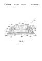
- a glob of encapsulant material 102(usually epoxy or silicone or a combination thereof) is generally applied to a COB assembly 100 to surround a semiconductor chip or flip chip 104 which is attached to a substrate 106 via a plurality of electrical connections 108 which extend between a plurality of semiconductor chip bond pads 110 and a corresponding plurality of substrate bond pads 112 .
- An under-fill encapsulant 114is dispensed between the semiconductor chip 104 and the substrate 106 .
- the glob top materials 202are often used to hermetically seal bare dice 204 (shown in shadow) on a printed circuit board 206 such as SIMM modules to form a COB assembly 200 .
- the organic resins generally used in the glob top encapsulationare usually selected for low moisture permeability and low thermal coefficient of expansion to avoid exposure of the encapsulated chip to moisture or mechanical stress respectively.
- the thermal and electrical propertiesare often not optimal for removing heat efficiently away from the semiconductor dice or for use in high temperature areas.
- Every semiconductor chip in a COB assemblygenerates some heat during operation. Some glob tops and package encapsulation materials serve to draw the heat away from most semiconductor chips. Indeed, one factor in choosing a package encapsulation material is its thermal dissipation properties. If the temperature of the semiconductor chip is not controlled or accommodated, system reliability problems may occur due to excess temperature rise during operation. The device/semiconductor junction temperature (the location of the heat source due to power dissipation) must be maintained below a limiting value such as 85° C. The primary reason to control this temperature is that switching voltage is a sensitive function of device temperature. In addition, various failure mechanisms are thermally activated and failure rates becomes excessive above the desired temperature limit.
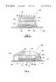
- FIG. 3illustrates a finned COB assembly 300 .
- the finned COB assembly 300comprises a semiconductor chip or flip chip 302 which is attached to a substrate 304 via a plurality of electrical connections 306 which extend between a plurality of semiconductor chip bond pads 308 and a corresponding plurality of substrate bond pads 310 .
- An under-fill encapsulant 312is dispensed between the semiconductor chip 302 and the substrate 304 .
- a cap 314 having a plurality of heat-dissipating fins 316is attached to an upper surface 318 of the semiconductor chip 302 with a layer of thermally conductive adhesive 320 .
- the addition of heat-dissipating fins, blocks or the likesubstantially increases the cost of production for COB assemblies.
- U.S. Pat. No. 5,434,105 issued Jul. 18, 1995 to Liourelates to the use of heat spreaders attached to a semiconductor by a glob top to strengthen the heat coupling from an integrated circuit die to the lead frame wherein heat can then pass through the leads of the lead frame to the circuit board.
- the heatis not dissipated away from the circuit. Rather, the heat is conducted into the circuit board, which can still cause heat related problems.
- U.S. Pat. No. 5,379,186 issued Jan. 3, 1995 to Gold et al.(“Gold”) relates to a heat producing semiconductor chip attached to a substrate which uses multiple encapsulants to dissipate heat.
- “Gold”teaches placing a layer of encapsulant material over the semiconductor chip with a layer of thermally conductive material applied over the encapsulant material layer.
- “Gold”specifically teaches that the encapsulant material layer used for covering the semiconductor is a relatively poor conductor of heat (i.e. an insulative material) which is assumedly chosen for its adherence and protective properties.
- the thermally conductive materialis applied over the encapsulant material to aid the removal of heat from the semiconductor through the insulating encapsulant material.
- this inventionis inherently inefficient since the heat must be drawn from an insulative material.
- the present inventionrelates to an apparatus and a method for providing a heat sink on a semiconductor chip.
- the apparatusis constructed with a two-step process for forming a dual material glob top.
- the processcomprises providing a semiconductor chip attached to and in electrical communication with a substrate by any known industry technique such as flip-chip attachment, TAB attachment, wirebonding and the like.
- a barrier glob top materialis applied to the edges of the semiconductor chip on the surface (“opposing surface”) opposite the surface (“attachment surface”) attached to the substrate to form a wall around a periphery of the opposing surface of the semiconductor chip and extends to contact and adhere to the substrate.
- the barrier glob topperforms the function of sealing and protecting the semiconductor chip.
- the barrier glob top materialis selected for low moisture permeability, low thermal coefficient of expansion, good adhesion and sealing properties.
- Preferred barrier glob top materialsinclude epoxy, polyamide, urethane silicone, acrylic or the like.
- the wall formed around the periphery of the opposing surfacepreferably covers and encapsulates the bond wires or TAB. If the semiconductor chip is a flip chip, an under-fill encapsulant may be disposed between the semiconductor chip and the substrate.
- the wall around the periphery of the opposing surface of the semiconductor chipforms a recess.
- a heat-dissipating glob top materialis disposed within the recess to contact the opposing surface for the semiconductor chip.
- the heat-dissipating glob top materialis chosen for its ability to transfer heat away from the semiconductor chip (i.e. high thermal conductivity material).
- the heat-dissipating glob top materialhas a higher thermal conductivity than the barrier glob top material.
- the heat-dissipating glob topmay also extend over the barrier glob top wall of the contact of the substrate.
- heat-dissipating glob top materialsinclude: standard, high purity barrier glob top materials containing arsenic, boron, gallium, germanium, phosphorus, silicon or other such suitable highly conductive materials.
- the apparatus of the present inventionhas all of the adherence and sealing benefits of a low thermal conductivity glob top material while at the same time enjoying the benefits of heat-dissipation provided by a high thermal conductivity glob top material.
- FIG. 1is a side cross-sectional view of a prior art glob top encapsulated semiconductor chip attached on a substrate;
- FIG. 2is an oblique plan view of a prior art substrate with a plurality of semiconductors attached to a substrate with a glob top encapsulation;
- FIG. 3is a side cross-sectional view of a prior art semiconductor assembly with heat-dissipating fins attached to a substrate;
- FIG. 4is a side cross-sectional view of a first encapsulated semiconductor assembly of the present invention.
- FIG. 5is an oblique plan view of the first encapsulated semiconductor assembly of FIG. 4;
- FIG. 6is a side cross-sectional view of a second encapsulated semiconductor assembly of the present invention.
- FIG. 7is a side cross-sectional view of a third encapsulated semiconductor assembly of the present invention.
- FIG. 8is a side cross-sectional view of a fourth encapsulated semiconductor assembly of the present invention.
- FIG. 9is a side cross-sectional view of a multiple encapsulated semiconductor dice assembly of the present invention.
- FIG. 4illustrates a first encapsulated semiconductor assembly 400 of the present invention.
- the first encapsulated semiconductor assembly 400comprises a flip chip or semiconductor chip 402 having a plurality of bond pads 404 on an active surface 406 of the semiconductor chip 402 .
- a facing surface 408 of each bond pad 404has a conductive pad 410 in electrical communication therewith.
- the conductive pads 410are in electrical communication with a plurality of respective bond pads 412 on an upper surface 414 of a substrate 416 .
- Each substrate bond pad 412is connected on a lower bond pad surface 418 to a trace lead 420 (shown by a dashed line).
- An under-fill encapsulant 422may be disposed between the semiconductor chip 402 and the substrate 416 .
- a barrier glob top 424is applied to surround a periphery of the semiconductor chip 402 which seals and protects the semiconductor chip 402 and forms a recess or cavity 426 .
- a heat-dissipating glob top 428is disposed within the recess 426 as shown in FIG. 4 .
- FIG. 6illustrates a second encapsulated semiconductor assembly 600 of the present invention.
- the encapsulated semiconductor assembly 600comprises a semiconductor chip 602 attached by a back side 604 of the semiconductor chip 602 to a facing surface 606 of a substrate 608 .
- the semiconductor chip 602has a plurality of bond pads 610 on an active surface 612 of the semiconductor chip 602 .
- a facing surface 614 of each bond pad 610has a bond wire 616 in electrical communication therewith.
- Each bond wire 616is in electrical communication with a respective bond pad 620 on the substrate facing surface 606 .
- Each substrate bond pad 620is connected on a lower bond pad surface 622 to a trace lead 624 (shown by a dashed line).
- a barrier glob top 626is applied to surround a periphery of the semiconductor chip 602 , forming a recess or cavity 628 .
- a heat-dissipating glob top 630is disposed within the recess 628 .
- FIG. 7illustrates a third encapsulated semiconductor assembly 700 of the present invention.
- the third encapsulated semiconductor assembly 700is similar to the second encapsulated semiconductor assembly 600 , therefore components common to FIGS. 6 and 7 retain the same numeric designation.
- the difference between the third encapsulated semiconductor assembly 700 and the second encapsulated semiconductor assembly 600is that the third encapsulated semiconductor assembly 700 has a plurality of TAB attachments 702 forming an electrical communication between the facing surface 614 of the semiconductor chip bond pad 610 and the substrate bond pads 620 rather than the bond wires 616 of the second encapsulated semiconductor assembly 600 .
- FIG. 8illustrates a fourth encapsulated semiconductor assembly 800 of the present invention.
- the fourth encapsulated semiconductor assembly 800is similar to the second encapsulated semiconductor assembly 600 , therefore components common to FIGS. 6 and 8 retain the same numeric designation.
- the difference between the fourth encapsulated semiconductor assembly 800 and the second encapsulated semiconductor assembly 600is that the fourth encapsulated semiconductor assembly 800 has a heat-dissipating glob top 802 which is disposed within the recess 628 and extends over the barrier glob top 626 to contact and adhere to the substrate 608 .
- FIG. 9illustrates a multiple encapsulated semiconductor dice assembly 900 of the present invention.
- the multiple encapsulated semiconductor dice assembly 900is similar to the fourth encapsulated semiconductor assembly 800 , therefore components common to FIGS. 8 and 9 retain the same numeric designation.
- the difference between the multiple encapsulated semiconductor dice assembly 900 and the fourth encapsulated semiconductor assembly 800is that the multiple encapsulated semiconductor dice assembly 900 has multiple semiconductor dice 902 and 904 with a heat-dissipating glob top 802 which extends over the semiconductor dice 902 and 904 to contact and adhere to the substrate 608 .
Landscapes
- Engineering & Computer Science (AREA)
- Microelectronics & Electronic Packaging (AREA)
- Power Engineering (AREA)
- Computer Hardware Design (AREA)
- Physics & Mathematics (AREA)
- Condensed Matter Physics & Semiconductors (AREA)
- General Physics & Mathematics (AREA)
- Manufacturing & Machinery (AREA)
- Cooling Or The Like Of Semiconductors Or Solid State Devices (AREA)
Abstract
Description
Claims (69)
Priority Applications (6)
| Application Number | Priority Date | Filing Date | Title |
|---|---|---|---|
| US09/189,102US6252308B1 (en) | 1996-05-24 | 1998-11-09 | Packaged die PCB with heat sink encapsulant |
| US09/835,541US6534858B2 (en) | 1996-05-24 | 2001-04-16 | Assembly and methods for packaged die on pcb with heat sink encapsulant |
| US10/232,782US6617684B2 (en) | 1996-05-24 | 2002-08-28 | Packaged die on PCB with heat sink encapsulant |
| US10/639,349US6853069B2 (en) | 1996-05-24 | 2003-08-12 | Packaged die on PCB with heat sink encapsulant and methods |
| US11/053,082US20050189646A1 (en) | 1996-05-24 | 2005-02-07 | Packaged die on PCB with heat sink encapsulant and methods |
| US11/603,581US20070069372A1 (en) | 1996-05-24 | 2006-11-22 | Packaged die on PCB with heat sink encapsulant and methods |
Applications Claiming Priority (2)
| Application Number | Priority Date | Filing Date | Title |
|---|---|---|---|
| US08/653,030US5866953A (en) | 1996-05-24 | 1996-05-24 | Packaged die on PCB with heat sink encapsulant |
| US09/189,102US6252308B1 (en) | 1996-05-24 | 1998-11-09 | Packaged die PCB with heat sink encapsulant |
Related Parent Applications (1)
| Application Number | Title | Priority Date | Filing Date |
|---|---|---|---|
| US08/653,030ContinuationUS5866953A (en) | 1996-05-24 | 1996-05-24 | Packaged die on PCB with heat sink encapsulant |
Related Child Applications (1)
| Application Number | Title | Priority Date | Filing Date |
|---|---|---|---|
| US09/835,541ContinuationUS6534858B2 (en) | 1996-05-24 | 2001-04-16 | Assembly and methods for packaged die on pcb with heat sink encapsulant |
Publications (1)
| Publication Number | Publication Date |
|---|---|
| US6252308B1true US6252308B1 (en) | 2001-06-26 |
Family
ID=24619213
Family Applications (7)
| Application Number | Title | Priority Date | Filing Date |
|---|---|---|---|
| US08/653,030Expired - LifetimeUS5866953A (en) | 1996-05-24 | 1996-05-24 | Packaged die on PCB with heat sink encapsulant |
| US09/189,102Expired - LifetimeUS6252308B1 (en) | 1996-05-24 | 1998-11-09 | Packaged die PCB with heat sink encapsulant |
| US09/835,541Expired - LifetimeUS6534858B2 (en) | 1996-05-24 | 2001-04-16 | Assembly and methods for packaged die on pcb with heat sink encapsulant |
| US10/232,782Expired - LifetimeUS6617684B2 (en) | 1996-05-24 | 2002-08-28 | Packaged die on PCB with heat sink encapsulant |
| US10/639,349Expired - Fee RelatedUS6853069B2 (en) | 1996-05-24 | 2003-08-12 | Packaged die on PCB with heat sink encapsulant and methods |
| US11/053,082AbandonedUS20050189646A1 (en) | 1996-05-24 | 2005-02-07 | Packaged die on PCB with heat sink encapsulant and methods |
| US11/603,581AbandonedUS20070069372A1 (en) | 1996-05-24 | 2006-11-22 | Packaged die on PCB with heat sink encapsulant and methods |
Family Applications Before (1)
| Application Number | Title | Priority Date | Filing Date |
|---|---|---|---|
| US08/653,030Expired - LifetimeUS5866953A (en) | 1996-05-24 | 1996-05-24 | Packaged die on PCB with heat sink encapsulant |
Family Applications After (5)
| Application Number | Title | Priority Date | Filing Date |
|---|---|---|---|
| US09/835,541Expired - LifetimeUS6534858B2 (en) | 1996-05-24 | 2001-04-16 | Assembly and methods for packaged die on pcb with heat sink encapsulant |
| US10/232,782Expired - LifetimeUS6617684B2 (en) | 1996-05-24 | 2002-08-28 | Packaged die on PCB with heat sink encapsulant |
| US10/639,349Expired - Fee RelatedUS6853069B2 (en) | 1996-05-24 | 2003-08-12 | Packaged die on PCB with heat sink encapsulant and methods |
| US11/053,082AbandonedUS20050189646A1 (en) | 1996-05-24 | 2005-02-07 | Packaged die on PCB with heat sink encapsulant and methods |
| US11/603,581AbandonedUS20070069372A1 (en) | 1996-05-24 | 2006-11-22 | Packaged die on PCB with heat sink encapsulant and methods |
Country Status (1)
| Country | Link |
|---|---|
| US (7) | US5866953A (en) |
Cited By (34)
| Publication number | Priority date | Publication date | Assignee | Title |
|---|---|---|---|---|
| US6365441B1 (en) | 1999-12-29 | 2002-04-02 | Intel Corporation | Partial underfill for flip-chip electronic packages |
| US6444501B1 (en)* | 2001-06-12 | 2002-09-03 | Micron Technology, Inc. | Two stage transfer molding method to encapsulate MMC module |
| US6534858B2 (en)* | 1996-05-24 | 2003-03-18 | Micron Technology, Inc. | Assembly and methods for packaged die on pcb with heat sink encapsulant |
| US20030159278A1 (en)* | 2002-02-26 | 2003-08-28 | Peddle Charles I. | Methods and apparatus for fabricating Chip-on-Board modules |
| US20030189262A1 (en)* | 2002-04-04 | 2003-10-09 | Tongbi Jiang | Method and apparatus for attaching microelectronic substrates and support members |
| EP1365450A1 (en)* | 2002-05-24 | 2003-11-26 | Ultratera Corporation | An improved wire-bonded chip on board package |
| US6660943B1 (en)* | 1999-07-08 | 2003-12-09 | Sunstar Giken Kabushiki Kaisha | Underfilling material for semiconductor package |
| US6737299B1 (en) | 1999-06-08 | 2004-05-18 | Micron Technology, Inc. | Thermally conductive adhesive tape for semiconductor devices and method for using the same |
| US20040173899A1 (en)* | 2003-03-04 | 2004-09-09 | Peng Neo Chee | Microelectronic component assemblies employing lead frames having reduced-thickness inner lengths |
| US20040233035A1 (en)* | 1996-04-18 | 2004-11-25 | Tessera, Inc. | Methods for manufacturing resistors using a sacrificial layer |
| US20040266068A1 (en)* | 2003-06-30 | 2004-12-30 | Matayabas J. Christopher | Wire-bonded package with electrically insulating wire encapsulant and thermally conductive overmold |
| US20050093174A1 (en)* | 2003-10-31 | 2005-05-05 | Seng Eric T.S. | Reduced footprint packaged microelectronic components and methods for manufacturing such microelectronic components |
| US6921860B2 (en) | 2003-03-18 | 2005-07-26 | Micron Technology, Inc. | Microelectronic component assemblies having exposed contacts |
| US20060017177A1 (en)* | 2004-07-23 | 2006-01-26 | Seng Eric T S | Microelectronic component assemblies with recessed wire bonds and methods of making same |
| US20060046346A1 (en)* | 2004-09-01 | 2006-03-02 | Benson Peter A | Methods for packaging microfeature devices and microfeature devices formed by such methods |
| US20060044773A1 (en)* | 2004-08-25 | 2006-03-02 | Micron Technology, Inc. | Methods and apparatuses for transferring heat from stacked microfeature devices |
| US20060177970A1 (en)* | 2005-02-08 | 2006-08-10 | Micron Technology, Inc. | Methods of Adhering Microfeature Workpieces, Including A Chip, To A Support Member |
| US7122905B2 (en) | 2002-02-12 | 2006-10-17 | Micron Technology, Inc. | Microelectronic devices and methods for mounting microelectronic packages to circuit boards |
| US20070031998A1 (en)* | 2000-08-16 | 2007-02-08 | Micron Technology, Inc. | Method and apparatus for removing encapsulating material from a packaged microelectronic device |
| US20070045875A1 (en)* | 2005-08-30 | 2007-03-01 | Micron Technology, Inc. | Methods for wafer-level packaging of microfeature devices and microfeature devices formed using such methods |
| US20070148820A1 (en)* | 2005-12-22 | 2007-06-28 | Micron Technology, Inc. | Microelectronic devices and methods for manufacturing microelectronic devices |
| US20070155048A1 (en)* | 2005-12-29 | 2007-07-05 | Micron Technology, Inc. | Methods for packaging microelectronic devices and microelectronic devices formed using such methods |
| US20070228577A1 (en)* | 2006-03-29 | 2007-10-04 | Micron Technology, Inc. | Packaged microelectronic devices recessed in support member cavities, and associated methods |
| US20070262436A1 (en)* | 2006-05-12 | 2007-11-15 | Micron Technology, Inc. | Microelectronic devices and methods for manufacturing microelectronic devices |
| US20080224329A1 (en)* | 2007-03-13 | 2008-09-18 | Micron Technology, Inc. | Packaged microelectronic devices and methods for manufacturing packaged microelectronic devices |
| US20080224291A1 (en)* | 2007-03-13 | 2008-09-18 | Micron Technology, Inc. | Packaged semiconductor components having substantially rigid support members and methods of packaging semiconductor components |
| US20090152692A1 (en)* | 2007-12-12 | 2009-06-18 | Seng Guan Chow | Integrated circuit package system with offset stacking |
| US20090152706A1 (en)* | 2007-12-12 | 2009-06-18 | Heap Hoe Kuan | Integrated circuit package system with interconnect lock |
| US20090155960A1 (en)* | 2007-12-12 | 2009-06-18 | Seng Guan Chow | Integrated circuit package system with offset stacking and anti-flash structure |
| US20090152700A1 (en)* | 2007-12-12 | 2009-06-18 | Heap Hoe Kuan | Mountable integrated circuit package system with mountable integrated circuit die |
| US20090243069A1 (en)* | 2008-03-26 | 2009-10-01 | Zigmund Ramirez Camacho | Integrated circuit package system with redistribution |
| US20100025833A1 (en)* | 2008-07-30 | 2010-02-04 | Reza Argenty Pagaila | Rdl patterning with package on package system |
| US7745944B2 (en) | 2005-08-31 | 2010-06-29 | Micron Technology, Inc. | Microelectronic devices having intermediate contacts for connection to interposer substrates, and associated methods of packaging microelectronic devices with intermediate contacts |
| US9933577B2 (en) | 2016-03-11 | 2018-04-03 | Globalfoundries Inc. | Photonics chip |
Families Citing this family (151)
| Publication number | Priority date | Publication date | Assignee | Title |
|---|---|---|---|---|
| US6097089A (en)* | 1998-01-28 | 2000-08-01 | Mitsubishi Gas Chemical Company, Inc. | Semiconductor plastic package, metal plate for said package, and method of producing copper-clad board for said package |
| JP3834335B2 (en)* | 1996-08-08 | 2006-10-18 | セイコーエプソン株式会社 | Resin coating method for semiconductor element and liquid crystal display device |
| US6962829B2 (en)* | 1996-10-31 | 2005-11-08 | Amkor Technology, Inc. | Method of making near chip size integrated circuit package |
| KR100246333B1 (en)* | 1997-03-14 | 2000-03-15 | 김영환 | Ball grid array package and method for manufacturing thereof |
| JPH10335383A (en)* | 1997-05-28 | 1998-12-18 | Matsushita Electric Ind Co Ltd | Method for manufacturing semiconductor device |
| US5962810A (en)* | 1997-09-09 | 1999-10-05 | Amkor Technology, Inc. | Integrated circuit package employing a transparent encapsulant |
| US6204564B1 (en)* | 1997-11-21 | 2001-03-20 | Rohm Co., Ltd. | Semiconductor device and method for making the same |
| US7233056B1 (en)* | 1998-02-23 | 2007-06-19 | Micron Technology, Inc. | Chip scale package with heat spreader |
| US6297548B1 (en) | 1998-06-30 | 2001-10-02 | Micron Technology, Inc. | Stackable ceramic FBGA for high thermal applications |
| US6297960B1 (en) | 1998-06-30 | 2001-10-02 | Micron Technology, Inc. | Heat sink with alignment and retaining features |
| US6092281A (en) | 1998-08-28 | 2000-07-25 | Amkor Technology, Inc. | Electromagnetic interference shield driver and method |
| US6117797A (en) | 1998-09-03 | 2000-09-12 | Micron Technology, Inc. | Attachment method for heat sinks and devices involving removal of misplaced encapsulant |
| US6184465B1 (en)* | 1998-11-12 | 2001-02-06 | Micron Technology, Inc. | Semiconductor package |
| US6507101B1 (en)* | 1999-03-26 | 2003-01-14 | Hewlett-Packard Company | Lossy RF shield for integrated circuits |
| US6211574B1 (en)* | 1999-04-16 | 2001-04-03 | Advanced Semiconductor Engineering Inc. | Semiconductor package with wire protection and method therefor |
| JP2000306948A (en)* | 1999-04-21 | 2000-11-02 | Rohm Co Ltd | Semiconductor device and manufacture thereof |
| SE514076C2 (en) | 1999-04-23 | 2000-12-18 | Ericsson Telefon Ab L M | Method and apparatus related to microwave lens |
| US6048656A (en)* | 1999-05-11 | 2000-04-11 | Micron Technology, Inc. | Void-free underfill of surface mounted chips |
| US6274927B1 (en) | 1999-06-03 | 2001-08-14 | Amkor Technology, Inc. | Plastic package for an optical integrated circuit device and method of making |
| US6122171A (en)* | 1999-07-30 | 2000-09-19 | Micron Technology, Inc. | Heat sink chip package and method of making |
| US6709968B1 (en) | 2000-08-16 | 2004-03-23 | Micron Technology, Inc. | Microelectronic device with package with conductive elements and associated method of manufacture |
| US6670719B2 (en) | 1999-08-25 | 2003-12-30 | Micron Technology, Inc. | Microelectronic device package filled with liquid or pressurized gas and associated method of manufacture |
| US6448635B1 (en) | 1999-08-30 | 2002-09-10 | Amkor Technology, Inc. | Surface acoustical wave flip chip |
| KR20010054743A (en)* | 1999-12-08 | 2001-07-02 | 윤종용 | Semiconductor package comprising double underfill area |
| US6468891B2 (en)* | 2000-02-24 | 2002-10-22 | Micron Technology, Inc. | Stereolithographically fabricated conductive elements, semiconductor device components and assemblies including such conductive elements, and methods |
| US6949822B2 (en)* | 2000-03-17 | 2005-09-27 | International Rectifier Corporation | Semiconductor multichip module package with improved thermal performance; reduced size and improved moisture resistance |
| CN1211723C (en)* | 2000-04-04 | 2005-07-20 | 胜开科技股份有限公司 | Computer card making method |
| US6558600B1 (en) | 2000-05-04 | 2003-05-06 | Micron Technology, Inc. | Method for packaging microelectronic substrates |
| US6611053B2 (en)* | 2000-06-08 | 2003-08-26 | Micron Technology, Inc. | Protective structure for bond wires |
| US6589820B1 (en) | 2000-06-16 | 2003-07-08 | Micron Technology, Inc. | Method and apparatus for packaging a microelectronic die |
| US6576494B1 (en)* | 2000-06-28 | 2003-06-10 | Micron Technology, Inc. | Recessed encapsulated microelectronic devices and methods for formation |
| US6483044B1 (en)* | 2000-08-23 | 2002-11-19 | Micron Technology, Inc. | Interconnecting substrates for electrical coupling of microelectronic components |
| US6979595B1 (en) | 2000-08-24 | 2005-12-27 | Micron Technology, Inc. | Packaged microelectronic devices with pressure release elements and methods for manufacturing and using such packaged microelectronic devices |
| US6838760B1 (en)* | 2000-08-28 | 2005-01-04 | Micron Technology, Inc. | Packaged microelectronic devices with interconnecting units |
| US6576495B1 (en) | 2000-08-30 | 2003-06-10 | Micron Technology, Inc. | Microelectronic assembly with pre-disposed fill material and associated method of manufacture |
| US6787388B1 (en)* | 2000-09-07 | 2004-09-07 | Stmicroelectronics, Inc. | Surface mount package with integral electro-static charge dissipating ring using lead frame as ESD device |
| TW469609B (en)* | 2000-10-11 | 2001-12-21 | Ultratera Corp | Chipless package semiconductor device and its manufacturing method |
| US6564447B1 (en)* | 2000-11-15 | 2003-05-20 | National Semiconductor Corporation | Non lead frame clamping for matrix leadless leadframe package molding |
| US6545869B2 (en)* | 2001-01-17 | 2003-04-08 | International Business Machines Corporation | Adjusting fillet geometry to couple a heat spreader to a chip carrier |
| JP4626919B2 (en)* | 2001-03-27 | 2011-02-09 | ルネサスエレクトロニクス株式会社 | Semiconductor device |
| US7115986B2 (en)* | 2001-05-02 | 2006-10-03 | Micron Technology, Inc. | Flexible ball grid array chip scale packages |
| DE10137666A1 (en)* | 2001-08-01 | 2003-02-27 | Infineon Technologies Ag | Protection device for assemblies and process for their manufacture |
| SG122743A1 (en)* | 2001-08-21 | 2006-06-29 | Micron Technology Inc | Microelectronic devices and methods of manufacture |
| US6861720B1 (en) | 2001-08-29 | 2005-03-01 | Amkor Technology, Inc. | Placement template and method for placing optical dies |
| SG111919A1 (en)* | 2001-08-29 | 2005-06-29 | Micron Technology Inc | Packaged microelectronic devices and methods of forming same |
| SG104293A1 (en) | 2002-01-09 | 2004-06-21 | Micron Technology Inc | Elimination of rdl using tape base flip chip on flex for die stacking |
| US6784534B1 (en) | 2002-02-06 | 2004-08-31 | Amkor Technology, Inc. | Thin integrated circuit package having an optically transparent window |
| SG115459A1 (en)* | 2002-03-04 | 2005-10-28 | Micron Technology Inc | Flip chip packaging using recessed interposer terminals |
| SG121707A1 (en)* | 2002-03-04 | 2006-05-26 | Micron Technology Inc | Method and apparatus for flip-chip packaging providing testing capability |
| US6975035B2 (en)* | 2002-03-04 | 2005-12-13 | Micron Technology, Inc. | Method and apparatus for dielectric filling of flip chip on interposer assembly |
| SG111935A1 (en) | 2002-03-04 | 2005-06-29 | Micron Technology Inc | Interposer configured to reduce the profiles of semiconductor device assemblies and packages including the same and methods |
| SG115455A1 (en)* | 2002-03-04 | 2005-10-28 | Micron Technology Inc | Methods for assembly and packaging of flip chip configured dice with interposer |
| SG115456A1 (en) | 2002-03-04 | 2005-10-28 | Micron Technology Inc | Semiconductor die packages with recessed interconnecting structures and methods for assembling the same |
| US6745462B2 (en) | 2002-03-07 | 2004-06-08 | Kulicke & Soffa Industries, Inc. | Method and apparatus for reducing deformation of encapsulant in semiconductor device encapsulation by stencil printing |
| US6844618B2 (en)* | 2002-04-04 | 2005-01-18 | Micron Technology, Inc. | Microelectronic package with reduced underfill and methods for forming such packages |
| US6534859B1 (en)* | 2002-04-05 | 2003-03-18 | St. Assembly Test Services Ltd. | Semiconductor package having heat sink attached to pre-molded cavities and method for creating the package |
| US6673649B1 (en)* | 2002-07-05 | 2004-01-06 | Micron Technology, Inc. | Microelectronic device packages and methods for controlling the disposition of non-conductive materials in such packages |
| US6979594B1 (en) | 2002-07-19 | 2005-12-27 | Asat Ltd. | Process for manufacturing ball grid array package |
| US6987032B1 (en) | 2002-07-19 | 2006-01-17 | Asat Ltd. | Ball grid array package and process for manufacturing same |
| US6800948B1 (en) | 2002-07-19 | 2004-10-05 | Asat Ltd. | Ball grid array package |
| SG120879A1 (en)* | 2002-08-08 | 2006-04-26 | Micron Technology Inc | Packaged microelectronic components |
| SG127684A1 (en)* | 2002-08-19 | 2006-12-29 | Micron Technology Inc | Packaged microelectronic component assemblies |
| US20040036170A1 (en)* | 2002-08-20 | 2004-02-26 | Lee Teck Kheng | Double bumping of flexible substrate for first and second level interconnects |
| SG114585A1 (en)* | 2002-11-22 | 2005-09-28 | Micron Technology Inc | Packaged microelectronic component assemblies |
| JP3793143B2 (en)* | 2002-11-28 | 2006-07-05 | 株式会社シマノ | Bicycle electronic control device |
| US7199459B2 (en)* | 2003-01-22 | 2007-04-03 | Siliconware Precision Industries Co., Ltd. | Semiconductor package without bonding wires and fabrication method thereof |
| JP4390541B2 (en)* | 2003-02-03 | 2009-12-24 | Necエレクトロニクス株式会社 | Semiconductor device and manufacturing method thereof |
| US6768209B1 (en) | 2003-02-03 | 2004-07-27 | Micron Technology, Inc. | Underfill compounds including electrically charged filler elements, microelectronic devices having underfill compounds including electrically charged filler elements, and methods of underfilling microelectronic devices |
| US6879050B2 (en)* | 2003-02-11 | 2005-04-12 | Micron Technology, Inc. | Packaged microelectronic devices and methods for packaging microelectronic devices |
| JP3947525B2 (en)* | 2003-04-16 | 2007-07-25 | 沖電気工業株式会社 | Semiconductor device heat dissipation structure |
| US7180169B2 (en)* | 2003-08-28 | 2007-02-20 | Matsushita Electric Industrial Co., Ltd. | Circuit component built-in module and method for manufacturing the same |
| US7368810B2 (en) | 2003-08-29 | 2008-05-06 | Micron Technology, Inc. | Invertible microfeature device packages |
| US7372151B1 (en) | 2003-09-12 | 2008-05-13 | Asat Ltd. | Ball grid array package and process for manufacturing same |
| US6888719B1 (en)* | 2003-10-16 | 2005-05-03 | Micron Technology, Inc. | Methods and apparatuses for transferring heat from microelectronic device modules |
| TWI228304B (en)* | 2003-10-29 | 2005-02-21 | Advanced Semiconductor Eng | Method for manufacturing ball grid package |
| TWI238499B (en)* | 2003-11-03 | 2005-08-21 | Siliconware Precision Industries Co Ltd | Semiconductor package |
| US20050110168A1 (en)* | 2003-11-20 | 2005-05-26 | Texas Instruments Incorporated | Low coefficient of thermal expansion (CTE) semiconductor packaging materials |
| US7154185B2 (en)* | 2003-11-20 | 2006-12-26 | Taiwan Semiconductor Manufacturing Co., Ltd. | Encapsulation method for SBGA |
| US7081669B2 (en)* | 2003-12-04 | 2006-07-25 | Intel Corporation | Device and system for heat spreader with controlled thermal expansion |
| US7153725B2 (en)* | 2004-01-27 | 2006-12-26 | St Assembly Test Services Ltd. | Strip-fabricated flip chip in package and flip chip in system heat spreader assemblies and fabrication methods therefor |
| JP2005311321A (en)* | 2004-03-22 | 2005-11-04 | Sharp Corp | SEMICONDUCTOR DEVICE, ITS MANUFACTURING METHOD, AND LIQUID CRYSTAL MODULE AND SEMICONDUCTOR MODULE HAVING THE SEMICONDUCTOR DEVICE |
| US20050247039A1 (en)* | 2004-05-04 | 2005-11-10 | Textron Inc. | Disposable magnetic bedknife |
| DE102004027074B4 (en)* | 2004-06-02 | 2009-06-04 | Infineon Technologies Ag | Method for producing a BGA (Ball Grid Array) component with a thin metallic cooling foil |
| US7411289B1 (en) | 2004-06-14 | 2008-08-12 | Asat Ltd. | Integrated circuit package with partially exposed contact pads and process for fabricating the same |
| US7091581B1 (en) | 2004-06-14 | 2006-08-15 | Asat Limited | Integrated circuit package and process for fabricating the same |
| US20060103008A1 (en)* | 2004-11-15 | 2006-05-18 | Stats Chippac Ltd. | Hyper thermally enhanced semiconductor package system |
| US8164182B2 (en)* | 2004-11-15 | 2012-04-24 | Stats Chippac Ltd. | Hyper thermally enhanced semiconductor package system comprising heat slugs on opposite surfaces of a semiconductor chip |
| US20060162850A1 (en)* | 2005-01-24 | 2006-07-27 | Micron Technology, Inc. | Methods and apparatus for releasably attaching microfeature workpieces to support members |
| US7968371B2 (en)* | 2005-02-01 | 2011-06-28 | Stats Chippac Ltd. | Semiconductor package system with cavity substrate |
| TWI254422B (en)* | 2005-02-17 | 2006-05-01 | Advanced Semiconductor Eng | Chip package and producing method thereof |
| US8610262B1 (en) | 2005-02-18 | 2013-12-17 | Utac Hong Kong Limited | Ball grid array package with improved thermal characteristics |
| DE102005014674B4 (en)* | 2005-03-29 | 2010-02-11 | Infineon Technologies Ag | Semiconductor module with semiconductor chips in a plastic housing in separate areas and method for producing the same |
| US20060261498A1 (en)* | 2005-05-17 | 2006-11-23 | Micron Technology, Inc. | Methods and apparatuses for encapsulating microelectronic devices |
| DE102005023949B4 (en)* | 2005-05-20 | 2019-07-18 | Infineon Technologies Ag | A method of manufacturing a composite panel with semiconductor chips and a plastic package and a method of manufacturing semiconductor components by means of a benefit |
| US7573125B2 (en)* | 2005-06-14 | 2009-08-11 | Micron Technology, Inc. | Methods for reducing stress in microelectronic devices and microelectronic devices formed using such methods |
| US7169248B1 (en)* | 2005-07-19 | 2007-01-30 | Micron Technology, Inc. | Methods for releasably attaching support members to microfeature workpieces and microfeature assemblies formed using such methods |
| US20090127690A1 (en)* | 2005-07-28 | 2009-05-21 | Nxp B.V. | Package and Manufacturing Method for a Microelectronic Component |
| CN100479136C (en)* | 2006-01-06 | 2009-04-15 | 日月光半导体制造股份有限公司 | Chip packaging structure and manufacturing method thereof |
| CN100470771C (en)* | 2006-01-09 | 2009-03-18 | 日月光半导体制造股份有限公司 | Chip packaging structure and manufacturing method thereof |
| SG135074A1 (en) | 2006-02-28 | 2007-09-28 | Micron Technology Inc | Microelectronic devices, stacked microelectronic devices, and methods for manufacturing such devices |
| DE102006007303A1 (en)* | 2006-02-16 | 2007-08-30 | Infineon Technologies Ag | Printed circuit board, has grouting cover element, in which multiple chips connected electrically with printed circuit board, are embedded |
| US7749349B2 (en)* | 2006-03-14 | 2010-07-06 | Micron Technology, Inc. | Methods and systems for releasably attaching support members to microfeature workpieces |
| US7985623B2 (en)* | 2006-04-14 | 2011-07-26 | Stats Chippac Ltd. | Integrated circuit package system with contoured encapsulation |
| JP5481769B2 (en)* | 2006-11-22 | 2014-04-23 | 日亜化学工業株式会社 | Semiconductor device and manufacturing method thereof |
| US7833456B2 (en)* | 2007-02-23 | 2010-11-16 | Micron Technology, Inc. | Systems and methods for compressing an encapsulant adjacent a semiconductor workpiece |
| JP5075463B2 (en)* | 2007-04-19 | 2012-11-21 | ルネサスエレクトロニクス株式会社 | Semiconductor device |
| DE102007020656B4 (en) | 2007-04-30 | 2009-05-07 | Infineon Technologies Ag | Semiconductor chip workpiece, semiconductor device, and method of manufacturing a semiconductor chip workpiece |
| US7687895B2 (en)* | 2007-04-30 | 2010-03-30 | Infineon Technologies Ag | Workpiece with semiconductor chips and molding, semiconductor device and method for producing a workpiece with semiconductors chips |
| US7714426B1 (en)* | 2007-07-07 | 2010-05-11 | Keith Gann | Ball grid array package format layers and structure |
| US20090079097A1 (en)* | 2007-09-25 | 2009-03-26 | Silverbrook Research Pty Ltd | Electronic component with wire bonds in low modulus fill encapsulant |
| US20090127700A1 (en)* | 2007-11-20 | 2009-05-21 | Matthew Romig | Thermal conductor lids for area array packaged multi-chip modules and methods to dissipate heat from multi-chip modules |
| US8659154B2 (en) | 2008-03-14 | 2014-02-25 | Infineon Technologies Ag | Semiconductor device including adhesive covered element |
| SG142321A1 (en) | 2008-04-24 | 2009-11-26 | Micron Technology Inc | Pre-encapsulated cavity interposer |
| JP4560113B2 (en)* | 2008-09-30 | 2010-10-13 | 株式会社東芝 | Printed circuit board and electronic device provided with printed circuit board |
| US8472199B2 (en)* | 2008-11-13 | 2013-06-25 | Mosaid Technologies Incorporated | System including a plurality of encapsulated semiconductor chips |
| EP2423955B8 (en)* | 2009-04-24 | 2019-10-09 | Panasonic Intellectual Property Management Co., Ltd. | Method for mounting semiconductor package component, and structure having semiconductor package component mounted therein |
| JP5062283B2 (en) | 2009-04-30 | 2012-10-31 | 日亜化学工業株式会社 | Semiconductor device and manufacturing method thereof |
| JP4676012B2 (en)* | 2009-06-03 | 2011-04-27 | 株式会社東芝 | Electronics |
| US9230874B1 (en)* | 2009-07-13 | 2016-01-05 | Altera Corporation | Integrated circuit package with a heat conductor |
| US8535989B2 (en) | 2010-04-02 | 2013-09-17 | Intel Corporation | Embedded semiconductive chips in reconstituted wafers, and systems containing same |
| JP2012009713A (en)* | 2010-06-25 | 2012-01-12 | Shinko Electric Ind Co Ltd | Semiconductor package and method of manufacturing the same |
| JP2012015225A (en)* | 2010-06-30 | 2012-01-19 | Hitachi Ltd | Semiconductor device |
| EP2466655A1 (en)* | 2010-12-14 | 2012-06-20 | Liang Meng Plastic Share Co. Ltd. | LED package structure and manufacturing method for the same |
| US8937382B2 (en) | 2011-06-27 | 2015-01-20 | Intel Corporation | Secondary device integration into coreless microelectronic device packages |
| US8848380B2 (en)* | 2011-06-30 | 2014-09-30 | Intel Corporation | Bumpless build-up layer package warpage reduction |
| KR20130026062A (en)* | 2011-09-05 | 2013-03-13 | 삼성전자주식회사 | Printed Circuit Board Assembly and Manufacturing Method Thereof |
| US9093416B2 (en)* | 2011-11-28 | 2015-07-28 | Infineon Technologies Ag | Chip-package and a method for forming a chip-package |
| US20130242538A1 (en)* | 2012-03-13 | 2013-09-19 | Shenzhen China Star Optoelectronics Technology Co Ltd. | Led light bar and backlight module |
| WO2013172814A1 (en) | 2012-05-14 | 2013-11-21 | Intel Corporation | Microelectronic package utilizing multiple bumpless build-up structures and through-silicon vias |
| US9685390B2 (en) | 2012-06-08 | 2017-06-20 | Intel Corporation | Microelectronic package having non-coplanar, encapsulated microelectronic devices and a bumpless build-up layer |
| JP2014013836A (en)* | 2012-07-04 | 2014-01-23 | Ps4 Luxco S A R L | Semiconductor device |
| KR101506130B1 (en)* | 2012-09-06 | 2015-03-26 | 시그네틱스 주식회사 | PBGA package having a reinforcement resin |
| JP5942308B2 (en)* | 2012-09-06 | 2016-06-29 | パナソニックIpマネジメント株式会社 | Mounting structure and method for supplying reinforcing resin material |
| US9847317B2 (en)* | 2014-07-08 | 2017-12-19 | Taiwan Semiconductor Manufacturing Company, Ltd. | Methods of packaging semiconductor devices and packaged semiconductor devices |
| US9165794B1 (en)* | 2014-07-31 | 2015-10-20 | Himax Display, Inc. | Partial glob-top encapsulation technique |
| TWI594341B (en)* | 2015-01-19 | 2017-08-01 | 神盾股份有限公司 | Fingerprint sensor package and method for fabricating the same |
| DE102015120109B4 (en)* | 2015-11-19 | 2018-03-01 | Danfoss Silicon Power Gmbh | Power semiconductor module with a power semiconductor covering Glob-top potting compound |
| JP2018098487A (en)* | 2016-12-14 | 2018-06-21 | 株式会社村田製作所 | Semiconductor module |
| US10279610B2 (en) | 2016-12-20 | 2019-05-07 | Xerox Corporation | Cooling insert |
| EP3340293A1 (en)* | 2016-12-20 | 2018-06-27 | Siemens Aktiengesellschaft | Semiconductor module with support structure on the bottom |
| KR102639555B1 (en)* | 2017-01-13 | 2024-02-23 | 삼성전자주식회사 | EMI shielding structure having heat dissipation unit and manufacturing method the same |
| US10217649B2 (en)* | 2017-06-09 | 2019-02-26 | Advanced Semiconductor Engineering, Inc. | Semiconductor device package having an underfill barrier |
| US10211072B2 (en)* | 2017-06-23 | 2019-02-19 | Applied Materials, Inc. | Method of reconstituted substrate formation for advanced packaging applications |
| US11152274B2 (en)* | 2017-09-11 | 2021-10-19 | Advanced Semiconductor Engineering, Inc. | Multi-moldings fan-out package and process |
| US10957672B2 (en)* | 2017-11-13 | 2021-03-23 | Taiwan Semiconductor Manufacturing Company, Ltd. | Package structure and method of manufacturing the same |
| US10879195B2 (en)* | 2018-02-15 | 2020-12-29 | Micron Technology, Inc. | Method for substrate moisture NCF voiding elimination |
| CN117936471A (en)* | 2018-07-20 | 2024-04-26 | 罗姆股份有限公司 | Semiconductor device and SiC semiconductor device |
| KR102633142B1 (en) | 2019-08-26 | 2024-02-02 | 삼성전자주식회사 | Semiconductor package |
| KR20220003342A (en)* | 2020-07-01 | 2022-01-10 | 삼성전기주식회사 | Electronic component pagkage and manufacturing method thereof |
| KR20220018645A (en)* | 2020-08-07 | 2022-02-15 | 삼성전기주식회사 | Electronic device module |
| KR20220075507A (en) | 2020-11-30 | 2022-06-08 | 삼성전자주식회사 | Semiconductor package including high thermal conductivity layer |
Citations (19)
| Publication number | Priority date | Publication date | Assignee | Title |
|---|---|---|---|---|
| US4143456A (en) | 1976-06-28 | 1979-03-13 | Citizen Watch Commpany Ltd. | Semiconductor device insulation method |
| US4264917A (en) | 1978-10-19 | 1981-04-28 | Compagnie Internationale Pour L'informatique Cii-Honeywell Bull | Flat package for integrated circuit devices |
| US4300153A (en) | 1977-09-22 | 1981-11-10 | Sharp Kabushiki Kaisha | Flat shaped semiconductor encapsulation |
| US4358552A (en) | 1981-09-10 | 1982-11-09 | Morton-Norwich Products, Inc. | Epoxy resinous molding compositions having low coefficient of thermal expansion and high thermal conductivity |
| US4507675A (en) | 1981-03-05 | 1985-03-26 | Matsushita Electronics Corporation | Method for manufacturing a plastic encapsulated semiconductor device and a lead frame therefor |
| US4642671A (en) | 1982-07-29 | 1987-02-10 | Lucas Industries Public Limited Company | Semi-conductor assembly |
| US4931852A (en) | 1986-06-13 | 1990-06-05 | Advanced Micro Devices, Inc. | High thermal conductivity/low alpha emission molding compound containing high purity semiconductor filler and integrated circuit package |
| US4961107A (en) | 1989-04-03 | 1990-10-02 | Motorola Inc. | Electrically isolated heatsink for single-in-line package |
| US5101465A (en) | 1990-08-07 | 1992-03-31 | At&T Bell Laboratories | Leadframe-based optical assembly |
| US5173764A (en) | 1991-04-08 | 1992-12-22 | Motorola, Inc. | Semiconductor device having a particular lid means and encapsulant to reduce die stress |
| US5194930A (en) | 1991-09-16 | 1993-03-16 | International Business Machines | Dielectric composition and solder interconnection structure for its use |
| US5379186A (en) | 1993-07-06 | 1995-01-03 | Motorola, Inc. | Encapsulated electronic component having a heat diffusing layer |
| US5434105A (en) | 1994-03-04 | 1995-07-18 | National Semiconductor Corporation | Process for attaching a lead frame to a heat sink using a glob-top encapsulation |
| US5436203A (en) | 1994-07-05 | 1995-07-25 | Motorola, Inc. | Shielded liquid encapsulated semiconductor device and method for making the same |
| US5450283A (en) | 1992-11-03 | 1995-09-12 | Motorola, Inc. | Thermally enhanced semiconductor device having exposed backside and method for making the same |
| US5488254A (en) | 1991-08-05 | 1996-01-30 | Hitachi, Ltd. | Plastic-molded-type semiconductor device |
| US5489801A (en) | 1993-11-03 | 1996-02-06 | Intel Corporation | Quad flat package heat slug composition |
| US5489538A (en) | 1992-08-21 | 1996-02-06 | Lsi Logic Corporation | Method of die burn-in |
| US5866953A (en)* | 1996-05-24 | 1999-02-02 | Micron Technology, Inc. | Packaged die on PCB with heat sink encapsulant |
Family Cites Families (23)
| Publication number | Priority date | Publication date | Assignee | Title |
|---|---|---|---|---|
| US1143456A (en)* | 1912-10-05 | 1915-06-15 | Harry E Sheldon | Cast-metal railroad cross-tie. |
| JPS5277684A (en)* | 1975-12-24 | 1977-06-30 | Seiko Epson Corp | Exeternal wiring of integrated circuit |
| US4323914A (en)* | 1979-02-01 | 1982-04-06 | International Business Machines Corporation | Heat transfer structure for integrated circuit package |
| JPS6094744A (en)* | 1983-10-27 | 1985-05-27 | Nippon Denso Co Ltd | Hybrid ic device |
| JPS60178651A (en)* | 1984-02-24 | 1985-09-12 | Nec Corp | Semiconductor device |
| JPS6150353A (en)* | 1984-08-20 | 1986-03-12 | Oki Electric Ind Co Ltd | Eprom device |
| US5051275A (en)* | 1989-11-09 | 1991-09-24 | At&T Bell Laboratories | Silicone resin electronic device encapsulant |
| US5175612A (en)* | 1989-12-19 | 1992-12-29 | Lsi Logic Corporation | Heat sink for semiconductor device assembly |
| US5300459A (en)* | 1989-12-28 | 1994-04-05 | Sanken Electric Co., Ltd. | Method for reducing thermal stress in an encapsulated integrated circuit package |
| JPH04157758A (en)* | 1990-10-19 | 1992-05-29 | Mitsubishi Electric Corp | printed wiring board |
| US5216278A (en)* | 1990-12-04 | 1993-06-01 | Motorola, Inc. | Semiconductor device having a pad array carrier package |
| US5144747A (en)* | 1991-03-27 | 1992-09-08 | Integrated System Assemblies Corporation | Apparatus and method for positioning an integrated circuit chip within a multichip module |
| US5438216A (en)* | 1992-08-31 | 1995-08-01 | Motorola, Inc. | Light erasable multichip module |
| JP3105089B2 (en)* | 1992-09-11 | 2000-10-30 | 株式会社東芝 | Semiconductor device |
| US5371404A (en)* | 1993-02-04 | 1994-12-06 | Motorola, Inc. | Thermally conductive integrated circuit package with radio frequency shielding |
| US5641997A (en)* | 1993-09-14 | 1997-06-24 | Kabushiki Kaisha Toshiba | Plastic-encapsulated semiconductor device |
| KR970005712B1 (en)* | 1994-01-11 | 1997-04-19 | 삼성전자 주식회사 | High heat sink package |
| NL9400766A (en)* | 1994-05-09 | 1995-12-01 | Euratec Bv | Method for encapsulating an integrated semiconductor circuit. |
| JPH07307416A (en)* | 1994-05-12 | 1995-11-21 | Toshiba Corp | Semiconductor chip mounting method and semiconductor device |
| MY112145A (en)* | 1994-07-11 | 2001-04-30 | Ibm | Direct attachment of heat sink attached directly to flip chip using flexible epoxy |
| US5659952A (en)* | 1994-09-20 | 1997-08-26 | Tessera, Inc. | Method of fabricating compliant interface for semiconductor chip |
| US5610442A (en)* | 1995-03-27 | 1997-03-11 | Lsi Logic Corporation | Semiconductor device package fabrication method and apparatus |
| US5726079A (en)* | 1996-06-19 | 1998-03-10 | International Business Machines Corporation | Thermally enhanced flip chip package and method of forming |
- 1996
- 1996-05-24USUS08/653,030patent/US5866953A/ennot_activeExpired - Lifetime
- 1998
- 1998-11-09USUS09/189,102patent/US6252308B1/ennot_activeExpired - Lifetime
- 2001
- 2001-04-16USUS09/835,541patent/US6534858B2/ennot_activeExpired - Lifetime
- 2002
- 2002-08-28USUS10/232,782patent/US6617684B2/ennot_activeExpired - Lifetime
- 2003
- 2003-08-12USUS10/639,349patent/US6853069B2/ennot_activeExpired - Fee Related
- 2005
- 2005-02-07USUS11/053,082patent/US20050189646A1/ennot_activeAbandoned
- 2006
- 2006-11-22USUS11/603,581patent/US20070069372A1/ennot_activeAbandoned
Patent Citations (19)
| Publication number | Priority date | Publication date | Assignee | Title |
|---|---|---|---|---|
| US4143456A (en) | 1976-06-28 | 1979-03-13 | Citizen Watch Commpany Ltd. | Semiconductor device insulation method |
| US4300153A (en) | 1977-09-22 | 1981-11-10 | Sharp Kabushiki Kaisha | Flat shaped semiconductor encapsulation |
| US4264917A (en) | 1978-10-19 | 1981-04-28 | Compagnie Internationale Pour L'informatique Cii-Honeywell Bull | Flat package for integrated circuit devices |
| US4507675A (en) | 1981-03-05 | 1985-03-26 | Matsushita Electronics Corporation | Method for manufacturing a plastic encapsulated semiconductor device and a lead frame therefor |
| US4358552A (en) | 1981-09-10 | 1982-11-09 | Morton-Norwich Products, Inc. | Epoxy resinous molding compositions having low coefficient of thermal expansion and high thermal conductivity |
| US4642671A (en) | 1982-07-29 | 1987-02-10 | Lucas Industries Public Limited Company | Semi-conductor assembly |
| US4931852A (en) | 1986-06-13 | 1990-06-05 | Advanced Micro Devices, Inc. | High thermal conductivity/low alpha emission molding compound containing high purity semiconductor filler and integrated circuit package |
| US4961107A (en) | 1989-04-03 | 1990-10-02 | Motorola Inc. | Electrically isolated heatsink for single-in-line package |
| US5101465A (en) | 1990-08-07 | 1992-03-31 | At&T Bell Laboratories | Leadframe-based optical assembly |
| US5173764A (en) | 1991-04-08 | 1992-12-22 | Motorola, Inc. | Semiconductor device having a particular lid means and encapsulant to reduce die stress |
| US5488254A (en) | 1991-08-05 | 1996-01-30 | Hitachi, Ltd. | Plastic-molded-type semiconductor device |
| US5194930A (en) | 1991-09-16 | 1993-03-16 | International Business Machines | Dielectric composition and solder interconnection structure for its use |
| US5489538A (en) | 1992-08-21 | 1996-02-06 | Lsi Logic Corporation | Method of die burn-in |
| US5450283A (en) | 1992-11-03 | 1995-09-12 | Motorola, Inc. | Thermally enhanced semiconductor device having exposed backside and method for making the same |
| US5379186A (en) | 1993-07-06 | 1995-01-03 | Motorola, Inc. | Encapsulated electronic component having a heat diffusing layer |
| US5489801A (en) | 1993-11-03 | 1996-02-06 | Intel Corporation | Quad flat package heat slug composition |
| US5434105A (en) | 1994-03-04 | 1995-07-18 | National Semiconductor Corporation | Process for attaching a lead frame to a heat sink using a glob-top encapsulation |
| US5436203A (en) | 1994-07-05 | 1995-07-25 | Motorola, Inc. | Shielded liquid encapsulated semiconductor device and method for making the same |
| US5866953A (en)* | 1996-05-24 | 1999-02-02 | Micron Technology, Inc. | Packaged die on PCB with heat sink encapsulant |
Cited By (120)
| Publication number | Priority date | Publication date | Assignee | Title |
|---|---|---|---|---|
| US7091820B2 (en)* | 1996-04-18 | 2006-08-15 | Tessera, Inc. | Methods for manufacturing resistors using a sacrificial layer |
| US20040233035A1 (en)* | 1996-04-18 | 2004-11-25 | Tessera, Inc. | Methods for manufacturing resistors using a sacrificial layer |
| US20040036160A1 (en)* | 1996-05-24 | 2004-02-26 | Salman Akram | Packaged die on PCB with heat sink encapsulant and methods |
| US20050189646A1 (en)* | 1996-05-24 | 2005-09-01 | Salman Akram | Packaged die on PCB with heat sink encapsulant and methods |
| US6534858B2 (en)* | 1996-05-24 | 2003-03-18 | Micron Technology, Inc. | Assembly and methods for packaged die on pcb with heat sink encapsulant |
| US6853069B2 (en) | 1996-05-24 | 2005-02-08 | Micron Technology, Inc. | Packaged die on PCB with heat sink encapsulant and methods |
| US20070069372A1 (en)* | 1996-05-24 | 2007-03-29 | Salman Akram | Packaged die on PCB with heat sink encapsulant and methods |
| US6617684B2 (en)* | 1996-05-24 | 2003-09-09 | Micron Technology, Inc. | Packaged die on PCB with heat sink encapsulant |
| US6737299B1 (en) | 1999-06-08 | 2004-05-18 | Micron Technology, Inc. | Thermally conductive adhesive tape for semiconductor devices and method for using the same |
| US6881591B2 (en)* | 1999-07-08 | 2005-04-19 | Sunstar Suisse Sa | Underfilling material for semiconductor package |
| US6660943B1 (en)* | 1999-07-08 | 2003-12-09 | Sunstar Giken Kabushiki Kaisha | Underfilling material for semiconductor package |
| US6365441B1 (en) | 1999-12-29 | 2002-04-02 | Intel Corporation | Partial underfill for flip-chip electronic packages |
| US6700209B1 (en)* | 1999-12-29 | 2004-03-02 | Intel Corporation | Partial underfill for flip-chip electronic packages |
| US20070031998A1 (en)* | 2000-08-16 | 2007-02-08 | Micron Technology, Inc. | Method and apparatus for removing encapsulating material from a packaged microelectronic device |
| US7273769B1 (en)* | 2000-08-16 | 2007-09-25 | Micron Technology, Inc. | Method and apparatus for removing encapsulating material from a packaged microelectronic device |
| US7405487B2 (en) | 2000-08-16 | 2008-07-29 | Micron Technology, Inc. | Method and apparatus for removing encapsulating material from a packaged microelectronic device |
| US20040169265A1 (en)* | 2001-06-12 | 2004-09-02 | Bolken Todd O. | Two-stage transfer molding device to encapsulate MMC module |
| US20030137060A1 (en)* | 2001-06-12 | 2003-07-24 | Bolken Todd O. | Two-stage transfer molding method to encapsulate MMC module |
| US6764882B2 (en) | 2001-06-12 | 2004-07-20 | Micron Technology, Inc. | Two-stage transfer molding method to encapsulate MMC module |
| US6730995B2 (en) | 2001-06-12 | 2004-05-04 | Micron Technology, Inc. | Two-stage transfer molding device to encapsulate MMC module |
| US6538311B2 (en) | 2001-06-12 | 2003-03-25 | Micron Technology, Inc. | Two-stage transfer molding method to encapsulate MMC module |
| US7279781B2 (en) | 2001-06-12 | 2007-10-09 | Micron Technology, Inc. | Two-stage transfer molding device to encapsulate MMC module |
| US7288441B2 (en) | 2001-06-12 | 2007-10-30 | Micron Technology, Inc. | Method for two-stage transfer molding device to encapsulate MMC module |
| US20020190429A1 (en)* | 2001-06-12 | 2002-12-19 | Bolken Todd O. | Two-stage transfer molding method to encapsulate MMC module |
| US6444501B1 (en)* | 2001-06-12 | 2002-09-03 | Micron Technology, Inc. | Two stage transfer molding method to encapsulate MMC module |
| US20060110850A1 (en)* | 2001-06-12 | 2006-05-25 | Bolken Todd O | Method for two-stage transfer molding device to encapsulate MMC module |
| US7122905B2 (en) | 2002-02-12 | 2006-10-17 | Micron Technology, Inc. | Microelectronic devices and methods for mounting microelectronic packages to circuit boards |
| US7238550B2 (en)* | 2002-02-26 | 2007-07-03 | Tandon Group Ltd. | Methods and apparatus for fabricating Chip-on-Board modules |
| US20030159278A1 (en)* | 2002-02-26 | 2003-08-28 | Peddle Charles I. | Methods and apparatus for fabricating Chip-on-Board modules |
| US7109588B2 (en) | 2002-04-04 | 2006-09-19 | Micron Technology, Inc. | Method and apparatus for attaching microelectronic substrates and support members |
| US7615871B2 (en) | 2002-04-04 | 2009-11-10 | Micron Technology, Inc. | Method and apparatus for attaching microelectronic substrates and support members |
| US20030189262A1 (en)* | 2002-04-04 | 2003-10-09 | Tongbi Jiang | Method and apparatus for attaching microelectronic substrates and support members |
| US20070020811A1 (en)* | 2002-04-04 | 2007-01-25 | Micron Technology, Inc. | Method and apparatus for attaching microelectronic substrates and support members |
| US20070018337A1 (en)* | 2002-04-04 | 2007-01-25 | Micron Technology, Inc. | Method and apparatus for attaching microelectronic substrates and support members |
| US7091064B2 (en) | 2002-04-04 | 2006-08-15 | Micron Technology, Inc. | Method and apparatus for attaching microelectronic substrates and support members |
| US20050019988A1 (en)* | 2002-04-04 | 2005-01-27 | Tongbi Jiang | Method and apparatus for attaching microelectronic substrates and support members |
| EP1365450A1 (en)* | 2002-05-24 | 2003-11-26 | Ultratera Corporation | An improved wire-bonded chip on board package |
| US7691680B2 (en) | 2003-03-04 | 2010-04-06 | Micron Technologies, Inc. | Method of fabricating microelectronic component assemblies employing lead frames having reduced-thickness inner lengths |
| US20050012185A1 (en)* | 2003-03-04 | 2005-01-20 | Peng Neo Chee | Microelectronic component assemblies employing lead frames having reduced-thickness inner lengths |
| US7057281B2 (en) | 2003-03-04 | 2006-06-06 | Micron Technology Inc. | Microelectronic component assemblies employing lead frames having reduced-thickness inner lengths |
| US20040173899A1 (en)* | 2003-03-04 | 2004-09-09 | Peng Neo Chee | Microelectronic component assemblies employing lead frames having reduced-thickness inner lengths |
| US7425470B2 (en) | 2003-03-04 | 2008-09-16 | Micron Technology, Inc. | Microelectronic component assemblies employing lead frames having reduced-thickness inner lengths |
| US6921860B2 (en) | 2003-03-18 | 2005-07-26 | Micron Technology, Inc. | Microelectronic component assemblies having exposed contacts |
| US20040266068A1 (en)* | 2003-06-30 | 2004-12-30 | Matayabas J. Christopher | Wire-bonded package with electrically insulating wire encapsulant and thermally conductive overmold |
| US20040262749A1 (en)* | 2003-06-30 | 2004-12-30 | Matayabas J. Christopher | Wire-bonded package with electrically insulating wire encapsulant and thermally conductive overmold |
| US7141454B2 (en)* | 2003-06-30 | 2006-11-28 | Intel Corporation | Wire-bonded package with electrically insulating wire encapsulant and thermally conductive overmold |
| US7332797B2 (en) | 2003-06-30 | 2008-02-19 | Intel Corporation | Wire-bonded package with electrically insulating wire encapsulant and thermally conductive overmold |
| US7691726B2 (en) | 2003-10-31 | 2010-04-06 | Micron Technology, Inc. | Reduced footprint packaged microelectronic components and methods for manufacturing such microelectronic components |
| US20050093174A1 (en)* | 2003-10-31 | 2005-05-05 | Seng Eric T.S. | Reduced footprint packaged microelectronic components and methods for manufacturing such microelectronic components |
| US7218001B2 (en) | 2003-10-31 | 2007-05-15 | Micron Technology, Inc. | Reduced footprint packaged microelectronic components and methods for manufacturing such microelectronic components |
| US20080164591A1 (en)* | 2004-07-23 | 2008-07-10 | Micron Technology, Inc. | Microelectronic component assemblies with recessed wire bonds and methods of making same |
| US7365424B2 (en) | 2004-07-23 | 2008-04-29 | Micron Technology, Inc. | Microelectronic component assemblies with recessed wire bonds and methods of making same |
| US7250328B2 (en) | 2004-07-23 | 2007-07-31 | Micron Technology, Inc. | Microelectronic component assemblies with recessed wire bonds and methods of making same |
| US7696003B2 (en) | 2004-07-23 | 2010-04-13 | Micron Technology, Inc. | Microelectronic component assemblies with recessed wire bonds and methods of making same |
| US20060017177A1 (en)* | 2004-07-23 | 2006-01-26 | Seng Eric T S | Microelectronic component assemblies with recessed wire bonds and methods of making same |
| US20060044773A1 (en)* | 2004-08-25 | 2006-03-02 | Micron Technology, Inc. | Methods and apparatuses for transferring heat from stacked microfeature devices |
| US9960148B2 (en) | 2004-08-25 | 2018-05-01 | Micron Technology, Inc. | Methods for transferring heat from stacked microfeature devices |
| US7602618B2 (en) | 2004-08-25 | 2009-10-13 | Micron Technology, Inc. | Methods and apparatuses for transferring heat from stacked microfeature devices |
| US20090321061A1 (en)* | 2004-08-25 | 2009-12-31 | Micron Technology, Inc. | Methods and apparatuses for transferring heat from stacked microfeature devices |
| US8111515B2 (en) | 2004-08-25 | 2012-02-07 | Micron Technology, Inc. | Methods and apparatuses for transferring heat from stacked microfeature devices |
| US20060046346A1 (en)* | 2004-09-01 | 2006-03-02 | Benson Peter A | Methods for packaging microfeature devices and microfeature devices formed by such methods |
| US20060205116A1 (en)* | 2004-09-01 | 2006-09-14 | Micron Technology, Inc. | Methods for packaging microfeature devices and microfeature devices formed by such methods |
| US7579684B2 (en) | 2004-09-01 | 2009-08-25 | Micron Technology, Inc. | Methods for packing microfeature devices and microfeature devices formed by such methods |
| US7157310B2 (en) | 2004-09-01 | 2007-01-02 | Micron Technology, Inc. | Methods for packaging microfeature devices and microfeature devices formed by such methods |
| US20060177970A1 (en)* | 2005-02-08 | 2006-08-10 | Micron Technology, Inc. | Methods of Adhering Microfeature Workpieces, Including A Chip, To A Support Member |
| US7518237B2 (en) | 2005-02-08 | 2009-04-14 | Micron Technology, Inc. | Microfeature systems including adhered microfeature workpieces and support members |
| US8278751B2 (en) | 2005-02-08 | 2012-10-02 | Micron Technology, Inc. | Methods of adhering microfeature workpieces, including a chip, to a support member |
| US20060189036A1 (en)* | 2005-02-08 | 2006-08-24 | Micron Technology, Inc. | Methods and systems for adhering microfeature workpieces to support members |
| US9064973B2 (en) | 2005-02-08 | 2015-06-23 | Micron Technology, Inc. | Die attached to a support member by a plurality of adhesive members |
| US20100327462A1 (en)* | 2005-08-30 | 2010-12-30 | Micron Technology, Inc. | Methods for wafer-level packaging of microfeature devices and microfeature devices formed using such methods |
| US7807505B2 (en) | 2005-08-30 | 2010-10-05 | Micron Technology, Inc. | Methods for wafer-level packaging of microfeature devices and microfeature devices formed using such methods |
| US20070045875A1 (en)* | 2005-08-30 | 2007-03-01 | Micron Technology, Inc. | Methods for wafer-level packaging of microfeature devices and microfeature devices formed using such methods |
| US8704380B2 (en) | 2005-08-30 | 2014-04-22 | Micron Technology, Inc. | Methods for wafer-level packaging of microfeature devices and microfeature devices formed using such methods |
| US8703599B2 (en) | 2005-08-31 | 2014-04-22 | Micron Technology, Inc. | Microelectronic devices having intermediate contacts for connection to interposer substrates, and associated methods of packaging microelectronic devices with intermediate contacts |
| US7745944B2 (en) | 2005-08-31 | 2010-06-29 | Micron Technology, Inc. | Microelectronic devices having intermediate contacts for connection to interposer substrates, and associated methods of packaging microelectronic devices with intermediate contacts |
| US20100224989A1 (en)* | 2005-08-31 | 2010-09-09 | Micron Technology, Inc. | Microelectronic devices having intermediate contacts for connection to interposer substrates, and associated methods of packaging microelectronic devices with intermediate contacts |
| US8319332B2 (en) | 2005-08-31 | 2012-11-27 | Micron Technology, Inc. | Microelectronic devices having intermediate contacts for connection to interposer substrates, and associated methods of packaging microelectronic devices with intermediate contacts |
| US20070148820A1 (en)* | 2005-12-22 | 2007-06-28 | Micron Technology, Inc. | Microelectronic devices and methods for manufacturing microelectronic devices |
| US7759221B2 (en) | 2005-12-29 | 2010-07-20 | Micron Technology, Inc. | Methods for packaging microelectronic devices and microelectronic devices formed using such methods |
| US20070155048A1 (en)* | 2005-12-29 | 2007-07-05 | Micron Technology, Inc. | Methods for packaging microelectronic devices and microelectronic devices formed using such methods |
| US8203213B2 (en) | 2005-12-29 | 2012-06-19 | Micron Technology, Inc. | Methods for packaging microelectronic devices and microelectronic devices formed using such methods |
| US8772947B2 (en) | 2005-12-29 | 2014-07-08 | Micron Technology, Inc. | Methods for packaging microelectronic devices and microelectronic devices formed using such methods |
| US20100276814A1 (en)* | 2005-12-29 | 2010-11-04 | Micron Technology, Inc. | Methods for packaging microelectronic devices and microelectronic devices formed using such methods |
| US8202754B2 (en) | 2006-03-29 | 2012-06-19 | Micron Technology, Inc. | Packaged microelectronic devices recessed in support member cavities, and associated methods |
| US8441132B2 (en) | 2006-03-29 | 2013-05-14 | Micron Technology, Inc. | Packaged microelectronic devices recessed in support member cavities, and associated methods |
| US8975745B2 (en) | 2006-03-29 | 2015-03-10 | Micron Technology, Inc. | Packaged microelectronic devices recessed in support member cavities, and associated methods |
| US20070228577A1 (en)* | 2006-03-29 | 2007-10-04 | Micron Technology, Inc. | Packaged microelectronic devices recessed in support member cavities, and associated methods |
| US8138613B2 (en) | 2006-05-12 | 2012-03-20 | Micron Technology, Inc. | Microelectronic devices |
| US7910385B2 (en) | 2006-05-12 | 2011-03-22 | Micron Technology, Inc. | Method of fabricating microelectronic devices |
| US20070262436A1 (en)* | 2006-05-12 | 2007-11-15 | Micron Technology, Inc. | Microelectronic devices and methods for manufacturing microelectronic devices |
| US20110169154A1 (en)* | 2006-05-12 | 2011-07-14 | Micron Technology, Inc. | Microelectronic devices and methods for manufacturing microelectronic devices |
| US9960094B2 (en) | 2007-03-13 | 2018-05-01 | Micron Technology, Inc. | Packaged semiconductor components having substantially rigid support members and methods of packaging semiconductor components |
| US7750449B2 (en) | 2007-03-13 | 2010-07-06 | Micron Technology, Inc. | Packaged semiconductor components having substantially rigid support members and methods of packaging semiconductor components |
| US9812415B2 (en) | 2007-03-13 | 2017-11-07 | Micron Technology, Inc. | Packaged microelectronic devices and methods for manufacturing packaged microelectronic devices |
| US20080224291A1 (en)* | 2007-03-13 | 2008-09-18 | Micron Technology, Inc. | Packaged semiconductor components having substantially rigid support members and methods of packaging semiconductor components |
| US20100255636A1 (en)* | 2007-03-13 | 2010-10-07 | Micron Technology, Inc. | Packaged semiconductor components having substantially rigid support members and methods of packaging semiconductor components |
| US9362208B2 (en) | 2007-03-13 | 2016-06-07 | Micron Technology, Inc. | Packaged semiconductor components having substantially rigid support members and methods of packaging semiconductor components |
| US10163826B2 (en) | 2007-03-13 | 2018-12-25 | Micron Technology, Inc. | Packaged microelectronic devices and methods for manufacturing packaged microelectronic devices |
| US20110233740A1 (en)* | 2007-03-13 | 2011-09-29 | Micron Technology, Inc. | Packaged microelectronic devices and methods for manufacturing packaged microelectronic devices |
| US20080224329A1 (en)* | 2007-03-13 | 2008-09-18 | Micron Technology, Inc. | Packaged microelectronic devices and methods for manufacturing packaged microelectronic devices |
| US10312173B2 (en) | 2007-03-13 | 2019-06-04 | Micron Technology, Inc. | Packaged semiconductor components having substantially rigid support members and methods of packaging semiconductor components |
| US10692827B2 (en) | 2007-03-13 | 2020-06-23 | Micron Technology, Inc. | Packaged microelectronic devices and methods for manufacturing packaged microelectronic devices |
| US8866272B2 (en) | 2007-03-13 | 2014-10-21 | Micron Technology, Inc. | Packaged microelectronic devices and methods for manufacturing packaged microelectronic devices |
| US10763185B2 (en) | 2007-03-13 | 2020-09-01 | Micron Technology, Inc. | Packaged semiconductor components having substantially rigid support members |
| US7955898B2 (en) | 2007-03-13 | 2011-06-07 | Micron Technology, Inc. | Packaged microelectronic devices and methods for manufacturing packaged microelectronic devices |
| US20100270680A1 (en)* | 2007-12-12 | 2010-10-28 | Seng Guan Chow | Integrated circuit package system with offset stacking and anti-flash structure |
| US20090155960A1 (en)* | 2007-12-12 | 2009-06-18 | Seng Guan Chow | Integrated circuit package system with offset stacking and anti-flash structure |
| US8143711B2 (en) | 2007-12-12 | 2012-03-27 | Stats Chippac Ltd. | Integrated circuit package system with offset stacking and anti-flash structure |
| US8084849B2 (en) | 2007-12-12 | 2011-12-27 | Stats Chippac Ltd. | Integrated circuit package system with offset stacking |
| US8536692B2 (en) | 2007-12-12 | 2013-09-17 | Stats Chippac Ltd. | Mountable integrated circuit package system with mountable integrated circuit die |
| US7985628B2 (en) | 2007-12-12 | 2011-07-26 | Stats Chippac Ltd. | Integrated circuit package system with interconnect lock |
| US20090152692A1 (en)* | 2007-12-12 | 2009-06-18 | Seng Guan Chow | Integrated circuit package system with offset stacking |
| US20090152700A1 (en)* | 2007-12-12 | 2009-06-18 | Heap Hoe Kuan | Mountable integrated circuit package system with mountable integrated circuit die |
| US20090152706A1 (en)* | 2007-12-12 | 2009-06-18 | Heap Hoe Kuan | Integrated circuit package system with interconnect lock |
| US7781261B2 (en)* | 2007-12-12 | 2010-08-24 | Stats Chippac Ltd. | Integrated circuit package system with offset stacking and anti-flash structure |
| US20090243069A1 (en)* | 2008-03-26 | 2009-10-01 | Zigmund Ramirez Camacho | Integrated circuit package system with redistribution |
| US9293385B2 (en) | 2008-07-30 | 2016-03-22 | Stats Chippac Ltd. | RDL patterning with package on package system |
| US20100025833A1 (en)* | 2008-07-30 | 2010-02-04 | Reza Argenty Pagaila | Rdl patterning with package on package system |
| US10409006B2 (en) | 2016-03-11 | 2019-09-10 | Globalfoundries Inc. | Photonics chip |
| US9933577B2 (en) | 2016-03-11 | 2018-04-03 | Globalfoundries Inc. | Photonics chip |
Also Published As
| Publication number | Publication date |
|---|---|
| US6534858B2 (en) | 2003-03-18 |
| US20050189646A1 (en) | 2005-09-01 |
| US20010015492A1 (en) | 2001-08-23 |
| US5866953A (en) | 1999-02-02 |
| US20040036160A1 (en) | 2004-02-26 |
| US20070069372A1 (en) | 2007-03-29 |
| US20020195699A1 (en) | 2002-12-26 |
| US6853069B2 (en) | 2005-02-08 |
| US6617684B2 (en) | 2003-09-09 |
Similar Documents
| Publication | Publication Date | Title |
|---|---|---|
| US6252308B1 (en) | Packaged die PCB with heat sink encapsulant | |
| US6400032B1 (en) | Method and apparatus for packaging flip chip bare die on printed circuit boards | |
| US6239366B1 (en) | Face-to-face multi-chip package | |
| US5734201A (en) | Low profile semiconductor device with like-sized chip and mounting substrate | |
| US6404049B1 (en) | Semiconductor device, manufacturing method thereof and mounting board | |
| US6507107B2 (en) | Semiconductor/printed circuit board assembly | |
| US5719440A (en) | Flip chip adaptor package for bare die | |
| US5693572A (en) | Ball grid array integrated circuit package with high thermal conductivity | |
| US6743658B2 (en) | Methods of packaging an integrated circuit | |
| US20040173889A1 (en) | Multiple die package | |
| US20070166882A1 (en) | Methods for fabricating chip-scale packages having carrier bonds | |
| WO2007051101A2 (en) | Closed loop thermally enhanced flip chip bga | |
| CN115799229A (en) | Package for several integrated circuits | |
| US20030064542A1 (en) | Methods of packaging an integrated circuit | |
| KR100444175B1 (en) | ball grid array of stack chip package | |
| KR19990025039U (en) | Stacked Ball Grid Array Package | |
| KR19990017845U (en) | Semiconductor package | |
| KR19990033884A (en) | VISAI Semiconductor Package | |
| KR19990033213A (en) | Ball Grid Array Semiconductor Package Using Silicon Substrate |
Legal Events
| Date | Code | Title | Description |
|---|---|---|---|
| STCF | Information on status: patent grant | Free format text:PATENTED CASE | |
| FEPP | Fee payment procedure | Free format text:PAYOR NUMBER ASSIGNED (ORIGINAL EVENT CODE: ASPN); ENTITY STATUS OF PATENT OWNER: LARGE ENTITY | |
| FPAY | Fee payment | Year of fee payment:4 | |
| CC | Certificate of correction | ||
| FPAY | Fee payment | Year of fee payment:8 | |
| FPAY | Fee payment | Year of fee payment:12 | |
| AS | Assignment | Owner name:U.S. BANK NATIONAL ASSOCIATION, AS COLLATERAL AGENT, CALIFORNIA Free format text:SECURITY INTEREST;ASSIGNOR:MICRON TECHNOLOGY, INC.;REEL/FRAME:038669/0001 Effective date:20160426 Owner name:U.S. BANK NATIONAL ASSOCIATION, AS COLLATERAL AGEN Free format text:SECURITY INTEREST;ASSIGNOR:MICRON TECHNOLOGY, INC.;REEL/FRAME:038669/0001 Effective date:20160426 | |
| AS | Assignment | Owner name:MORGAN STANLEY SENIOR FUNDING, INC., AS COLLATERAL AGENT, MARYLAND Free format text:PATENT SECURITY AGREEMENT;ASSIGNOR:MICRON TECHNOLOGY, INC.;REEL/FRAME:038954/0001 Effective date:20160426 Owner name:MORGAN STANLEY SENIOR FUNDING, INC., AS COLLATERAL Free format text:PATENT SECURITY AGREEMENT;ASSIGNOR:MICRON TECHNOLOGY, INC.;REEL/FRAME:038954/0001 Effective date:20160426 | |
| AS | Assignment | Owner name:U.S. BANK NATIONAL ASSOCIATION, AS COLLATERAL AGENT, CALIFORNIA Free format text:CORRECTIVE ASSIGNMENT TO CORRECT THE REPLACE ERRONEOUSLY FILED PATENT #7358718 WITH THE CORRECT PATENT #7358178 PREVIOUSLY RECORDED ON REEL 038669 FRAME 0001. ASSIGNOR(S) HEREBY CONFIRMS THE SECURITY INTEREST;ASSIGNOR:MICRON TECHNOLOGY, INC.;REEL/FRAME:043079/0001 Effective date:20160426 Owner name:U.S. BANK NATIONAL ASSOCIATION, AS COLLATERAL AGEN Free format text:CORRECTIVE ASSIGNMENT TO CORRECT THE REPLACE ERRONEOUSLY FILED PATENT #7358718 WITH THE CORRECT PATENT #7358178 PREVIOUSLY RECORDED ON REEL 038669 FRAME 0001. ASSIGNOR(S) HEREBY CONFIRMS THE SECURITY INTEREST;ASSIGNOR:MICRON TECHNOLOGY, INC.;REEL/FRAME:043079/0001 Effective date:20160426 | |
| AS | Assignment | Owner name:MICRON TECHNOLOGY, INC., IDAHO Free format text:RELEASE BY SECURED PARTY;ASSIGNOR:U.S. BANK NATIONAL ASSOCIATION, AS COLLATERAL AGENT;REEL/FRAME:047243/0001 Effective date:20180629 | |
| AS | Assignment | Owner name:MICRON TECHNOLOGY, INC., IDAHO Free format text:RELEASE BY SECURED PARTY;ASSIGNOR:MORGAN STANLEY SENIOR FUNDING, INC., AS COLLATERAL AGENT;REEL/FRAME:050937/0001 Effective date:20190731 |