US6252303B1 - Intergration of low-K SiOF as inter-layer dielectric - Google Patents
Intergration of low-K SiOF as inter-layer dielectricDownload PDFInfo
- Publication number
- US6252303B1 US6252303B1US09/203,572US20357298AUS6252303B1US 6252303 B1US6252303 B1US 6252303B1US 20357298 AUS20357298 AUS 20357298AUS 6252303 B1US6252303 B1US 6252303B1
- Authority
- US
- United States
- Prior art keywords
- layer
- fluorosilicate glass
- fluorine
- region
- fsg
- Prior art date
- Legal status (The legal status is an assumption and is not a legal conclusion. Google has not performed a legal analysis and makes no representation as to the accuracy of the status listed.)
- Expired - Lifetime
Links
Images

Classifications
- H—ELECTRICITY
- H01—ELECTRIC ELEMENTS
- H01L—SEMICONDUCTOR DEVICES NOT COVERED BY CLASS H10
- H01L21/00—Processes or apparatus adapted for the manufacture or treatment of semiconductor or solid state devices or of parts thereof
- H01L21/70—Manufacture or treatment of devices consisting of a plurality of solid state components formed in or on a common substrate or of parts thereof; Manufacture of integrated circuit devices or of parts thereof
- H01L21/71—Manufacture of specific parts of devices defined in group H01L21/70
- H01L21/768—Applying interconnections to be used for carrying current between separate components within a device comprising conductors and dielectrics
- H01L21/76801—Applying interconnections to be used for carrying current between separate components within a device comprising conductors and dielectrics characterised by the formation and the after-treatment of the dielectrics, e.g. smoothing
- H01L21/76802—Applying interconnections to be used for carrying current between separate components within a device comprising conductors and dielectrics characterised by the formation and the after-treatment of the dielectrics, e.g. smoothing by forming openings in dielectrics
- H01L21/76807—Applying interconnections to be used for carrying current between separate components within a device comprising conductors and dielectrics characterised by the formation and the after-treatment of the dielectrics, e.g. smoothing by forming openings in dielectrics for dual damascene structures
- H—ELECTRICITY
- H01—ELECTRIC ELEMENTS
- H01L—SEMICONDUCTOR DEVICES NOT COVERED BY CLASS H10
- H01L21/00—Processes or apparatus adapted for the manufacture or treatment of semiconductor or solid state devices or of parts thereof
- H01L21/02—Manufacture or treatment of semiconductor devices or of parts thereof
- H01L21/02104—Forming layers
- H01L21/02107—Forming insulating materials on a substrate
- H01L21/02296—Forming insulating materials on a substrate characterised by the treatment performed before or after the formation of the layer
- H01L21/02318—Forming insulating materials on a substrate characterised by the treatment performed before or after the formation of the layer post-treatment
- H01L21/02321—Forming insulating materials on a substrate characterised by the treatment performed before or after the formation of the layer post-treatment introduction of substances into an already existing insulating layer
- H01L21/02329—Forming insulating materials on a substrate characterised by the treatment performed before or after the formation of the layer post-treatment introduction of substances into an already existing insulating layer introduction of nitrogen
- H01L21/02332—Forming insulating materials on a substrate characterised by the treatment performed before or after the formation of the layer post-treatment introduction of substances into an already existing insulating layer introduction of nitrogen into an oxide layer, e.g. changing SiO to SiON
- H—ELECTRICITY
- H01—ELECTRIC ELEMENTS
- H01L—SEMICONDUCTOR DEVICES NOT COVERED BY CLASS H10
- H01L21/00—Processes or apparatus adapted for the manufacture or treatment of semiconductor or solid state devices or of parts thereof
- H01L21/02—Manufacture or treatment of semiconductor devices or of parts thereof
- H01L21/02104—Forming layers
- H01L21/02107—Forming insulating materials on a substrate
- H01L21/02296—Forming insulating materials on a substrate characterised by the treatment performed before or after the formation of the layer
- H01L21/02318—Forming insulating materials on a substrate characterised by the treatment performed before or after the formation of the layer post-treatment
- H01L21/02337—Forming insulating materials on a substrate characterised by the treatment performed before or after the formation of the layer post-treatment treatment by exposure to a gas or vapour
- H01L21/0234—Forming insulating materials on a substrate characterised by the treatment performed before or after the formation of the layer post-treatment treatment by exposure to a gas or vapour treatment by exposure to a plasma
- H—ELECTRICITY
- H01—ELECTRIC ELEMENTS
- H01L—SEMICONDUCTOR DEVICES NOT COVERED BY CLASS H10
- H01L21/00—Processes or apparatus adapted for the manufacture or treatment of semiconductor or solid state devices or of parts thereof
- H01L21/02—Manufacture or treatment of semiconductor devices or of parts thereof
- H01L21/02104—Forming layers
- H01L21/02107—Forming insulating materials on a substrate
- H01L21/02296—Forming insulating materials on a substrate characterised by the treatment performed before or after the formation of the layer
- H01L21/02318—Forming insulating materials on a substrate characterised by the treatment performed before or after the formation of the layer post-treatment
- H01L21/02362—Forming insulating materials on a substrate characterised by the treatment performed before or after the formation of the layer post-treatment formation of intermediate layers, e.g. capping layers or diffusion barriers
- H—ELECTRICITY
- H01—ELECTRIC ELEMENTS
- H01L—SEMICONDUCTOR DEVICES NOT COVERED BY CLASS H10
- H01L21/00—Processes or apparatus adapted for the manufacture or treatment of semiconductor or solid state devices or of parts thereof
- H01L21/70—Manufacture or treatment of devices consisting of a plurality of solid state components formed in or on a common substrate or of parts thereof; Manufacture of integrated circuit devices or of parts thereof
- H01L21/71—Manufacture of specific parts of devices defined in group H01L21/70
- H01L21/768—Applying interconnections to be used for carrying current between separate components within a device comprising conductors and dielectrics
- H01L21/76801—Applying interconnections to be used for carrying current between separate components within a device comprising conductors and dielectrics characterised by the formation and the after-treatment of the dielectrics, e.g. smoothing
- H01L21/76802—Applying interconnections to be used for carrying current between separate components within a device comprising conductors and dielectrics characterised by the formation and the after-treatment of the dielectrics, e.g. smoothing by forming openings in dielectrics
- H01L21/76814—Applying interconnections to be used for carrying current between separate components within a device comprising conductors and dielectrics characterised by the formation and the after-treatment of the dielectrics, e.g. smoothing by forming openings in dielectrics post-treatment or after-treatment, e.g. cleaning or removal of oxides on underlying conductors
- H—ELECTRICITY
- H01—ELECTRIC ELEMENTS
- H01L—SEMICONDUCTOR DEVICES NOT COVERED BY CLASS H10
- H01L21/00—Processes or apparatus adapted for the manufacture or treatment of semiconductor or solid state devices or of parts thereof
- H01L21/70—Manufacture or treatment of devices consisting of a plurality of solid state components formed in or on a common substrate or of parts thereof; Manufacture of integrated circuit devices or of parts thereof
- H01L21/71—Manufacture of specific parts of devices defined in group H01L21/70
- H01L21/768—Applying interconnections to be used for carrying current between separate components within a device comprising conductors and dielectrics
- H01L21/76801—Applying interconnections to be used for carrying current between separate components within a device comprising conductors and dielectrics characterised by the formation and the after-treatment of the dielectrics, e.g. smoothing
- H01L21/76822—Modification of the material of dielectric layers, e.g. grading, after-treatment to improve the stability of the layers, to increase their density etc.
- H01L21/76826—Modification of the material of dielectric layers, e.g. grading, after-treatment to improve the stability of the layers, to increase their density etc. by contacting the layer with gases, liquids or plasmas
- H—ELECTRICITY
- H01—ELECTRIC ELEMENTS
- H01L—SEMICONDUCTOR DEVICES NOT COVERED BY CLASS H10
- H01L21/00—Processes or apparatus adapted for the manufacture or treatment of semiconductor or solid state devices or of parts thereof
- H01L21/70—Manufacture or treatment of devices consisting of a plurality of solid state components formed in or on a common substrate or of parts thereof; Manufacture of integrated circuit devices or of parts thereof
- H01L21/71—Manufacture of specific parts of devices defined in group H01L21/70
- H01L21/768—Applying interconnections to be used for carrying current between separate components within a device comprising conductors and dielectrics
- H01L21/76801—Applying interconnections to be used for carrying current between separate components within a device comprising conductors and dielectrics characterised by the formation and the after-treatment of the dielectrics, e.g. smoothing
- H01L21/76829—Applying interconnections to be used for carrying current between separate components within a device comprising conductors and dielectrics characterised by the formation and the after-treatment of the dielectrics, e.g. smoothing characterised by the formation of thin functional dielectric layers, e.g. dielectric etch-stop, barrier, capping or liner layers
- H01L21/76831—Applying interconnections to be used for carrying current between separate components within a device comprising conductors and dielectrics characterised by the formation and the after-treatment of the dielectrics, e.g. smoothing characterised by the formation of thin functional dielectric layers, e.g. dielectric etch-stop, barrier, capping or liner layers in via holes or trenches, e.g. non-conductive sidewall liners
- H—ELECTRICITY
- H01—ELECTRIC ELEMENTS
- H01L—SEMICONDUCTOR DEVICES NOT COVERED BY CLASS H10
- H01L21/00—Processes or apparatus adapted for the manufacture or treatment of semiconductor or solid state devices or of parts thereof
- H01L21/70—Manufacture or treatment of devices consisting of a plurality of solid state components formed in or on a common substrate or of parts thereof; Manufacture of integrated circuit devices or of parts thereof
- H01L21/71—Manufacture of specific parts of devices defined in group H01L21/70
- H01L21/768—Applying interconnections to be used for carrying current between separate components within a device comprising conductors and dielectrics
- H01L21/76801—Applying interconnections to be used for carrying current between separate components within a device comprising conductors and dielectrics characterised by the formation and the after-treatment of the dielectrics, e.g. smoothing
- H01L21/76829—Applying interconnections to be used for carrying current between separate components within a device comprising conductors and dielectrics characterised by the formation and the after-treatment of the dielectrics, e.g. smoothing characterised by the formation of thin functional dielectric layers, e.g. dielectric etch-stop, barrier, capping or liner layers
- H01L21/76832—Multiple layers
- H—ELECTRICITY
- H01—ELECTRIC ELEMENTS
- H01L—SEMICONDUCTOR DEVICES NOT COVERED BY CLASS H10
- H01L21/00—Processes or apparatus adapted for the manufacture or treatment of semiconductor or solid state devices or of parts thereof
- H01L21/70—Manufacture or treatment of devices consisting of a plurality of solid state components formed in or on a common substrate or of parts thereof; Manufacture of integrated circuit devices or of parts thereof
- H01L21/71—Manufacture of specific parts of devices defined in group H01L21/70
- H01L21/768—Applying interconnections to be used for carrying current between separate components within a device comprising conductors and dielectrics
- H01L21/76801—Applying interconnections to be used for carrying current between separate components within a device comprising conductors and dielectrics characterised by the formation and the after-treatment of the dielectrics, e.g. smoothing
- H01L21/76829—Applying interconnections to be used for carrying current between separate components within a device comprising conductors and dielectrics characterised by the formation and the after-treatment of the dielectrics, e.g. smoothing characterised by the formation of thin functional dielectric layers, e.g. dielectric etch-stop, barrier, capping or liner layers
- H01L21/76834—Applying interconnections to be used for carrying current between separate components within a device comprising conductors and dielectrics characterised by the formation and the after-treatment of the dielectrics, e.g. smoothing characterised by the formation of thin functional dielectric layers, e.g. dielectric etch-stop, barrier, capping or liner layers formation of thin insulating films on the sidewalls or on top of conductors
- H—ELECTRICITY
- H01—ELECTRIC ELEMENTS
- H01L—SEMICONDUCTOR DEVICES NOT COVERED BY CLASS H10
- H01L21/00—Processes or apparatus adapted for the manufacture or treatment of semiconductor or solid state devices or of parts thereof
- H01L21/70—Manufacture or treatment of devices consisting of a plurality of solid state components formed in or on a common substrate or of parts thereof; Manufacture of integrated circuit devices or of parts thereof
- H01L21/71—Manufacture of specific parts of devices defined in group H01L21/70
- H01L21/768—Applying interconnections to be used for carrying current between separate components within a device comprising conductors and dielectrics
- H01L21/76801—Applying interconnections to be used for carrying current between separate components within a device comprising conductors and dielectrics characterised by the formation and the after-treatment of the dielectrics, e.g. smoothing
- H01L21/76837—Filling up the space between adjacent conductive structures; Gap-filling properties of dielectrics
- H—ELECTRICITY
- H01—ELECTRIC ELEMENTS
- H01L—SEMICONDUCTOR DEVICES NOT COVERED BY CLASS H10
- H01L23/00—Details of semiconductor or other solid state devices
- H01L23/52—Arrangements for conducting electric current within the device in operation from one component to another, i.e. interconnections, e.g. wires, lead frames
- H01L23/522—Arrangements for conducting electric current within the device in operation from one component to another, i.e. interconnections, e.g. wires, lead frames including external interconnections consisting of a multilayer structure of conductive and insulating layers inseparably formed on the semiconductor body
- H01L23/5226—Via connections in a multilevel interconnection structure
- H—ELECTRICITY
- H01—ELECTRIC ELEMENTS
- H01L—SEMICONDUCTOR DEVICES NOT COVERED BY CLASS H10
- H01L23/00—Details of semiconductor or other solid state devices
- H01L23/52—Arrangements for conducting electric current within the device in operation from one component to another, i.e. interconnections, e.g. wires, lead frames
- H01L23/522—Arrangements for conducting electric current within the device in operation from one component to another, i.e. interconnections, e.g. wires, lead frames including external interconnections consisting of a multilayer structure of conductive and insulating layers inseparably formed on the semiconductor body
- H01L23/532—Arrangements for conducting electric current within the device in operation from one component to another, i.e. interconnections, e.g. wires, lead frames including external interconnections consisting of a multilayer structure of conductive and insulating layers inseparably formed on the semiconductor body characterised by the materials
- H01L23/5329—Insulating materials
- H—ELECTRICITY
- H01—ELECTRIC ELEMENTS
- H01L—SEMICONDUCTOR DEVICES NOT COVERED BY CLASS H10
- H01L21/00—Processes or apparatus adapted for the manufacture or treatment of semiconductor or solid state devices or of parts thereof
- H01L21/02—Manufacture or treatment of semiconductor devices or of parts thereof
- H01L21/02104—Forming layers
- H01L21/02107—Forming insulating materials on a substrate
- H01L21/02109—Forming insulating materials on a substrate characterised by the type of layer, e.g. type of material, porous/non-porous, pre-cursors, mixtures or laminates
- H01L21/02112—Forming insulating materials on a substrate characterised by the type of layer, e.g. type of material, porous/non-porous, pre-cursors, mixtures or laminates characterised by the material of the layer
- H01L21/02123—Forming insulating materials on a substrate characterised by the type of layer, e.g. type of material, porous/non-porous, pre-cursors, mixtures or laminates characterised by the material of the layer the material containing silicon
- H01L21/02126—Forming insulating materials on a substrate characterised by the type of layer, e.g. type of material, porous/non-porous, pre-cursors, mixtures or laminates characterised by the material of the layer the material containing silicon the material containing Si, O, and at least one of H, N, C, F, or other non-metal elements, e.g. SiOC, SiOC:H or SiONC
- H01L21/02131—Forming insulating materials on a substrate characterised by the type of layer, e.g. type of material, porous/non-porous, pre-cursors, mixtures or laminates characterised by the material of the layer the material containing silicon the material containing Si, O, and at least one of H, N, C, F, or other non-metal elements, e.g. SiOC, SiOC:H or SiONC the material being halogen doped silicon oxides, e.g. FSG
- H—ELECTRICITY
- H01—ELECTRIC ELEMENTS
- H01L—SEMICONDUCTOR DEVICES NOT COVERED BY CLASS H10
- H01L21/00—Processes or apparatus adapted for the manufacture or treatment of semiconductor or solid state devices or of parts thereof
- H01L21/02—Manufacture or treatment of semiconductor devices or of parts thereof
- H01L21/02104—Forming layers
- H01L21/02107—Forming insulating materials on a substrate
- H01L21/02225—Forming insulating materials on a substrate characterised by the process for the formation of the insulating layer
- H01L21/0226—Forming insulating materials on a substrate characterised by the process for the formation of the insulating layer formation by a deposition process
- H01L21/02263—Forming insulating materials on a substrate characterised by the process for the formation of the insulating layer formation by a deposition process deposition from the gas or vapour phase
- H01L21/02271—Forming insulating materials on a substrate characterised by the process for the formation of the insulating layer formation by a deposition process deposition from the gas or vapour phase deposition by decomposition or reaction of gaseous or vapour phase compounds, i.e. chemical vapour deposition
- H01L21/02274—Forming insulating materials on a substrate characterised by the process for the formation of the insulating layer formation by a deposition process deposition from the gas or vapour phase deposition by decomposition or reaction of gaseous or vapour phase compounds, i.e. chemical vapour deposition in the presence of a plasma [PECVD]
- H—ELECTRICITY
- H01—ELECTRIC ELEMENTS
- H01L—SEMICONDUCTOR DEVICES NOT COVERED BY CLASS H10
- H01L2924/00—Indexing scheme for arrangements or methods for connecting or disconnecting semiconductor or solid-state bodies as covered by H01L24/00
- H01L2924/0001—Technical content checked by a classifier
- H01L2924/0002—Not covered by any one of groups H01L24/00, H01L24/00 and H01L2224/00
Definitions
- the present inventionrelates to the integration of low-K SiOF as an inter-layer dielectric (ILD).
- the present inventionrelates to integrating fluorosilicate glass (FSG) or SiOF as a full stack intermetal dielectric, to thereby obtain the benefit of a low dielectric constant (low-k) to improve device performance.
- FSGfluorosilicate glass
- SiOFas a full stack intermetal dielectric
- Fluorinated SiO 2typically provided by way of plasma enhanced chemical vapor deposition (PECVD) or by way of high density plasma (HDP), can be used to lower the dielectric constant of SiO 2 from, for example, 4.0 to 3.5-3.8.
- PECVDplasma enhanced chemical vapor deposition
- HDPhigh density plasma
- fluorine in SiO 2will react with physical vapor deposition (PVD) or chemical vapor deposition (CVD) barrier metals, such as Ti, TiN, Ta, TaN, etc., which are subsequently deposited on the surface of the fluorinated SiO 2 .
- PVDphysical vapor deposition
- CVDchemical vapor deposition
- barrier metalssuch as Ti, TiN, Ta, TaN, etc.
- FSGfluorosilicate glass
- the above-mentioned objects and other advantages of the present inventionmay be achieved by a method of forming an interlayer dielectric on a substrate.
- the methodincludes a step of forming a conducting layer on the substrate.
- the methodalso includes a step of forming a first interlayer dielectric layer on the conducting layer by HDP using a high etch/deposition ratio with high bias power, the first interlayer dielectric layer containing fluorine.
- the methodfurther includes a step of forming a second interlayer dielectric layer on the first interlayer dielectric layer by HDP using a low etch/deposition ratio, the second interlayer dielectric layer containing fluorine.
- the first and second interlayer dielectric layerscollectively form the interlayer dielectric between the conducting layer and any other conducting layers formed above the interlayer dielectric.
- the above-mentioned objects and other advantagesmay also be achieved by a semiconductor device formed on a substrate.
- the semiconductor deviceincludes at least one conductive layer formed on the substrate.
- the devicealso includes a fluorosilicate glass layer formed on the at least one conductive layer, the fluorosilicate glass layer acting as an interlayer dielectric for the semiconductor device.
- the fluorosilicate glass layerincludes a fluorine-depleted layer at a top portion of the fluorosilicate glass. The fluorine-depleted layer lessens a likelihood of fluorine atoms in the fluorosilicate glass layer from moving into and thereby corrupting another conducting layer formed above the fluorosilicate glass layer.
- the above-mentioned objects and advantagesmay still further be achieved by a semiconductor device formed on a substrate.
- the semiconductor deviceincludes at least one conductive layer formed on the substrate.
- the devicealso includes a first fluorosilicate glass layer formed on the at least one conductive layer, the first fluorosilicate glass layer having a thickness greater than a height of the at least one metal stack, where the first fluorosilicate glass layer is formed by HDP with a high etch/deposition ratio.
- the devicefurther includes a second fluorosilicate glass layer formed on the first fluorosilicate glass, the second fluorosilicate glass layer acting together with the first fluorosilicate glass as an interlayer dielectric for the semiconductor device and having a thickness greater than the thickness of the first fluorosilicate glass layer, where the second fluorosilicate glass layer is formed by HDP with a low etch/deposition ratio.
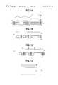
- FIG. 1A-1Hshow steps involved in the formation of an inter-layer dielectric layer according to a preferred embodiment of the invention
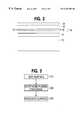
- FIG. 2shows a structure having a fluorinedepleted region that is formed between two conducting layers
- FIG. 3shows the steps involved in creating a fluorine-depleted region on a fluorine-based inter-layer dielectric according to the invention.
- the present inventionwill be described in detail below, with references to the accompanying figures.
- the present inventionis described in the context of use with an inter-layer dielectric layer (ILD) in a conducting stack on a semiconductor chip.
- ILDinter-layer dielectric layer
- the present inventionhas broad application to other structures or devices where a dielectric layer containing fluorine is used as an interlayer dielectric for other kinds of conductive layers.
- FIGS. 1A-1Hillustratively show the steps involved in creating a low-K SiOF (or fluorosilicate glass) as an inter-metal dielectric for a semiconductor device formed on a substrate (e.g., silicon substrate).
- FIG. 1Ashows a first fluorosilicate glass (FSG) layer 20 that has been deposited onto a semiconductor substrate 10 .
- the first FSG layer 20covers metal stacks 30 , 40 , and 50 .
- Each metal stack 30 , 40 , 50may include, for example, a liner 30 A, 40 A, 50 A that is either a Ti or TiN layer, an aluminum (or other type of conductive metal) layer 30 B, 40 B, 50 B, and an anti-reflective coating (ARC) layer 30 C, 40 C, 50 C.
- a liner 30 A, 40 A, 50 Athat is either a Ti or TiN layer
- an aluminum (or other type of conductive metal) layer 30 B, 40 B, 50 Band an anti-reflective coating (ARC) layer 30 C, 40 C, 50 C.
- ARCanti-reflective coating
- the first FSG layer 20is deposited by way of an in-situ gap-fill high density plasma (HDP) process having a high etch/deposition ratio with high bias power.
- HDPuses both an etch element and a deposition element to provide for an etch/deposition process in-situ. Having a high etch/deposition ratio is useful for gap filling, such as between closely-positioned metal stacks on a substrate.
- the first FSG layer 20is preferably deposited using HDP at an etch/deposition ratio of between 0.6 to 0.8.
- the preferred thickness of the first FSG layer 20is in a range of from 0.8 to 1.0 microns. Of course, other thicknesses are possible.
- the function of the first FSG layer 20is usually done in two steps, one step being the formation of a thin (100 to 200 angstrom) FSG layer using a very low bias power (and thus a low etch/deposition ratio), and then a next step being the formation of the rest of the first FSG layer by using a high bias power and high etch/deposition ratio.
- the thin FSG layer that is initially depositedacts as a protection layer for the metal stacks 30 , 40 , 50 that might otherwise by partially etched (and thereby damaged) due to the high bias power used in the later step of forming the bulk of the first FSG layer 20 .
- the thickness of the first FSG layer 20is preferably about 1.2 times the height of the metal stacks 30 , 40 and 50 . Of course, other ratios of first FSG layer/metal stack thickness are possible while remaining within the scope of the invention.
- the first FSG layer 20preferably has a dielectric constant in a range of from 3.5 to 3.8, with the exact value depending upon the amount of fluorine in the first FSG layer 20 .
- a second FSG layer 60is deposited on top of the first FSG layer 20 , as shown in FIG. 1 A.
- the boundary between the first FSG layer 20 and the second FSG layer 60is shown by the dashed line in FIG. 1 A.
- the second FSG layer 60is deposited by way of an in-situ HDP process, similar to the one performed in depositing the first FSG layer 20 , but with a lower etch/deposition ratio.
- the second FSG layer 60is deposited using a lower bias power and thus lower etch/deposition ratio, since, once the gaps between the metal stacks 30 , 40 , 50 are filled by the first FSG layer 20 , a large amount of etch element is no longer needed for gap filling.
- a primarily-deposition processcan be performed in-situ for the forming of the second FSG layer 60 , which provides a higher throughput than that obtained in the formation of the first FSG layer 20 .
- Typical etch/deposition ratios for the second FSG layer 60are in the range of from 0.1 to 0.5.
- the second FSG layermay be formed by PECVD, which has even a higher throughput but requires a different chamber to be used in this alternative way of forming the second FSG layer 60 .
- the etch chemistry to be used in this alternative way of forming the second FSG layer 60is TEOS-based, such as a PE-FTEOS process for forming the second FSG layer 60 .
- the HDP processesuse a silane-based oxide, which is different from TEOS.
- the thickness of the second FSG layer 60is preferably in a range of from one to two times the thickness of the first FSG layer 20 .
- the second FSG layer 60preferably has a dielectric constant in a range of from 3.5 to 3.8.
- FIG. 1Bshows the semiconductor device 5 after a chemical mechanical polishing (CMP) and clean has been performed on the semiconductor device 5 .
- FSG layer 70includes both the first and second FSG layers 20 , 60 of FIG. 1 A.
- the top surface of FSG layer 70is made to have a substantially planar surface.
- the top surface of the FSG layer 70may be planarized by other methods known in the art, such as by an etch back.
- the CMP and clean stepremoves about 0.7 to 1.0 microns of the top portion of the FSG layer 70 , leaving an FSG layer of from 0.8 to 1.0 microns in thickness. Of course, other thicknesses are possible.
- FIG. 1Cshows a step of providing a surface treatment to the FSG layer 70 , in a manner described in a related co-pending U.S. patent application Ser. No. 09/157,240, filed Sep. 18, 1998, now U.S. Pat. No. 5,994,778 which is incorporated in its entirety herein by reference.
- This surface treatment stepinvolves treating the surface of the FSG layer 70 with a plasma containing hydrogen (shown by the downward-pointing arrows in FIG. 1 C).
- the plasmamay be pure hydrogen, or it may be diluted H 2 plasma, such as, for example, an H 2 /N 2 plasma.
- the purpose of the hydrogen plasmais to make the hydrogen less volatile. That is, the activation energy of the hydrogen is too high to bond with the fluorine atoms if it is not in a plasma form.
- the hydrogen in the plasmawill bond with the fluorine atoms in the FSG layer 70 to form HF, which, because of its high vapor pressure and low boiling point, will be vaporized and evacuated from the system, leaving a fluorine depleted region (layer 72 in FIG. 1 D).
- the hydrogen treatmentis performed in a CVD chamber, such as, for example, an Applied Materials CVD chamber.
- the CVD chambermay be the same chamber used to deposit a subsequent conducting layer, such as Ti, TiN, Ta, or TaN.
- the CVD chamber for the hydrogen plasma treatmentshould have a slightly elevated temperature (5-50° C. higher) relative to the temperature used to deposit the subsequent conducting layer. For example, if a temperature falling in the range of 375° C. to 450° C. is to be used to deposit a subsequent conducting layer, then a slightly elevated temperature that is 5-50° C. higher than a conducting layer CVD deposition temperature (performed after the hydrogen plasma treatment) is used during the hydrogen plasma treatment step.
- this elevated temperatureis to lower the probability that heating during the subsequent conducting layer deposition step will drive the fluorine atoms from the bulk FSG layer 71 into the fluorine-depleted region 72 , which are layers that exist after the surface treatment of the FSG layer 70 with hydrogen plasma, as shown in FIG. 1 D.
- the other parameters for the hydrogen plasma treatment stepwill be determined empirically. Typically, the pressure in the CVD chamber will be in the milli-torr to torr range, the energy parameter will be in the several hundred watt range, and plasma treatment time will range from 20 seconds to several minutes. Optimized parameters will be determined based on the desired thickness of the fluorine-depleted region.
- FIG. 1Dalso shows a nitrided region 80 , which is about 50 angstroms in thickness.
- the nitrided region 80acts as a passivation layer, and may be an SiON layer, for example.
- a portion of the depleted region 72is passivated to form the passivation layer 80 , which is less than the thickness of the depleted region 72 .
- One purpose of the passivation layer 80is to bond non-volatile atoms into the depleted region 72 to lessen the probability of fluorine atoms from the bulk FSG layer 71 diffusing up into the depleted region 72 and thereafter reacting with the conducting layer atoms of a subsequently deposited layer.
- the passivation stepmay be carried out by switching to a pure N 2 plasma in a CVD chamber to form SiON to a thickness that is less than the thickness of the depletion region 72 , thereby leaving a passivation layer 80 and fluorine depleted region 72 as shown in FIG. 1 D.
- a higher source powerwill be used in the CVD chamber, for example, 300-400 watts, to cause the nitrogen to bond with the SiO surface to yield an SiON dielectric barrier.
- This passivated dielectric barrier layer 80lessens the potential that fluorine atoms will diffuse up to the surface of the fluorine-depleted region 72 , and thereafter react, for example, with a Ti or TiN barrier metal deposited thereabove.
- a lower bias power(the bias power is different than the plasma power) and a higher pressure condition preferably is used to treat sidewalls and vias in the FSG layer 70 , which are provided for electrical connections to layers below the FSG layer 70 .
- a bias powerof less than 100 watts may be utilized.
- One purpose for the low bias poweris to make the plasma less directional so that it will better affect the sidewalls.
- the fluorine-depleted region 72is about 100 angstroms in thickness
- the nitrided region that forms the passivation layer 80is about 50 angstroms in thickness.
- Other sizesmay be contemplated while remaining within the scope of the invention as described herein.
- the exact thickness of the passivation layer 80may be optimized empirically. A SIMS analysis may be performed to measure the thickness of the fluorine-depleted region 72 and the thickness of the passivation layer 80 . Ultimately, optimization is achieved when the depletion and passivation layer thicknesses are such that it can be assumed that any subsequent layer applied thereto will not peel off during the remaining process steps for creating the semiconductor device on the substrate.
- an oxide cap 90is deposited onto the silicon substrate, as shown in FIG. 1 E.
- the oxide cap 90preferably has a thickness of from 500-2500 angstroms, with the thickness being based on the quality of the oxide cap (e.g., better quality oxide cap means lesser thickness needed).
- the SiO 2 capis preferably deposited by way of PECVD.
- the oxide cap 90can be either SiH 4 or TEOS based, and preferably is an silicon-rich oxide with a reflective index (RI) greater than 1.47. This may be achieved by increasing the silane flow and power during the PECVD process, for example.
- the surface treatment step and the oxide cap stepare performed in-situ to simplify production and to maximize throughput.
- One or more conducting layersmay be provided on top of the oxide cap 90 . These conducting layers are electrically connected to one or all of the metal stacks 30 , 40 , 50 , or to regions in the substrate by virtue of conductive material, such as tungsten, provided in vias formed in the FSG layer 70 .
- the fluorine-depleted region 72 at the top portion of the FSG layer 70lessens the possibility that any fluorine atoms will diffuse up to the conducting layers, and thereby lessening the possibility of forming impurities in those layers.
- the nitride layer 80 and oxide cap 90act a barrier to keep the fluorine atoms in the FSG layer 70 from corrupting the conducting layers.
- FIG. 1Fshows the semiconductor device after vias 150 , 160 have been formed in the FSG layer 70 and the oxide cap 90 .
- Via 150provides an electrical connection to metal stack 30 by virtue of an electrical conductor (e.g., tungsten) provided in the via 150
- via 160provides an electrical connection to metal stack 50 by virtue of an electrical conductor provided in the via 160 .
- Vias 150 , 160may be formed by using a contour mask and an etch using a plasma treatment, in a manner known to those skilled in the art.
- Via 150is shown as being formed offset with respect to the metal stack 10 . This may be an unintentional effect due to, for example, offset in a stepper used in chip manufacturing process.
- viasmay be intentionally formed offset with respect to conducting layers directly above and below the vias, in order to better take advantage of the real estate on a semiconductor chip.
- a barrier metal(Ti or TiN, for example) is deposited in the vias 150 , 160 , to thereby form a thin barrier layer in the vias.
- the sidewall treatment of the viasis discussed above, and is shown in detail in FIG. 1G with respect to via 150 .
- the side surface of via 150 (and also via 160 )has a nitrided region 80 , a fluorine-depleted region 72 , and a bulk FSG region 71 .
- FIG. 1Hshows a conducting layer 250 and a conducting layer 260 that have been formed above the oxide cap 90 .
- an in-situ deposition of optimized CVD-TiNmay be accomplished in the previously-mentioned CVD chamber using a nitrogen-rich initial layer. This deposition would then be followed by a standard blanket tungsten deposition to provide a conducting material in the vias. A tungsten CMP and clean step is then performed after the tungsten has been deposited in the vias.
- Conducting layer 250is electrically connected to metal stack 10 by virtue of the tungsten (of other conductive material) in the via 150
- conducting layer 260is electrically connected to metal stack 30 by virtue of the tungsten (or other conductive material) in the via 160
- FSG layer 70provides for electrical separation between components above and below that layer, and allows for electrical connections to those layers by way of vias formed in the FSG layer 70 .
- FSG layer 70may be formed between a metal-2 layer and a metal-3 layer, or between a metal-3 layer and a metal-4 layer, etc.
- FIG. 2shows a structure having a bulk substrate 12 , a first conducting layer 14 formed on the substrate 12 , a SiOF layer 16 that is formed on the first conducting layer 14 and that includes a depleted layer 18 and an SiON passivation layer 21 , a second conducting layer 22 formed on the passivation layer 21 , and a tungsten-deposition layer 24 formed on the conducting layer 22 .
- FIG. 2is taken from the related U.S. patent application 09/157,240, discussed above.
- FIG. 3is also taken from the related U.S. patent application Ser. No. 09/157,240, and shows the three steps involved in creating a fluorine-depleted region.
- a first step 310an SiOF layer or other type of fluorine-based layer is deposited. Then, in a step 320 , either H 2 or H 2 /N 2 plasma treatment is performed, to thereby create a fluorine-depleted region 18 in the SiOF layer. Next, in a step 330 , the surface of the fluorine-depleted region 18 is passivated with a nitrogen-rich plasma to form a passivation layer 20 .
- the passivation layer 20provides additional protection in keeping fluorine atoms in the SiOF layer from moving into a conducting layer formed above the SiOF layer.
- the present inventionis particularly advantageous when used to form an SiOF (or FSG) inter-metal dielectric layer, it has application in any situation where the fluorine atoms in an inter-metal dielectric are causing interaction and/or adhesion problems with other neighboring layers.
- a substratemay generally be defined as any layer or material which lies underneath and supports the inter-layer dielectric.
- the present inventionhas been described with respect to a metal stack that corresponds to a metal-1 layer.
- the present inventionis applicable to the protection of any kind of conducting layer besides a metal stack.
- the present inventionha been described with respect to a two-step formation of an FSG layer.
- One of ordinary skill in the artwill recognize that the formation of a fluorine-depleted region, a nitrided region, and an oxide cap according to the present invention may be done no matter how the FSG layer was formed on a substrate (e.g., one-step process for forming an FSG layer).
Landscapes
- Engineering & Computer Science (AREA)
- Physics & Mathematics (AREA)
- Condensed Matter Physics & Semiconductors (AREA)
- General Physics & Mathematics (AREA)
- Computer Hardware Design (AREA)
- Microelectronics & Electronic Packaging (AREA)
- Power Engineering (AREA)
- Manufacturing & Machinery (AREA)
- Plasma & Fusion (AREA)
- Internal Circuitry In Semiconductor Integrated Circuit Devices (AREA)
Abstract
Description
Claims (4)
Priority Applications (5)
| Application Number | Priority Date | Filing Date | Title |
|---|---|---|---|
| US09/203,572US6252303B1 (en) | 1998-12-02 | 1998-12-02 | Intergration of low-K SiOF as inter-layer dielectric |
| US09/373,483US6444593B1 (en) | 1998-12-02 | 1999-08-12 | Surface treatment of low-K SiOF to prevent metal interaction |
| US09/373,482US6281584B1 (en) | 1998-12-02 | 1999-08-12 | Integrated circuit with improved adhesion between interfaces of conductive and dielectric surfaces |
| US09/765,666US6400023B2 (en) | 1998-12-02 | 2001-01-22 | Integration of low-k SiOF for damascene structure |
| US09/886,032US6489230B1 (en) | 1998-12-02 | 2001-06-22 | Integration of low-k SiOF as inter-layer dielectric |
Applications Claiming Priority (1)
| Application Number | Priority Date | Filing Date | Title |
|---|---|---|---|
| US09/203,572US6252303B1 (en) | 1998-12-02 | 1998-12-02 | Intergration of low-K SiOF as inter-layer dielectric |
Related Child Applications (4)
| Application Number | Title | Priority Date | Filing Date |
|---|---|---|---|
| US09/373,483Continuation-In-PartUS6444593B1 (en) | 1998-12-02 | 1999-08-12 | Surface treatment of low-K SiOF to prevent metal interaction |
| US09/373,482Continuation-In-PartUS6281584B1 (en) | 1998-12-02 | 1999-08-12 | Integrated circuit with improved adhesion between interfaces of conductive and dielectric surfaces |
| US09/765,666DivisionUS6400023B2 (en) | 1998-12-02 | 2001-01-22 | Integration of low-k SiOF for damascene structure |
| US09/886,032DivisionUS6489230B1 (en) | 1998-12-02 | 2001-06-22 | Integration of low-k SiOF as inter-layer dielectric |
Publications (1)
| Publication Number | Publication Date |
|---|---|
| US6252303B1true US6252303B1 (en) | 2001-06-26 |
Family
ID=22754527
Family Applications (3)
| Application Number | Title | Priority Date | Filing Date |
|---|---|---|---|
| US09/203,572Expired - LifetimeUS6252303B1 (en) | 1998-12-02 | 1998-12-02 | Intergration of low-K SiOF as inter-layer dielectric |
| US09/765,666Expired - LifetimeUS6400023B2 (en) | 1998-12-02 | 2001-01-22 | Integration of low-k SiOF for damascene structure |
| US09/886,032Expired - Fee RelatedUS6489230B1 (en) | 1998-12-02 | 2001-06-22 | Integration of low-k SiOF as inter-layer dielectric |
Family Applications After (2)
| Application Number | Title | Priority Date | Filing Date |
|---|---|---|---|
| US09/765,666Expired - LifetimeUS6400023B2 (en) | 1998-12-02 | 2001-01-22 | Integration of low-k SiOF for damascene structure |
| US09/886,032Expired - Fee RelatedUS6489230B1 (en) | 1998-12-02 | 2001-06-22 | Integration of low-k SiOF as inter-layer dielectric |
Country Status (1)
| Country | Link |
|---|---|
| US (3) | US6252303B1 (en) |
Cited By (19)
| Publication number | Priority date | Publication date | Assignee | Title |
|---|---|---|---|---|
| US20010017402A1 (en)* | 2000-02-10 | 2001-08-30 | Tatsuya Usami | Semiconductor device and method of manufacturing the same |
| WO2002013234A3 (en)* | 2000-08-04 | 2002-08-01 | Applied Materials Inc | Stabilized surface between a fluorosilicate glass dielectric and a liner/barrier layer |
| US6444593B1 (en) | 1998-12-02 | 2002-09-03 | Advanced Micro Devices, Inc. | Surface treatment of low-K SiOF to prevent metal interaction |
| US20030057553A1 (en)* | 2000-04-03 | 2003-03-27 | Delarosa Mark J. | Fluorine diffusion barriers for fluorinated dielectrics in integrated circuits |
| US20030235994A1 (en)* | 2002-06-20 | 2003-12-25 | Taiwan Semiconductor Manufacturing Co., Ltd. | Method of avoiding plasma arcing during RIE etching |
| US6713831B1 (en)* | 2001-12-04 | 2004-03-30 | Cypress Semiconductor Corp. | Borderless contact architecture |
| US6727588B1 (en)* | 1999-08-19 | 2004-04-27 | Agere Systems Inc. | Diffusion preventing barrier layer in integrated circuit inter-metal layer dielectrics |
| US6794295B1 (en)* | 2000-05-26 | 2004-09-21 | Taiwan Semiconductor Manufacturing Company, Ltd. | Method to improve stability and reliability of CVD low K dielectric |
| US20040264641A1 (en)* | 2003-06-27 | 2004-12-30 | Samsung Electronics Co., Ltd. | Apparatus for measuring energy resolving power of X-ray monochromator and solid sample using in the same |
| US8771491B2 (en) | 2009-09-30 | 2014-07-08 | Quantapore, Inc. | Ultrafast sequencing of biological polymers using a labeled nanopore |
| WO2014190322A2 (en) | 2013-05-24 | 2014-11-27 | Quantapore, Inc. | Nanopore-based nucleic acid analysis with mixed fret detection |
| WO2016057829A1 (en) | 2014-10-10 | 2016-04-14 | Quantapore, Inc. | Nanopore-based polymer analysis with mutually-quenching fluorescent labels |
| US9624537B2 (en) | 2014-10-24 | 2017-04-18 | Quantapore, Inc. | Efficient optical analysis of polymers using arrays of nanostructures |
| US9651539B2 (en) | 2012-10-28 | 2017-05-16 | Quantapore, Inc. | Reducing background fluorescence in MEMS materials by low energy ion beam treatment |
| WO2017100027A1 (en) | 2015-12-08 | 2017-06-15 | Quantapore, Inc. | Method of translocating nucleic acids through nanopores |
| WO2017123647A1 (en) | 2016-01-15 | 2017-07-20 | Quantapore, Inc. | Optically-based nanopore analysis with reduced background |
| WO2017209891A1 (en) | 2016-05-31 | 2017-12-07 | Quantapore, Inc. | Two-color nanopore sequencing |
| US9903820B2 (en) | 2007-05-08 | 2018-02-27 | The Trustees Of Boston University | Chemical functionalization of solid-state nanopores and nanopore arrays and applications thereof |
| US10823721B2 (en) | 2016-07-05 | 2020-11-03 | Quantapore, Inc. | Optically based nanopore sequencing |
Families Citing this family (25)
| Publication number | Priority date | Publication date | Assignee | Title |
|---|---|---|---|---|
| FR2798512B1 (en)* | 1999-09-14 | 2001-10-19 | Commissariat Energie Atomique | PROCESS FOR MAKING A COPPER CONNECTION THROUGH A DIELECTRIC MATERIAL LAYER OF AN INTEGRATED CIRCUIT |
| KR100346843B1 (en)* | 2000-12-07 | 2002-08-03 | 삼성전자 주식회사 | Method of forming interlayer dielectric film and method of manufacturing semiconductor device |
| TW465042B (en)* | 2001-01-29 | 2001-11-21 | Macronix Int Co Ltd | Method for forming metal/dielectric multi-level connects |
| US7001854B1 (en) | 2001-08-03 | 2006-02-21 | Novellus Systems, Inc. | Hydrogen-based phosphosilicate glass process for gap fill of high aspect ratio structures |
| US6846745B1 (en)* | 2001-08-03 | 2005-01-25 | Novellus Systems, Inc. | High-density plasma process for filling high aspect ratio structures |
| JP4257051B2 (en)* | 2001-08-10 | 2009-04-22 | 株式会社ルネサステクノロジ | Manufacturing method of semiconductor integrated circuit device |
| DE10141352A1 (en)* | 2001-08-23 | 2003-06-05 | Osram Opto Semiconductors Gmbh | Process for the surface treatment of a semiconductor |
| US7067440B1 (en) | 2001-08-24 | 2006-06-27 | Novellus Systems, Inc. | Gap fill for high aspect ratio structures |
| JP2003068850A (en)* | 2001-08-29 | 2003-03-07 | Tokyo Electron Ltd | Semiconductor device and method of manufacturing the same |
| US6586347B1 (en)* | 2001-10-16 | 2003-07-01 | Taiwan Semiconductor Manufacturing Company | Method and structure to improve the reliability of multilayer structures of FSG (F-doped SiO2) dielectric layers and metal layers in semiconductor integrated circuits |
| US7101788B2 (en)* | 2002-02-28 | 2006-09-05 | Texas Instruments Incorporated | Semiconductor devices and methods of manufacturing such semiconductor devices |
| US6828255B2 (en)* | 2002-11-22 | 2004-12-07 | Taiwan Semiconductor Manufacturing Co., Ltd | Crack inhibited composite dielectric layer |
| US7122485B1 (en) | 2002-12-09 | 2006-10-17 | Novellus Systems, Inc. | Deposition profile modification through process chemistry |
| US6924242B2 (en)* | 2003-10-23 | 2005-08-02 | Taiwan Semiconductor Manufacturing Company, Ltd. | SiOC properties and its uniformity in bulk for damascene applications |
| US7344996B1 (en) | 2005-06-22 | 2008-03-18 | Novellus Systems, Inc. | Helium-based etch process in deposition-etch-deposition gap fill |
| US7163896B1 (en) | 2003-12-10 | 2007-01-16 | Novellus Systems, Inc. | Biased H2 etch process in deposition-etch-deposition gap fill |
| US7476621B1 (en) | 2003-12-10 | 2009-01-13 | Novellus Systems, Inc. | Halogen-free noble gas assisted H2 plasma etch process in deposition-etch-deposition gap fill |
| US7217658B1 (en) | 2004-09-07 | 2007-05-15 | Novellus Systems, Inc. | Process modulation to prevent structure erosion during gap fill |
| US7176039B1 (en) | 2004-09-21 | 2007-02-13 | Novellus Systems, Inc. | Dynamic modification of gap fill process characteristics |
| US7381451B1 (en) | 2004-11-17 | 2008-06-03 | Novellus Systems, Inc. | Strain engineering—HDP thin film with tensile stress for FEOL and other applications |
| US7271110B2 (en)* | 2005-01-05 | 2007-09-18 | Chartered Semiconductor Manufacturing, Ltd. | High density plasma and bias RF power process to make stable FSG with less free F and SiN with less H to enhance the FSG/SiN integration reliability |
| US7211525B1 (en) | 2005-03-16 | 2007-05-01 | Novellus Systems, Inc. | Hydrogen treatment enhanced gap fill |
| US7482245B1 (en) | 2006-06-20 | 2009-01-27 | Novellus Systems, Inc. | Stress profile modulation in STI gap fill |
| KR100835423B1 (en)* | 2006-08-29 | 2008-06-04 | 동부일렉트로닉스 주식회사 | Dual damascene pattern formation method in semiconductor manufacturing process |
| US8133797B2 (en)* | 2008-05-16 | 2012-03-13 | Novellus Systems, Inc. | Protective layer to enable damage free gap fill |
Citations (5)
| Publication number | Priority date | Publication date | Assignee | Title |
|---|---|---|---|---|
| US5807785A (en)* | 1996-08-02 | 1998-09-15 | Applied Materials, Inc. | Low dielectric constant silicon dioxide sandwich layer |
| US5896149A (en)* | 1995-06-12 | 1999-04-20 | Seiko Epson Corporation | Ink jet type recording head having a flow passage substrate with a stepped configuration and recesses formed in a surface thereof |
| US6008120A (en)* | 1998-07-22 | 1999-12-28 | Siemens Aktiengesellschaft | Silicon oxynitride cap for fluorinated silicate glass film in intermetal dielectric semiconductor fabrication |
| US6051321A (en)* | 1997-10-24 | 2000-04-18 | Quester Technology, Inc. | Low dielectric constant materials and method |
| US6070550A (en)* | 1996-09-12 | 2000-06-06 | Applied Materials, Inc. | Apparatus for the stabilization of halogen-doped films through the use of multiple sealing layers |
Family Cites Families (8)
| Publication number | Priority date | Publication date | Assignee | Title |
|---|---|---|---|---|
| JP3979687B2 (en)* | 1995-10-26 | 2007-09-19 | アプライド マテリアルズ インコーポレイテッド | Method for improving film stability of halogen-doped silicon oxide films |
| US5763010A (en)* | 1996-05-08 | 1998-06-09 | Applied Materials, Inc. | Thermal post-deposition treatment of halogen-doped films to improve film stability and reduce halogen migration to interconnect layers |
| US5989998A (en) | 1996-08-29 | 1999-11-23 | Matsushita Electric Industrial Co., Ltd. | Method of forming interlayer insulating film |
| JP3019021B2 (en)* | 1997-03-31 | 2000-03-13 | 日本電気株式会社 | Semiconductor device and manufacturing method thereof |
| US6136685A (en)* | 1997-06-03 | 2000-10-24 | Applied Materials, Inc. | High deposition rate recipe for low dielectric constant films |
| US5920790A (en) | 1997-08-29 | 1999-07-06 | Motorola, Inc. | Method of forming a semiconductor device having dual inlaid structure |
| US5994997A (en)* | 1997-11-24 | 1999-11-30 | Motorola, Inc. | Thick-film resistor having concentric terminals and method therefor |
| US5994778A (en) | 1998-09-18 | 1999-11-30 | Advanced Micro Devices, Inc. | Surface treatment of low-k SiOF to prevent metal interaction |
- 1998
- 1998-12-02USUS09/203,572patent/US6252303B1/ennot_activeExpired - Lifetime
- 2001
- 2001-01-22USUS09/765,666patent/US6400023B2/ennot_activeExpired - Lifetime
- 2001-06-22USUS09/886,032patent/US6489230B1/ennot_activeExpired - Fee Related
Patent Citations (5)
| Publication number | Priority date | Publication date | Assignee | Title |
|---|---|---|---|---|
| US5896149A (en)* | 1995-06-12 | 1999-04-20 | Seiko Epson Corporation | Ink jet type recording head having a flow passage substrate with a stepped configuration and recesses formed in a surface thereof |
| US5807785A (en)* | 1996-08-02 | 1998-09-15 | Applied Materials, Inc. | Low dielectric constant silicon dioxide sandwich layer |
| US6070550A (en)* | 1996-09-12 | 2000-06-06 | Applied Materials, Inc. | Apparatus for the stabilization of halogen-doped films through the use of multiple sealing layers |
| US6051321A (en)* | 1997-10-24 | 2000-04-18 | Quester Technology, Inc. | Low dielectric constant materials and method |
| US6008120A (en)* | 1998-07-22 | 1999-12-28 | Siemens Aktiengesellschaft | Silicon oxynitride cap for fluorinated silicate glass film in intermetal dielectric semiconductor fabrication |
Cited By (29)
| Publication number | Priority date | Publication date | Assignee | Title |
|---|---|---|---|---|
| US6444593B1 (en) | 1998-12-02 | 2002-09-03 | Advanced Micro Devices, Inc. | Surface treatment of low-K SiOF to prevent metal interaction |
| US6727588B1 (en)* | 1999-08-19 | 2004-04-27 | Agere Systems Inc. | Diffusion preventing barrier layer in integrated circuit inter-metal layer dielectrics |
| US6670709B2 (en)* | 2000-02-10 | 2003-12-30 | Nec Electronics Corporation | Semiconductor device and method of manufacturing the same |
| US20010017402A1 (en)* | 2000-02-10 | 2001-08-30 | Tatsuya Usami | Semiconductor device and method of manufacturing the same |
| US6818990B2 (en)* | 2000-04-03 | 2004-11-16 | Rensselaer Polytechnic Institute | Fluorine diffusion barriers for fluorinated dielectrics in integrated circuits |
| US20030057553A1 (en)* | 2000-04-03 | 2003-03-27 | Delarosa Mark J. | Fluorine diffusion barriers for fluorinated dielectrics in integrated circuits |
| US6794295B1 (en)* | 2000-05-26 | 2004-09-21 | Taiwan Semiconductor Manufacturing Company, Ltd. | Method to improve stability and reliability of CVD low K dielectric |
| WO2002013234A3 (en)* | 2000-08-04 | 2002-08-01 | Applied Materials Inc | Stabilized surface between a fluorosilicate glass dielectric and a liner/barrier layer |
| US6713831B1 (en)* | 2001-12-04 | 2004-03-30 | Cypress Semiconductor Corp. | Borderless contact architecture |
| US20030235994A1 (en)* | 2002-06-20 | 2003-12-25 | Taiwan Semiconductor Manufacturing Co., Ltd. | Method of avoiding plasma arcing during RIE etching |
| US7247252B2 (en)* | 2002-06-20 | 2007-07-24 | Taiwan Semiconductor Manufacturing Co., Ltd. | Method of avoiding plasma arcing during RIE etching |
| US20040264641A1 (en)* | 2003-06-27 | 2004-12-30 | Samsung Electronics Co., Ltd. | Apparatus for measuring energy resolving power of X-ray monochromator and solid sample using in the same |
| US9903820B2 (en) | 2007-05-08 | 2018-02-27 | The Trustees Of Boston University | Chemical functionalization of solid-state nanopores and nanopore arrays and applications thereof |
| US11002724B2 (en) | 2007-05-08 | 2021-05-11 | Trustees Of Boston University | Chemical functionalization of solid-state nanopores and nanopore arrays and applications thereof |
| US10101315B2 (en) | 2007-05-08 | 2018-10-16 | Trustees Of Boston University | Chemical functionalization of solid-state nanopores and nanopore arrays and applications thereof |
| US9279153B2 (en) | 2009-09-30 | 2016-03-08 | Quantapore, Inc. | Ultrafast sequencing of biological polymers using a labeled nanopore |
| US8771491B2 (en) | 2009-09-30 | 2014-07-08 | Quantapore, Inc. | Ultrafast sequencing of biological polymers using a labeled nanopore |
| US9651539B2 (en) | 2012-10-28 | 2017-05-16 | Quantapore, Inc. | Reducing background fluorescence in MEMS materials by low energy ion beam treatment |
| US9862997B2 (en) | 2013-05-24 | 2018-01-09 | Quantapore, Inc. | Nanopore-based nucleic acid analysis with mixed FRET detection |
| WO2014190322A2 (en) | 2013-05-24 | 2014-11-27 | Quantapore, Inc. | Nanopore-based nucleic acid analysis with mixed fret detection |
| US10597712B2 (en) | 2014-10-10 | 2020-03-24 | Quantapore, Inc. | Nanopore-based polymer analysis with mutually-quenching fluorescent labels |
| US9885079B2 (en) | 2014-10-10 | 2018-02-06 | Quantapore, Inc. | Nanopore-based polymer analysis with mutually-quenching fluorescent labels |
| WO2016057829A1 (en) | 2014-10-10 | 2016-04-14 | Quantapore, Inc. | Nanopore-based polymer analysis with mutually-quenching fluorescent labels |
| US9624537B2 (en) | 2014-10-24 | 2017-04-18 | Quantapore, Inc. | Efficient optical analysis of polymers using arrays of nanostructures |
| US11041197B2 (en) | 2014-10-24 | 2021-06-22 | Quantapore, Inc. | Efficient optical analysis of polymers using arrays of nanostructures |
| WO2017100027A1 (en) | 2015-12-08 | 2017-06-15 | Quantapore, Inc. | Method of translocating nucleic acids through nanopores |
| WO2017123647A1 (en) | 2016-01-15 | 2017-07-20 | Quantapore, Inc. | Optically-based nanopore analysis with reduced background |
| WO2017209891A1 (en) | 2016-05-31 | 2017-12-07 | Quantapore, Inc. | Two-color nanopore sequencing |
| US10823721B2 (en) | 2016-07-05 | 2020-11-03 | Quantapore, Inc. | Optically based nanopore sequencing |
Also Published As
| Publication number | Publication date |
|---|---|
| US6489230B1 (en) | 2002-12-03 |
| US20010016419A1 (en) | 2001-08-23 |
| US6400023B2 (en) | 2002-06-04 |
Similar Documents
| Publication | Publication Date | Title |
|---|---|---|
| US6252303B1 (en) | Intergration of low-K SiOF as inter-layer dielectric | |
| US6177364B1 (en) | Integration of low-K SiOF for damascene structure | |
| US6074942A (en) | Method for forming a dual damascene contact and interconnect | |
| US7888741B2 (en) | Structures with improved interfacial strength of SiCOH dielectrics and method for preparing the same | |
| US7030023B2 (en) | Method for simultaneous degas and baking in copper damascene process | |
| US5716890A (en) | Structure and method for fabricating an interlayer insulating film | |
| US6800940B2 (en) | Low k dielectric composite layer for integrated circuit structure which provides void-free low k dielectric material between metal lines while mitigating via poisoning | |
| US20020135040A1 (en) | Integrated circuit structure having low dielectric constant material and having silicon oxynitride caps over closely spaced apart metal lines | |
| US6004876A (en) | Low resistance interconnect for a semiconductor device and method of fabricating the same | |
| US6335273B2 (en) | Surface treatment of low-K SiOF to prevent metal interaction | |
| US6433433B1 (en) | Semiconductor device with misaligned via hole | |
| US6495448B1 (en) | Dual damascene process | |
| US7335598B2 (en) | Chemical-mechanical polishing method | |
| US6048788A (en) | Method of fabricating metal plug | |
| US6562725B2 (en) | Dual damascene structure employing nitrogenated silicon carbide and non-nitrogenated silicon carbide etch stop layers | |
| US6207567B1 (en) | Fabricating method of glue layer and barrier layer | |
| US7030044B2 (en) | Method of forming a cap layer having anti-reflective characteristics on top of a low-k dielectric | |
| US6440838B1 (en) | Dual damascene structure employing laminated intermediate etch stop layer | |
| US7351653B2 (en) | Method for damascene process | |
| US6444593B1 (en) | Surface treatment of low-K SiOF to prevent metal interaction | |
| JP2001118928A (en) | Manufacturing method of integrated circuit | |
| JP2000200786A (en) | Method of forming insulating film | |
| US6281584B1 (en) | Integrated circuit with improved adhesion between interfaces of conductive and dielectric surfaces | |
| JP2001144180A (en) | Multilayer wiring structure and manufacturing method therefor | |
| US6171963B1 (en) | Method for forming a planar intermetal dielectric using a barrier layer |
Legal Events
| Date | Code | Title | Description |
|---|---|---|---|
| AS | Assignment | Owner name:ADVANCED MICRO DEVICES, INC., CALIFORNIA Free format text:ASSIGNMENT OF ASSIGNORS INTEREST;ASSIGNOR:HUANG, RICHARD J.;REEL/FRAME:009632/0120 Effective date:19981125 | |
| STCF | Information on status: patent grant | Free format text:PATENTED CASE | |
| FPAY | Fee payment | Year of fee payment:4 | |
| FEPP | Fee payment procedure | Free format text:PAYOR NUMBER ASSIGNED (ORIGINAL EVENT CODE: ASPN); ENTITY STATUS OF PATENT OWNER: LARGE ENTITY | |
| FPAY | Fee payment | Year of fee payment:8 | |
| AS | Assignment | Owner name:GLOBALFOUNDRIES INC., CAYMAN ISLANDS Free format text:AFFIRMATION OF PATENT ASSIGNMENT;ASSIGNOR:ADVANCED MICRO DEVICES, INC.;REEL/FRAME:023119/0083 Effective date:20090630 | |
| FPAY | Fee payment | Year of fee payment:12 | |
| AS | Assignment | Owner name:WILMINGTON TRUST, NATIONAL ASSOCIATION, DELAWARE Free format text:SECURITY AGREEMENT;ASSIGNOR:GLOBALFOUNDRIES INC.;REEL/FRAME:049490/0001 Effective date:20181127 | |
| AS | Assignment | Owner name:GLOBALFOUNDRIES INC., CAYMAN ISLANDS Free format text:RELEASE BY SECURED PARTY;ASSIGNOR:WILMINGTON TRUST, NATIONAL ASSOCIATION;REEL/FRAME:054636/0001 Effective date:20201117 | |
| AS | Assignment | Owner name:GLOBALFOUNDRIES U.S. INC., NEW YORK Free format text:RELEASE BY SECURED PARTY;ASSIGNOR:WILMINGTON TRUST, NATIONAL ASSOCIATION;REEL/FRAME:056987/0001 Effective date:20201117 |