US6250192B1 - Method for sawing wafers employing multiple indexing techniques for multiple die dimensions - Google Patents
Method for sawing wafers employing multiple indexing techniques for multiple die dimensionsDownload PDFInfo
- Publication number
- US6250192B1 US6250192B1US08/747,299US74729996AUS6250192B1US 6250192 B1US6250192 B1US 6250192B1US 74729996 AUS74729996 AUS 74729996AUS 6250192 B1US6250192 B1US 6250192B1
- Authority
- US
- United States
- Prior art keywords
- wafer
- saw
- saw blades
- blade
- blades
- Prior art date
- Legal status (The legal status is an assumption and is not a legal conclusion. Google has not performed a legal analysis and makes no representation as to the accuracy of the status listed.)
- Expired - Lifetime
Links
Images


Classifications
- H—ELECTRICITY
- H01—ELECTRIC ELEMENTS
- H01L—SEMICONDUCTOR DEVICES NOT COVERED BY CLASS H10
- H01L21/00—Processes or apparatus adapted for the manufacture or treatment of semiconductor or solid state devices or of parts thereof
- H01L21/67—Apparatus specially adapted for handling semiconductor or electric solid state devices during manufacture or treatment thereof; Apparatus specially adapted for handling wafers during manufacture or treatment of semiconductor or electric solid state devices or components ; Apparatus not specifically provided for elsewhere
- H01L21/67005—Apparatus not specifically provided for elsewhere
- H01L21/67011—Apparatus for manufacture or treatment
- H01L21/67092—Apparatus for mechanical treatment
- B—PERFORMING OPERATIONS; TRANSPORTING
- B28—WORKING CEMENT, CLAY, OR STONE
- B28D—WORKING STONE OR STONE-LIKE MATERIALS
- B28D5/00—Fine working of gems, jewels, crystals, e.g. of semiconductor material; apparatus or devices therefor
- B28D5/02—Fine working of gems, jewels, crystals, e.g. of semiconductor material; apparatus or devices therefor by rotary tools, e.g. drills
- B28D5/022—Fine working of gems, jewels, crystals, e.g. of semiconductor material; apparatus or devices therefor by rotary tools, e.g. drills by cutting with discs or wheels
- B28D5/024—Fine working of gems, jewels, crystals, e.g. of semiconductor material; apparatus or devices therefor by rotary tools, e.g. drills by cutting with discs or wheels with the stock carried by a movable support for feeding stock into engagement with the cutting blade, e.g. stock carried by a pivoted arm or a carriage
- B—PERFORMING OPERATIONS; TRANSPORTING
- B28—WORKING CEMENT, CLAY, OR STONE
- B28D—WORKING STONE OR STONE-LIKE MATERIALS
- B28D5/00—Fine working of gems, jewels, crystals, e.g. of semiconductor material; apparatus or devices therefor
- B28D5/02—Fine working of gems, jewels, crystals, e.g. of semiconductor material; apparatus or devices therefor by rotary tools, e.g. drills
- B28D5/022—Fine working of gems, jewels, crystals, e.g. of semiconductor material; apparatus or devices therefor by rotary tools, e.g. drills by cutting with discs or wheels
- B28D5/029—Fine working of gems, jewels, crystals, e.g. of semiconductor material; apparatus or devices therefor by rotary tools, e.g. drills by cutting with discs or wheels with a plurality of cutting blades
- Y—GENERAL TAGGING OF NEW TECHNOLOGICAL DEVELOPMENTS; GENERAL TAGGING OF CROSS-SECTIONAL TECHNOLOGIES SPANNING OVER SEVERAL SECTIONS OF THE IPC; TECHNICAL SUBJECTS COVERED BY FORMER USPC CROSS-REFERENCE ART COLLECTIONS [XRACs] AND DIGESTS
- Y10—TECHNICAL SUBJECTS COVERED BY FORMER USPC
- Y10T—TECHNICAL SUBJECTS COVERED BY FORMER US CLASSIFICATION
- Y10T83/00—Cutting
- Y10T83/02—Other than completely through work thickness
- Y10T83/0207—Other than completely through work thickness or through work presented
- Y10T83/0215—Including use of rotary scoring blade
- Y10T83/0222—Plural independent rotary scoring blades
- Y—GENERAL TAGGING OF NEW TECHNOLOGICAL DEVELOPMENTS; GENERAL TAGGING OF CROSS-SECTIONAL TECHNOLOGIES SPANNING OVER SEVERAL SECTIONS OF THE IPC; TECHNICAL SUBJECTS COVERED BY FORMER USPC CROSS-REFERENCE ART COLLECTIONS [XRACs] AND DIGESTS
- Y10—TECHNICAL SUBJECTS COVERED BY FORMER USPC
- Y10T—TECHNICAL SUBJECTS COVERED BY FORMER US CLASSIFICATION
- Y10T83/00—Cutting
- Y10T83/02—Other than completely through work thickness
- Y10T83/0333—Scoring
- Y10T83/0363—Plural independent scoring blades
- Y—GENERAL TAGGING OF NEW TECHNOLOGICAL DEVELOPMENTS; GENERAL TAGGING OF CROSS-SECTIONAL TECHNOLOGIES SPANNING OVER SEVERAL SECTIONS OF THE IPC; TECHNICAL SUBJECTS COVERED BY FORMER USPC CROSS-REFERENCE ART COLLECTIONS [XRACs] AND DIGESTS
- Y10—TECHNICAL SUBJECTS COVERED BY FORMER USPC
- Y10T—TECHNICAL SUBJECTS COVERED BY FORMER US CLASSIFICATION
- Y10T83/00—Cutting
- Y10T83/04—Processes
- Y10T83/0524—Plural cutting steps
- Y—GENERAL TAGGING OF NEW TECHNOLOGICAL DEVELOPMENTS; GENERAL TAGGING OF CROSS-SECTIONAL TECHNOLOGIES SPANNING OVER SEVERAL SECTIONS OF THE IPC; TECHNICAL SUBJECTS COVERED BY FORMER USPC CROSS-REFERENCE ART COLLECTIONS [XRACs] AND DIGESTS
- Y10—TECHNICAL SUBJECTS COVERED BY FORMER USPC
- Y10T—TECHNICAL SUBJECTS COVERED BY FORMER US CLASSIFICATION
- Y10T83/00—Cutting
- Y10T83/768—Rotatable disc tool pair or tool and carrier
- Y10T83/7684—With means to support work relative to tool[s]
- Y10T83/7722—Support and tool relatively adjustable
- Y10T83/7726—By movement of the tool
- Y—GENERAL TAGGING OF NEW TECHNOLOGICAL DEVELOPMENTS; GENERAL TAGGING OF CROSS-SECTIONAL TECHNOLOGIES SPANNING OVER SEVERAL SECTIONS OF THE IPC; TECHNICAL SUBJECTS COVERED BY FORMER USPC CROSS-REFERENCE ART COLLECTIONS [XRACs] AND DIGESTS
- Y10—TECHNICAL SUBJECTS COVERED BY FORMER USPC
- Y10T—TECHNICAL SUBJECTS COVERED BY FORMER US CLASSIFICATION
- Y10T83/00—Cutting
- Y10T83/768—Rotatable disc tool pair or tool and carrier
- Y10T83/7809—Tool pair comprises rotatable tools
- Y—GENERAL TAGGING OF NEW TECHNOLOGICAL DEVELOPMENTS; GENERAL TAGGING OF CROSS-SECTIONAL TECHNOLOGIES SPANNING OVER SEVERAL SECTIONS OF THE IPC; TECHNICAL SUBJECTS COVERED BY FORMER USPC CROSS-REFERENCE ART COLLECTIONS [XRACs] AND DIGESTS
- Y10—TECHNICAL SUBJECTS COVERED BY FORMER USPC
- Y10T—TECHNICAL SUBJECTS COVERED BY FORMER US CLASSIFICATION
- Y10T83/00—Cutting
- Y10T83/768—Rotatable disc tool pair or tool and carrier
- Y10T83/7868—Tool element selectively operative
Definitions
- This inventionrelates generally to a method and apparatus for sawing semiconductor substrates such as wafers and, more specifically, to a wafer saw and method of using the same employing multiple indexing techniques and multiple blades for more efficient sawing and for sawing multiple die sizes and shapes from a single semiconductor wafer.
- An individual integrated circuit or chipis usually formed from a larger structure known as a semiconductor wafer, which is usually comprised primarily of silicon, although other materials such as gallium arsenide and indium phosphide are also sometimes used.
- a semiconductor waferhas a plurality of integrated circuits arranged in rows and columns with the periphery of each integrated circuit being rectangular.
- the waferis sawn or “diced” into rectangularly shaped discrete integrated circuits along two mutually perpendicular sets of parallel lines or streets lying between each of the rows and columns thereof.
- the separated or singulated integrated circuitsare commonly referred to as dice.
- One exemplary wafer sawincludes a rotating dicing blade mounted to an aluminum hub and attached to a rotating spindle, the spindle being connected to a motor. Cutting action of the blade may be effected by diamond particles bonded thereto, or a traditional “toothed” type blade may be employed. Many rotating wafer saw blade structures are known in the art. The present invention is applicable to any saw blade construction, so further structures will not be described herein.
- a typical wafer sawing operationincludes attaching the semiconductor wafer to a wafer saw carrier, mechanically, adhesively or otherwise, as known in the art, and mounting the wafer saw carrier on the table of the wafer saw.
- a blade of the wafer sawis passed through the surface of the semiconductor wafer, either by moving the blade relative to the wafer, the table of the saw and the wafer relative to a stationary blade, or a combination of both.
- the bladecuts precisely along each street, returning back over (but not in contact with) the wafer while the wafer is laterally indexed to the next cutting location.
- each pass of the wafer saw bladeis incrementally indexed one unit (a unit being equal to the distance from one street to the next) in a particular orientation of the wafer.
- the wafer saw and the software controlling itare designed to provide uniform and precise indexing in fixed increments across the surface of a wafer.
- a semiconductor wafer having various integrated circuits and other semiconductor devices thereoneach of which may be of a different size.
- RFIDradio-frequency ID
- a battery, chip and antennacould be incorporated into the same wafer such that all semiconductor devices of an RFID electronic device are fabricated from a single semiconductor wafer.
- memory dice of different capacitiesfor example, 4, 16 and 64 megabyte DRAMs, might be fabricated on a single wafer to maximize the use of silicon “real estate” and reduce thiefage or waste of material near the periphery of the almost-circular (but for the flat) wafer.
- an apparatus and method for sawing semiconductor wafersincluding wafers having a plurality of semiconductor devices of different sizes and/or shapes therein.
- the present inventionprovides a wafer saw and method of using the same capable of “multiple indexing” of a wafer saw blade or blades to provide the desired cutting capabilities.
- multiple indexingcontemplates and encompasses both the lateral indexing of a saw blade at multiples of a fixed interval and at varying intervals which may not comprise exact multiples of one another.
- the wafer saw and method hereincan substantially simultaneously saw the wafers with multiple blades and therefore cut more quickly than single blade wafer saws known in the art.
- the apparatus and method hereinprovides a multiple indexing capability to cut non-uniform dice from the same wafer.
- a single-blade, multi-indexing sawis provided for cutting a wafer containing variously configured integrated circuits.
- the wafer sawcan sever the wafer into differently sized dice corresponding to the configuration of the integrated circuits contained thereon.
- a wafer sawhaving at least two wafer saw blades spaced a lateral distance from one another and having their centers of rotation in substantial parallel mutual alignment.
- the bladesare preferably spaced apart a distance equal to the distance between adjacent streets on the wafer in question.
- a first pass of the bladeswould cut the first and third laterally separated streets.
- a second pass of the blades through the waferwould cut through the second and fourth streets.
- the bladeswould then be indexed to cut through the fifth and seventh streets, then sixth and eighth, and so on.
- At least one blade of a multi-blade sawis independently raisable relative to the other blade or blades when only a single cut is desired on a particular pass of the carriage.
- Such a saw configurationhas special utility where the blades are spaced close enough to cut in parallel on either side of larger integrated circuits, but use single blade capability for dicing any smaller integrated circuits.
- a first pass of the blades of a two blade sawcould cut a first set of adjacent streets defining a column of larger integrated circuits of the wafer.
- One bladecould then be independently raised or elevated to effect a subsequent pass of the remaining blade cutting along a street that may be too laterally close to an adjacent street to allow both blades to cut simultaneously, or that merely defines a single column of narrower dice.
- This featurewould also permit parallel scribing of the surface of the wafer to mutually isolate conductors from, for example, tie bars or other common links required during fabrication, with subsequent passage by a single blade indexed to track between the scribe lines to completely sever or singulate the adjacent portions of the wafer.
- At least one blade of a multi-blade sawis independently laterally translatable relative to the other blade or blades.
- the bladescould be laterally adjusted between consecutive saw passes of the sawing operation to accommodate different widths between streets.
- this preferred embodimentcould be combined with other embodiments herein to provide a wafer saw that has blades that are both laterally translatable and independently raisable, or one translatable and one raisable, as desired.
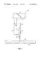
- FIG. 1is a schematic side view of a first preferred embodiment of a wafer saw in accordance with the present invention
- FIG. 2is a schematic front view of the wafer saw illustrated in FIG. 1;
- FIG. 3is a schematic front view of a second embodiment of a wafer saw in accordance with the present invention.
- FIG. 4is a schematic view of a first silicon semiconductor wafer having a conventional configuration to be diced with the wafer saw of the present invention
- FIG. 5is a schematic view of a second silicon semiconductor wafer having variously sized semiconductor devices therein to be diced with the wafer saw of the present invention
- FIG. 6is a schematic front view of a third embodiment of a wafer saw in accordance with the present invention.
- FIG. 7is a schematic view of a third silicon semiconductor wafer having variously sized semiconductor devices therein to be diced with the wafer saw of the present invention.
- FIG. 8is a top elevation of a portion of a semiconductor substrate bearing conductive traces connected by tie bars.
- FIG. 9is a top elevation of a portion of a semiconductor substrate bearing three different types of components formed thereon.
- an exemplary wafer saw 10is comprised of a base 12 to which extension arms 14 and 15 suspended by support 16 are attached.
- a wafer saw blade 18is attached to a spindle or hub 20 which is rotatably attached to the extension arm 15 .
- the blade 18may be secured to the hub 20 and extension arm 15 by a threaded nut 21 or other means of attachment known in the art.
- the wafer saw 10also includes a translatable wafer table 22 movably attached in both X and Y directions (as indicated by arrows in FIGS. 1 and 2) to the base 12 .
- blade 18may be translatable relative to the table 22 to achieve the same relative X-Y movement of the blade 18 to the table 22 .
- a silicon wafer 24 to be scribed or sawedmay be securely mounted to the table 22 .
- sawincludes scribing of a wafer, the resulting scribe line 26 not completely extending through the wafer substrate.
- waferincludes traditional full semiconductor wafers of silicon, gallium arsenide, or indium phosphide and other semiconductor materials, partial wafers, and other equivalent structures known in the art wherein a semiconductor material table or substrate is present.
- SOIsilicon-on-insulator
- SOSsapphire
- waferso-called silicon-on-insulator or “SOI” structures, wherein silicon is carried on a glass, ceramic or sapphire (“SOS”) base, or other such structures as known in the art, are encompassed by the term “wafer” as used herein.
- semiconductor substratemay be used to identify wafers and other structures to be singulated into smaller elements.
- the saw 10is capable of lateral multi-indexing of the table 22 or blade 18 or, in other words, translatable from side-to-side in FIG. 2 and into and out of the plane of the page in FIG. 1, various non-uniform distances. As noted before, such non-uniform distances may be mere multiples of a unit distance, or may comprise unrelated varying distances, as desired. Accordingly, a wafer 24 having variously sized integrated circuits or other devices or components therein may be sectioned or diced into its non-uniformly sized components by the multi-indexing wafer saw 10 . In addition, as previously alluded, the saw 10 may be used to create scribe lines or cuts that do not extend through the wafer 24 . The wafer 24 can then subsequently be diced by other methods known in the art or sawed completely through after the blade 18 has been lowered to traverse the wafer to its full depth or thickness.
- FIG. 3another illustrated embodiment of a wafer saw 30 is shown having two laterally-spaced blades 32 and 34 with their centers of rotation in substantial parallel alignment transverse to the planes of the blades.
- a conventional substantially circular silicon semiconductor wafer 40flat omitted
- the bladescan be spaced a distance D substantially equal to the distance between adjacent streets 44 defining the space between each integrated circuit 42 .
- the streets 44 of wafer 40are too closely spaced for side-by-side blades 32 and 34 to cut along adjacent streets, the blades 32 and 34 can be spaced a distance D substantially equal to the distance between two or more streets.
- a first pass of the blades 32 and 34could cut along streets 44 a and 44 c and a second pass along streets 44 b and 44 d .
- the bladescould then be indexed to cut the next series of streets and the process repeated for streets 44 e , 44 f , 44 g , and 44 h .
- the integrated circuits of a wafer 52have various sizes, such as integrated circuits 50 and 51 , as illustrated in FIG. 5, at least one blade 34 is laterally translatable relative to the other blade 32 to cut along the streets, such as street 56 , separating the variously sized integrated circuits 50 .
- the blade 34may be variously translatable by a stepper motor 36 having a lead screw 38 or by other devices known in the art, such as high precision gearing in combination with an electric motor or hydraulics or other suitable mechanical drive and control assemblies.
- the integrated circuitssuch as integrated circuits 50 and 51
- the integrated circuitsmay be diced by setting the blades 32 and 34 to simultaneously cut along streets 56 and 57 , indexing the blades, setting them to a wider lateral spread and cutting along streets 58 and 59 , indexing the blades while monitoring the same lateral spread or separation and cutting along streets 60 and 61 , and then narrowing the blade spacing and indexing the blades and cutting along streets 62 and 63 .
- the wafer 52could then be rotated 90° and the blade separation and indexing process repeated for streets 64 and 65 , streets 66 and 67 , and streets 68 and 69 .
- a wafer saw 70As illustrated in FIG. 6, a wafer saw 70 according to the present invention is shown having two blades 72 and 74 , one of which is independently raisable (as indicated by an arrow) relative to the other.
- the term “raisable”includes vertical translation either up or down. Such a configuration may be beneficial for situations where the distance between adjacent streets is less than the minimum lateral achievable distance between blades 72 and 74 , or only a single column of narrow dice is to be cut, such as at the edge of a wafer.
- the two blades 72 and 74can make a first pass along streets 82 and 83 .
- the elevation mechanism 76 for blade 72may comprise a stepper motor, a precision-geared hydraulic or electric mechanism, a pivotable arm which is electrically, hydraulically or pneumatically powered, or other means well known in the art.
- a wafer sawcould use a single blade to cut along streets that are too closely spaced for dual-blade cutting or in other suitable situations, and use both blades to cut along variously spaced streets where the lateral distance between adjacent streets is sufficient for both blades to be engaged.
- test inserts or chip carriersformed from a silicon (or other semiconductor) wafer and used to make temporary or permanent chip-to-wafer, chip-to-chip and chip-to-carrier interconnections and that are cut into individual or groups of inserts, as described in U.S. Pat. Nos. 5,326,428 and 4,937,653, may benefit from the multi-indexing method and apparatus described herein.
- a semiconductor substrate 100may have traces 102 formed thereon by electrodeposition techniques that require connection of a plurality of traces 102 through a tie bar 104 .
- a two-blade saw in accordance with the present inventionmay be employed to simultaneously scribe substrate 100 along parallel lines 106 and 108 flanging a street 110 in order to sever tie bars 104 of adjacent substrate segments 112 from their associated traces 102 . Following such severance, the two columns of adjacent substrate segments 112 (corresponding to what would be termed “dice” if integrated circuits were formed thereon) are completely severed along street 110 after the two-blade saw is indexed for alignment of one blade therewith, and the other blade raised out of contact with substrate 100 .
- substrate segments 112 for test or packaging purposesmay be fabricated more efficiently in the same manner as dice and in the same sizes and shapes.
- RFID modulesmay be more easily fabricated when all components of a module are formed on a single wafer and retrieved therefrom for placement on a carrier substrate providing mechanical support and electrical interconnection between components.
- a portion of a substrate 200is depicted with three adjacent columns of varying-width segments, the three widths of segments illustrating batteries 202 , chips 204 and antennas 206 of an RFID device.
- an RFID modulemay be assembled by a single pick-and-place apparatus at a single work station.
- complete modulesmay be assembled without transfer of partially-assembled modules from one station to the next to add components.
- this approachmay be employed to any module assembly wherein all of the components are capable of being fabricated on a single semiconductor substrate.
- the present inventionhas particular applicability to the fabrication of custom or non-standard IC's or other components, wherein a capability for rapid and easy die size and shape adjustment on a wafer-by-wafer basis is highly beneficial and cost-effective.
- a capability for rapid and easy die size and shape adjustment on a wafer-by-wafer basisis highly beneficial and cost-effective.
- Those skilled in the artwill also understand that various combinations of the preferred embodiments could be made without departing from the spirit of the invention. For example, it may be desirable to have at least one blade of the independently laterally translatable blade configuration be independently raisable relative to the other blade or blades, or a single blade may be both translatable and raisable relative to one or more other blades and to the target wafer.
Landscapes
- Engineering & Computer Science (AREA)
- Mechanical Engineering (AREA)
- Physics & Mathematics (AREA)
- Condensed Matter Physics & Semiconductors (AREA)
- General Physics & Mathematics (AREA)
- Manufacturing & Machinery (AREA)
- Computer Hardware Design (AREA)
- Microelectronics & Electronic Packaging (AREA)
- Power Engineering (AREA)
- Dicing (AREA)
Abstract
Description
Claims (7)
Priority Applications (19)
| Application Number | Priority Date | Filing Date | Title |
|---|---|---|---|
| US08/747,299US6250192B1 (en) | 1996-11-12 | 1996-11-12 | Method for sawing wafers employing multiple indexing techniques for multiple die dimensions |
| US09/069,561US6119675A (en) | 1996-11-12 | 1998-04-29 | Method for sawing wafers employing multiple indexing techniques for multiple die dimensions |
| US09/271,086US6006739A (en) | 1996-11-12 | 1999-03-17 | Method for sawing wafers employing multiple indexing techniques for multiple die dimensions |
| US09/270,539US6155247A (en) | 1996-11-12 | 1999-03-17 | Method for sawing wafers employing multiple indexing techniques for multiple die dimensions |
| US09/434,147US6196096B1 (en) | 1996-11-12 | 1999-11-04 | Method for sawing wafers employing multiple indexing techniques for multiple die dimensions |
| US09/567,643US6401580B1 (en) | 1996-11-12 | 2000-05-09 | Method for sawing wafers employing multiple indexing techniques for multiple die dimensions |
| US09/567,262US6255196B1 (en) | 1996-11-12 | 2000-05-09 | Method for sawing wafers employing multiple indexing techniques for multiple die dimensions |
| US09/602,403US6279563B1 (en) | 1996-11-12 | 2000-06-22 | Method for sawing wafers employing multiple indexing techniques for multiple die dimensions |
| US09/753,159US6427676B2 (en) | 1996-11-12 | 2001-01-02 | Method for sawing wafers employing multiple indexing techniques for multiple die dimensions |
| US09/862,943US6631662B2 (en) | 1996-11-12 | 2001-05-22 | Apparatus for sawing wafers employing multiple indexing techniques for multiple die dimensions |
| US09/864,737US6459105B2 (en) | 1996-11-12 | 2001-05-23 | Apparatus for sawing wafers employing multiple indexing techniques for multiple die dimensions |
| US09/864,911US6423616B2 (en) | 1996-11-12 | 2001-05-23 | Method for sawing wafers employing multiple indexing techniques for multiple die dimensions |
| US09/901,838US6493934B2 (en) | 1996-11-12 | 2001-07-10 | Method for sawing wafers employing multiple indexing techniques for multiple die dimensions |
| US09/978,480US6691696B2 (en) | 1996-11-12 | 2001-10-17 | Method for sawing wafers employing multiple indexing techniques for multiple die dimensions |
| US10/101,041US6578458B1 (en) | 1996-11-12 | 2002-03-18 | Method for sawing wafers employing multiple indexing techniques for multiple die dimensions |
| US10/223,923US6687990B2 (en) | 1996-11-12 | 2002-08-20 | Sawing method employing multiple indexing techniques and semiconductor device structures fabricated thereby |
| US10/263,319US6897571B2 (en) | 1996-11-12 | 2002-10-01 | Method for sawing wafers employing multiple indexing techniques for multiple die dimensions |
| US10/701,957US6932077B2 (en) | 1996-11-12 | 2003-11-05 | Method for sawing wafers employing multiple indexing techniques for multiple die dimensions and dicing apparatus |
| US11/137,048US7387119B2 (en) | 1996-11-12 | 2005-05-25 | Dicing saw with variable indexing capability |
Applications Claiming Priority (1)
| Application Number | Priority Date | Filing Date | Title |
|---|---|---|---|
| US08/747,299US6250192B1 (en) | 1996-11-12 | 1996-11-12 | Method for sawing wafers employing multiple indexing techniques for multiple die dimensions |
Related Child Applications (2)
| Application Number | Title | Priority Date | Filing Date |
|---|---|---|---|
| US09/069,561DivisionUS6119675A (en) | 1996-11-12 | 1998-04-29 | Method for sawing wafers employing multiple indexing techniques for multiple die dimensions |
| US09/862,943ContinuationUS6631662B2 (en) | 1996-11-12 | 2001-05-22 | Apparatus for sawing wafers employing multiple indexing techniques for multiple die dimensions |
Publications (1)
| Publication Number | Publication Date |
|---|---|
| US6250192B1true US6250192B1 (en) | 2001-06-26 |
Family
ID=25004503
Family Applications (16)
| Application Number | Title | Priority Date | Filing Date |
|---|---|---|---|
| US08/747,299Expired - LifetimeUS6250192B1 (en) | 1996-11-12 | 1996-11-12 | Method for sawing wafers employing multiple indexing techniques for multiple die dimensions |
| US09/069,561Expired - LifetimeUS6119675A (en) | 1996-11-12 | 1998-04-29 | Method for sawing wafers employing multiple indexing techniques for multiple die dimensions |
| US09/270,539Expired - LifetimeUS6155247A (en) | 1996-11-12 | 1999-03-17 | Method for sawing wafers employing multiple indexing techniques for multiple die dimensions |
| US09/434,147Expired - LifetimeUS6196096B1 (en) | 1996-11-12 | 1999-11-04 | Method for sawing wafers employing multiple indexing techniques for multiple die dimensions |
| US09/567,262Expired - Fee RelatedUS6255196B1 (en) | 1996-11-12 | 2000-05-09 | Method for sawing wafers employing multiple indexing techniques for multiple die dimensions |
| US09/567,643Expired - Fee RelatedUS6401580B1 (en) | 1996-11-12 | 2000-05-09 | Method for sawing wafers employing multiple indexing techniques for multiple die dimensions |
| US09/602,403Expired - LifetimeUS6279563B1 (en) | 1996-11-12 | 2000-06-22 | Method for sawing wafers employing multiple indexing techniques for multiple die dimensions |
| US09/753,159Expired - LifetimeUS6427676B2 (en) | 1996-11-12 | 2001-01-02 | Method for sawing wafers employing multiple indexing techniques for multiple die dimensions |
| US09/862,943Expired - Fee RelatedUS6631662B2 (en) | 1996-11-12 | 2001-05-22 | Apparatus for sawing wafers employing multiple indexing techniques for multiple die dimensions |
| US09/864,911Expired - Fee RelatedUS6423616B2 (en) | 1996-11-12 | 2001-05-23 | Method for sawing wafers employing multiple indexing techniques for multiple die dimensions |
| US09/864,737Expired - Fee RelatedUS6459105B2 (en) | 1996-11-12 | 2001-05-23 | Apparatus for sawing wafers employing multiple indexing techniques for multiple die dimensions |
| US09/978,480Expired - Fee RelatedUS6691696B2 (en) | 1996-11-12 | 2001-10-17 | Method for sawing wafers employing multiple indexing techniques for multiple die dimensions |
| US10/101,041Expired - Fee RelatedUS6578458B1 (en) | 1996-11-12 | 2002-03-18 | Method for sawing wafers employing multiple indexing techniques for multiple die dimensions |
| US10/263,319Expired - Fee RelatedUS6897571B2 (en) | 1996-11-12 | 2002-10-01 | Method for sawing wafers employing multiple indexing techniques for multiple die dimensions |
| US10/701,957Expired - Fee RelatedUS6932077B2 (en) | 1996-11-12 | 2003-11-05 | Method for sawing wafers employing multiple indexing techniques for multiple die dimensions and dicing apparatus |
| US11/137,048Expired - Fee RelatedUS7387119B2 (en) | 1996-11-12 | 2005-05-25 | Dicing saw with variable indexing capability |
Family Applications After (15)
| Application Number | Title | Priority Date | Filing Date |
|---|---|---|---|
| US09/069,561Expired - LifetimeUS6119675A (en) | 1996-11-12 | 1998-04-29 | Method for sawing wafers employing multiple indexing techniques for multiple die dimensions |
| US09/270,539Expired - LifetimeUS6155247A (en) | 1996-11-12 | 1999-03-17 | Method for sawing wafers employing multiple indexing techniques for multiple die dimensions |
| US09/434,147Expired - LifetimeUS6196096B1 (en) | 1996-11-12 | 1999-11-04 | Method for sawing wafers employing multiple indexing techniques for multiple die dimensions |
| US09/567,262Expired - Fee RelatedUS6255196B1 (en) | 1996-11-12 | 2000-05-09 | Method for sawing wafers employing multiple indexing techniques for multiple die dimensions |
| US09/567,643Expired - Fee RelatedUS6401580B1 (en) | 1996-11-12 | 2000-05-09 | Method for sawing wafers employing multiple indexing techniques for multiple die dimensions |
| US09/602,403Expired - LifetimeUS6279563B1 (en) | 1996-11-12 | 2000-06-22 | Method for sawing wafers employing multiple indexing techniques for multiple die dimensions |
| US09/753,159Expired - LifetimeUS6427676B2 (en) | 1996-11-12 | 2001-01-02 | Method for sawing wafers employing multiple indexing techniques for multiple die dimensions |
| US09/862,943Expired - Fee RelatedUS6631662B2 (en) | 1996-11-12 | 2001-05-22 | Apparatus for sawing wafers employing multiple indexing techniques for multiple die dimensions |
| US09/864,911Expired - Fee RelatedUS6423616B2 (en) | 1996-11-12 | 2001-05-23 | Method for sawing wafers employing multiple indexing techniques for multiple die dimensions |
| US09/864,737Expired - Fee RelatedUS6459105B2 (en) | 1996-11-12 | 2001-05-23 | Apparatus for sawing wafers employing multiple indexing techniques for multiple die dimensions |
| US09/978,480Expired - Fee RelatedUS6691696B2 (en) | 1996-11-12 | 2001-10-17 | Method for sawing wafers employing multiple indexing techniques for multiple die dimensions |
| US10/101,041Expired - Fee RelatedUS6578458B1 (en) | 1996-11-12 | 2002-03-18 | Method for sawing wafers employing multiple indexing techniques for multiple die dimensions |
| US10/263,319Expired - Fee RelatedUS6897571B2 (en) | 1996-11-12 | 2002-10-01 | Method for sawing wafers employing multiple indexing techniques for multiple die dimensions |
| US10/701,957Expired - Fee RelatedUS6932077B2 (en) | 1996-11-12 | 2003-11-05 | Method for sawing wafers employing multiple indexing techniques for multiple die dimensions and dicing apparatus |
| US11/137,048Expired - Fee RelatedUS7387119B2 (en) | 1996-11-12 | 2005-05-25 | Dicing saw with variable indexing capability |
Country Status (1)
| Country | Link |
|---|---|
| US (16) | US6250192B1 (en) |
Cited By (11)
| Publication number | Priority date | Publication date | Assignee | Title |
|---|---|---|---|---|
| US6423616B2 (en)* | 1996-11-12 | 2002-07-23 | Micron Technology, Inc. | Method for sawing wafers employing multiple indexing techniques for multiple die dimensions |
| US20020185121A1 (en)* | 2001-06-06 | 2002-12-12 | Farnworth Warren M. | Group encapsulated dicing chuck |
| US20030131707A1 (en)* | 2000-06-06 | 2003-07-17 | Mikio Yotsumoto | Cutting device and cutting method |
| US6606985B2 (en)* | 2001-02-07 | 2003-08-19 | Disco Corporation | Dual-cutting method devoid of useless strokes |
| US20030199165A1 (en)* | 2002-03-11 | 2003-10-23 | Becton, Dickinson And Company | System and method for the manufacture of surgical blades |
| US6687990B2 (en)* | 1996-11-12 | 2004-02-10 | Micron Technology, Inc. | Sawing method employing multiple indexing techniques and semiconductor device structures fabricated thereby |
| US20050037359A1 (en)* | 2002-10-29 | 2005-02-17 | Kiyoharu Oono | Process for producing labeled nucleic acids or proteins |
| US20100011925A1 (en)* | 2008-07-16 | 2010-01-21 | Sang-Hyung Lim | Mother substrate cutting apparatus, method of cutting a mother substrate using the same and organic light emitting diode display cut thereby |
| US20110061787A1 (en)* | 2009-09-14 | 2011-03-17 | Primera Technology, Inc. | System For Finishing Printed Labels Using Multiple X-Y Cutters |
| US9963962B2 (en) | 2001-11-19 | 2018-05-08 | Packers Plus Energy Services Inc. | Method and apparatus for wellbore fluid treatment |
| US11225943B2 (en)* | 2019-04-23 | 2022-01-18 | Best Blade Recycling, Llc | System and method for three dimensional positioning a wind turbine blade and a plurality of saw blades with respect to each other for making a plurality of cuts in a wind turbine blades for recycling |
Families Citing this family (103)
| Publication number | Priority date | Publication date | Assignee | Title |
|---|---|---|---|---|
| JP3203365B2 (en)* | 1997-12-02 | 2001-08-27 | 株式会社東京精密 | Work cutting method in dicing machine |
| KR100285413B1 (en)* | 1998-09-03 | 2001-04-02 | 김세광 | Rim type diamond blade |
| EP1242218B1 (en)* | 1999-01-22 | 2007-03-28 | Jesse G. Cogswell | Blade ring saw assembly |
| JP4347960B2 (en)* | 1999-09-14 | 2009-10-21 | 株式会社ディスコ | Dicing method |
| JP4640715B2 (en)* | 2000-07-14 | 2011-03-02 | 株式会社ディスコ | Alignment method and alignment apparatus |
| JP3834000B2 (en)* | 2000-10-05 | 2006-10-18 | 本田技研工業株式会社 | Metal sheet drum cutting device |
| US20020081772A1 (en)* | 2000-12-21 | 2002-06-27 | Madrid Ruben P. | Method and system for manufacturing ball grid array ("BGA") packages |
| DE10136534B4 (en) | 2001-07-26 | 2006-05-11 | Disco Hi-Tec Europe Gmbh | Wafer cutting machine |
| SG118084A1 (en)* | 2001-08-24 | 2006-01-27 | Micron Technology Inc | Method and apparatus for cutting semiconductor wafers |
| US6787382B1 (en) | 2001-08-30 | 2004-09-07 | Micron Technology, Inc. | Method and system for singulating semiconductor components |
| SG139508A1 (en)* | 2001-09-10 | 2008-02-29 | Micron Technology Inc | Wafer dicing device and method |
| SG102639A1 (en)* | 2001-10-08 | 2004-03-26 | Micron Technology Inc | Apparatus and method for packing circuits |
| JP2003151920A (en)* | 2001-11-09 | 2003-05-23 | Disco Abrasive Syst Ltd | Workpiece positioning method for cutting machine |
| US20030140496A1 (en)* | 2002-01-31 | 2003-07-31 | Shen Buswell | Methods and systems for forming slots in a semiconductor substrate |
| US7387742B2 (en)* | 2002-03-11 | 2008-06-17 | Becton, Dickinson And Company | Silicon blades for surgical and non-surgical use |
| US6639302B2 (en)* | 2002-03-20 | 2003-10-28 | International Business Machines Corporation | Stress reduction in flip-chip PBGA packaging by utilizing segmented chip carries |
| GB0212775D0 (en)* | 2002-05-31 | 2002-07-10 | Westwind Air Bearings Ltd | Machine apparatus and methods |
| SG142115A1 (en) | 2002-06-14 | 2008-05-28 | Micron Technology Inc | Wafer level packaging |
| CA2394560C (en)* | 2002-07-24 | 2007-05-29 | Linden Fabricating & Engineering (Prince George) Ltd. | Log merchandiser |
| US20040161871A1 (en)* | 2002-11-27 | 2004-08-19 | Seiko Epson Corporation | Semiconductor device, method of manufacturing the same, circuit substrate and electronic equipment |
| WO2004067214A2 (en)* | 2003-01-24 | 2004-08-12 | Cogswell Jesse G | Blade ring saw blade |
| US20050155955A1 (en)* | 2003-03-10 | 2005-07-21 | Daskal Vadim M. | Method for reducing glare and creating matte finish of controlled density on a silicon surface |
| US20090007436A1 (en)* | 2003-03-10 | 2009-01-08 | Daskal Vadim M | Silicon blades for surgical and non-surgical use |
| US20060278956A1 (en)* | 2003-03-13 | 2006-12-14 | Pdf Solutions, Inc. | Semiconductor wafer with non-rectangular shaped dice |
| SG119185A1 (en) | 2003-05-06 | 2006-02-28 | Micron Technology Inc | Method for packaging circuits and packaged circuits |
| JP2007514457A (en)* | 2003-09-17 | 2007-06-07 | ベクトン・ディキンソン・アンド・カンパニー | System and method for creating straight and non-linear grooves using routers in silicon and other crystalline materials |
| US7232957B2 (en)* | 2003-09-25 | 2007-06-19 | Sanyo Electric Co., Ltd. | Hybrid integrated circuit device and method of manufacturing the same |
| US7703365B2 (en)* | 2004-01-08 | 2010-04-27 | Usnr/Kockums Cancar Company | Laterally movable trim saw |
| DE102004014644A1 (en)* | 2004-03-25 | 2005-10-13 | Atmel Germany Gmbh | Integrated circuit |
| US7396484B2 (en)* | 2004-04-30 | 2008-07-08 | Becton, Dickinson And Company | Methods of fabricating complex blade geometries from silicon wafers and strengthening blade geometries |
| US7302751B2 (en)* | 2004-04-30 | 2007-12-04 | Hewlett-Packard Development Company, L.P. | Method of fabricating a rat's nest RFID antenna |
| US7181837B2 (en)* | 2004-06-04 | 2007-02-27 | Micron Technology, Inc. | Plating buss and a method of use thereof |
| EA201400189A1 (en) | 2004-06-29 | 2014-09-30 | Текстура Корпорейшн | SYSTEM AND METHOD OF PAYMENT MANAGEMENT IN CONSTRUCTION |
| CN100440444C (en)* | 2004-07-22 | 2008-12-03 | 株式会社瑞萨科技 | Method for manufacturing semiconductor device |
| JP2007036143A (en)* | 2005-07-29 | 2007-02-08 | Disco Abrasive Syst Ltd | Machining method of semiconductor wafer |
| US7563694B2 (en)* | 2006-12-01 | 2009-07-21 | Atmel Corporation | Scribe based bond pads for integrated circuits |
| KR100871709B1 (en)* | 2007-04-10 | 2008-12-08 | 삼성전자주식회사 | Chip stack package and manufacturing method thereof |
| US7798703B2 (en)* | 2007-05-09 | 2010-09-21 | Infineon Technologies Ag | Apparatus and method for measuring local surface temperature of semiconductor device |
| US20080295664A1 (en)* | 2007-06-01 | 2008-12-04 | Semion Stolyar | Web-slitter with electronic motor control |
| GB2451697A (en)* | 2007-08-10 | 2009-02-11 | Sigmala Ltd | Adjustable slitting knife holder |
| US7972940B2 (en)* | 2007-12-28 | 2011-07-05 | Micron Technology, Inc. | Wafer processing |
| US8591287B2 (en)* | 2010-02-26 | 2013-11-26 | Corning Incorporated | Methods of fabricating a honeycomb extrusion die from a die body |
| KR101064977B1 (en)* | 2011-05-04 | 2011-09-15 | (주)아이에스티 코리아 | Thin Light Guide Panel Processing Equipment Engraved with Engraved Dot Pattern |
| EP2706920A4 (en)* | 2011-05-13 | 2014-11-05 | Parace Llc | Medical examination apparatus |
| US8647966B2 (en)* | 2011-06-09 | 2014-02-11 | National Semiconductor Corporation | Method and apparatus for dicing die attach film on a semiconductor wafer |
| US20130273717A1 (en)* | 2012-04-17 | 2013-10-17 | Taiwan Semiconductor Manufacturing Co., Ltd. | Apparatus and Method for the Singulation of a Semiconductor Wafer |
| JP5871711B2 (en)* | 2012-05-21 | 2016-03-01 | ユニ・チャーム株式会社 | Web member cutting apparatus having a plurality of fibers including tows, and cutting method |
| JP5656915B2 (en)* | 2012-05-21 | 2015-01-21 | ユニ・チャーム株式会社 | Web member cutting apparatus having a plurality of fibers including tows, and cutting method |
| JP5836194B2 (en)* | 2012-05-21 | 2015-12-24 | ユニ・チャーム株式会社 | Cutting apparatus for continuous web having a plurality of fibers including tow, and cutting method |
| US9812350B2 (en) | 2013-03-06 | 2017-11-07 | Qorvo Us, Inc. | Method of manufacture for a silicon-on-plastic semiconductor device with interfacial adhesion layer |
| US9583414B2 (en) | 2013-10-31 | 2017-02-28 | Qorvo Us, Inc. | Silicon-on-plastic semiconductor device and method of making the same |
| US9252478B2 (en) | 2013-03-15 | 2016-02-02 | A.K. Stamping Company, Inc. | Method of manufacturing stamped antenna |
| US9409394B2 (en) | 2013-05-31 | 2016-08-09 | Stmicroelectronics, Inc. | Method of making inkjet print heads by filling residual slotted recesses and related devices |
| TWI582847B (en) | 2014-09-12 | 2017-05-11 | Rf微型儀器公司 | Printed circuit module having semiconductor device with a polymer substrate and methods of manufacturing the same |
| US10085352B2 (en) | 2014-10-01 | 2018-09-25 | Qorvo Us, Inc. | Method for manufacturing an integrated circuit package |
| US9530709B2 (en) | 2014-11-03 | 2016-12-27 | Qorvo Us, Inc. | Methods of manufacturing a printed circuit module having a semiconductor device with a protective layer in place of a low-resistivity handle layer |
| US9406347B2 (en) | 2014-12-18 | 2016-08-02 | Freescale Semiconductor, Inc. | Semiconductor wafer and method of fabricating an IC die |
| US9960145B2 (en) | 2015-03-25 | 2018-05-01 | Qorvo Us, Inc. | Flip chip module with enhanced properties |
| US9613831B2 (en) | 2015-03-25 | 2017-04-04 | Qorvo Us, Inc. | Encapsulated dies with enhanced thermal performance |
| US20160343604A1 (en) | 2015-05-22 | 2016-11-24 | Rf Micro Devices, Inc. | Substrate structure with embedded layer for post-processing silicon handle elimination |
| CN104827594A (en)* | 2015-06-11 | 2015-08-12 | 河南鸿昌电子有限公司 | Wire cutting machine capable of pouring bonding agent |
| US9592563B1 (en) | 2015-07-20 | 2017-03-14 | Harley D. James, Jr. | Two-bladed table saw with selective stationary blade |
| US10276495B2 (en) | 2015-09-11 | 2019-04-30 | Qorvo Us, Inc. | Backside semiconductor die trimming |
| CN105643818A (en)* | 2015-12-31 | 2016-06-08 | 湖南大学 | Multi-blade cutting device and cutting method |
| US10020405B2 (en) | 2016-01-19 | 2018-07-10 | Qorvo Us, Inc. | Microelectronics package with integrated sensors |
| EP3211666A1 (en)* | 2016-02-26 | 2017-08-30 | Infineon Technologies AG | Multiple substrate |
| US10062583B2 (en) | 2016-05-09 | 2018-08-28 | Qorvo Us, Inc. | Microelectronics package with inductive element and magnetically enhanced mold compound component |
| US10773952B2 (en) | 2016-05-20 | 2020-09-15 | Qorvo Us, Inc. | Wafer-level package with enhanced performance |
| US10784149B2 (en) | 2016-05-20 | 2020-09-22 | Qorvo Us, Inc. | Air-cavity module with enhanced device isolation |
| US10468329B2 (en) | 2016-07-18 | 2019-11-05 | Qorvo Us, Inc. | Thermally enhanced semiconductor package having field effect transistors with back-gate feature |
| US10103080B2 (en) | 2016-06-10 | 2018-10-16 | Qorvo Us, Inc. | Thermally enhanced semiconductor package with thermal additive and process for making the same |
| US10109550B2 (en) | 2016-08-12 | 2018-10-23 | Qorvo Us, Inc. | Wafer-level package with enhanced performance |
| SG11201901193UA (en) | 2016-08-12 | 2019-03-28 | Qorvo Us Inc | Wafer-level package with enhanced performance |
| US10486965B2 (en) | 2016-08-12 | 2019-11-26 | Qorvo Us, Inc. | Wafer-level package with enhanced performance |
| US10109502B2 (en) | 2016-09-12 | 2018-10-23 | Qorvo Us, Inc. | Semiconductor package with reduced parasitic coupling effects and process for making the same |
| US10090339B2 (en) | 2016-10-21 | 2018-10-02 | Qorvo Us, Inc. | Radio frequency (RF) switch |
| US10749518B2 (en) | 2016-11-18 | 2020-08-18 | Qorvo Us, Inc. | Stacked field-effect transistor switch |
| US10068831B2 (en) | 2016-12-09 | 2018-09-04 | Qorvo Us, Inc. | Thermally enhanced semiconductor package and process for making the same |
| IT201700019300A1 (en)* | 2017-02-21 | 2018-08-21 | Nuova Ceram Casa S P A | METHOD OF MANUFACTURING OF FRAMEWORK SHEETS IN CERAMIC MATERIAL |
| US10647017B2 (en) | 2017-05-26 | 2020-05-12 | Gemini Saw Company, Inc. | Fluid-driven ring saw |
| US10755992B2 (en) | 2017-07-06 | 2020-08-25 | Qorvo Us, Inc. | Wafer-level packaging for enhanced performance |
| US10366972B2 (en) | 2017-09-05 | 2019-07-30 | Qorvo Us, Inc. | Microelectronics package with self-aligned stacked-die assembly |
| US10784233B2 (en) | 2017-09-05 | 2020-09-22 | Qorvo Us, Inc. | Microelectronics package with self-aligned stacked-die assembly |
| US11152363B2 (en) | 2018-03-28 | 2021-10-19 | Qorvo Us, Inc. | Bulk CMOS devices with enhanced performance and methods of forming the same utilizing bulk CMOS process |
| US12062700B2 (en) | 2018-04-04 | 2024-08-13 | Qorvo Us, Inc. | Gallium-nitride-based module with enhanced electrical performance and process for making the same |
| US12046505B2 (en) | 2018-04-20 | 2024-07-23 | Qorvo Us, Inc. | RF devices with enhanced performance and methods of forming the same utilizing localized SOI formation |
| US10804246B2 (en) | 2018-06-11 | 2020-10-13 | Qorvo Us, Inc. | Microelectronics package with vertically stacked dies |
| CN118213279A (en) | 2018-07-02 | 2024-06-18 | Qorvo美国公司 | RF semiconductor device and method for manufacturing the same |
| US11069590B2 (en) | 2018-10-10 | 2021-07-20 | Qorvo Us, Inc. | Wafer-level fan-out package with enhanced performance |
| US10964554B2 (en) | 2018-10-10 | 2021-03-30 | Qorvo Us, Inc. | Wafer-level fan-out package with enhanced performance |
| US11646242B2 (en) | 2018-11-29 | 2023-05-09 | Qorvo Us, Inc. | Thermally enhanced semiconductor package with at least one heat extractor and process for making the same |
| US12046483B2 (en) | 2019-01-23 | 2024-07-23 | Qorvo Us, Inc. | RF devices with enhanced performance and methods of forming the same |
| US12046570B2 (en) | 2019-01-23 | 2024-07-23 | Qorvo Us, Inc. | RF devices with enhanced performance and methods of forming the same |
| US12057374B2 (en) | 2019-01-23 | 2024-08-06 | Qorvo Us, Inc. | RF devices with enhanced performance and methods of forming the same |
| KR20250027591A (en) | 2019-01-23 | 2025-02-26 | 코르보 유에스, 인크. | Rf semiconductor device and manufacturing method thereof |
| US12125825B2 (en) | 2019-01-23 | 2024-10-22 | Qorvo Us, Inc. | RF devices with enhanced performance and methods of forming the same |
| US11387157B2 (en) | 2019-01-23 | 2022-07-12 | Qorvo Us, Inc. | RF devices with enhanced performance and methods of forming the same |
| US12074086B2 (en) | 2019-11-01 | 2024-08-27 | Qorvo Us, Inc. | RF devices with nanotube particles for enhanced performance and methods of forming the same |
| CN110843150A (en)* | 2019-11-27 | 2020-02-28 | 湖南大合新材料有限公司 | Tellurium-zinc-cadmium polycrystal cutting device |
| US11646289B2 (en) | 2019-12-02 | 2023-05-09 | Qorvo Us, Inc. | RF devices with enhanced performance and methods of forming the same |
| US11923238B2 (en) | 2019-12-12 | 2024-03-05 | Qorvo Us, Inc. | Method of forming RF devices with enhanced performance including attaching a wafer to a support carrier by a bonding technique without any polymer adhesive |
| US12129168B2 (en) | 2019-12-23 | 2024-10-29 | Qorvo Us, Inc. | Microelectronics package with vertically stacked MEMS device and controller device |
| WO2022186857A1 (en) | 2021-03-05 | 2022-09-09 | Qorvo Us, Inc. | Selective etching process for si-ge and doped epitaxial silicon |
Citations (42)
| Publication number | Priority date | Publication date | Assignee | Title |
|---|---|---|---|---|
| DE287869C (en)* | ||||
| US2762954A (en) | 1950-09-09 | 1956-09-11 | Sylvania Electric Prod | Method for assembling transistors |
| US2865082A (en) | 1953-07-16 | 1958-12-23 | Sylvania Electric Prod | Semiconductor mount and method |
| US3664389A (en)* | 1970-06-01 | 1972-05-23 | Exil E Bower | Lateral adjustment means for radial arm saws |
| US3688815A (en)* | 1971-04-30 | 1972-09-05 | Charles A Ridenour | Radial arm saw depth gauge |
| US3691707A (en)* | 1969-11-12 | 1972-09-19 | Sola Basic Ind | Semiconductor material cutting apparatus and method of making the same |
| US3795164A (en)* | 1971-06-19 | 1974-03-05 | Gen Corrugated Machinery | Device for straight-line slitting and cutting of corrugated paper |
| US3892156A (en)* | 1974-02-11 | 1975-07-01 | Johnstone Eng & Mach Co | Knife holders for slitter winding machines and the like |
| US3961547A (en)* | 1974-11-20 | 1976-06-08 | Maurice Shainberg | Paper scoring and slitting machine |
| US4006656A (en)* | 1974-10-25 | 1977-02-08 | Kabushiki Kaisha Tomoku | Scoring and cutting apparatus for an elongated sheet |
| US4102227A (en)* | 1976-05-03 | 1978-07-25 | Ppg Industries, Inc. | Method of and apparatus for aligning a scoring wheel with a support wheel |
| US4138304A (en) | 1977-11-03 | 1979-02-06 | General Electric Company | Wafer sawing technique |
| US4259886A (en)* | 1979-06-20 | 1981-04-07 | Seid Bobby P | Wood cutter and loader |
| US4287256A (en) | 1978-12-26 | 1981-09-01 | Rca Corporation | Wafer and boule protection during the blade return stroke of a wafer saw |
| US4287798A (en)* | 1980-01-31 | 1981-09-08 | Cooper Jr Hill M | Sawmill work feeding and product handling apparatus |
| US4343662A (en) | 1981-03-31 | 1982-08-10 | Atlantic Richfield Company | Manufacturing semiconductor wafer devices by simultaneous slicing and etching |
| US4358978A (en)* | 1979-06-26 | 1982-11-16 | The Head Wrightson Machine Co. Ltd. | Trimming strip material |
| US4451972A (en) | 1980-01-21 | 1984-06-05 | National Semiconductor Corporation | Method of making electronic chip with metalized back including a surface stratum of solder |
| US4513544A (en)* | 1982-04-30 | 1985-04-30 | Wacker-Chemitronic Gesellschaft Fur Elektronik-Grundstoffe Mbh | Method of sawing crystalline rods, and multiple-blade internal-hole saw for carrying out the method |
| US4688540A (en) | 1984-12-27 | 1987-08-25 | Disco Abrasive Systems, Ltd. | Semiconductor wafer dicing machine |
| US4705016A (en) | 1985-05-17 | 1987-11-10 | Disco Abrasive Systems, Ltd. | Precision device for reducing errors attributed to temperature change reduced |
| US4804641A (en) | 1985-09-30 | 1989-02-14 | Siemens Aktiengesellschaft | Method for limiting chippage when sawing a semiconductor wafer |
| US4903437A (en) | 1987-07-31 | 1990-02-27 | Mitsubishi Kinzoku Kabushiki Kaisha | Slicing machine for cutting semiconductor material |
| US4937653A (en) | 1988-07-21 | 1990-06-26 | American Telephone And Telegraph Company | Semiconductor integrated circuit chip-to-chip interconnection scheme |
| US4971201A (en) | 1989-03-30 | 1990-11-20 | Sathre Robert C | Stacking rim for soft-sided containers |
| US5046392A (en)* | 1989-04-06 | 1991-09-10 | Richard Keon | Cutter for preparing an insulation batt for installation |
| US5059899A (en) | 1990-08-16 | 1991-10-22 | Micron Technology, Inc. | Semiconductor dies and wafers and methods for making |
| US5128282A (en) | 1991-11-04 | 1992-07-07 | Xerox Corporation | Process for separating image sensor dies and the like from a wafer that minimizes silicon waste |
| US5259149A (en) | 1991-12-18 | 1993-11-09 | St. Florian Company | Dicing blade hub and method |
| US5316559A (en) | 1991-12-18 | 1994-05-31 | St. Florian Company | Dicing blade composition |
| US5323150A (en) | 1992-06-11 | 1994-06-21 | Micron Technology, Inc. | Method for reducing conductive and convective heat loss from the battery in an RFID tag or other battery-powered devices |
| US5326428A (en) | 1993-09-03 | 1994-07-05 | Micron Semiconductor, Inc. | Method for testing semiconductor circuitry for operability and method of forming apparatus for testing semiconductor circuitry for operability |
| US5362681A (en) | 1992-07-22 | 1994-11-08 | Anaglog Devices, Inc. | Method for separating circuit dies from a wafer |
| US5373834A (en)* | 1992-04-03 | 1994-12-20 | Chiuminatta; Edward R. | Mounting arbor for saw cutting blades |
| US5458034A (en)* | 1992-12-30 | 1995-10-17 | Elio Cavagna S.R.L. | Apparatus for the transverse cutting of materials of various type, especially in the form of ribbons |
| US5461008A (en) | 1994-05-26 | 1995-10-24 | Delco Electronics Corporatinon | Method of preventing aluminum bond pad corrosion during dicing of integrated circuit wafers |
| US5468541A (en) | 1993-09-07 | 1995-11-21 | United Microelectronics Corporation | Thin film delamination test chip |
| US5521125A (en) | 1994-10-28 | 1996-05-28 | Xerox Corporation | Precision dicing of silicon chips from a wafer |
| US5580831A (en)* | 1993-07-28 | 1996-12-03 | Fujitsu Limited | Sawcut method of forming alignment marks on two faces of a substrate |
| US5579671A (en)* | 1995-01-18 | 1996-12-03 | Bowlin; William P. | Automatic stem cutting apparatus and method |
| US5851845A (en) | 1995-12-18 | 1998-12-22 | Micron Technology, Inc. | Process for packaging a semiconductor die using dicing and testing |
| US5907984A (en)* | 1995-04-19 | 1999-06-01 | Cutting Edge Inc. | Parallel cutting assembly for cutting sheet material |
Family Cites Families (60)
| Publication number | Priority date | Publication date | Assignee | Title |
|---|---|---|---|---|
| US2792954A (en)* | 1953-05-15 | 1957-05-21 | Vulcan Res Corp | Material handling device |
| GB1001908A (en)* | 1962-08-31 | 1965-08-18 | Texas Instruments Inc | Semiconductor devices |
| US3861547A (en)* | 1973-11-28 | 1975-01-21 | Sr Fred N Sink | Container transporting and maintaining apparatus |
| US4246595A (en)* | 1977-03-08 | 1981-01-20 | Matsushita Electric Industrial Co., Ltd. | Electronics circuit device and method of making the same |
| US4150912A (en) | 1978-01-23 | 1979-04-24 | Monsanto Company | Twin blade mounting and tensioning apparatus |
| US4343084A (en) | 1980-02-08 | 1982-08-10 | Rca Corporation | Method for making printed circuit boards with connector terminals |
| US4396140A (en)* | 1981-01-27 | 1983-08-02 | Bell Telephone Laboratories, Incorporated | Method of bonding electronic components |
| FR2527036A1 (en)* | 1982-05-14 | 1983-11-18 | Radiotechnique Compelec | METHOD FOR CONNECTING A SEMICONDUCTOR TO ELEMENTS OF A SUPPORT, PARTICULARLY A PORTABLE CARD |
| DE3235650A1 (en)* | 1982-09-27 | 1984-03-29 | Philips Patentverwaltung Gmbh, 2000 Hamburg | INFORMATION CARD AND METHOD FOR THEIR PRODUCTION |
| FR2581480A1 (en)* | 1985-04-10 | 1986-11-07 | Ebauches Electroniques Sa | ELECTRONIC UNIT, IN PARTICULAR FOR A MICROCIRCUIT BOARD AND CARD COMPRISING SUCH A UNIT |
| US4748495A (en)* | 1985-08-08 | 1988-05-31 | Dypax Systems Corporation | High density multi-chip interconnection and cooling package |
| US4648495A (en)* | 1985-08-28 | 1987-03-10 | J. I. Case Company | Clutch assembly and lubrication arrangement |
| GB8606045D0 (en)* | 1986-03-12 | 1986-04-16 | Emi Plc Thorn | Gas sensitive device |
| US5243208A (en)* | 1987-05-27 | 1993-09-07 | Hitachi, Ltd. | Semiconductor integrated circuit device having a gate array with a ram and by-pass signal lines which interconnect a logic section and I/O unit circuit of the gate array |
| US4971021A (en)* | 1987-07-31 | 1990-11-20 | Mitsubishi Kinzoku Kabushiki Kaisha | Apparatus for cutting semiconductor crystal |
| US5016138A (en)* | 1987-10-27 | 1991-05-14 | Woodman John K | Three dimensional integrated circuit package |
| US4992850A (en)* | 1989-02-15 | 1991-02-12 | Micron Technology, Inc. | Directly bonded simm module |
| US5016080A (en)* | 1988-10-07 | 1991-05-14 | Exar Corporation | Programmable die size continuous array |
| US4992849A (en)* | 1989-02-15 | 1991-02-12 | Micron Technology, Inc. | Directly bonded board multiple integrated circuit module |
| US5255156A (en)* | 1989-02-22 | 1993-10-19 | The Boeing Company | Bonding pad interconnection on a multiple chip module having minimum channel width |
| US4984358A (en) | 1989-03-10 | 1991-01-15 | Microelectronics And Computer Technology Corporation | Method of assembling stacks of integrated circuit dies |
| DE3911711A1 (en)* | 1989-04-10 | 1990-10-11 | Ibm | MODULE STRUCTURE WITH INTEGRATED SEMICONDUCTOR CHIP AND CHIP CARRIER |
| US4991000A (en)* | 1989-08-31 | 1991-02-05 | Bone Robert L | Vertically interconnected integrated circuit chip system |
| US5200362A (en)* | 1989-09-06 | 1993-04-06 | Motorola, Inc. | Method of attaching conductive traces to an encapsulated semiconductor die using a removable transfer film |
| US5459340A (en) | 1989-10-03 | 1995-10-17 | Trw Inc. | Adaptive configurable gate array |
| US5182632A (en)* | 1989-11-22 | 1993-01-26 | Tactical Fabs, Inc. | High density multichip package with interconnect structure and heatsink |
| US5045921A (en)* | 1989-12-26 | 1991-09-03 | Motorola, Inc. | Pad array carrier IC device using flexible tape |
| US5227338A (en)* | 1990-04-30 | 1993-07-13 | International Business Machines Corporation | Three-dimensional memory card structure with internal direct chip attachment |
| US5118369A (en)* | 1990-08-23 | 1992-06-02 | Colorcode Unlimited Corporation | Microlabelling system and process for making microlabels |
| US5064781A (en)* | 1990-08-31 | 1991-11-12 | Motorola, Inc. | Method of fabricating integrated silicon and non-silicon semiconductor devices |
| US5107328A (en)* | 1991-02-13 | 1992-04-21 | Micron Technology, Inc. | Packaging means for a semiconductor die having particular shelf structure |
| US5137836A (en)* | 1991-05-23 | 1992-08-11 | Atmel Corporation | Method of manufacturing a repairable multi-chip module |
| US5256578A (en)* | 1991-12-23 | 1993-10-26 | Motorola, Inc. | Integral semiconductor wafer map recording |
| JPH05169885A (en)* | 1991-12-26 | 1993-07-09 | Mitsubishi Electric Corp | Thin IC card |
| US5280193A (en)* | 1992-05-04 | 1994-01-18 | Lin Paul T | Repairable semiconductor multi-package module having individualized package bodies on a PC board substrate |
| US5422435A (en)* | 1992-05-22 | 1995-06-06 | National Semiconductor Corporation | Stacked multi-chip modules and method of manufacturing |
| US5787174A (en) | 1992-06-17 | 1998-07-28 | Micron Technology, Inc. | Remote identification of integrated circuit |
| US5319521A (en) | 1992-08-17 | 1994-06-07 | Rockwell International Corporation | Ceramic frames and capsules for Z-axis modules |
| US5438216A (en)* | 1992-08-31 | 1995-08-01 | Motorola, Inc. | Light erasable multichip module |
| GB2283863A (en) | 1993-11-16 | 1995-05-17 | Ibm | Direct chip attach module |
| US5477082A (en)* | 1994-01-11 | 1995-12-19 | Exponential Technology, Inc. | Bi-planar multi-chip module |
| US5418687A (en)* | 1994-02-01 | 1995-05-23 | Hewlett-Packard Company | Wafer scale multi-chip module |
| US5532457A (en)* | 1994-06-22 | 1996-07-02 | International Business Machines Corporation | Modified quartz plate to provide non-uniform light source |
| US6117707A (en) | 1994-07-13 | 2000-09-12 | Shellcase Ltd. | Methods of producing integrated circuit devices |
| JPH0837210A (en)* | 1994-07-22 | 1996-02-06 | Nec Kyushu Ltd | Method of preserving mapping data of semiconductor wafer |
| US5465470A (en)* | 1994-08-31 | 1995-11-14 | Lsi Logic Corporation | Fixture for attaching multiple lids to multi-chip module (MCM) integrated circuit |
| US5604673A (en)* | 1995-06-07 | 1997-02-18 | Hughes Electronics | Low temperature co-fired ceramic substrates for power converters |
| US5483503A (en)* | 1995-06-30 | 1996-01-09 | Durel Corporation | Split chip inverter for EL lamp |
| US5612513A (en)* | 1995-09-19 | 1997-03-18 | Micron Communications, Inc. | Article and method of manufacturing an enclosed electrical circuit using an encapsulant |
| EP0856198B1 (en) | 1995-10-16 | 2002-01-02 | Siemens N.V. | Polymer stud-matrix housing for microwave circuit arrangements |
| KR100192216B1 (en)* | 1996-02-29 | 1999-06-15 | 황인길 | Wafer Map Conversion Method |
| US5729438A (en)* | 1996-06-07 | 1998-03-17 | Motorola, Inc. | Discrete component pad array carrier |
| US6006739A (en)* | 1996-11-12 | 1999-12-28 | Micron Technology, Inc. | Method for sawing wafers employing multiple indexing techniques for multiple die dimensions |
| US6250192B1 (en)* | 1996-11-12 | 2001-06-26 | Micron Technology, Inc. | Method for sawing wafers employing multiple indexing techniques for multiple die dimensions |
| US6104333A (en) | 1996-12-19 | 2000-08-15 | Micron Technology, Inc. | Methods of processing wireless communication, methods of processing radio frequency communication, and related systems |
| FR2764111A1 (en) | 1997-06-03 | 1998-12-04 | Sgs Thomson Microelectronics | METHOD FOR MANUFACTURING SEMICONDUCTOR PACKAGES INCLUDING AN INTEGRATED CIRCUIT |
| US6268796B1 (en) | 1997-12-12 | 2001-07-31 | Alfred Gnadinger | Radio frequency identification transponder having integrated antenna |
| US6104291A (en) | 1998-01-09 | 2000-08-15 | Intermec Ip Corp. | Method and apparatus for testing RFID tags |
| US6156625A (en)* | 1998-03-07 | 2000-12-05 | Texas Instruments Incorporated | Partial semiconductor wafer processing using wafermap display |
| US6130473A (en)* | 1998-04-02 | 2000-10-10 | National Semiconductor Corporation | Lead frame chip scale package |
- 1996
- 1996-11-12USUS08/747,299patent/US6250192B1/ennot_activeExpired - Lifetime
- 1998
- 1998-04-29USUS09/069,561patent/US6119675A/ennot_activeExpired - Lifetime
- 1999
- 1999-03-17USUS09/270,539patent/US6155247A/ennot_activeExpired - Lifetime
- 1999-11-04USUS09/434,147patent/US6196096B1/ennot_activeExpired - Lifetime
- 2000
- 2000-05-09USUS09/567,262patent/US6255196B1/ennot_activeExpired - Fee Related
- 2000-05-09USUS09/567,643patent/US6401580B1/ennot_activeExpired - Fee Related
- 2000-06-22USUS09/602,403patent/US6279563B1/ennot_activeExpired - Lifetime
- 2001
- 2001-01-02USUS09/753,159patent/US6427676B2/ennot_activeExpired - Lifetime
- 2001-05-22USUS09/862,943patent/US6631662B2/ennot_activeExpired - Fee Related
- 2001-05-23USUS09/864,911patent/US6423616B2/ennot_activeExpired - Fee Related
- 2001-05-23USUS09/864,737patent/US6459105B2/ennot_activeExpired - Fee Related
- 2001-10-17USUS09/978,480patent/US6691696B2/ennot_activeExpired - Fee Related
- 2002
- 2002-03-18USUS10/101,041patent/US6578458B1/ennot_activeExpired - Fee Related
- 2002-10-01USUS10/263,319patent/US6897571B2/ennot_activeExpired - Fee Related
- 2003
- 2003-11-05USUS10/701,957patent/US6932077B2/ennot_activeExpired - Fee Related
- 2005
- 2005-05-25USUS11/137,048patent/US7387119B2/ennot_activeExpired - Fee Related
Patent Citations (43)
| Publication number | Priority date | Publication date | Assignee | Title |
|---|---|---|---|---|
| DE287869C (en)* | ||||
| US2762954A (en) | 1950-09-09 | 1956-09-11 | Sylvania Electric Prod | Method for assembling transistors |
| US2865082A (en) | 1953-07-16 | 1958-12-23 | Sylvania Electric Prod | Semiconductor mount and method |
| US3691707A (en)* | 1969-11-12 | 1972-09-19 | Sola Basic Ind | Semiconductor material cutting apparatus and method of making the same |
| US3664389A (en)* | 1970-06-01 | 1972-05-23 | Exil E Bower | Lateral adjustment means for radial arm saws |
| US3688815A (en)* | 1971-04-30 | 1972-09-05 | Charles A Ridenour | Radial arm saw depth gauge |
| US3795164A (en)* | 1971-06-19 | 1974-03-05 | Gen Corrugated Machinery | Device for straight-line slitting and cutting of corrugated paper |
| US3892156A (en)* | 1974-02-11 | 1975-07-01 | Johnstone Eng & Mach Co | Knife holders for slitter winding machines and the like |
| US4006656A (en)* | 1974-10-25 | 1977-02-08 | Kabushiki Kaisha Tomoku | Scoring and cutting apparatus for an elongated sheet |
| US3961547A (en)* | 1974-11-20 | 1976-06-08 | Maurice Shainberg | Paper scoring and slitting machine |
| US4102227A (en)* | 1976-05-03 | 1978-07-25 | Ppg Industries, Inc. | Method of and apparatus for aligning a scoring wheel with a support wheel |
| US4138304A (en) | 1977-11-03 | 1979-02-06 | General Electric Company | Wafer sawing technique |
| US4287256A (en) | 1978-12-26 | 1981-09-01 | Rca Corporation | Wafer and boule protection during the blade return stroke of a wafer saw |
| US4259886A (en)* | 1979-06-20 | 1981-04-07 | Seid Bobby P | Wood cutter and loader |
| US4358978A (en)* | 1979-06-26 | 1982-11-16 | The Head Wrightson Machine Co. Ltd. | Trimming strip material |
| US4451972A (en) | 1980-01-21 | 1984-06-05 | National Semiconductor Corporation | Method of making electronic chip with metalized back including a surface stratum of solder |
| US4287798A (en)* | 1980-01-31 | 1981-09-08 | Cooper Jr Hill M | Sawmill work feeding and product handling apparatus |
| US4343662A (en) | 1981-03-31 | 1982-08-10 | Atlantic Richfield Company | Manufacturing semiconductor wafer devices by simultaneous slicing and etching |
| US4513544A (en)* | 1982-04-30 | 1985-04-30 | Wacker-Chemitronic Gesellschaft Fur Elektronik-Grundstoffe Mbh | Method of sawing crystalline rods, and multiple-blade internal-hole saw for carrying out the method |
| US4633847A (en) | 1982-04-30 | 1987-01-06 | Wacker-Chemie Gesellschaft Fur Elektronik-Grundstoffe Mbh | Multiple-blade internal-hole saw for sawing crystalline rods |
| US4688540A (en) | 1984-12-27 | 1987-08-25 | Disco Abrasive Systems, Ltd. | Semiconductor wafer dicing machine |
| US4705016A (en) | 1985-05-17 | 1987-11-10 | Disco Abrasive Systems, Ltd. | Precision device for reducing errors attributed to temperature change reduced |
| US4804641A (en) | 1985-09-30 | 1989-02-14 | Siemens Aktiengesellschaft | Method for limiting chippage when sawing a semiconductor wafer |
| US4903437A (en) | 1987-07-31 | 1990-02-27 | Mitsubishi Kinzoku Kabushiki Kaisha | Slicing machine for cutting semiconductor material |
| US4937653A (en) | 1988-07-21 | 1990-06-26 | American Telephone And Telegraph Company | Semiconductor integrated circuit chip-to-chip interconnection scheme |
| US4971201A (en) | 1989-03-30 | 1990-11-20 | Sathre Robert C | Stacking rim for soft-sided containers |
| US5046392A (en)* | 1989-04-06 | 1991-09-10 | Richard Keon | Cutter for preparing an insulation batt for installation |
| US5059899A (en) | 1990-08-16 | 1991-10-22 | Micron Technology, Inc. | Semiconductor dies and wafers and methods for making |
| US5128282A (en) | 1991-11-04 | 1992-07-07 | Xerox Corporation | Process for separating image sensor dies and the like from a wafer that minimizes silicon waste |
| US5259149A (en) | 1991-12-18 | 1993-11-09 | St. Florian Company | Dicing blade hub and method |
| US5316559A (en) | 1991-12-18 | 1994-05-31 | St. Florian Company | Dicing blade composition |
| US5373834A (en)* | 1992-04-03 | 1994-12-20 | Chiuminatta; Edward R. | Mounting arbor for saw cutting blades |
| US5323150A (en) | 1992-06-11 | 1994-06-21 | Micron Technology, Inc. | Method for reducing conductive and convective heat loss from the battery in an RFID tag or other battery-powered devices |
| US5362681A (en) | 1992-07-22 | 1994-11-08 | Anaglog Devices, Inc. | Method for separating circuit dies from a wafer |
| US5458034A (en)* | 1992-12-30 | 1995-10-17 | Elio Cavagna S.R.L. | Apparatus for the transverse cutting of materials of various type, especially in the form of ribbons |
| US5580831A (en)* | 1993-07-28 | 1996-12-03 | Fujitsu Limited | Sawcut method of forming alignment marks on two faces of a substrate |
| US5326428A (en) | 1993-09-03 | 1994-07-05 | Micron Semiconductor, Inc. | Method for testing semiconductor circuitry for operability and method of forming apparatus for testing semiconductor circuitry for operability |
| US5468541A (en) | 1993-09-07 | 1995-11-21 | United Microelectronics Corporation | Thin film delamination test chip |
| US5461008A (en) | 1994-05-26 | 1995-10-24 | Delco Electronics Corporatinon | Method of preventing aluminum bond pad corrosion during dicing of integrated circuit wafers |
| US5521125A (en) | 1994-10-28 | 1996-05-28 | Xerox Corporation | Precision dicing of silicon chips from a wafer |
| US5579671A (en)* | 1995-01-18 | 1996-12-03 | Bowlin; William P. | Automatic stem cutting apparatus and method |
| US5907984A (en)* | 1995-04-19 | 1999-06-01 | Cutting Edge Inc. | Parallel cutting assembly for cutting sheet material |
| US5851845A (en) | 1995-12-18 | 1998-12-22 | Micron Technology, Inc. | Process for packaging a semiconductor die using dicing and testing |
Cited By (29)
| Publication number | Priority date | Publication date | Assignee | Title |
|---|---|---|---|---|
| US6897571B2 (en) | 1996-11-12 | 2005-05-24 | Micron Technology, Inc. | Method for sawing wafers employing multiple indexing techniques for multiple die dimensions |
| US6427676B2 (en)* | 1996-11-12 | 2002-08-06 | Micron Technology, Inc. | Method for sawing wafers employing multiple indexing techniques for multiple die dimensions |
| US7387119B2 (en) | 1996-11-12 | 2008-06-17 | Micron Technology, Inc. | Dicing saw with variable indexing capability |
| US20030030122A1 (en)* | 1996-11-12 | 2003-02-13 | Salman Akram | Method for sawing wafers employing multiple indexing techniques for multiple die dimensions |
| US6578458B1 (en)* | 1996-11-12 | 2003-06-17 | Micron Technology, Inc. | Method for sawing wafers employing multiple indexing techniques for multiple die dimensions |
| US6631662B2 (en) | 1996-11-12 | 2003-10-14 | Micron Technology, Inc. | Apparatus for sawing wafers employing multiple indexing techniques for multiple die dimensions |
| US6423616B2 (en)* | 1996-11-12 | 2002-07-23 | Micron Technology, Inc. | Method for sawing wafers employing multiple indexing techniques for multiple die dimensions |
| US6687990B2 (en)* | 1996-11-12 | 2004-02-10 | Micron Technology, Inc. | Sawing method employing multiple indexing techniques and semiconductor device structures fabricated thereby |
| US6932077B2 (en) | 1996-11-12 | 2005-08-23 | Micron Technology, Inc. | Method for sawing wafers employing multiple indexing techniques for multiple die dimensions and dicing apparatus |
| US20030131707A1 (en)* | 2000-06-06 | 2003-07-17 | Mikio Yotsumoto | Cutting device and cutting method |
| US6606985B2 (en)* | 2001-02-07 | 2003-08-19 | Disco Corporation | Dual-cutting method devoid of useless strokes |
| US20050186761A1 (en)* | 2001-06-06 | 2005-08-25 | Farnworth Warren M. | Group encapsulated dicing chuck |
| US20070068504A1 (en)* | 2001-06-06 | 2007-03-29 | Farnworth Warren M | Group encapsulated dicing chuck |
| US20040031476A1 (en)* | 2001-06-06 | 2004-02-19 | Farnworth Warren M. | Group encapsulated dicing chuck |
| US20020185121A1 (en)* | 2001-06-06 | 2002-12-12 | Farnworth Warren M. | Group encapsulated dicing chuck |
| US20070062511A1 (en)* | 2001-06-06 | 2007-03-22 | Farnworth Warren M | Group encapsulated dicing chuck |
| US9963962B2 (en) | 2001-11-19 | 2018-05-08 | Packers Plus Energy Services Inc. | Method and apparatus for wellbore fluid treatment |
| US7906437B2 (en) | 2002-03-11 | 2011-03-15 | Beaver-Visitec International (Us), Inc. | System and method for the manufacture of surgical blades |
| US7105103B2 (en)* | 2002-03-11 | 2006-09-12 | Becton, Dickinson And Company | System and method for the manufacture of surgical blades |
| US20110192819A1 (en)* | 2002-03-11 | 2011-08-11 | Beaver-Vistec International, Inc. | System and method for the manufacture of surgical blades |
| US8409462B2 (en) | 2002-03-11 | 2013-04-02 | Beaver-Visitec International (Us), Inc. | System and method for the manufacture of surgical blades |
| US20030199165A1 (en)* | 2002-03-11 | 2003-10-23 | Becton, Dickinson And Company | System and method for the manufacture of surgical blades |
| US20050037359A1 (en)* | 2002-10-29 | 2005-02-17 | Kiyoharu Oono | Process for producing labeled nucleic acids or proteins |
| US20100011925A1 (en)* | 2008-07-16 | 2010-01-21 | Sang-Hyung Lim | Mother substrate cutting apparatus, method of cutting a mother substrate using the same and organic light emitting diode display cut thereby |
| US20130042735A1 (en)* | 2008-07-16 | 2013-02-21 | Sang-Hyung Lim | METHOD OF CUTTING A MOTHER SUBSTRATE [as amended] |
| US20110061787A1 (en)* | 2009-09-14 | 2011-03-17 | Primera Technology, Inc. | System For Finishing Printed Labels Using Multiple X-Y Cutters |
| US8663410B2 (en) | 2009-09-14 | 2014-03-04 | Primera Technology, Inc. | System for finishing printed labels using multiple X-Y cutters |
| US9199388B2 (en) | 2009-09-14 | 2015-12-01 | Primera Technology, Inc. | System for finishing printed labels using multiple X-Y cutters |
| US11225943B2 (en)* | 2019-04-23 | 2022-01-18 | Best Blade Recycling, Llc | System and method for three dimensional positioning a wind turbine blade and a plurality of saw blades with respect to each other for making a plurality of cuts in a wind turbine blades for recycling |
Also Published As
| Publication number | Publication date |
|---|---|
| US6459105B2 (en) | 2002-10-01 |
| US20040089282A1 (en) | 2004-05-13 |
| US6255196B1 (en) | 2001-07-03 |
| US20010023113A1 (en) | 2001-09-20 |
| US6423616B2 (en) | 2002-07-23 |
| US20010020408A1 (en) | 2001-09-13 |
| US6119675A (en) | 2000-09-19 |
| US20030030122A1 (en) | 2003-02-13 |
| US6897571B2 (en) | 2005-05-24 |
| US20010007254A1 (en) | 2001-07-12 |
| US20010023973A1 (en) | 2001-09-27 |
| US6155247A (en) | 2000-12-05 |
| US6427676B2 (en) | 2002-08-06 |
| US20020017177A1 (en) | 2002-02-14 |
| US6691696B2 (en) | 2004-02-17 |
| US6932077B2 (en) | 2005-08-23 |
| US6578458B1 (en) | 2003-06-17 |
| US7387119B2 (en) | 2008-06-17 |
| US6279563B1 (en) | 2001-08-28 |
| US20050211236A1 (en) | 2005-09-29 |
| US6401580B1 (en) | 2002-06-11 |
| US6196096B1 (en) | 2001-03-06 |
| US6631662B2 (en) | 2003-10-14 |
Similar Documents
| Publication | Publication Date | Title |
|---|---|---|
| US6250192B1 (en) | Method for sawing wafers employing multiple indexing techniques for multiple die dimensions | |
| US6006739A (en) | Method for sawing wafers employing multiple indexing techniques for multiple die dimensions | |
| US20070068504A1 (en) | Group encapsulated dicing chuck | |
| US6493934B2 (en) | Method for sawing wafers employing multiple indexing techniques for multiple die dimensions | |
| US7582513B2 (en) | Electronic device and method for producing electronic devices | |
| KR20130117324A (en) | Apparatus and method for the singulation of a semiconductor wafer | |
| US20060169680A1 (en) | Integrated, integrated circuit singulation system | |
| US6683378B2 (en) | System for singulating semiconductor components utilizing alignment pins | |
| US10692766B2 (en) | Method of cutting workpiece | |
| KR20110057454A (en) | Dual working table for dicing and dicing device including the same | |
| CN219636901U (en) | Semiconductor wafer | |
| CN113634875A (en) | Laser optical system and method for cutting semiconductor wafer | |
| JP2000031096A (en) | Method for cutting substrate | |
| GB2382218A (en) | Method for sawing a moulded leadframe package | |
| KR20080004790A (en) | Wafer sawing device |
Legal Events
| Date | Code | Title | Description |
|---|---|---|---|
| AS | Assignment | Owner name:MICRON TECHNOLOGY, INC., IDAHO Free format text:ASSIGNMENT OF ASSIGNORS INTEREST;ASSIGNORS:AKRAM, SALMAN;GOCHNOUR, DEREK J.;HESS, MICHAEL E.;AND OTHERS;REEL/FRAME:008312/0568 Effective date:19961106 | |
| FEPP | Fee payment procedure | Free format text:PAYOR NUMBER ASSIGNED (ORIGINAL EVENT CODE: ASPN); ENTITY STATUS OF PATENT OWNER: LARGE ENTITY | |
| STCF | Information on status: patent grant | Free format text:PATENTED CASE | |
| CC | Certificate of correction | ||
| FPAY | Fee payment | Year of fee payment:4 | |
| FPAY | Fee payment | Year of fee payment:8 | |
| FPAY | Fee payment | Year of fee payment:12 | |
| AS | Assignment | Owner name:U.S. BANK NATIONAL ASSOCIATION, AS COLLATERAL AGENT, CALIFORNIA Free format text:SECURITY INTEREST;ASSIGNOR:MICRON TECHNOLOGY, INC.;REEL/FRAME:038669/0001 Effective date:20160426 Owner name:U.S. BANK NATIONAL ASSOCIATION, AS COLLATERAL AGEN Free format text:SECURITY INTEREST;ASSIGNOR:MICRON TECHNOLOGY, INC.;REEL/FRAME:038669/0001 Effective date:20160426 | |
| AS | Assignment | Owner name:MORGAN STANLEY SENIOR FUNDING, INC., AS COLLATERAL AGENT, MARYLAND Free format text:PATENT SECURITY AGREEMENT;ASSIGNOR:MICRON TECHNOLOGY, INC.;REEL/FRAME:038954/0001 Effective date:20160426 Owner name:MORGAN STANLEY SENIOR FUNDING, INC., AS COLLATERAL Free format text:PATENT SECURITY AGREEMENT;ASSIGNOR:MICRON TECHNOLOGY, INC.;REEL/FRAME:038954/0001 Effective date:20160426 | |
| AS | Assignment | Owner name:U.S. BANK NATIONAL ASSOCIATION, AS COLLATERAL AGENT, CALIFORNIA Free format text:CORRECTIVE ASSIGNMENT TO CORRECT THE REPLACE ERRONEOUSLY FILED PATENT #7358718 WITH THE CORRECT PATENT #7358178 PREVIOUSLY RECORDED ON REEL 038669 FRAME 0001. ASSIGNOR(S) HEREBY CONFIRMS THE SECURITY INTEREST;ASSIGNOR:MICRON TECHNOLOGY, INC.;REEL/FRAME:043079/0001 Effective date:20160426 Owner name:U.S. BANK NATIONAL ASSOCIATION, AS COLLATERAL AGEN Free format text:CORRECTIVE ASSIGNMENT TO CORRECT THE REPLACE ERRONEOUSLY FILED PATENT #7358718 WITH THE CORRECT PATENT #7358178 PREVIOUSLY RECORDED ON REEL 038669 FRAME 0001. ASSIGNOR(S) HEREBY CONFIRMS THE SECURITY INTEREST;ASSIGNOR:MICRON TECHNOLOGY, INC.;REEL/FRAME:043079/0001 Effective date:20160426 | |
| AS | Assignment | Owner name:MICRON TECHNOLOGY, INC., IDAHO Free format text:RELEASE BY SECURED PARTY;ASSIGNOR:U.S. BANK NATIONAL ASSOCIATION, AS COLLATERAL AGENT;REEL/FRAME:047243/0001 Effective date:20180629 | |
| AS | Assignment | Owner name:MICRON TECHNOLOGY, INC., IDAHO Free format text:RELEASE BY SECURED PARTY;ASSIGNOR:MORGAN STANLEY SENIOR FUNDING, INC., AS COLLATERAL AGENT;REEL/FRAME:050937/0001 Effective date:20190731 |