US6249180B1 - Phase noise and additive noise estimation in a QAM demodulator - Google Patents
Phase noise and additive noise estimation in a QAM demodulatorDownload PDFInfo
- Publication number
- US6249180B1 US6249180B1US09/550,885US55088500AUS6249180B1US 6249180 B1US6249180 B1US 6249180B1US 55088500 AUS55088500 AUS 55088500AUS 6249180 B1US6249180 B1US 6249180B1
- Authority
- US
- United States
- Prior art keywords
- signal
- circuit
- qam
- demodulator
- coordinates
- Prior art date
- Legal status (The legal status is an assumption and is not a legal conclusion. Google has not performed a legal analysis and makes no representation as to the accuracy of the status listed.)
- Expired - Lifetime
Links
Images


Classifications
- H—ELECTRICITY
- H04—ELECTRIC COMMUNICATION TECHNIQUE
- H04L—TRANSMISSION OF DIGITAL INFORMATION, e.g. TELEGRAPHIC COMMUNICATION
- H04L27/00—Modulated-carrier systems
- H04L27/32—Carrier systems characterised by combinations of two or more of the types covered by groups H04L27/02, H04L27/10, H04L27/18 or H04L27/26
- H04L27/34—Amplitude- and phase-modulated carrier systems, e.g. quadrature-amplitude modulated carrier systems
- H04L27/38—Demodulator circuits; Receiver circuits
- H04L27/3809—Amplitude regulation arrangements
- H—ELECTRICITY
- H04—ELECTRIC COMMUNICATION TECHNIQUE
- H04L—TRANSMISSION OF DIGITAL INFORMATION, e.g. TELEGRAPHIC COMMUNICATION
- H04L27/00—Modulated-carrier systems
- H04L27/32—Carrier systems characterised by combinations of two or more of the types covered by groups H04L27/02, H04L27/10, H04L27/18 or H04L27/26
- H04L27/34—Amplitude- and phase-modulated carrier systems, e.g. quadrature-amplitude modulated carrier systems
- H04L27/38—Demodulator circuits; Receiver circuits
- H—ELECTRICITY
- H04—ELECTRIC COMMUNICATION TECHNIQUE
- H04L—TRANSMISSION OF DIGITAL INFORMATION, e.g. TELEGRAPHIC COMMUNICATION
- H04L1/00—Arrangements for detecting or preventing errors in the information received
- H04L1/004—Arrangements for detecting or preventing errors in the information received by using forward error control
- H04L1/0056—Systems characterized by the type of code used
- H04L1/0057—Block codes
- H—ELECTRICITY
- H04—ELECTRIC COMMUNICATION TECHNIQUE
- H04L—TRANSMISSION OF DIGITAL INFORMATION, e.g. TELEGRAPHIC COMMUNICATION
- H04L1/00—Arrangements for detecting or preventing errors in the information received
- H04L1/004—Arrangements for detecting or preventing errors in the information received by using forward error control
- H04L1/0056—Systems characterized by the type of code used
- H04L1/0071—Use of interleaving
- H—ELECTRICITY
- H04—ELECTRIC COMMUNICATION TECHNIQUE
- H04L—TRANSMISSION OF DIGITAL INFORMATION, e.g. TELEGRAPHIC COMMUNICATION
- H04L27/00—Modulated-carrier systems
- H04L27/32—Carrier systems characterised by combinations of two or more of the types covered by groups H04L27/02, H04L27/10, H04L27/18 or H04L27/26
- H04L27/34—Amplitude- and phase-modulated carrier systems, e.g. quadrature-amplitude modulated carrier systems
- H04L27/38—Demodulator circuits; Receiver circuits
- H04L27/3818—Demodulator circuits; Receiver circuits using coherent demodulation, i.e. using one or more nominally phase synchronous carriers
- H04L27/3827—Demodulator circuits; Receiver circuits using coherent demodulation, i.e. using one or more nominally phase synchronous carriers in which the carrier is recovered using only the demodulated baseband signals
- H—ELECTRICITY
- H04—ELECTRIC COMMUNICATION TECHNIQUE
- H04L—TRANSMISSION OF DIGITAL INFORMATION, e.g. TELEGRAPHIC COMMUNICATION
- H04L27/00—Modulated-carrier systems
- H04L27/32—Carrier systems characterised by combinations of two or more of the types covered by groups H04L27/02, H04L27/10, H04L27/18 or H04L27/26
- H04L27/34—Amplitude- and phase-modulated carrier systems, e.g. quadrature-amplitude modulated carrier systems
- H04L27/38—Demodulator circuits; Receiver circuits
- H04L27/3845—Demodulator circuits; Receiver circuits using non - coherent demodulation, i.e. not using a phase synchronous carrier
- H04L27/3854—Demodulator circuits; Receiver circuits using non - coherent demodulation, i.e. not using a phase synchronous carrier using a non - coherent carrier, including systems with baseband correction for phase or frequency offset
- H04L27/3872—Compensation for phase rotation in the demodulated signal
- H—ELECTRICITY
- H04—ELECTRIC COMMUNICATION TECHNIQUE
- H04L—TRANSMISSION OF DIGITAL INFORMATION, e.g. TELEGRAPHIC COMMUNICATION
- H04L27/00—Modulated-carrier systems
- H04L27/0014—Carrier regulation
- H04L2027/0024—Carrier regulation at the receiver end
- H04L2027/0026—Correction of carrier offset
- H04L2027/0032—Correction of carrier offset at baseband and passband
- H—ELECTRICITY
- H04—ELECTRIC COMMUNICATION TECHNIQUE
- H04L—TRANSMISSION OF DIGITAL INFORMATION, e.g. TELEGRAPHIC COMMUNICATION
- H04L27/00—Modulated-carrier systems
- H04L27/0014—Carrier regulation
- H04L2027/0024—Carrier regulation at the receiver end
- H04L2027/0026—Correction of carrier offset
- H04L2027/0036—Correction of carrier offset using a recovered symbol clock
- H—ELECTRICITY
- H04—ELECTRIC COMMUNICATION TECHNIQUE
- H04L—TRANSMISSION OF DIGITAL INFORMATION, e.g. TELEGRAPHIC COMMUNICATION
- H04L27/00—Modulated-carrier systems
- H04L27/0014—Carrier regulation
- H04L2027/0024—Carrier regulation at the receiver end
- H04L2027/0026—Correction of carrier offset
- H04L2027/0038—Correction of carrier offset using an equaliser
- H—ELECTRICITY
- H04—ELECTRIC COMMUNICATION TECHNIQUE
- H04L—TRANSMISSION OF DIGITAL INFORMATION, e.g. TELEGRAPHIC COMMUNICATION
- H04L27/00—Modulated-carrier systems
- H04L27/0014—Carrier regulation
- H04L2027/0044—Control loops for carrier regulation
- H04L2027/0053—Closed loops
- H04L2027/0055—Closed loops single phase
- H—ELECTRICITY
- H04—ELECTRIC COMMUNICATION TECHNIQUE
- H04L—TRANSMISSION OF DIGITAL INFORMATION, e.g. TELEGRAPHIC COMMUNICATION
- H04L27/00—Modulated-carrier systems
- H04L27/0014—Carrier regulation
- H04L2027/0044—Control loops for carrier regulation
- H04L2027/0053—Closed loops
- H04L2027/0057—Closed loops quadrature phase
- H—ELECTRICITY
- H04—ELECTRIC COMMUNICATION TECHNIQUE
- H04L—TRANSMISSION OF DIGITAL INFORMATION, e.g. TELEGRAPHIC COMMUNICATION
- H04L27/00—Modulated-carrier systems
- H04L27/0014—Carrier regulation
- H04L2027/0044—Control loops for carrier regulation
- H04L2027/0071—Control of loops
- H—ELECTRICITY
- H04—ELECTRIC COMMUNICATION TECHNIQUE
- H04L—TRANSMISSION OF DIGITAL INFORMATION, e.g. TELEGRAPHIC COMMUNICATION
- H04L27/00—Modulated-carrier systems
- H04L27/0014—Carrier regulation
- H04L2027/0044—Control loops for carrier regulation
- H04L2027/0071—Control of loops
- H04L2027/0079—Switching between loops
- H04L2027/0081—Switching between loops between loops of different bandwidths
- H—ELECTRICITY
- H04—ELECTRIC COMMUNICATION TECHNIQUE
- H04L—TRANSMISSION OF DIGITAL INFORMATION, e.g. TELEGRAPHIC COMMUNICATION
- H04L7/00—Arrangements for synchronising receiver with transmitter
- H04L7/0016—Arrangements for synchronising receiver with transmitter correction of synchronization errors
- H04L7/002—Arrangements for synchronising receiver with transmitter correction of synchronization errors correction by interpolation
- H04L7/0029—Arrangements for synchronising receiver with transmitter correction of synchronization errors correction by interpolation interpolation of received data signal
Definitions
- the present inventionrelates to a quadrature amplitude modulation (QAM) type demodulator for demodulating signals modulated in accordance with the QAM scheme.
- QAMquadrature amplitude modulation
- Quadrature amplitude modulationis an intermediate frequency (IF) modulation scheme in which a QAM signal is produced by amplitude modulating two baseband signals, generated independently of each other, with two quadrature carriers, respectively, and adding the resulting signals.
- the QAM modulationis used to modulate a digital information into a convenient frequency band. This may be to match the spectral band occupied by a signal to the passband of a transmission line, to allow frequency division multiplexing of signals, or to enable signals to be radiated by smaller antennas.
- QAMhas been adopted by the Digital Video Broadcasting (DVB) and Digital Audio Visual Council (DAVIC) and the Multimedia Cable Network System (MCNS) standardization bodies for the transmission of digital TV signals over Coaxial, Hybrid Fiber Coaxial (HFC), and Microwave Multi-port Distribution Wireless Systems (MMDS) TV networks.
- DVDDigital Video Broadcasting
- DAVICDigital Audio Visual Council
- MCNSMultimedia Cable Network System
- the QAM modulation schemeexists with a variable number of levels ( 4 , 16 , 32 , 64 , 128 , 256 , 512 , 1024 ) which provide 2, 4, 5, 6, 7, 8, 9, and 10 Mbit/s/MHz. This offers up to about 42 Mbit/s (QAM-256) over an American 6 MHz CATV channel, and 56 Mbit/s over an 8 MHz European CATV channel. This represents the equivalent of 10 PAL or SECAM TV channels transmitted over the equivalent bandwidth of a single analog TV program, and approximately 2 to 3 High Definition Television (HDTV) programs. Audio and video streams are digitally encoded and mapped into MPEG2 transport stream packets, consisting of 188 bytes.
- the bit streamis decomposed into n bits packets.
- the I and Q componentsare filtered and modulated using a sine and a cosine wave (carrier) leading to a unique Radio Frequency (RF) spectrum.
- the I and Q componentsare usually represented as a constellation which represents the possible discrete values taken over in-phase and quadrature coordinates.
- the transmitted signal s(t)is given by:
- f 0is the center frequency of the RF signal.
- I and Q componentsare usually filtered waveforms using raised cosine filtering at the transmitter and the receiver.
- the resulting RF spectrumis centered around f 0 and has a bandwidth of R(1+ ⁇ ), where R is the symbol transmission rate and ⁇ is the roll-off factor of the raised cosine filter.
- the symbol transmission rateis 1/n th of the transmission bit rate, since n bits are mapped to one QAM symbol per time unit 1/R.
- a demodulatorIn order to recover the baseband signals from the modulated carrier, a demodulator is used at the receiving end of the transmission line.
- the receivermust control the gain of the input amplifier that receives the signal, recover the symbol frequency of the signal, and recover the carrier frequency of the RF signal. After these main functions, a point is received in the I/Q constellation which is the sum of the transmitted QAM symbol and noise that was added over the transmission.
- the receiverthen carries out ⁇ threshold decision based on lines situated at half the distance between QAM symbols in order to decide on the most probable sent QAM symbol. From this symbol, the bits are unmapped using the same mapping as in the modulator.
- the bitsthen go through a forward error decoder which corrects possible erroneous decisions on the actual transmitted QAM symbol.
- the forward error decoderusually contains a de-interleaver whose role is to spread out errors that could have happened in bursts and would have otherwise have been more difficult to correct.
- phase noiseis generated by the various mixers and local oscillators in the modulator and the demodulator.
- the sidebands of the phase noise signalare coherent, which means that the upper frequency sidebands have a definite phase relationship to the lower frequency sidebands.
- Additive noisealso referred to as additive gaussian white noise, is random noise that has a frequency spectrum that is continuous and uniform over a specified frequency band. It is often very difficult to evaluate the amount of phase noise or additive noise for which the demodulator should compensate.
- the carrier loop bandwidthIn order to compensate for phase noise, the carrier loop bandwidth has to be increased. However, this causes the signal degradation caused by the additive noise to increase. In order to compensate for the additive noise, the carrier loop bandwidth should be decreased, but this causes the effect of increasing the phase noise degradation of the signal.
- a circuit in a synchronous detector systemthat is provided to minimize and compensate for the errors induced by phase modulation and additive noise in the system.
- a first-order correction of such errorsis achieved by equipping the synchronous detector system with a phase lock loop having a constant loop filter noise bandwidth to reduce the phase noise and an RMS detector for first order correction of the additive noise.
- the resolution filter passing the signal to the RMS detectoris made to have a noise bandwidth identical to the loop noise bandwidth.
- U.S. Pat. Nos. RE 31,351 and 4,213,095 to Falconerdiscloses, respectively, a feedback nonlinear equalization of modulated data signals and a feedforward nonlinear equalization of modulated data signals.
- a receiver for a QAM signal impaired by linear and non-linear distortion, phase jitter and additive noiseincludes circuitry which compensates for these impairments.
- the receiverincludes a processor which subtracts a feedback nonlinear signal from each sample of the received signal, either prior to or subsequent to demodulation, providing compensation for non-linear intersymbol interference.
- a feedforward non-linear signalis added to each sample of a linearly equalized received signal to provide compensation for nonlinear intersymbol interference.
- the feedback/feedforward nonlinear signalis comprises of a weighted sum of products of individual ones of the samples and their complex conjugates.
- the above objecthas been achieved by a QAM demodulator having a carrier recovery circuit that includes a phase estimation circuit and an additive noise estimation circuit which produces an estimation of the residual phase noise and additive noise viewed by the QAM demodulator.
- the inventionmakes it possible to estimate the required information in the field in order to optimize the carrier loop bandwidth and to reach the best bit error rate possible. This information can be used to select the carrier loop bandwidth that provides the best trade off between phase noise and additive noise.
- the phase noise estimationis based on the least mean square error between the QAM symbol decided by a symbol decision circuit and the received QAM symbol. The error is based only on QAM symbols having the maximum amplitude on I and Q coordinates.
- the additive noise estimationis based on the same error as in the phase noise estimation, except that it is based only on QAM symbols having the minimum amplitude on the I and Q coordinates.
- the additive noise estimatoris not dependent on the phase of the signal.
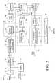
- FIG. 1is a block diagram of a Network Interface Unit in which the demodulator of the present invention may be used.
- FIG. 2is a block diagram of the demodulator of the present invention
- FIG. 3is a block diagram of the first AGC unit of th e demodulator shown in FIG. 2 .
- FIG. 4is a block diagram of the second AGC unit of t he demodulator shown in FIG. 2 .
- FIG. 5is a block diagram of a section of the demodulator shown in FIG. 2 .
- FIG. 6is a block diagram of the Direct Digital Synthesizer of the demodulator shown in FIG. 2 .
- FIG. 7is a block diagram of the digital timing recovery circuit of the demodulator shown in FIG. 2 .
- FIG. 8is a block diagram of a generally known interpolation model.
- FIG. 9is a block diagram of a n interpolation model used in the digital timing recovery circuit of FIG. 7 .
- FIG. 10is a block diagram of a phase noise and additive noise estimator used in the symbol detection circuit of the demodulator of FIG. 2 .
- FIG. 11is a block diagram of the Dual Bit Error Rate estimator used in the demodulator of FIG. 2 .
- the QAM demodulator 99 of the present inventionwould typically be used as part of a Network Interface Unit 92 .
- the Network Interface Unit 92is defined as the interface block between a signal 95 received from a Cable Network and the input signal 93 of a demultiplexer.
- the signal 95 from the cable networkis input into a tuner 96 .
- the tuneraccepts frequencies in the range of 47 MHz to 862 MHz at its input and down converts the selected frequency to an intermediate frequency (IF).
- IFintermediate frequency
- This IF frequencydepends on the channel bandwidth as related to the geographic location. For example, NTSC, USA and JAPAN have a 6 MHz channel with IF around 44 MHz, while PAL/SECAM and EUROPE have an 8 MHz channel with IF around 36 MHz.
- the output of the tuneris input to a surface acoustic wave (SAW) filter 97 , the IF frequency being equal to the SAW filter center frequency.
- SAWsurface acoustic wave
- the output of the SAW filter 97is supplied to an amplifier 98 , which is used to compensate for the SAW filter attenuation, and then the output of the amplifier 98 is supplied to the QAM demodulator 99 .
- the amplifier 98can also have a variable gain controlled by an Automatic Gain Control signal 94 of the QAM demodulator 99 . It is also possible for the QAM demodulator 99 to be used in various other digital transmission systems using QAM or QPSK demodulation, such as radio links, wireless local loops, or in-home networks.
- the QAM demodulator 99 of the present inventionincludes an analog-to-digital (A/D) converter 25 which receives the IF input signal 12 .
- the A/D converter 25samples the IF signal 12 and produces a digital spectrum around the center frequency F 0 , of the IF signal 12 .
- the output signal 14 of the A/D converter 25is supplied to a baseband conversion circuit that includes a Direct Digital Synthesizer 30 in order to convert the IF signal to a baseband signal.
- the output signal 14 of the A/D converter 25is also supplied to the first Automatic Gain Control circuit (AGC1) 10 for controlling the analog gain of the input signal 12 of the A/D converter 25 .
- AGC1Automatic Gain Control circuit
- the baseband signalis supplied to a timing recovery circuit 35 which is used to synchronize the timing of the demodulator circuit to the symbols of the incoming signals.
- the timing recovery circuit 35uses a continuously variable interpolation filter for sampling the input signal which allows the circuit to recover a very large range of symbol rates, as will be further explained below.
- the signalis then supplied to a digital multiplier 210 which is part of a second Automatic Gain Control (AGC2) circuit 20 . Then, the signal goes through a Receive Filter 40 and then to an Equalizer 45 .
- AGC2 circuit 20is a digital AGC circuit and performs a fine adjustment of the signal level at the equalizer 45 input.
- the digital AGC circuit 20only takes into account the signal itself, since adjacent channels have been filtered out by the receive filter 40 , and thus compensates digitally for the analog AGC1 circuit 10 which may have reduced the input power due to adjacent channels.
- the receive filter 40is a squared root raised cosine type which supports roll-off factors from 0.11 to 0.30, which accepts the timing recovery circuit output signal and ensures an out-of-band rejection higher than 43 dB. This significant rejection increases the back off margin of the Network Interface Unit against adjacent channels.
- the equalizer 45compensates for different impairments encountered on the network, such as undesired amplitude-frequency or phase-frequency response. Two equalizer structures can be selected, Transversal or Decision feedback with selectable central tap position.
- the output signals of the equalizer 45are supplied to the carrier recovery circuit 50 to recover the carrier signal.
- the carrier recovery circuit 50allows the acquisition and tracking of a frequency offset as high as 12 percent of the symbol rate.
- the frequency offset recoveredcan be monitored through a I2C interface. This information can be used to readjust the tuner or the demodulator frequency in order to reduce the filtering degradation of the signal, which helps to improve the bit error rate.
- the output signal 52 of the carrier recovery circuit 50is supplied to a symbol decision circuit 55 and is also supplied to a Power Comparator Circuit 230 and Digital Loop Filter 220 within the digital AGC2 circuit 20 to provide a gain control signal 225 to the multiplier 210 .
- the signalis supplied to a symbol threshold detector, then to a differential decoder, and finally to a DVB or DAVIC de-mapper which produces the recovered bit stream 57 sent to the Forward Error Correction Circuit 60 .
- the output 57 of the symbol decision circuitis also supplied to the Power Comparator Circuit 230 .
- the Forward Error Correction (FEC) circuit 60first performs a frame synchronization 61 in which the bit stream is decomposed into packets of 204 bytes at the output.
- the packetsare then supplied to a de-interleaver and Reed-Solomon (RS) decoder 65 , where the packets are de-interleaved and then a correction is performed by the RS decoder of a maximum of 8 errors (bytes) per packet.
- the RS decoderalso provides other information regarding the uncorrected packets and the position of the corrected bytes in the packet, if there are any. Two depths can be selected for the interleaver: 12 (DVB/DAVIC) and 17 .
- the depth 17increases the strength of the system against impulse noise, but assumes that the signal has been interleaved with the same value at the monitor.
- the packetsare de-scrambled for energy dispersal removal.
- the data output 93 of the FEC circuit 60is constituted of the MPEG2 Transport System (TS) packets and is the output of the demodulator 99 .
- bit error rate signals 68 , 69are transmitted to a Dual Bit Error Rate Estimator circuit 70 which estimate Low and High Bit Error Rates based on error correction and frame pattern recognition and produces a Bit Error Rate Signal 72 .
- the dual automatic gain control (AGC) circuitsare situated before and after the receive filters to control the received level of the signal.
- the first AGC circuit 10controls the analog gain of the input signal of the A/D converter.
- the output signal 14 of the A/D converter 25is supplied to a power estimation circuit 110 of the AGC1 10 in order to estimate the signal level of the received signal 14 and compare it to a predetermined signal level.
- the power estimation circuit 110includes a square module 130 for converting the signal 14 into a square wave to be input into a comparator 140 .
- the comparator 140compares the input signal with a predetermined reference voltage, or comparator threshold voltage, and produces an output signal when the level of the input signal matches the level of the comparator threshold voltage.
- the comparator threshold voltage, or reference voltagecan be adapted by a modification circuit 120 .
- the modification circuit 120monitors the presence of signals from adjacent channels 125 and adapts the reference voltage accordingly. Additionally, a detection of saturation counter 115 detects whether there is any saturation in the A/D converter and, if so, sends a signal to the modification circuit 120 in order to adjust the reference voltage in order to eliminate the saturation.
- the output signal of the power estimator circuit 110is supplied to a digital loop filter 150 which removes the carrier-frequency components and harmonics from the signal, but passes the original modulating frequencies of the signal.
- the digital loop filter 150receives a configuration signal 152 which sets the amplifier maximum gain configuration for limiting non-linearities.
- the output signal 162 of the digital loop filter 150is converted to a Pulse Width Modulated (PWM) signal 160 which is supplied to an RC filter 170 which produces a signal 167 that controls the analog gain of the amplifier of the A/D converter.
- PWMPulse Width Modulated
- Another output of the digital loop filterprovides a signal 155 for monitoring the gain value of the digital loop filter. Since the power estimation is estimated by the digital loop control, the PWM signal that controls the analog gain generates very stable control.
- the second AGC circuit 20is situated after the receive filter 40 , therefore only having to take into account the received power of the QAM signal itself, and adapts the internal amplification level to the correct level before threshold decision.
- the second AGC circuit 20compensates for the attenuation of the first AGC circuit 10 , which is caused by the presence of adjacent channels, and also adapts the signal level exactly to the decision threshold levels of the QAM signal.
- the output signal 42 of the timing recovery circuitis supplied to the digital multiplier 210 of the second AGC circuit 20 .
- the digital multiplier 210multiplies the signal, which is then supplied to the receive filter 40 , equalizer 45 and carrier recovery 50 circuits as explained above.
- the output of the carrier recovery circuit 50is fed back into a power comparator circuit 230 of the second AGC circuit 20 which compares the output signal 52 from the carrier recovery circuit with a set of QAM values.
- a digital loop filter 220filters out any error signals and provides a gain control signal 225 to the digital multiplier 210 . Additionally, a signal 227 can be provided from the digital loop filter in order to monitor the amount of gain.
- the aforementioned Direct Digital Synthesizer (DDS) 30digitally tunes the signal 14 from the A/D converter 25 to be within the bandwidth of the receive filter 40 even in the case of a large frequency offset of the receiver and provides more flexibility in the frequency values used by the input signal.
- the Intermediate Frequency (IF) to baseband signal conversionis accomplished by using a combination of a first DDS 30 before the receive filter 40 in order to digitally tune the signal within the receive filter bandwidth, and a second DDS 545 within the carrier recovery circuit 50 to fine tune the signal phase after the timing recovery 35 and equalizer 45 circuits.
- the output digital signal 14 of the A/D converteris supplied to a multiplier 304 that is part of DDS1 30 .
- the multiplier 304converts the digital signal 14 into two parallel components, I (inphase) and Q (quadrature) which form a QAM symbol. These signal components proceed through the receive filter 40 , equalizer 45 and carrier recovery 50 circuits, as explained above.
- the carrier recovery circuit 50includes a frequency offset detect 525 circuit and a phase offset detect 535 circuit for recovering the carrier signals to be sent to the digital AGC2 circuit 20 and the symbol detection circuit 55 .
- the frequency offset recoveredcan be monitored through an I 2 C interface and the information can be used to readjust the tuner frequency in order to reduce the filtering degradation on the signal and thus improve the bit error rate.
- This informationcan also be sent as a signal 527 to the DDS1 circuit 30 in order to recover the frequency with complete accuracy before the receive filter 40 .
- the phase detect circuit 535sends a signal 537 to the DDS2 circuit 545 .
- Employing a dual DDS structure to control the down conversion of the IF signal to a baseband signalis advantageous in that the long loop frequency down-conversion is optimal for frequency recovery since it is done before the receive filter 40 in order to maintain the maximum signal energy before equalization and carrier frequency estimation, while the short loop carrier phase recovery is optimal for phase tracking, especially in case of phase noise on the signal.
- the carrier recovery frequency feedback signal 527is supplied to an adder circuit 306 within the DDS1 circuit 30 .
- the adder circuit 306adds the frequency feedback signal 527 to the configured IF frequency 27 and the resulting signal is supplied to a phase accumulation circuit 305 which accumulates frequency elements determined by the frequency feedback signal 527 .
- the signalis supplied to a constant table 303 containing sinusoidal values which synthesizes the signal.
- the synthesized signal 316is supplied back into the multiplier 304 .
- the second DDS2 circuit 545operates in the same manner except that it synthesizes the output signal 537 of the phase detect circuit 535 .
- the purely digital carrier recoveryeliminates the need for a voltage controlled oscillator (VCO) to be used and provides a better carrier recovery in terms of accuracy and the residual phase noise of the signal.
- VCOvoltage controlled oscillator
- the timing recovery circuit 35uses a symbol rate continuously adaptive interpolation filter 352 for resampling the input signal.
- the method of interpolation used in the timing recovery circuit 35is defined as a function of t/T i (time/Interpolation Interval). This allows the interpolation filtering to be totally independent of the symbol rate in terms of performance and complexity and provides a better rejection of adjacent channels since the interpolator rejects most of the signal outside the bandwidth of the received channel.
- the objective of interpolation in modem applicationsis to process digital samples x(kT s ) 325 produced by an analog to digital converter at rate 1/T s , in order to generate “interpolants” y(kT i ) 365 at rate 1/T i , with 1/T i , multiple of the transmission baud rate 1/T.
- the numerically controlled oscillator 358produces two signals at each time mT s .
- the second signal 362is a Ti-fractional signal ⁇ , such that ⁇ T i represents the time since the last resample instant.
- the numerically controlled oscillator 358is controlled by a signal W(m) which estimates the ratio T s /T i .
- W(m)is delivered by a loop filter 356 driven by a phase error estimator or timing error detector 354 .
- ⁇ (m)1 if ⁇ (m ⁇ 1) ⁇ W(m) ⁇ 0
- the latest formulashows that the interpolants are computed by summing and delaying (I 1 +I 2 +1) terms a j (lT i ), where a j (lt i ) is the accumulation over the time interval [l ⁇ 1)T i , lT i ] of the multiplication of input samples x(mT s ) by coefficients h[(j+ ⁇ (m))T i ].
- a coefficient h[(j+ ⁇ (m))T i ]is delivered by a coefficient-computation block 909 with an input ⁇ (m) being output by the numerically controlled oscillator (NCO) 910 .
- the multiplier-accumulatorsoperate at frequency 1/T s and that the sum of aj is computed at frequency 1/T i .
- T s /T iFor a low ratio T s /T i , a high number of multiplication-accumulations are processed during a long T i period. This allows the T i —interpolator to have a longer time impulse response in regards to T s , and a narrower frequency bandwidth in regards to sampling frequency.
- Polynomials of degree 3have been chosen for a practical implementation because this is of reduced computation complexity and allows very good performances for the impulse response h(t), with only a few intervals T i (typically 4 to 8).
- a particular form of the polynomialscan also be used to further reduce the computational complexity. Once the degree, form and number (I 1 +I 2 +1) of polynomials is chosen, the parameters of the polynomials are computed by minimizing a cost function that represents the spectral constraints on the impulse response h(t).
- variable ⁇used for computing the coefficient h[(j+ ⁇ (m))T i ]
- T sinterpolation methods
- the previously described carrier recovery circuit 50includes a phase noise estimation circuit 506 and an additive noise estimation circuit 507 which produces an estimation of the residual phase noise and additive noise viewed by the QAM demodulator. This estimation allows the user to optimize the carrier loop bandwidth in order to reach the best trade off between the phase noise and the additive noise.
- the received QAM symbol 504is supplied to a symbol detection or decision block 508 .
- the received QAM symbol 504is a point in I/Q coordinates which is close in terms of distance to a possible transmitted QAM symbol, but is different because of noise.
- the symbol detection block 508decides on the most probable transmitted QAM symbol, by searching for the minimum distance between the received QAM symbol and possible transmitted QAM symbols (threshold symbols).
- the symbol detection block 508determines which QAM symbol was transmitted.
- the Least Mean Square (LMS) error between the decided QAM symbol 509 and the received QAM symbol 504is determined by the LMS error method 505 as known in the art and the LMS error signal 512 is supplied with the decided QAM symbol 509 to each of the phase noise 506 and additive noise 507 estimators.
- LMSLeast Mean Square
- the phase noise estimator result 518does not depend on the additive noise.
- the additive noise estimationis based on the same error signal 512 as in the phase noise estimation, but the error in the case of noise estimation is based only on QAM symbols having the minimum amplitude (
- 1) on I and Q.
- the additive noise estimator resultdoes not depend on the phase of the signal.
- the recovered bit stream 57 from the aforementioned symbol detection circuitis supplied to a Frame Synchronization Recovery (FSR) circuit 61 within the Forward Error Correction (FEC) decoder 60 .
- the FSR circuit 61decomposes the bit stream into packets of 204 bytes at the output. Then, the packets are supplied to a Frame Pattern Counter 62 which maintains a count of recognizable patterns of the frame over a sufficiently large number of frames in order to obtain additional information, such as synchronization patterns, that is not encoded by the FEC encoder. This information is input into a first Bit Error Rate Estimator 715 of the Dual BER unit 70 .
- the bit stream packetsthen are supplied to the de-interleaver and FEC decoder unit 65 which produces the MPEG TS data output signal 93 in the manner described above.
- the correctable errors 69are supplied to a counter 705 within the Dual BER unit 70 and then to a second Bit Error Rate estimator 716 .
- the outputs of the first BER estimator unit 715 and the second BER estimator unit 716go to a software processing unit 710 which compares the two BER outputs. This gives additional information about the type of noise, such as whether caused by a burst or by a distribution error. For low bit error rates, such as less than 10 ⁇ 3 , the second bit error rate estimator 716 will produce the more accurate value. For high BER, or in the case of burst errors, the second BER estimator 716 is not precise since the correction capacity of the code is exceeded. In this case, the first BER estimator 715 would be more precise.
- the Dual Bit Error Rate Estimator circuitallows it to be possible to evaluate the quality of a transmission link even in case of a severely distorted or noisy channel, which can help to identify the cause of bad reception.
- the FEC decoder 65gives a very accurate information when the interleaver strength provides sufficient error spreading to distribute errors uniformly over the frame and below the correction capability of the error correcting code, but very inaccurate information in case of long burst errors.
- a comparison between the two types of informationprovides a way to detect the kind of noise errors which may occur on the network. This allows, for instance, detection of whether a bad reception is due to burst noise or other problems such as phase noise, fading, etc.
- the FEC decodermay show a relatively low bit error rate although all of the errors may have occurred at a particular instant of transmission, which may have completely altered the information content carried by the transmission link, e.g. TV pictures, audio sound, etc.
- the Dual BER Estimator circuitmakes it easier to determine the cause of the poor transmission and thus solve the problem.
Landscapes
- Engineering & Computer Science (AREA)
- Computer Networks & Wireless Communication (AREA)
- Signal Processing (AREA)
- Digital Transmission Methods That Use Modulated Carrier Waves (AREA)
Abstract
Description


Claims (15)
Priority Applications (13)
| Application Number | Priority Date | Filing Date | Title |
|---|---|---|---|
| US09/550,885US6249180B1 (en) | 1999-09-08 | 2000-04-17 | Phase noise and additive noise estimation in a QAM demodulator |
| EP01909286AEP1201066B1 (en) | 2000-04-17 | 2001-02-15 | Phase noise and additive noise estimation in a qam carrier recovery circuit |
| AU2001237059AAU2001237059A1 (en) | 2000-04-17 | 2001-02-15 | Phase noise and additive noise estimation in a qam carrier recovery circuit |
| JP2001576640AJP2003531523A (en) | 2000-04-17 | 2001-02-15 | Estimation of phase noise and additive noise in QAM carrier recovery circuit |
| KR1020017016036AKR20020036786A (en) | 2000-04-17 | 2001-02-15 | Phase noise and additive noise estimation in a qam carrier recovery circuit |
| CNB018002854ACN1169329C (en) | 2000-04-17 | 2001-02-15 | Estimation of phase noise and additive noise in a QAM demodulator |
| DE60100734TDE60100734T2 (en) | 2000-04-17 | 2001-02-15 | ESTIMATE PHASE AND LAYERED NOISE IN A QAM CARRIER RECOVERY CIRCUIT |
| CA002370546ACA2370546A1 (en) | 2000-04-17 | 2001-02-15 | Phase noise and additive noise estimation in a qam demodulator |
| HK02107200.9AHK1045774B (en) | 2000-04-17 | 2001-02-15 | Phase noise and additive noise estimation in a qam carrier recovery circuit |
| PCT/US2001/005134WO2001080511A1 (en) | 2000-04-17 | 2001-02-15 | Phase noise and additive noise estimation in a qam carrier recovery circuit |
| MYPI20011155AMY133999A (en) | 2000-04-17 | 2001-03-13 | Phase noise and additive noise estimation in a qam demodulator. |
| TW090109019ATW552785B (en) | 2000-04-17 | 2001-04-16 | Phase noise and additive noise estimation in a QAM demodulator |
| NO20015702ANO20015702D0 (en) | 2000-04-17 | 2001-11-22 | Calculation of phase noise and additive noise in a QAM demodulator |
Applications Claiming Priority (2)
| Application Number | Priority Date | Filing Date | Title |
|---|---|---|---|
| US09/396,555US6160443A (en) | 1999-09-08 | 1999-09-08 | Dual automatic gain control in a QAM demodulator |
| US09/550,885US6249180B1 (en) | 1999-09-08 | 2000-04-17 | Phase noise and additive noise estimation in a QAM demodulator |
Related Parent Applications (1)
| Application Number | Title | Priority Date | Filing Date |
|---|---|---|---|
| US09/396,555Continuation-In-PartUS6160443A (en) | 1999-09-08 | 1999-09-08 | Dual automatic gain control in a QAM demodulator |
Publications (1)
| Publication Number | Publication Date |
|---|---|
| US6249180B1true US6249180B1 (en) | 2001-06-19 |
Family
ID=24198971
Family Applications (1)
| Application Number | Title | Priority Date | Filing Date |
|---|---|---|---|
| US09/550,885Expired - LifetimeUS6249180B1 (en) | 1999-09-08 | 2000-04-17 | Phase noise and additive noise estimation in a QAM demodulator |
Country Status (13)
| Country | Link |
|---|---|
| US (1) | US6249180B1 (en) |
| EP (1) | EP1201066B1 (en) |
| JP (1) | JP2003531523A (en) |
| KR (1) | KR20020036786A (en) |
| CN (1) | CN1169329C (en) |
| AU (1) | AU2001237059A1 (en) |
| CA (1) | CA2370546A1 (en) |
| DE (1) | DE60100734T2 (en) |
| HK (1) | HK1045774B (en) |
| MY (1) | MY133999A (en) |
| NO (1) | NO20015702D0 (en) |
| TW (1) | TW552785B (en) |
| WO (1) | WO2001080511A1 (en) |
Cited By (96)
| Publication number | Priority date | Publication date | Assignee | Title |
|---|---|---|---|---|
| US20020021776A1 (en)* | 2000-07-20 | 2002-02-21 | Shim Jae-Seong | Jitter detecting apparatus and phase locked loop using the detected jitter |
| US20020089967A1 (en)* | 2000-12-05 | 2002-07-11 | Americo Brajal | Recovery of the initial packet transmitted by a terminal in a packet transmission system with a return channel |
| US6441683B1 (en)* | 2000-08-16 | 2002-08-27 | Advanced Micro Devices, Inc | Device and method for recovering frequency redundant data in a network communications receiver |
| US20020181604A1 (en)* | 2001-04-27 | 2002-12-05 | Chen Ernest C. | Layered modulation for digital signals |
| US6542203B1 (en)* | 1998-11-12 | 2003-04-01 | Sony United Kingdom Limited | Digital receiver for receiving and demodulating a plurality of digital signals and method thereof |
| EP1313279A1 (en)* | 2001-11-14 | 2003-05-21 | Alcatel | Method for compensating phase impairments in a signal and corresponding receiver |
| WO2003073280A1 (en)* | 2002-02-26 | 2003-09-04 | Advantest Corporation | Measuring apparatus and measuring method |
| US20030219069A1 (en)* | 2001-04-27 | 2003-11-27 | Chen Ernest C | Signal, interference and noise power measurement |
| US6735262B1 (en)* | 1999-12-03 | 2004-05-11 | Electronics And Telecommunications Research Institute | Apparatus and method of decision-directed carrier recovery based on LMS method |
| US20040091059A1 (en)* | 2002-10-25 | 2004-05-13 | Chen Ernest C. | Layered modulation for terrestrial ATSC applications |
| US20040136469A1 (en)* | 2001-04-27 | 2004-07-15 | Weizheng Wang | Optimization technique for layered modulation |
| US20040141575A1 (en)* | 2001-04-27 | 2004-07-22 | Chen Ernest C. | Fast acquisition of timing and carrier frequency from received signal |
| US20040141474A1 (en)* | 2001-04-27 | 2004-07-22 | Chen Ernest C. | Online output multiplexer filter measurement |
| US20040184521A1 (en)* | 2001-04-27 | 2004-09-23 | Chen Ernest C. | Equalizers for layered modulated and other signals |
| US20040190649A1 (en)* | 2003-02-19 | 2004-09-30 | Endres Thomas J. | Joint, adaptive control of equalization, synchronization, and gain in a digital communications receiver |
| US20050008100A1 (en)* | 2001-04-27 | 2005-01-13 | Chen Ernest C. | Carrier to noise ratio estimations from a received signal |
| US20050041763A1 (en)* | 2001-04-27 | 2005-02-24 | Wang Weizheng W. | Unblind equalizer architecture for digital communication systems |
| US20050078778A1 (en)* | 2001-04-27 | 2005-04-14 | Chen Ernest C. | Coherent averaging for measuring traveling wave tube amplifier nonlinearity |
| US20050123032A1 (en)* | 2003-10-10 | 2005-06-09 | Chen Ernest C. | Equalization for traveling wave tube amplifier nonlinearity measurements |
| US20050125176A1 (en)* | 2003-12-03 | 2005-06-09 | Makhlouf Isam R. | Frequency and timing error estimation and corresponding channel characterization in a communication system |
| US20050122961A1 (en)* | 2003-12-09 | 2005-06-09 | International Business Machines Corporation | Telecommunications system for minimizing the effect of white noise data packets for the generation of required white noise on transmission channel utilization |
| US20060018406A1 (en)* | 2002-10-25 | 2006-01-26 | The Directv Group, Inc. | Amplitude and phase matching for layered modulation reception |
| US20060022747A1 (en)* | 2002-10-25 | 2006-02-02 | The Directv Group, Inc. | Estimating the operating point on a non-linear traveling wave tube amplifier |
| US20060056330A1 (en)* | 2001-04-27 | 2006-03-16 | The Direct Group, Inc. | Feeder link configurations to support layered modulation for digital signals |
| US20060153314A1 (en)* | 2002-10-25 | 2006-07-13 | Chen Ernest C | Method and apparatus for tailoring carrier power requirements according to availability in layered modulation systems |
| US7173981B1 (en) | 2001-04-27 | 2007-02-06 | The Directv Group, Inc. | Dual layer signal processing in a layered modulation digital signal system |
| US20070116108A1 (en)* | 2002-10-25 | 2007-05-24 | Chen Ernest C | Equalizers for layered modulated and other signals |
| US20070147547A1 (en)* | 2001-04-27 | 2007-06-28 | Chen Ernest C | Preprocessing signal layers in a layered modulation digital signal system to use legacy receivers |
| US20080123786A1 (en)* | 2006-11-29 | 2008-05-29 | Supat Wongwirawat | Method and apparatus for detecting and correcting modulated signal impairments |
| US20080123787A1 (en)* | 2006-11-29 | 2008-05-29 | Supat Wongwirawat | Method and apparatus for detecting and correcting modulated signal impairments |
| US20080123788A1 (en)* | 2006-11-29 | 2008-05-29 | Supat Wongwirawat | Method and apparatus for detecting and correcting modulated signal impairments |
| US7418060B2 (en) | 2002-07-01 | 2008-08-26 | The Directv Group, Inc. | Improving hierarchical 8PSK performance |
| US7463676B2 (en) | 2002-10-25 | 2008-12-09 | The Directv Group, Inc. | On-line phase noise measurement for layered modulation |
| US7471735B2 (en) | 2001-04-27 | 2008-12-30 | The Directv Group, Inc. | Maximizing power and spectral efficiencies for layered and conventional modulations |
| US20090022245A1 (en)* | 2006-05-24 | 2009-01-22 | General Dynamics Advanced Information Systems | Low latency analog QAM coherent demodulation algorithm |
| US7512189B2 (en) | 2001-04-27 | 2009-03-31 | The Directv Group, Inc. | Lower complexity layered modulation signal processor |
| US20090185037A1 (en)* | 2006-10-12 | 2009-07-23 | Acterna Llc | Measuring hum in a digital tv signal |
| US20100002810A1 (en)* | 2008-07-01 | 2010-01-07 | Fujitsu Limited | Adaptive optimization method and apparatus for average length |
| CN101697249A (en)* | 2009-11-02 | 2010-04-21 | 中兴通讯股份有限公司 | Method and device for decoding infrared remote control signals |
| US7738587B2 (en) | 2002-07-03 | 2010-06-15 | The Directv Group, Inc. | Method and apparatus for layered modulation |
| CN101867539A (en)* | 2010-05-14 | 2010-10-20 | 深圳国微技术有限公司 | High-frequency offset carrier recovery system and method for cable digital television |
| US20110050998A1 (en)* | 2009-08-31 | 2011-03-03 | Li Gao | Digital Phase Lock Loop Configurable As A Frequency Estimator |
| US8080000B2 (en) | 2004-04-21 | 2011-12-20 | Acclarent, Inc. | Methods and apparatus for treating disorders of the ear nose and throat |
| US8088101B2 (en) | 2004-04-21 | 2012-01-03 | Acclarent, Inc. | Devices, systems and methods for treating disorders of the ear, nose and throat |
| US8100933B2 (en) | 2002-09-30 | 2012-01-24 | Acclarent, Inc. | Method for treating obstructed paranasal frontal sinuses |
| US8114062B2 (en) | 2004-04-21 | 2012-02-14 | Acclarent, Inc. | Devices and methods for delivering therapeutic substances for the treatment of sinusitis and other disorders |
| US8114113B2 (en) | 2005-09-23 | 2012-02-14 | Acclarent, Inc. | Multi-conduit balloon catheter |
| US8118757B2 (en) | 2007-04-30 | 2012-02-21 | Acclarent, Inc. | Methods and devices for ostium measurement |
| US8142422B2 (en) | 2004-04-21 | 2012-03-27 | Acclarent, Inc. | Devices, systems and methods for diagnosing and treating sinusitis and other disorders of the ears, nose and/or throat |
| US8146400B2 (en) | 2004-04-21 | 2012-04-03 | Acclarent, Inc. | Endoscopic methods and devices for transnasal procedures |
| US8172828B2 (en) | 2004-04-21 | 2012-05-08 | Acclarent, Inc. | Apparatus and methods for dilating and modifying ostia of paranasal sinuses and other intranasal or paranasal structures |
| US8182432B2 (en) | 2008-03-10 | 2012-05-22 | Acclarent, Inc. | Corewire design and construction for medical devices |
| US8190389B2 (en) | 2006-05-17 | 2012-05-29 | Acclarent, Inc. | Adapter for attaching electromagnetic image guidance components to a medical device |
| EP1884746A3 (en)* | 2006-08-01 | 2012-11-14 | Hamilton Sundstrand Corporation | Multiplexed signal conditioner |
| US8388642B2 (en) | 2005-01-18 | 2013-03-05 | Acclarent, Inc. | Implantable devices and methods for treating sinusitis and other disorders |
| US8414473B2 (en) | 2004-04-21 | 2013-04-09 | Acclarent, Inc. | Methods and apparatus for treating disorders of the ear nose and throat |
| US8435290B2 (en) | 2009-03-31 | 2013-05-07 | Acclarent, Inc. | System and method for treatment of non-ventilating middle ear by providing a gas pathway through the nasopharynx |
| US8439687B1 (en) | 2006-12-29 | 2013-05-14 | Acclarent, Inc. | Apparatus and method for simulated insertion and positioning of guidewares and other interventional devices |
| TWI400879B (en)* | 2008-06-30 | 2013-07-01 | Advantest Corp | A signal output device, a signal output control method, a computer program product, and a recording medium |
| US20130177306A1 (en)* | 2012-01-10 | 2013-07-11 | Alcatel-Lucent Usa Inc. | Noise-resilient constellations for an optical transport system |
| US8485199B2 (en) | 2007-05-08 | 2013-07-16 | Acclarent, Inc. | Methods and devices for protecting nasal turbinate during surgery |
| AU2012101815B4 (en)* | 2011-12-12 | 2013-08-29 | Unilever Plc | Anhydrous antiperspirant compositions |
| WO2013130042A1 (en)* | 2012-02-28 | 2013-09-06 | Intel Corporation | Dynamic optimization of carrier recovery performance for communications systems |
| US8605775B2 (en) | 2006-10-12 | 2013-12-10 | Jds Uniphase Corporation | Measuring Hum in a digital TV signal |
| US8702626B1 (en) | 2004-04-21 | 2014-04-22 | Acclarent, Inc. | Guidewires for performing image guided procedures |
| US8715169B2 (en) | 2004-04-21 | 2014-05-06 | Acclarent, Inc. | Devices, systems and methods useable for treating sinusitis |
| US8740929B2 (en) | 2001-02-06 | 2014-06-03 | Acclarent, Inc. | Spacing device for releasing active substances in the paranasal sinus |
| US8747389B2 (en) | 2004-04-21 | 2014-06-10 | Acclarent, Inc. | Systems for treating disorders of the ear, nose and throat |
| US8764729B2 (en) | 2004-04-21 | 2014-07-01 | Acclarent, Inc. | Frontal sinus spacer |
| US8864787B2 (en) | 2004-04-21 | 2014-10-21 | Acclarent, Inc. | Ethmoidotomy system and implantable spacer devices having therapeutic substance delivery capability for treatment of paranasal sinusitis |
| US8894614B2 (en) | 2004-04-21 | 2014-11-25 | Acclarent, Inc. | Devices, systems and methods useable for treating frontal sinusitis |
| US8897655B2 (en) | 2012-06-18 | 2014-11-25 | Alcatel Lucent | Adaptive constellations and decision regions for an optical transport system |
| US8932276B1 (en) | 2004-04-21 | 2015-01-13 | Acclarent, Inc. | Shapeable guide catheters and related methods |
| US8951225B2 (en) | 2005-06-10 | 2015-02-10 | Acclarent, Inc. | Catheters with non-removable guide members useable for treatment of sinusitis |
| US8979888B2 (en) | 2008-07-30 | 2015-03-17 | Acclarent, Inc. | Paranasal ostium finder devices and methods |
| US9039680B2 (en) | 2004-08-04 | 2015-05-26 | Acclarent, Inc. | Implantable devices and methods for delivering drugs and other substances to treat sinusitis and other disorders |
| US9072626B2 (en) | 2009-03-31 | 2015-07-07 | Acclarent, Inc. | System and method for treatment of non-ventilating middle ear by providing a gas pathway through the nasopharynx |
| US9089258B2 (en) | 2004-04-21 | 2015-07-28 | Acclarent, Inc. | Endoscopic methods and devices for transnasal procedures |
| US9101384B2 (en) | 2004-04-21 | 2015-08-11 | Acclarent, Inc. | Devices, systems and methods for diagnosing and treating sinusitis and other disorders of the ears, Nose and/or throat |
| US9107574B2 (en) | 2004-04-21 | 2015-08-18 | Acclarent, Inc. | Endoscopic methods and devices for transnasal procedures |
| US9155492B2 (en) | 2010-09-24 | 2015-10-13 | Acclarent, Inc. | Sinus illumination lightwire device |
| US9265407B2 (en) | 2004-04-21 | 2016-02-23 | Acclarent, Inc. | Endoscopic methods and devices for transnasal procedures |
| US9351750B2 (en) | 2004-04-21 | 2016-05-31 | Acclarent, Inc. | Devices and methods for treating maxillary sinus disease |
| US9399121B2 (en) | 2004-04-21 | 2016-07-26 | Acclarent, Inc. | Systems and methods for transnasal dilation of passageways in the ear, nose or throat |
| US9433437B2 (en) | 2013-03-15 | 2016-09-06 | Acclarent, Inc. | Apparatus and method for treatment of ethmoid sinusitis |
| US9468362B2 (en) | 2004-04-21 | 2016-10-18 | Acclarent, Inc. | Endoscopic methods and devices for transnasal procedures |
| US9628193B2 (en)* | 2012-12-11 | 2017-04-18 | Multiphy Ltd. | Hardware efficient implementation of decision feedback phase estimation for an ultra high speed coherent receiver |
| US9629684B2 (en) | 2013-03-15 | 2017-04-25 | Acclarent, Inc. | Apparatus and method for treatment of ethmoid sinusitis |
| US9820688B2 (en) | 2006-09-15 | 2017-11-21 | Acclarent, Inc. | Sinus illumination lightwire device |
| US10188413B1 (en) | 2004-04-21 | 2019-01-29 | Acclarent, Inc. | Deflectable guide catheters and related methods |
| US10206821B2 (en) | 2007-12-20 | 2019-02-19 | Acclarent, Inc. | Eustachian tube dilation balloon with ventilation path |
| US10524814B2 (en) | 2009-03-20 | 2020-01-07 | Acclarent, Inc. | Guide system with suction |
| US11065061B2 (en) | 2004-04-21 | 2021-07-20 | Acclarent, Inc. | Systems and methods for performing image guided procedures within the ear, nose, throat and paranasal sinuses |
| US11529502B2 (en) | 2004-04-21 | 2022-12-20 | Acclarent, Inc. | Apparatus and methods for dilating and modifying ostia of paranasal sinuses and other intranasal or paranasal structures |
| US11558236B1 (en)* | 2022-09-06 | 2023-01-17 | Ultralogic 6G, Llc | Single-branch reference for high-frequency phase tracking in 5G and 6G |
| CN116319211A (en)* | 2023-05-12 | 2023-06-23 | 长沙先度科技有限公司 | Multi-order Kalman carrier tracking method, tracking loop and signal receiver for QAM signals |
Families Citing this family (15)
| Publication number | Priority date | Publication date | Assignee | Title |
|---|---|---|---|---|
| US6249179B1 (en)* | 1999-09-08 | 2001-06-19 | Atmel Corporation | Direct digital synthesis in a QAM demodulator |
| US6268767B1 (en)* | 1999-09-08 | 2001-07-31 | Atmel Corporation | Dual bit error rate estimation in a QAM demodulator |
| US6160443A (en)* | 1999-09-08 | 2000-12-12 | Atmel Corporation | Dual automatic gain control in a QAM demodulator |
| DE10246316A1 (en)* | 2002-10-04 | 2004-04-15 | Rohde & Schwarz Gmbh & Co. Kg | Phase-noise spectrum determination for digitally modulated input signal, by determining ideal complex samples from real samples, and setting magnitude of complex quotient to unity |
| US7359445B2 (en)* | 2003-06-27 | 2008-04-15 | Nokia Corporation | System, method and computer program product for demodulating quadrature amplitude modulated signals based upon a speed of a receiver |
| DE10344756A1 (en) | 2003-09-25 | 2005-05-12 | Micronas Gmbh | Method and circuit arrangement for deciding a symbol in the complex phase space of a quadrature modulation method |
| EP1560390A1 (en)* | 2004-01-28 | 2005-08-03 | Alcatel | Adaptive control of the bandwidth of a carrier recovery loop in presence of local oscillator phase noise |
| DE102007056490A1 (en) | 2007-11-22 | 2009-05-28 | Micronas Gmbh | Method and circuit for deciding a symbol when receiving received symbols coupled to a quadrature signal pair |
| JP5578601B2 (en) | 2009-11-05 | 2014-08-27 | 日本電気株式会社 | Carrier recovery circuit, demodulation circuit, and carrier recovery method |
| WO2013161801A1 (en) | 2012-04-24 | 2013-10-31 | 日本電気株式会社 | Carrier wave reproduction device and carrier wave reproduction method |
| US9042490B2 (en)* | 2012-08-30 | 2015-05-26 | The Boeing Company | Systems and methods for carrier phase recovery |
| JP6428644B2 (en) | 2014-01-16 | 2018-11-28 | 日本電気株式会社 | COMMUNICATION DEVICE, DEMODULATION DEVICE, CARRIER REPRODUCTION DEVICE, PHASE ERROR COMPENSATION DEVICE, PHASE ERROR COMPENSATION METHOD, AND STORAGE MEDIUM CONTAINING PHASE ERROR COMPENSATION PROGRAM |
| KR102081648B1 (en)* | 2018-10-15 | 2020-02-26 | 경상대학교 산학협력단 | A Method of Designing Spiral QAM |
| CN110460551A (en)* | 2019-02-24 | 2019-11-15 | 苏州工业园区新国大研究院 | A kind of channel carrier phase recovery method based on least mean-square error |
| TWI736109B (en)* | 2020-01-17 | 2021-08-11 | 瑞昱半導體股份有限公司 | Rfi estimation device, signal processing device and signal processing method |
Citations (7)
| Publication number | Priority date | Publication date | Assignee | Title |
|---|---|---|---|---|
| US4213095A (en) | 1978-08-04 | 1980-07-15 | Bell Telephone Laboratories, Incorporated | Feedforward nonlinear equalization of modulated data signals |
| USRE31351E (en) | 1978-08-04 | 1983-08-16 | Bell Telephone Laboratories, Incorporated | Feedback nonlinear equalization of modulated data signals |
| US4675613A (en) | 1983-08-11 | 1987-06-23 | Hewlett-Packard Company | Noise compensated synchronous detector system |
| US5315618A (en) | 1990-10-11 | 1994-05-24 | Nec Corporation | Apparatus and method of canceling periodic carrier phase jitter |
| US5799047A (en)* | 1995-09-25 | 1998-08-25 | Nec Corporation | Carrier synchronization unit and synchronization method |
| US5832041A (en)* | 1994-10-21 | 1998-11-03 | Philips Electronics North America Corporation | 64 QAM signal constellation which is robust in the presence of phase noise and has decoding complexity |
| US6160443A (en)* | 1999-09-08 | 2000-12-12 | Atmel Corporation | Dual automatic gain control in a QAM demodulator |
Family Cites Families (4)
| Publication number | Priority date | Publication date | Assignee | Title |
|---|---|---|---|---|
| CH604425A5 (en)* | 1975-12-31 | 1978-09-15 | Ibm | |
| EP0366159A1 (en)* | 1986-01-18 | 1990-05-02 | Hewlett-Packard Limited | Non intrusive channel impairment analyser |
| US4827431A (en)* | 1987-01-20 | 1989-05-02 | General Datacomm, Inc. | Methods and systems for the simultaneous quantitative measurement of phase and amplitude jitter impairments and signal to noise ratio in a qam data communication channel |
| US5519356A (en)* | 1995-02-13 | 1996-05-21 | National Semiconductor Corporation | Methods and apparatuses for fast decision directed carrier recovery with wide locking range |
- 2000
- 2000-04-17USUS09/550,885patent/US6249180B1/ennot_activeExpired - Lifetime
- 2001
- 2001-02-15HKHK02107200.9Apatent/HK1045774B/ennot_activeIP Right Cessation
- 2001-02-15WOPCT/US2001/005134patent/WO2001080511A1/ennot_activeApplication Discontinuation
- 2001-02-15AUAU2001237059Apatent/AU2001237059A1/ennot_activeAbandoned
- 2001-02-15CACA002370546Apatent/CA2370546A1/ennot_activeAbandoned
- 2001-02-15CNCNB018002854Apatent/CN1169329C/ennot_activeExpired - Fee Related
- 2001-02-15KRKR1020017016036Apatent/KR20020036786A/ennot_activeWithdrawn
- 2001-02-15DEDE60100734Tpatent/DE60100734T2/ennot_activeExpired - Lifetime
- 2001-02-15JPJP2001576640Apatent/JP2003531523A/ennot_activeWithdrawn
- 2001-02-15EPEP01909286Apatent/EP1201066B1/ennot_activeExpired - Lifetime
- 2001-03-13MYMYPI20011155Apatent/MY133999A/enunknown
- 2001-04-16TWTW090109019Apatent/TW552785B/ennot_activeIP Right Cessation
- 2001-11-22NONO20015702Apatent/NO20015702D0/ennot_activeApplication Discontinuation
Patent Citations (7)
| Publication number | Priority date | Publication date | Assignee | Title |
|---|---|---|---|---|
| US4213095A (en) | 1978-08-04 | 1980-07-15 | Bell Telephone Laboratories, Incorporated | Feedforward nonlinear equalization of modulated data signals |
| USRE31351E (en) | 1978-08-04 | 1983-08-16 | Bell Telephone Laboratories, Incorporated | Feedback nonlinear equalization of modulated data signals |
| US4675613A (en) | 1983-08-11 | 1987-06-23 | Hewlett-Packard Company | Noise compensated synchronous detector system |
| US5315618A (en) | 1990-10-11 | 1994-05-24 | Nec Corporation | Apparatus and method of canceling periodic carrier phase jitter |
| US5832041A (en)* | 1994-10-21 | 1998-11-03 | Philips Electronics North America Corporation | 64 QAM signal constellation which is robust in the presence of phase noise and has decoding complexity |
| US5799047A (en)* | 1995-09-25 | 1998-08-25 | Nec Corporation | Carrier synchronization unit and synchronization method |
| US6160443A (en)* | 1999-09-08 | 2000-12-12 | Atmel Corporation | Dual automatic gain control in a QAM demodulator |
Cited By (221)
| Publication number | Priority date | Publication date | Assignee | Title |
|---|---|---|---|---|
| US6542203B1 (en)* | 1998-11-12 | 2003-04-01 | Sony United Kingdom Limited | Digital receiver for receiving and demodulating a plurality of digital signals and method thereof |
| US6735262B1 (en)* | 1999-12-03 | 2004-05-11 | Electronics And Telecommunications Research Institute | Apparatus and method of decision-directed carrier recovery based on LMS method |
| US20020021776A1 (en)* | 2000-07-20 | 2002-02-21 | Shim Jae-Seong | Jitter detecting apparatus and phase locked loop using the detected jitter |
| US7336702B2 (en)* | 2000-07-20 | 2008-02-26 | Samsung Electronics Co., Ltd. | Jitter detecting apparatus and phase locked loop using the detected jitter |
| US6441683B1 (en)* | 2000-08-16 | 2002-08-27 | Advanced Micro Devices, Inc | Device and method for recovering frequency redundant data in a network communications receiver |
| US20020089967A1 (en)* | 2000-12-05 | 2002-07-11 | Americo Brajal | Recovery of the initial packet transmitted by a terminal in a packet transmission system with a return channel |
| US8740929B2 (en) | 2001-02-06 | 2014-06-03 | Acclarent, Inc. | Spacing device for releasing active substances in the paranasal sinus |
| US7483505B2 (en) | 2001-04-27 | 2009-01-27 | The Directv Group, Inc. | Unblind equalizer architecture for digital communication systems |
| US7151807B2 (en) | 2001-04-27 | 2006-12-19 | The Directv Group, Inc. | Fast acquisition of timing and carrier frequency from received signal |
| US8005035B2 (en) | 2001-04-27 | 2011-08-23 | The Directv Group, Inc. | Online output multiplexer filter measurement |
| US20040136469A1 (en)* | 2001-04-27 | 2004-07-15 | Weizheng Wang | Optimization technique for layered modulation |
| US7822154B2 (en) | 2001-04-27 | 2010-10-26 | The Directv Group, Inc. | Signal, interference and noise power measurement |
| US20040141474A1 (en)* | 2001-04-27 | 2004-07-22 | Chen Ernest C. | Online output multiplexer filter measurement |
| US20040184521A1 (en)* | 2001-04-27 | 2004-09-23 | Chen Ernest C. | Equalizers for layered modulated and other signals |
| US7706466B2 (en) | 2001-04-27 | 2010-04-27 | The Directv Group, Inc. | Lower complexity layered modulation signal processor |
| US20050008100A1 (en)* | 2001-04-27 | 2005-01-13 | Chen Ernest C. | Carrier to noise ratio estimations from a received signal |
| US20050041763A1 (en)* | 2001-04-27 | 2005-02-24 | Wang Weizheng W. | Unblind equalizer architecture for digital communication systems |
| US20050078778A1 (en)* | 2001-04-27 | 2005-04-14 | Chen Ernest C. | Coherent averaging for measuring traveling wave tube amplifier nonlinearity |
| US8208526B2 (en) | 2001-04-27 | 2012-06-26 | The Directv Group, Inc. | Equalizers for layered modulated and other signals |
| US8259641B2 (en) | 2001-04-27 | 2012-09-04 | The Directv Group, Inc. | Feeder link configurations to support layered modulation for digital signals |
| US7639759B2 (en) | 2001-04-27 | 2009-12-29 | The Directv Group, Inc. | Carrier to noise ratio estimations from a received signal |
| US20090175327A1 (en)* | 2001-04-27 | 2009-07-09 | The Directv Group, Inc. | Equalizers for layered modulated and other signals |
| US7512189B2 (en) | 2001-04-27 | 2009-03-31 | The Directv Group, Inc. | Lower complexity layered modulation signal processor |
| US20060056330A1 (en)* | 2001-04-27 | 2006-03-16 | The Direct Group, Inc. | Feeder link configurations to support layered modulation for digital signals |
| US20090073917A1 (en)* | 2001-04-27 | 2009-03-19 | The Directv Group, Inc. | Feeder link configurations to support layered modulation for digital signals |
| US7502430B2 (en) | 2001-04-27 | 2009-03-10 | The Directv Group, Inc. | Coherent averaging for measuring traveling wave tube amplifier nonlinearity |
| US7469019B2 (en) | 2001-04-27 | 2008-12-23 | The Directv Group, Inc. | Optimization technique for layered modulation |
| US7920643B2 (en) | 2001-04-27 | 2011-04-05 | The Directv Group, Inc. | Maximizing power and spectral efficiencies for layered and conventional modulations |
| US7173981B1 (en) | 2001-04-27 | 2007-02-06 | The Directv Group, Inc. | Dual layer signal processing in a layered modulation digital signal system |
| US7184489B2 (en) | 2001-04-27 | 2007-02-27 | The Directv Group, Inc. | Optimization technique for layered modulation |
| US7184473B2 (en) | 2001-04-27 | 2007-02-27 | The Directv Group, Inc. | Equalizers for layered modulated and other signals |
| US20070071134A1 (en)* | 2001-04-27 | 2007-03-29 | Chen Ernest C | Dual layer signal processing in a layered modulation digital signal system |
| US7209524B2 (en) | 2001-04-27 | 2007-04-24 | The Directv Group, Inc. | Layered modulation for digital signals |
| US7483495B2 (en) | 2001-04-27 | 2009-01-27 | The Directv Group, Inc. | Layered modulation for digital signals |
| US20070116144A1 (en)* | 2001-04-27 | 2007-05-24 | Weizheng Wang | Optimization technique for layered modulation |
| US20020181604A1 (en)* | 2001-04-27 | 2002-12-05 | Chen Ernest C. | Layered modulation for digital signals |
| US20070147547A1 (en)* | 2001-04-27 | 2007-06-28 | Chen Ernest C | Preprocessing signal layers in a layered modulation digital signal system to use legacy receivers |
| US7245671B1 (en) | 2001-04-27 | 2007-07-17 | The Directv Group, Inc. | Preprocessing signal layers in a layered modulation digital signal system to use legacy receivers |
| US7426243B2 (en) | 2001-04-27 | 2008-09-16 | The Directv Group, Inc. | Preprocessing signal layers in a layered modulation digital signal system to use legacy receivers |
| US20040141575A1 (en)* | 2001-04-27 | 2004-07-22 | Chen Ernest C. | Fast acquisition of timing and carrier frequency from received signal |
| US20030219069A1 (en)* | 2001-04-27 | 2003-11-27 | Chen Ernest C | Signal, interference and noise power measurement |
| US7471735B2 (en) | 2001-04-27 | 2008-12-30 | The Directv Group, Inc. | Maximizing power and spectral efficiencies for layered and conventional modulations |
| US7426246B2 (en) | 2001-04-27 | 2008-09-16 | The Directv Group, Inc. | Dual layer signal processing in a layered modulation digital signal system |
| US7423987B2 (en) | 2001-04-27 | 2008-09-09 | The Directv Group, Inc. | Feeder link configurations to support layered modulation for digital signals |
| EP1313279A1 (en)* | 2001-11-14 | 2003-05-21 | Alcatel | Method for compensating phase impairments in a signal and corresponding receiver |
| WO2003073280A1 (en)* | 2002-02-26 | 2003-09-04 | Advantest Corporation | Measuring apparatus and measuring method |
| US7418060B2 (en) | 2002-07-01 | 2008-08-26 | The Directv Group, Inc. | Improving hierarchical 8PSK performance |
| US7577213B2 (en) | 2002-07-01 | 2009-08-18 | The Directv Group, Inc. | Hierarchical 8PSK performance |
| US7738587B2 (en) | 2002-07-03 | 2010-06-15 | The Directv Group, Inc. | Method and apparatus for layered modulation |
| US8317816B2 (en) | 2002-09-30 | 2012-11-27 | Acclarent, Inc. | Balloon catheters and methods for treating paranasal sinuses |
| US9457175B2 (en) | 2002-09-30 | 2016-10-04 | Acclarent, Inc. | Balloon catheters and methods for treating paranasal sinuses |
| US8100933B2 (en) | 2002-09-30 | 2012-01-24 | Acclarent, Inc. | Method for treating obstructed paranasal frontal sinuses |
| US8764786B2 (en) | 2002-09-30 | 2014-07-01 | Acclarent, Inc. | Balloon catheters and methods for treating paranasal sinuses |
| US7173977B2 (en) | 2002-10-25 | 2007-02-06 | The Directv Group, Inc. | Method and apparatus for tailoring carrier power requirements according to availability in layered modulation systems |
| US7474710B2 (en) | 2002-10-25 | 2009-01-06 | The Directv Group, Inc. | Amplitude and phase matching for layered modulation reception |
| US20040091059A1 (en)* | 2002-10-25 | 2004-05-13 | Chen Ernest C. | Layered modulation for terrestrial ATSC applications |
| US20060153314A1 (en)* | 2002-10-25 | 2006-07-13 | Chen Ernest C | Method and apparatus for tailoring carrier power requirements according to availability in layered modulation systems |
| US7463676B2 (en) | 2002-10-25 | 2008-12-09 | The Directv Group, Inc. | On-line phase noise measurement for layered modulation |
| US20060022747A1 (en)* | 2002-10-25 | 2006-02-02 | The Directv Group, Inc. | Estimating the operating point on a non-linear traveling wave tube amplifier |
| US7529312B2 (en) | 2002-10-25 | 2009-05-05 | The Directv Group, Inc. | Layered modulation for terrestrial ATSC applications |
| US20060018406A1 (en)* | 2002-10-25 | 2006-01-26 | The Directv Group, Inc. | Amplitude and phase matching for layered modulation reception |
| US20070116108A1 (en)* | 2002-10-25 | 2007-05-24 | Chen Ernest C | Equalizers for layered modulated and other signals |
| US7230480B2 (en) | 2002-10-25 | 2007-06-12 | The Directv Group, Inc. | Estimating the operating point on a non-linear traveling wave tube amplifier |
| US7583728B2 (en) | 2002-10-25 | 2009-09-01 | The Directv Group, Inc. | Equalizers for layered modulated and other signals |
| US20100061488A1 (en)* | 2003-02-19 | 2010-03-11 | Endres Thomas J | Joint, adaptive control of equalization, synchronization, and gain in a digital communications receiver |
| US20040190649A1 (en)* | 2003-02-19 | 2004-09-30 | Endres Thomas J. | Joint, adaptive control of equalization, synchronization, and gain in a digital communications receiver |
| US7580482B2 (en)* | 2003-02-19 | 2009-08-25 | Endres Thomas J | Joint, adaptive control of equalization, synchronization, and gain in a digital communications receiver |
| US8194791B2 (en) | 2003-02-19 | 2012-06-05 | Omereen Wireless, Llc | Joint, adaptive control of equalization, synchronization, and gain in a digital communications receiver |
| US20050123032A1 (en)* | 2003-10-10 | 2005-06-09 | Chen Ernest C. | Equalization for traveling wave tube amplifier nonlinearity measurements |
| US7502429B2 (en) | 2003-10-10 | 2009-03-10 | The Directv Group, Inc. | Equalization for traveling wave tube amplifier nonlinearity measurements |
| US20050125176A1 (en)* | 2003-12-03 | 2005-06-09 | Makhlouf Isam R. | Frequency and timing error estimation and corresponding channel characterization in a communication system |
| US7072783B2 (en)* | 2003-12-03 | 2006-07-04 | Motorola, Inc. | Frequency and timing error estimation and corresponding channel characterization in a communication system |
| US20080291904A1 (en)* | 2003-12-09 | 2008-11-27 | International Business Machines Corporation | Telecommunications System for Minimizing the Effect of White Noise Data Packets for the Generation of Required White Noise on Transmission Channel Utilization |
| US20050122961A1 (en)* | 2003-12-09 | 2005-06-09 | International Business Machines Corporation | Telecommunications system for minimizing the effect of white noise data packets for the generation of required white noise on transmission channel utilization |
| US7436786B2 (en)* | 2003-12-09 | 2008-10-14 | International Business Machines Corporation | Telecommunications system for minimizing the effect of white noise data packets for the generation of required white noise on transmission channel utilization |
| US8088101B2 (en) | 2004-04-21 | 2012-01-03 | Acclarent, Inc. | Devices, systems and methods for treating disorders of the ear, nose and throat |
| US10441758B2 (en) | 2004-04-21 | 2019-10-15 | Acclarent, Inc. | Frontal sinus spacer |
| US8080000B2 (en) | 2004-04-21 | 2011-12-20 | Acclarent, Inc. | Methods and apparatus for treating disorders of the ear nose and throat |
| US8090433B2 (en) | 2004-04-21 | 2012-01-03 | Acclarent, Inc. | Methods and apparatus for treating disorders of the ear nose and throat |
| US9468362B2 (en) | 2004-04-21 | 2016-10-18 | Acclarent, Inc. | Endoscopic methods and devices for transnasal procedures |
| US11065061B2 (en) | 2004-04-21 | 2021-07-20 | Acclarent, Inc. | Systems and methods for performing image guided procedures within the ear, nose, throat and paranasal sinuses |
| US8114062B2 (en) | 2004-04-21 | 2012-02-14 | Acclarent, Inc. | Devices and methods for delivering therapeutic substances for the treatment of sinusitis and other disorders |
| US9554691B2 (en) | 2004-04-21 | 2017-01-31 | Acclarent, Inc. | Endoscopic methods and devices for transnasal procedures |
| US11019989B2 (en) | 2004-04-21 | 2021-06-01 | Acclarent, Inc. | Methods and apparatus for treating disorders of the ear nose and throat |
| US8123722B2 (en) | 2004-04-21 | 2012-02-28 | Acclarent, Inc. | Devices, systems and methods for treating disorders of the ear, nose and throat |
| US8142422B2 (en) | 2004-04-21 | 2012-03-27 | Acclarent, Inc. | Devices, systems and methods for diagnosing and treating sinusitis and other disorders of the ears, nose and/or throat |
| US8146400B2 (en) | 2004-04-21 | 2012-04-03 | Acclarent, Inc. | Endoscopic methods and devices for transnasal procedures |
| US8172828B2 (en) | 2004-04-21 | 2012-05-08 | Acclarent, Inc. | Apparatus and methods for dilating and modifying ostia of paranasal sinuses and other intranasal or paranasal structures |
| US10874838B2 (en) | 2004-04-21 | 2020-12-29 | Acclarent, Inc. | Systems and methods for transnasal dilation of passageways in the ear, nose or throat |
| US10856727B2 (en) | 2004-04-21 | 2020-12-08 | Acclarent, Inc. | Endoscopic methods and devices for transnasal procedures |
| US11957318B2 (en) | 2004-04-21 | 2024-04-16 | Acclarent, Inc. | Methods and apparatus for treating disorders of the ear nose and throat |
| US11864725B2 (en) | 2004-04-21 | 2024-01-09 | Acclarent, Inc. | Devices, systems and methods for diagnosing and treating sinusitis and other disorders of the ears, nose and/or throat |
| US9610428B2 (en) | 2004-04-21 | 2017-04-04 | Acclarent, Inc. | Devices, systems and methods useable for treating frontal sinusitis |
| US11202644B2 (en) | 2004-04-21 | 2021-12-21 | Acclarent, Inc. | Shapeable guide catheters and related methods |
| US10806477B2 (en) | 2004-04-21 | 2020-10-20 | Acclarent, Inc. | Systems and methods for transnasal dilation of passageways in the ear, nose or throat |
| US11511090B2 (en) | 2004-04-21 | 2022-11-29 | Acclarent, Inc. | Devices, systems and methods useable for treating sinusitis |
| US9399121B2 (en) | 2004-04-21 | 2016-07-26 | Acclarent, Inc. | Systems and methods for transnasal dilation of passageways in the ear, nose or throat |
| US11529502B2 (en) | 2004-04-21 | 2022-12-20 | Acclarent, Inc. | Apparatus and methods for dilating and modifying ostia of paranasal sinuses and other intranasal or paranasal structures |
| US9370649B2 (en) | 2004-04-21 | 2016-06-21 | Acclarent, Inc. | Devices, systems and methods useable for treating sinusitis |
| US8414473B2 (en) | 2004-04-21 | 2013-04-09 | Acclarent, Inc. | Methods and apparatus for treating disorders of the ear nose and throat |
| US8425457B2 (en) | 2004-04-21 | 2013-04-23 | Acclarent, Inc. | Devices, systems and methods for diagnosing and treating sinusitus and other disorder of the ears, nose and/or throat |
| US10779752B2 (en) | 2004-04-21 | 2020-09-22 | Acclarent, Inc. | Guidewires for performing image guided procedures |
| US10702295B2 (en) | 2004-04-21 | 2020-07-07 | Acclarent, Inc. | Methods and apparatus for treating disorders of the ear nose and throat |
| US10695080B2 (en) | 2004-04-21 | 2020-06-30 | Acclarent, Inc. | Devices, systems and methods for diagnosing and treating sinusitis and other disorders of the ears, nose and/or throat |
| US9351750B2 (en) | 2004-04-21 | 2016-05-31 | Acclarent, Inc. | Devices and methods for treating maxillary sinus disease |
| US10631756B2 (en) | 2004-04-21 | 2020-04-28 | Acclarent, Inc. | Guidewires for performing image guided procedures |
| US10500380B2 (en) | 2004-04-21 | 2019-12-10 | Acclarent, Inc. | Devices, systems and methods useable for treating sinusitis |
| US10492810B2 (en) | 2004-04-21 | 2019-12-03 | Acclarent, Inc. | Devices, systems and methods for diagnosing and treating sinusitis and other disorders of the ears, nose and/or throat |
| US9089258B2 (en) | 2004-04-21 | 2015-07-28 | Acclarent, Inc. | Endoscopic methods and devices for transnasal procedures |
| US10188413B1 (en) | 2004-04-21 | 2019-01-29 | Acclarent, Inc. | Deflectable guide catheters and related methods |
| US9265407B2 (en) | 2004-04-21 | 2016-02-23 | Acclarent, Inc. | Endoscopic methods and devices for transnasal procedures |
| US8702626B1 (en) | 2004-04-21 | 2014-04-22 | Acclarent, Inc. | Guidewires for performing image guided procedures |
| US8715169B2 (en) | 2004-04-21 | 2014-05-06 | Acclarent, Inc. | Devices, systems and methods useable for treating sinusitis |
| US8721591B2 (en) | 2004-04-21 | 2014-05-13 | Acclarent, Inc. | Apparatus and methods for dilating and modifying ostia of paranasal sinuses and other intranasal or paranasal structures |
| US9241834B2 (en) | 2004-04-21 | 2016-01-26 | Acclarent, Inc. | Devices, systems and methods for treating disorders of the ear, nose and throat |
| US8747389B2 (en) | 2004-04-21 | 2014-06-10 | Acclarent, Inc. | Systems for treating disorders of the ear, nose and throat |
| US8764726B2 (en) | 2004-04-21 | 2014-07-01 | Acclarent, Inc. | Devices, systems and methods useable for treating sinusitis |
| US8764729B2 (en) | 2004-04-21 | 2014-07-01 | Acclarent, Inc. | Frontal sinus spacer |
| US11589742B2 (en) | 2004-04-21 | 2023-02-28 | Acclarent, Inc. | Methods and apparatus for treating disorders of the ear nose and throat |
| US8764709B2 (en) | 2004-04-21 | 2014-07-01 | Acclarent, Inc. | Devices, systems and methods for treating disorders of the ear, nose and throat |
| US8777926B2 (en) | 2004-04-21 | 2014-07-15 | Acclarent, Inc. | Apparatus and methods for dilating and modifying ostia of paranasal sinuses and other intranasel or paranasal structures |
| US8828041B2 (en) | 2004-04-21 | 2014-09-09 | Acclarent, Inc. | Devices, systems and methods useable for treating sinusitis |
| US8852143B2 (en) | 2004-04-21 | 2014-10-07 | Acclarent, Inc. | Devices, systems and methods for treating disorders of the ear, nose and throat |
| US8858586B2 (en) | 2004-04-21 | 2014-10-14 | Acclarent, Inc. | Methods for enlarging ostia of paranasal sinuses |
| US8864787B2 (en) | 2004-04-21 | 2014-10-21 | Acclarent, Inc. | Ethmoidotomy system and implantable spacer devices having therapeutic substance delivery capability for treatment of paranasal sinusitis |
| US8870893B2 (en) | 2004-04-21 | 2014-10-28 | Acclarent, Inc. | Devices, systems and methods for diagnosing and treating sinusitis and other disorders of the ears, nose and/or throat |
| US10098652B2 (en) | 2004-04-21 | 2018-10-16 | Acclarent, Inc. | Systems and methods for transnasal dilation of passageways in the ear, nose or throat |
| US8894614B2 (en) | 2004-04-21 | 2014-11-25 | Acclarent, Inc. | Devices, systems and methods useable for treating frontal sinusitis |
| US10034682B2 (en) | 2004-04-21 | 2018-07-31 | Acclarent, Inc. | Devices, systems and methods useable for treating frontal sinusitis |
| US8905922B2 (en) | 2004-04-21 | 2014-12-09 | Acclarent, Inc. | Devices, systems and methods for diagnosing and treating sinusitis and other disorders of the ears, nose and/or throat |
| US8932276B1 (en) | 2004-04-21 | 2015-01-13 | Acclarent, Inc. | Shapeable guide catheters and related methods |
| US8945088B2 (en) | 2004-04-21 | 2015-02-03 | Acclarent, Inc. | Apparatus and methods for dilating and modifying ostia of paranasal sinuses and other intranasal or paranasal structures |
| US9220879B2 (en) | 2004-04-21 | 2015-12-29 | Acclarent, Inc. | Devices, systems and methods useable for treating sinusitis |
| US8961495B2 (en) | 2004-04-21 | 2015-02-24 | Acclarent, Inc. | Devices, systems and methods for treating disorders of the ear, nose and throat |
| US8961398B2 (en) | 2004-04-21 | 2015-02-24 | Acclarent, Inc. | Methods and apparatus for treating disorders of the ear, nose and throat |
| US9167961B2 (en) | 2004-04-21 | 2015-10-27 | Acclarent, Inc. | Methods and apparatus for treating disorders of the ear nose and throat |
| US9649477B2 (en) | 2004-04-21 | 2017-05-16 | Acclarent, Inc. | Frontal sinus spacer |
| US9107574B2 (en) | 2004-04-21 | 2015-08-18 | Acclarent, Inc. | Endoscopic methods and devices for transnasal procedures |
| US11020136B2 (en) | 2004-04-21 | 2021-06-01 | Acclarent, Inc. | Deflectable guide catheters and related methods |
| US9101384B2 (en) | 2004-04-21 | 2015-08-11 | Acclarent, Inc. | Devices, systems and methods for diagnosing and treating sinusitis and other disorders of the ears, Nose and/or throat |
| US9055965B2 (en) | 2004-04-21 | 2015-06-16 | Acclarent, Inc. | Devices, systems and methods useable for treating sinusitis |
| US9826999B2 (en) | 2004-04-21 | 2017-11-28 | Acclarent, Inc. | Methods and apparatus for treating disorders of the ear nose and throat |
| US9039657B2 (en) | 2004-08-04 | 2015-05-26 | Acclarent, Inc. | Implantable devices and methods for delivering drugs and other substances to treat sinusitis and other disorders |
| US9039680B2 (en) | 2004-08-04 | 2015-05-26 | Acclarent, Inc. | Implantable devices and methods for delivering drugs and other substances to treat sinusitis and other disorders |
| US9084876B2 (en) | 2004-08-04 | 2015-07-21 | Acclarent, Inc. | Implantable devices and methods for delivering drugs and other substances to treat sinusitis and other disorders |
| US8388642B2 (en) | 2005-01-18 | 2013-03-05 | Acclarent, Inc. | Implantable devices and methods for treating sinusitis and other disorders |
| US9308361B2 (en) | 2005-01-18 | 2016-04-12 | Acclarent, Inc. | Implantable devices and methods for treating sinusitis and other disorders |
| US8951225B2 (en) | 2005-06-10 | 2015-02-10 | Acclarent, Inc. | Catheters with non-removable guide members useable for treatment of sinusitis |
| US10842978B2 (en) | 2005-06-10 | 2020-11-24 | Acclarent, Inc. | Catheters with non-removable guide members useable for treatment of sinusitis |
| US10124154B2 (en) | 2005-06-10 | 2018-11-13 | Acclarent, Inc. | Catheters with non-removable guide members useable for treatment of sinusitis |
| US8968269B2 (en) | 2005-09-23 | 2015-03-03 | Acclarent, Inc. | Multi-conduit balloon catheter |
| US10639457B2 (en) | 2005-09-23 | 2020-05-05 | Acclarent, Inc. | Multi-conduit balloon catheter |
| US9999752B2 (en) | 2005-09-23 | 2018-06-19 | Acclarent, Inc. | Multi-conduit balloon catheter |
| US9050440B2 (en) | 2005-09-23 | 2015-06-09 | Acclarent, Inc. | Multi-conduit balloon catheter |
| US8114113B2 (en) | 2005-09-23 | 2012-02-14 | Acclarent, Inc. | Multi-conduit balloon catheter |
| US9198736B2 (en) | 2006-05-17 | 2015-12-01 | Acclarent, Inc. | Adapter for attaching electromagnetic image guidance components to a medical device |
| US9629656B2 (en) | 2006-05-17 | 2017-04-25 | Acclarent, Inc. | Adapter for attaching electromagnetic image guidance components to a medical device |
| US8190389B2 (en) | 2006-05-17 | 2012-05-29 | Acclarent, Inc. | Adapter for attaching electromagnetic image guidance components to a medical device |
| US20090022245A1 (en)* | 2006-05-24 | 2009-01-22 | General Dynamics Advanced Information Systems | Low latency analog QAM coherent demodulation algorithm |
| US7801250B2 (en) | 2006-05-24 | 2010-09-21 | General Dynamics Advanced Information Systems, Inc. | Low latency analog QAM coherent demodulation algorithm |
| EP1884746A3 (en)* | 2006-08-01 | 2012-11-14 | Hamilton Sundstrand Corporation | Multiplexed signal conditioner |
| US9603506B2 (en) | 2006-09-15 | 2017-03-28 | Acclarent, Inc. | Methods and devices for facilitating visualization in a surgical environment |
| US9179823B2 (en) | 2006-09-15 | 2015-11-10 | Acclarent, Inc. | Methods and devices for facilitating visualization in a surgical environment |
| US9572480B2 (en) | 2006-09-15 | 2017-02-21 | Acclarent, Inc. | Methods and devices for facilitating visualization in a surgical environment |
| US9820688B2 (en) | 2006-09-15 | 2017-11-21 | Acclarent, Inc. | Sinus illumination lightwire device |
| US10716629B2 (en) | 2006-09-15 | 2020-07-21 | Acclarent, Inc. | Methods and devices for facilitating visualization in a surgical environment |
| US8605775B2 (en) | 2006-10-12 | 2013-12-10 | Jds Uniphase Corporation | Measuring Hum in a digital TV signal |
| US8189651B2 (en) | 2006-10-12 | 2012-05-29 | Pingnan Shi | Measuring Hum in a digital TV signal |
| US20090185037A1 (en)* | 2006-10-12 | 2009-07-23 | Acterna Llc | Measuring hum in a digital tv signal |
| US20080123787A1 (en)* | 2006-11-29 | 2008-05-29 | Supat Wongwirawat | Method and apparatus for detecting and correcting modulated signal impairments |
| US20080123788A1 (en)* | 2006-11-29 | 2008-05-29 | Supat Wongwirawat | Method and apparatus for detecting and correcting modulated signal impairments |
| US20080123786A1 (en)* | 2006-11-29 | 2008-05-29 | Supat Wongwirawat | Method and apparatus for detecting and correcting modulated signal impairments |
| US8439687B1 (en) | 2006-12-29 | 2013-05-14 | Acclarent, Inc. | Apparatus and method for simulated insertion and positioning of guidewares and other interventional devices |
| US9615775B2 (en) | 2007-04-30 | 2017-04-11 | Acclarent, Inc. | Methods and devices for ostium measurements |
| US8118757B2 (en) | 2007-04-30 | 2012-02-21 | Acclarent, Inc. | Methods and devices for ostium measurement |
| US8485199B2 (en) | 2007-05-08 | 2013-07-16 | Acclarent, Inc. | Methods and devices for protecting nasal turbinate during surgery |
| US9463068B2 (en) | 2007-05-08 | 2016-10-11 | Acclarent, Inc. | Methods and devices for protecting nasal turbinates |
| US11311419B2 (en) | 2007-12-20 | 2022-04-26 | Acclarent, Inc. | Eustachian tube dilation balloon with ventilation path |
| US10206821B2 (en) | 2007-12-20 | 2019-02-19 | Acclarent, Inc. | Eustachian tube dilation balloon with ventilation path |
| US11850120B2 (en) | 2007-12-20 | 2023-12-26 | Acclarent, Inc. | Eustachian tube dilation balloon with ventilation path |
| US8182432B2 (en) | 2008-03-10 | 2012-05-22 | Acclarent, Inc. | Corewire design and construction for medical devices |
| US9861793B2 (en) | 2008-03-10 | 2018-01-09 | Acclarent, Inc. | Corewire design and construction for medical devices |
| TWI400879B (en)* | 2008-06-30 | 2013-07-01 | Advantest Corp | A signal output device, a signal output control method, a computer program product, and a recording medium |
| US8189718B2 (en)* | 2008-07-01 | 2012-05-29 | Fujitsu Limited | Adaptive optimization method and apparatus for average length |
| US20100002810A1 (en)* | 2008-07-01 | 2010-01-07 | Fujitsu Limited | Adaptive optimization method and apparatus for average length |
| US8979888B2 (en) | 2008-07-30 | 2015-03-17 | Acclarent, Inc. | Paranasal ostium finder devices and methods |
| US10271719B2 (en) | 2008-07-30 | 2019-04-30 | Acclarent, Inc. | Paranasal ostium finder devices and methods |
| US9750401B2 (en) | 2008-07-30 | 2017-09-05 | Acclarent, Inc. | Paranasal ostium finder devices and methods |
| US11116392B2 (en) | 2008-07-30 | 2021-09-14 | Acclarent, Inc. | Paranasal ostium finder devices and methods |
| US10524814B2 (en) | 2009-03-20 | 2020-01-07 | Acclarent, Inc. | Guide system with suction |
| US12303154B2 (en) | 2009-03-20 | 2025-05-20 | Acclarent, Inc. | Guide system with suction |
| US11207087B2 (en) | 2009-03-20 | 2021-12-28 | Acclarent, Inc. | Guide system with suction |
| US8435290B2 (en) | 2009-03-31 | 2013-05-07 | Acclarent, Inc. | System and method for treatment of non-ventilating middle ear by providing a gas pathway through the nasopharynx |
| US9072626B2 (en) | 2009-03-31 | 2015-07-07 | Acclarent, Inc. | System and method for treatment of non-ventilating middle ear by providing a gas pathway through the nasopharynx |
| US9636258B2 (en) | 2009-03-31 | 2017-05-02 | Acclarent, Inc. | System and method for treatment of non-ventilating middle ear by providing a gas pathway through the nasopharynx |
| US10376416B2 (en) | 2009-03-31 | 2019-08-13 | Acclarent, Inc. | System and method for treatment of non-ventilating middle ear by providing a gas pathway through the nasopharynx |
| US20110050998A1 (en)* | 2009-08-31 | 2011-03-03 | Li Gao | Digital Phase Lock Loop Configurable As A Frequency Estimator |
| US8228431B2 (en)* | 2009-08-31 | 2012-07-24 | Silicon Laboratories Inc. | Digital phase lock loop configurable as a frequency estimator |
| CN101697249A (en)* | 2009-11-02 | 2010-04-21 | 中兴通讯股份有限公司 | Method and device for decoding infrared remote control signals |
| CN101867539B (en)* | 2010-05-14 | 2013-05-08 | 深圳国微技术有限公司 | High-frequency offset carrier recovery system and method for cable digital television |
| CN101867539A (en)* | 2010-05-14 | 2010-10-20 | 深圳国微技术有限公司 | High-frequency offset carrier recovery system and method for cable digital television |
| US9155492B2 (en) | 2010-09-24 | 2015-10-13 | Acclarent, Inc. | Sinus illumination lightwire device |
| AU2012101815C4 (en)* | 2011-12-12 | 2016-08-04 | Unilever Plc | Anhydrous antiperspirant compositions |
| AU2012101815B4 (en)* | 2011-12-12 | 2013-08-29 | Unilever Plc | Anhydrous antiperspirant compositions |
| US8693888B2 (en)* | 2012-01-10 | 2014-04-08 | Alcatel Lucent | Noise-resilient constellations for an optical transport system |
| US20130177306A1 (en)* | 2012-01-10 | 2013-07-11 | Alcatel-Lucent Usa Inc. | Noise-resilient constellations for an optical transport system |
| US8885775B2 (en) | 2012-02-28 | 2014-11-11 | Intel Corporation | Dynamic optimization of carrier recovery performance for communication systems |
| WO2013130042A1 (en)* | 2012-02-28 | 2013-09-06 | Intel Corporation | Dynamic optimization of carrier recovery performance for communications systems |
| US8897655B2 (en) | 2012-06-18 | 2014-11-25 | Alcatel Lucent | Adaptive constellations and decision regions for an optical transport system |
| US9628193B2 (en)* | 2012-12-11 | 2017-04-18 | Multiphy Ltd. | Hardware efficient implementation of decision feedback phase estimation for an ultra high speed coherent receiver |
| US9433437B2 (en) | 2013-03-15 | 2016-09-06 | Acclarent, Inc. | Apparatus and method for treatment of ethmoid sinusitis |
| US9629684B2 (en) | 2013-03-15 | 2017-04-25 | Acclarent, Inc. | Apparatus and method for treatment of ethmoid sinusitis |
| US10524869B2 (en) | 2013-03-15 | 2020-01-07 | Acclarent, Inc. | Apparatus and method for treatment of ethmoid sinusitis |
| US11671305B1 (en) | 2022-09-06 | 2023-06-06 | Ultralogic 6G, Llc | Extremely compact phase-tracking 5G/6G reference signal |
| US20230031261A1 (en)* | 2022-09-06 | 2023-02-02 | David E. Newman | Single-Branch Reference for High-Frequency Phase Tracking in 5G and 6G |
| US11558236B1 (en)* | 2022-09-06 | 2023-01-17 | Ultralogic 6G, Llc | Single-branch reference for high-frequency phase tracking in 5G and 6G |
| US11996973B2 (en) | 2022-09-06 | 2024-05-28 | David E. Newman | Scheduling single-branch phase-tracking references in 5G and 6G |
| US12052129B1 (en) | 2022-09-06 | 2024-07-30 | David E. Newman | Ultra-compact phase-tracking demodulation reference for 5G/6G |
| US12250106B2 (en) | 2022-09-06 | 2025-03-11 | David E. Newman | Phase-noise mitigation by embedded phase-tracking signals in 5G/6G |
| CN116319211A (en)* | 2023-05-12 | 2023-06-23 | 长沙先度科技有限公司 | Multi-order Kalman carrier tracking method, tracking loop and signal receiver for QAM signals |
| CN116319211B (en)* | 2023-05-12 | 2023-08-11 | 长沙先度科技有限公司 | Multi-order Kalman carrier tracking method, tracking loop and signal receiver for QAM signals |
Also Published As
| Publication number | Publication date |
|---|---|
| EP1201066A1 (en) | 2002-05-02 |
| AU2001237059A1 (en) | 2001-10-30 |
| CN1169329C (en) | 2004-09-29 |
| MY133999A (en) | 2007-11-30 |
| HK1045774B (en) | 2005-03-04 |
| TW552785B (en) | 2003-09-11 |
| CN1363169A (en) | 2002-08-07 |
| CA2370546A1 (en) | 2001-10-25 |
| EP1201066B1 (en) | 2003-09-10 |
| WO2001080511A1 (en) | 2001-10-25 |
| DE60100734T2 (en) | 2004-07-01 |
| JP2003531523A (en) | 2003-10-21 |
| HK1045774A1 (en) | 2002-12-06 |
| DE60100734D1 (en) | 2003-10-16 |
| KR20020036786A (en) | 2002-05-16 |
| NO20015702L (en) | 2001-11-22 |
| NO20015702D0 (en) | 2001-11-22 |
Similar Documents
| Publication | Publication Date | Title |
|---|---|---|
| US6249180B1 (en) | Phase noise and additive noise estimation in a QAM demodulator | |
| EP1214823B1 (en) | Dual automatic gain control in a qam demodulator | |
| US6545532B1 (en) | Timing recovery circuit in a QAM demodulator | |
| US6249179B1 (en) | Direct digital synthesis in a QAM demodulator | |
| US6268767B1 (en) | Dual bit error rate estimation in a QAM demodulator | |
| KR20020095217A (en) | Timing recovery circuit in a qam demodulator | |
| HK1057438B (en) | Direct digital synthesis in a qam demodulator | |
| HK1058444A (en) | Timing recovery circuit in a qam demodulator |
Legal Events
| Date | Code | Title | Description |
|---|---|---|---|
| AS | Assignment | Owner name:ATMEL CORPORATION, CALIFORNIA Free format text:ASSIGNMENT OF ASSIGNORS INTEREST;ASSIGNORS:MAALEJ, KHALED;HAMMAN, EMMANUEL;DEMOL, AMAURY;AND OTHERS;REEL/FRAME:010800/0493 Effective date:20000407 | |
| STCF | Information on status: patent grant | Free format text:PATENTED CASE | |
| FPAY | Fee payment | Year of fee payment:4 | |
| FPAY | Fee payment | Year of fee payment:8 | |
| FPAY | Fee payment | Year of fee payment:12 | |
| AS | Assignment | Owner name:MORGAN STANLEY SENIOR FUNDING, INC. AS ADMINISTRATIVE AGENT, NEW YORK Free format text:PATENT SECURITY AGREEMENT;ASSIGNOR:ATMEL CORPORATION;REEL/FRAME:031912/0173 Effective date:20131206 Owner name:MORGAN STANLEY SENIOR FUNDING, INC. AS ADMINISTRAT Free format text:PATENT SECURITY AGREEMENT;ASSIGNOR:ATMEL CORPORATION;REEL/FRAME:031912/0173 Effective date:20131206 | |
| AS | Assignment | Owner name:ATMEL CORPORATION, CALIFORNIA Free format text:TERMINATION AND RELEASE OF SECURITY INTEREST IN PATENT COLLATERAL;ASSIGNOR:MORGAN STANLEY SENIOR FUNDING, INC.;REEL/FRAME:038376/0001 Effective date:20160404 | |
| AS | Assignment | Owner name:JPMORGAN CHASE BANK, N.A., AS ADMINISTRATIVE AGENT, ILLINOIS Free format text:SECURITY INTEREST;ASSIGNOR:ATMEL CORPORATION;REEL/FRAME:041715/0747 Effective date:20170208 Owner name:JPMORGAN CHASE BANK, N.A., AS ADMINISTRATIVE AGENT Free format text:SECURITY INTEREST;ASSIGNOR:ATMEL CORPORATION;REEL/FRAME:041715/0747 Effective date:20170208 | |
| AS | Assignment | Owner name:JPMORGAN CHASE BANK, N.A., AS ADMINISTRATIVE AGENT, ILLINOIS Free format text:SECURITY INTEREST;ASSIGNORS:MICROCHIP TECHNOLOGY INCORPORATED;SILICON STORAGE TECHNOLOGY, INC.;ATMEL CORPORATION;AND OTHERS;REEL/FRAME:046426/0001 Effective date:20180529 Owner name:JPMORGAN CHASE BANK, N.A., AS ADMINISTRATIVE AGENT Free format text:SECURITY INTEREST;ASSIGNORS:MICROCHIP TECHNOLOGY INCORPORATED;SILICON STORAGE TECHNOLOGY, INC.;ATMEL CORPORATION;AND OTHERS;REEL/FRAME:046426/0001 Effective date:20180529 | |
| AS | Assignment | Owner name:WELLS FARGO BANK, NATIONAL ASSOCIATION, AS NOTES COLLATERAL AGENT, CALIFORNIA Free format text:SECURITY INTEREST;ASSIGNORS:MICROCHIP TECHNOLOGY INCORPORATED;SILICON STORAGE TECHNOLOGY, INC.;ATMEL CORPORATION;AND OTHERS;REEL/FRAME:047103/0206 Effective date:20180914 Owner name:WELLS FARGO BANK, NATIONAL ASSOCIATION, AS NOTES C Free format text:SECURITY INTEREST;ASSIGNORS:MICROCHIP TECHNOLOGY INCORPORATED;SILICON STORAGE TECHNOLOGY, INC.;ATMEL CORPORATION;AND OTHERS;REEL/FRAME:047103/0206 Effective date:20180914 | |
| AS | Assignment | Owner name:JPMORGAN CHASE BANK, N.A., AS ADMINISTRATIVE AGENT, DELAWARE Free format text:SECURITY INTEREST;ASSIGNORS:MICROCHIP TECHNOLOGY INC.;SILICON STORAGE TECHNOLOGY, INC.;ATMEL CORPORATION;AND OTHERS;REEL/FRAME:053311/0305 Effective date:20200327 | |
| AS | Assignment | Owner name:MICROSEMI CORPORATION, CALIFORNIA Free format text:RELEASE BY SECURED PARTY;ASSIGNOR:JPMORGAN CHASE BANK, N.A, AS ADMINISTRATIVE AGENT;REEL/FRAME:053466/0011 Effective date:20200529 Owner name:SILICON STORAGE TECHNOLOGY, INC., ARIZONA Free format text:RELEASE BY SECURED PARTY;ASSIGNOR:JPMORGAN CHASE BANK, N.A, AS ADMINISTRATIVE AGENT;REEL/FRAME:053466/0011 Effective date:20200529 Owner name:MICROCHIP TECHNOLOGY INC., ARIZONA Free format text:RELEASE BY SECURED PARTY;ASSIGNOR:JPMORGAN CHASE BANK, N.A, AS ADMINISTRATIVE AGENT;REEL/FRAME:053466/0011 Effective date:20200529 Owner name:ATMEL CORPORATION, ARIZONA Free format text:RELEASE BY SECURED PARTY;ASSIGNOR:JPMORGAN CHASE BANK, N.A, AS ADMINISTRATIVE AGENT;REEL/FRAME:053466/0011 Effective date:20200529 Owner name:MICROSEMI STORAGE SOLUTIONS, INC., ARIZONA Free format text:RELEASE BY SECURED PARTY;ASSIGNOR:JPMORGAN CHASE BANK, N.A, AS ADMINISTRATIVE AGENT;REEL/FRAME:053466/0011 Effective date:20200529 | |
| AS | Assignment | Owner name:WELLS FARGO BANK, NATIONAL ASSOCIATION, MINNESOTA Free format text:SECURITY INTEREST;ASSIGNORS:MICROCHIP TECHNOLOGY INC.;SILICON STORAGE TECHNOLOGY, INC.;ATMEL CORPORATION;AND OTHERS;REEL/FRAME:053468/0705 Effective date:20200529 | |
| AS | Assignment | Owner name:WELLS FARGO BANK, NATIONAL ASSOCIATION, AS COLLATERAL AGENT, MINNESOTA Free format text:SECURITY INTEREST;ASSIGNORS:MICROCHIP TECHNOLOGY INCORPORATED;SILICON STORAGE TECHNOLOGY, INC.;ATMEL CORPORATION;AND OTHERS;REEL/FRAME:055671/0612 Effective date:20201217 | |
| AS | Assignment | Owner name:MICROSEMI STORAGE SOLUTIONS, INC., ARIZONA Free format text:RELEASE BY SECURED PARTY;ASSIGNOR:JPMORGAN CHASE BANK, N.A., AS ADMINISTRATIVE AGENT;REEL/FRAME:059333/0222 Effective date:20220218 Owner name:MICROSEMI CORPORATION, ARIZONA Free format text:RELEASE BY SECURED PARTY;ASSIGNOR:JPMORGAN CHASE BANK, N.A., AS ADMINISTRATIVE AGENT;REEL/FRAME:059333/0222 Effective date:20220218 Owner name:ATMEL CORPORATION, ARIZONA Free format text:RELEASE BY SECURED PARTY;ASSIGNOR:JPMORGAN CHASE BANK, N.A., AS ADMINISTRATIVE AGENT;REEL/FRAME:059333/0222 Effective date:20220218 Owner name:SILICON STORAGE TECHNOLOGY, INC., ARIZONA Free format text:RELEASE BY SECURED PARTY;ASSIGNOR:JPMORGAN CHASE BANK, N.A., AS ADMINISTRATIVE AGENT;REEL/FRAME:059333/0222 Effective date:20220218 Owner name:MICROCHIP TECHNOLOGY INCORPORATED, ARIZONA Free format text:RELEASE BY SECURED PARTY;ASSIGNOR:JPMORGAN CHASE BANK, N.A., AS ADMINISTRATIVE AGENT;REEL/FRAME:059333/0222 Effective date:20220218 | |
| AS | Assignment | Owner name:ATMEL CORPORATION, ARIZONA Free format text:RELEASE BY SECURED PARTY;ASSIGNOR:JPMORGAN CHASE BANK, N.A., AS ADMINISTRATIVE AGENT;REEL/FRAME:059262/0105 Effective date:20220218 | |
| AS | Assignment | Owner name:MICROSEMI STORAGE SOLUTIONS, INC., ARIZONA Free format text:RELEASE BY SECURED PARTY;ASSIGNOR:WELLS FARGO BANK, NATIONAL ASSOCIATION, AS NOTES COLLATERAL AGENT;REEL/FRAME:059358/0001 Effective date:20220228 Owner name:MICROSEMI CORPORATION, ARIZONA Free format text:RELEASE BY SECURED PARTY;ASSIGNOR:WELLS FARGO BANK, NATIONAL ASSOCIATION, AS NOTES COLLATERAL AGENT;REEL/FRAME:059358/0001 Effective date:20220228 Owner name:ATMEL CORPORATION, ARIZONA Free format text:RELEASE BY SECURED PARTY;ASSIGNOR:WELLS FARGO BANK, NATIONAL ASSOCIATION, AS NOTES COLLATERAL AGENT;REEL/FRAME:059358/0001 Effective date:20220228 Owner name:SILICON STORAGE TECHNOLOGY, INC., ARIZONA Free format text:RELEASE BY SECURED PARTY;ASSIGNOR:WELLS FARGO BANK, NATIONAL ASSOCIATION, AS NOTES COLLATERAL AGENT;REEL/FRAME:059358/0001 Effective date:20220228 Owner name:MICROCHIP TECHNOLOGY INCORPORATED, ARIZONA Free format text:RELEASE BY SECURED PARTY;ASSIGNOR:WELLS FARGO BANK, NATIONAL ASSOCIATION, AS NOTES COLLATERAL AGENT;REEL/FRAME:059358/0001 Effective date:20220228 | |
| AS | Assignment | Owner name:MICROSEMI STORAGE SOLUTIONS, INC., ARIZONA Free format text:RELEASE BY SECURED PARTY;ASSIGNOR:WELLS FARGO BANK, NATIONAL ASSOCIATION, AS NOTES COLLATERAL AGENT;REEL/FRAME:059863/0400 Effective date:20220228 Owner name:MICROSEMI CORPORATION, ARIZONA Free format text:RELEASE BY SECURED PARTY;ASSIGNOR:WELLS FARGO BANK, NATIONAL ASSOCIATION, AS NOTES COLLATERAL AGENT;REEL/FRAME:059863/0400 Effective date:20220228 Owner name:ATMEL CORPORATION, ARIZONA Free format text:RELEASE BY SECURED PARTY;ASSIGNOR:WELLS FARGO BANK, NATIONAL ASSOCIATION, AS NOTES COLLATERAL AGENT;REEL/FRAME:059863/0400 Effective date:20220228 Owner name:SILICON STORAGE TECHNOLOGY, INC., ARIZONA Free format text:RELEASE BY SECURED PARTY;ASSIGNOR:WELLS FARGO BANK, NATIONAL ASSOCIATION, AS NOTES COLLATERAL AGENT;REEL/FRAME:059863/0400 Effective date:20220228 Owner name:MICROCHIP TECHNOLOGY INCORPORATED, ARIZONA Free format text:RELEASE BY SECURED PARTY;ASSIGNOR:WELLS FARGO BANK, NATIONAL ASSOCIATION, AS NOTES COLLATERAL AGENT;REEL/FRAME:059863/0400 Effective date:20220228 | |
| AS | Assignment | Owner name:MICROSEMI STORAGE SOLUTIONS, INC., ARIZONA Free format text:RELEASE BY SECURED PARTY;ASSIGNOR:WELLS FARGO BANK, NATIONAL ASSOCIATION, AS NOTES COLLATERAL AGENT;REEL/FRAME:059363/0001 Effective date:20220228 Owner name:MICROSEMI CORPORATION, ARIZONA Free format text:RELEASE BY SECURED PARTY;ASSIGNOR:WELLS FARGO BANK, NATIONAL ASSOCIATION, AS NOTES COLLATERAL AGENT;REEL/FRAME:059363/0001 Effective date:20220228 Owner name:ATMEL CORPORATION, ARIZONA Free format text:RELEASE BY SECURED PARTY;ASSIGNOR:WELLS FARGO BANK, NATIONAL ASSOCIATION, AS NOTES COLLATERAL AGENT;REEL/FRAME:059363/0001 Effective date:20220228 Owner name:SILICON STORAGE TECHNOLOGY, INC., ARIZONA Free format text:RELEASE BY SECURED PARTY;ASSIGNOR:WELLS FARGO BANK, NATIONAL ASSOCIATION, AS NOTES COLLATERAL AGENT;REEL/FRAME:059363/0001 Effective date:20220228 Owner name:MICROCHIP TECHNOLOGY INCORPORATED, ARIZONA Free format text:RELEASE BY SECURED PARTY;ASSIGNOR:WELLS FARGO BANK, NATIONAL ASSOCIATION, AS NOTES COLLATERAL AGENT;REEL/FRAME:059363/0001 Effective date:20220228 | |
| AS | Assignment | Owner name:MICROSEMI STORAGE SOLUTIONS, INC., ARIZONA Free format text:RELEASE BY SECURED PARTY;ASSIGNOR:WELLS FARGO BANK, NATIONAL ASSOCIATION, AS NOTES COLLATERAL AGENT;REEL/FRAME:060894/0437 Effective date:20220228 Owner name:MICROSEMI CORPORATION, ARIZONA Free format text:RELEASE BY SECURED PARTY;ASSIGNOR:WELLS FARGO BANK, NATIONAL ASSOCIATION, AS NOTES COLLATERAL AGENT;REEL/FRAME:060894/0437 Effective date:20220228 Owner name:ATMEL CORPORATION, ARIZONA Free format text:RELEASE BY SECURED PARTY;ASSIGNOR:WELLS FARGO BANK, NATIONAL ASSOCIATION, AS NOTES COLLATERAL AGENT;REEL/FRAME:060894/0437 Effective date:20220228 Owner name:SILICON STORAGE TECHNOLOGY, INC., ARIZONA Free format text:RELEASE BY SECURED PARTY;ASSIGNOR:WELLS FARGO BANK, NATIONAL ASSOCIATION, AS NOTES COLLATERAL AGENT;REEL/FRAME:060894/0437 Effective date:20220228 Owner name:MICROCHIP TECHNOLOGY INCORPORATED, ARIZONA Free format text:RELEASE BY SECURED PARTY;ASSIGNOR:WELLS FARGO BANK, NATIONAL ASSOCIATION, AS NOTES COLLATERAL AGENT;REEL/FRAME:060894/0437 Effective date:20220228 |