US6249020B1 - DEAPROM and transistor with gallium nitride or gallium aluminum nitride gate - Google Patents
DEAPROM and transistor with gallium nitride or gallium aluminum nitride gateDownload PDFInfo
- Publication number
- US6249020B1 US6249020B1US09/141,392US14139298AUS6249020B1US 6249020 B1US6249020 B1US 6249020B1US 14139298 AUS14139298 AUS 14139298AUS 6249020 B1US6249020 B1US 6249020B1
- Authority
- US
- United States
- Prior art keywords
- floating gate
- insulator
- silicon dioxide
- substrate
- storage electrode
- Prior art date
- Legal status (The legal status is an assumption and is not a legal conclusion. Google has not performed a legal analysis and makes no representation as to the accuracy of the status listed.)
- Expired - Lifetime
Links
Images


Classifications
- G—PHYSICS
- G11—INFORMATION STORAGE
- G11C—STATIC STORES
- G11C16/00—Erasable programmable read-only memories
- G11C16/02—Erasable programmable read-only memories electrically programmable
- G11C16/04—Erasable programmable read-only memories electrically programmable using variable threshold transistors, e.g. FAMOS
- G11C16/0408—Erasable programmable read-only memories electrically programmable using variable threshold transistors, e.g. FAMOS comprising cells containing floating gate transistors
- G11C16/0416—Erasable programmable read-only memories electrically programmable using variable threshold transistors, e.g. FAMOS comprising cells containing floating gate transistors comprising cells containing a single floating gate transistor and no select transistor, e.g. UV EPROM
- H—ELECTRICITY
- H10—SEMICONDUCTOR DEVICES; ELECTRIC SOLID-STATE DEVICES NOT OTHERWISE PROVIDED FOR
- H10B—ELECTRONIC MEMORY DEVICES
- H10B12/00—Dynamic random access memory [DRAM] devices
- H—ELECTRICITY
- H10—SEMICONDUCTOR DEVICES; ELECTRIC SOLID-STATE DEVICES NOT OTHERWISE PROVIDED FOR
- H10D—INORGANIC ELECTRIC SEMICONDUCTOR DEVICES
- H10D30/00—Field-effect transistors [FET]
- H10D30/60—Insulated-gate field-effect transistors [IGFET]
- H10D30/68—Floating-gate IGFETs
- H10D30/681—Floating-gate IGFETs having only two programming levels
- H10D30/683—Floating-gate IGFETs having only two programming levels programmed by tunnelling of carriers, e.g. Fowler-Nordheim tunnelling
- H—ELECTRICITY
- H10—SEMICONDUCTOR DEVICES; ELECTRIC SOLID-STATE DEVICES NOT OTHERWISE PROVIDED FOR
- H10D—INORGANIC ELECTRIC SEMICONDUCTOR DEVICES
- H10D30/00—Field-effect transistors [FET]
- H10D30/60—Insulated-gate field-effect transistors [IGFET]
- H10D30/68—Floating-gate IGFETs
- H10D30/681—Floating-gate IGFETs having only two programming levels
- H10D30/684—Floating-gate IGFETs having only two programming levels programmed by hot carrier injection
- H10D30/685—Floating-gate IGFETs having only two programming levels programmed by hot carrier injection from the channel
- H—ELECTRICITY
- H10—SEMICONDUCTOR DEVICES; ELECTRIC SOLID-STATE DEVICES NOT OTHERWISE PROVIDED FOR
- H10D—INORGANIC ELECTRIC SEMICONDUCTOR DEVICES
- H10D30/00—Field-effect transistors [FET]
- H10D30/60—Insulated-gate field-effect transistors [IGFET]
- H10D30/68—Floating-gate IGFETs
- H10D30/6891—Floating-gate IGFETs characterised by the shapes, relative sizes or dispositions of the floating gate electrode
- H—ELECTRICITY
- H10—SEMICONDUCTOR DEVICES; ELECTRIC SOLID-STATE DEVICES NOT OTHERWISE PROVIDED FOR
- H10D—INORGANIC ELECTRIC SEMICONDUCTOR DEVICES
- H10D64/00—Electrodes of devices having potential barriers
- H10D64/60—Electrodes characterised by their materials
- H10D64/602—Heterojunction gate electrodes for FETs
Definitions
- the present inventionrelates generally to integrated circuit technology, including dynamic random access memories (DRAMs) and electrically erasable and programmable read only memories (EEPROMS), and particularly, but not by way of limitation, to a floating gate transistor memory that is dynamically electrically alterable and programmable.
- DRAMsdynamic random access memories
- EEPROMSelectrically erasable and programmable read only memories
- DRAMsDynamic random access memories are data storage devices that store data as charge on a storage capacitor.
- a DRAMtypically includes an array of memory cells. Each memory cell includes a storage capacitor and an access transistor for transferring charge to and from the storage capacitor. Each memory cell is addressed by a word line and accessed by a bit line. The word line controls the access transistor such that the access transistor controllably couples and decouples the storage capacitor to and from the bit line for writing and reading data to and from the memory cell.
- the storage capacitormust have a capacitance that is large enough to retain a charge sufficient to withstand the effects of parasitic capacitances, noise due to circuit operation, and access transistor reverse-bias junction leakage currents between periodic data refreshes. Such effects can result in erroneous data.
- Obtaining a large capacitancetypically requires a storage capacitor having a large area.
- a major goal in DRAM designis to minimize the area of a DRAM memory cell to allow cells to be more densely packed on an integrated circuit die so that more data can be stored on smaller integrated circuits.
- a “stacked storage cell” designcan increase the cell density to some degree.
- two or more capacitor conductive plate layerssuch as polycrystalline silicon (polysilicon or poly) are deposited over a memory cell access transistor on a semiconductor wafer.
- a high dielectric constant materialis sandwiched between these capacitor plate layers.
- Such a capacitor structureis known as a stacked capacitor cell (STC) because the storage capacitor plates are stacked on top of the access transistor.
- STCstacked capacitor cell
- formation of stacked capacitorstypically requires complicated process steps.
- Stacked capacitorsalso typically increase topographical features of the integrated circuit die, making subsequent lithography and processing, such as for interconnection formation, more difficult
- storage capacitorscan be formed in deep trenches in the semiconductor substrate, but such trench storage capacitors also require additional process complexity. There is a need in the art to further increase memory storage density without adding process complexity or additional topography.
- EEPROMsElectrically erasable and programmable read only memories
- FETsfield-effect transistors
- a gate dielectricis interposed between the floating gate and an underlying channel region between source and drain regions.
- a control gateis provided adjacent to the floating gate, separated therefrom by an intergate dielectric.
- datais represented by charge stored on the polysilicon floating gates, such as by hot electron injection or Fowler-Nordheim tunneling during a write operation.
- Fowler-Nordheim tunnelingis typically used to remove charge from the polysilicon floating gate during an erase operation.
- the relatively large electron affinity of the polysilicon floating gatepresents a relatively large tunneling barrier energy at its interface with the underlying gate dielectric.
- the large tunneling barrier energyprovides longer data retention times than realistically needed. For example, a data charge retention time at 85° C. is estimated to be in millions of years for some floating gate memory devices.
- the large tunneling barrier energyalso increases the voltages and time needed to store and remove charge to and from the polysilicon floating gate.
- Flash EEPROMswhich have an architecture that allows the simultaneous erasure of many floating gate transistor memory cells, require even longer erasure times to accomplish this simultaneous erasure.
- the large erasure voltages neededcan result in hole injection into the gate dielectric. This can cause erratic overerasure, damage to the gate dielectric, and introduction of trapping states in the gate dielectric.
- the high electric fields hat result from the large erasure voltagescan also result in reliability problems, leading to device failure. There is a need in the art to obtain floating gate transistors that allow the use of lower programming and erasure voltages and shorter programming and erasure times.
- the present inventionincludes a memory cell that allows the use of lower programming and erasure voltages and shorter programming and erasure times by providing a gallium nitride (GaN) or gallium aluminum nitride (GaAlN) storage electrode for storing charge.
- the storage electrodeprovides a barrier energy, with an adjacent insulator, of less than approximately 3.3 eV, which provides improved erase times or voltages.
- the memory cellincludes a floating gate transistor, having a GaN or GaAlN floating gate.
- a refresh circuitallows dynamic refreshing of charge stored on the floating gate.
- the barrier energycan be lowered to a desired value by selecting the appropriate material composition of the floating gate. As a result, lower programming and erasure voltages and shorter programming and erasure times are obtained.
- Another aspect of the present inventionprovides a method of using a floating gate transistor having a reduced barrier energy between a floating gate electrode and an adjacent insulator.
- Datais stored by changing the charge of the floating gate.
- Datais refreshed based on a data charge retention time established by the barrier energy between the GaN or GaAlN floating gate and the adjacent insulator.
- Datais read by detecting a conductance between a source and a drain.
- the large transconductance gain of the memory cell of the present inventionprovides a more easily detected signal and reduces the required data storage capacitance value and memory cell size when compared to a conventional dynamic random access memory (DRAM) cell.
- DRAMdynamic random access memory
- the present inventionalso includes a method of forming a floating gate transistor.
- Source and drain regionsare formed
- a gate insulatoris formed.
- a GaN or GaAlN floating gateis formed, such that the floating gate is isolated from conductors and semiconductors.
- the floating gateis formed by metal organic chemical vapor deposition (MOCVD).
- MOCVDmetal organic chemical vapor deposition
- the floating gateis formed by plasma-enhanced molecular beam epitaxy (PEMBE).
- the GaN or GaAlN floating gateprovides a relatively short data charge retention time, but advantageously provides a shorter write/programming and erase times, making operation of the present memory speed competitive with a DRAM.
- the present inventionalso includes a memory device that is capable of providing short programming and erase times, low programming and erase voltages, and lower electric fields in the memory cell for improved reliability.
- the memory deviceincludes a plurality of memory cells. Each memory cell includes a transistor. Each transistor includes a source region, a drain region, a channel region between the source and drain regions, and a GaN or GaAlN floating gate that is separated from the channel region by an insulator.
- the transistoralso includes a control gate located adjacent to the floating gate and separated therefrom by an intergate dielectric.
- a refresh circuitis provided.
- the memory deviceincludes flash electrically erasable and programmable read only memory (EEPROM), dynamic random access memory (DRAM), and dynamically electrically alterable and programmable read only memory (DEAPROM) embodiments.
- EEPROMelectrically erasable and programmable read only memory
- DRAMdynamic random access memory
- DEAPROMdynamically electrically alterable and programmable read only memory
- the memory cell of the present inventionprovides a reduced barrier energy, large transconductance gain, an easily detected signal and reduces the required data storage capacitance value and memory cell size.
- the lower barrier energyincreases tunneling current and also advantageously reduces the voltage required for writing and erasing the floating gate transistor memory cells.
- conventional polysilicon floating gate transistorstypically require complicated and noisy on-chip charge pump circuits to generate the large erasure voltage, which typically far exceeds other voltages required on the integrated circuit
- the present inventionallows the use of lower erasure voltages that are more easily provided by simpler on-chip circuits. Reducing the erasure voltage also lowers the electric fields, minimizing reliability problems that can lead to device failure, and better accommodating downward scaling of device dimensions.
- the thickness of the gate insulatorcan be increased from the typical thickness of a silicon dioxide gate insulator to improve reliability or simplify processing, since the lower barrier energy allows easier transport of charge across the gate insulator by Fowler-Nordheim tunneling.
- the shorter retention time of data charges on the GaN or GaAlN floating electrode, resulting from the smaller barrier energy,is accommodated by refreshing the data charges on the floating electrode.
- the write and erase operationscan be several orders of magnitude faster such that the present memory is speed competitive with a DRAM.
- the memoryoperates similar to a memory cell in DRAM but avoids the process complexity, additional space needed, and other limitations of forming stacked or trench DRAM capacitors.
- the memory cell of the present inventioncan be made smaller than a conventional DRAM memory cell. Moreover, because the storage capacitor of the present invention is integrally formed as part of the transistor, rather than requiring complex and costly non-CMOS stacked and trench capacitor process steps, the memory of the present invention should be cheaper to fabricate than DRAM memory cells, and should more easily scale downward as CMOS technology advances.
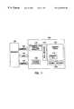
- FIG. 1is a simplified schematic/block diagram illustrating generally one embodiment of a memory including reduced barrier energy floating electrode memory cells.
- FIG. 2is a cross-sectional view that illustrates generally a floating gate transistor embodiment of a memory cell provided by the present invention.
- FIG. 3is an energy band diagram that illustrates generally conduction band energy levels in a floating gate transistor provided by the present invention.
- FIG. 4is a graph comparing barrier energy vs. tunneling distance for a conventional floating gate transistor and one embodiment of a the present invention having a lower barrier energy.
- FIG. 5is a graph that illustrates generally the relationship between Fowler-Nordheim tunneling current density vs. the barrier energy ⁇ GI at various parameterized values E 1 ⁇ E 2 ⁇ E 3 of an electric field.
- FIG. 6illustrates generally how the barrier energy affects the time needed to perform write and erase operations by Fowler-Nordheim tunneling for a particular voltage.
- FIG. 7is a graph that illustrates generally charge density vs. write/erase time for thee different embodiments of a floating gate FET.
- FIG. 8is a cross-sectional view, similar to FIG. 2, but having a larger area control gate—floating gate capacitor than the floating gate—substrate capacitor.
- FIG. 9Ais a schematic diagram, labeled prior art, that illustrates generally a conventional DRAM memory cell.
- FIG. 9Bis a schematic diagram that illustrates generally one embodiment of a floating gate FET memory cell according to the present invention.
- wafer and substrate used in the following descriptioninclude any semiconductor-based structure having an exposed surface with which to form the integrated circuit structure of the invention. Wafer and substrate are used interchangeably to refer to semiconductor structures during processing, and may include other layers that have been fabricated thereupon.
- Both wafer and substrateinclude doped and undoped semiconductors, epitaxial semiconductor layers supported by a base semiconductor or insulator, as well as other semiconductor structures well known to one skilled in the art.
- doped and undoped semiconductorsepitaxial semiconductor layers supported by a base semiconductor or insulator, as well as other semiconductor structures well known to one skilled in the art.
- the following detailed descriptionis, therefore, not to be taken in a limiting sense, and the scope of the present invention is defined only by the appended claims.
- the present inventiondiscloses a dynamic electrically alterable programmable read only memory (DEAPROM) cell.
- the memory cellhas a floating electrode, which is defined as an electrode that is “electrically isolated” from conductors and semiconductors by an insulator such that charge storage upon and removal from the floating electrode depends upon charge conduction through the insulator.
- the floating electrodeis a floating gate electrode in a floating gate field-effect transistor, such as used in flash electrically erasable and programmable read only memories (EEPROMs).
- EEPROMselectrically erasable and programmable read only memories
- EEPROMselectrically erasable and programmable read only memories
- a capacitor or any other structure having a floating electrode and adjacent insulatorcould also be used according to the techniques of the present invention described below.
- a barrier energy between the floating electrode and the insulatoris lower than the barrier energy between polycrystalline silicon (polysilicon) and silicon dioxide (SiO 2 ), which is approximately 3.3 eV.
- the shorter retention time of data charges on the floating electrode, resulting from the smaller barrier energyis accommodated by refreshing the data charges on the floating electrode.
- the memoryoperates similar to a memory cell in a dynamic random access memory (DRAM).
- FIG. 1is a simplified schematic/block diagram illustrating generally one embodiment of a memory 100 according to one aspect of the present invention, in which reduced barrier energy floating electrode memory cells are incorporated.
- Memory 100is referred to as a dynamic electrically alterable programmable read only memory (DEAPROM) in this application, but it is understood that memory 100 possesses certain characteristics that are similar to DRAMs and flash EEPROMs, as explained below.
- DRAMsdynamic electrically alterable programmable read only memory
- flash EEPROMflash EEPROM
- Memory 100includes a memory array 105 of multiple memory cells 110 .
- Row decoder 115 and column decoder 120decode addresses provided on address lines 125 to access the addressed memory cells in memory array 105 .
- Command and control circuitry 130controls the operation of memory 100 in response to control signals received on control lines 135 from a processor 140 or other memory controller during read, write, refresh, and erase operations.
- Command and control circuitry 130includes a refresh circuit for periodically refreshing the data stored on the memory cells 110 .
- Voltage control 150provides appropriate voltages to the memory cells during read, write, refresh, and erase operations.
- Memory 100as illustrated in FIG. 1, has been simplified for the purpose of illustrating the present invention and is not intended to be a complete description. Only the substantial differences between DEAPROM memory 100 and conventional DRAM and flash EEPROM memories are discussed below.
- FIG. 2is a cross-sectional view that illustrates generally, by way of example, but not by way of limitation, one floating gate transistor embodiment of a memory cell 110 .
- Other structural arrangements of floating gate transistorsare included within the present invention.
- any memory cellsthat incorporate a floating electrode (such as a floating electrode capacitor) having, at an interface between the floating electrode an adjacent insulator, a barrier energy that is less than the barrier energy at a polysilicon-SiO 2 interface.
- memory cell 110includes a floating gate FET 200 , which is illustrated as an n-channel FET, but understood to include a p-channel FET embodiment as well.
- FET 200includes a source 205 , a drain 210 , a floating gate 215 electrode, and a control gate 220 electrode.
- a gate insulator 225is interposed between floating gate 215 and substrate 230 .
- An intergate insulator 235is interposed between floating gate 215 and control gate 220 .
- substrate 230is a bulk semiconductor, such as silicon.
- substrate 230includes a thin semiconductor surface layer formed on an underlying insulating portion, such as in a semiconductor-on-insulator (SOI) or other thin film transistor technology.
- Source 205 and drain 210are formed by conventional complementary metal-oxide-semiconductor (CMOS) processing techniques.
- Source 205 and drain 210are separated by a predetermined length for forming an inversion channel 240 therebetween.
- CMOScomplementary metal-oxide-semiconductor
- FIG. 3is an energy band diagram that illustrates generally the conduction band energy levels in floating gate 215 , gate insulator 225 , and substrate 230 .
- Electron affinities ⁇ 215 , ⁇ 225 and ⁇ 230describe floating gate 215 , gate insulator 225 , and substrate 230 , respectively, when measured with respect to a vacuum level 300 .
- a barrier energy ⁇ GIwhich describes the barrier energy at the interface between floating gate 215 and gate insulator 225 ; is given by a difference in electron affinities, as illustrated in Equation 1.
- ⁇ GI⁇ 215 ⁇ 225 (1)
- a barrier energy, ⁇ SGwhich describes the barrier energy at the interface between substrate 230 and gate insulator 225 , is given by a difference in electron affinities, as illustrated in Equation 2.
- Silicon(monocrystalline or polycrystalline Si) has an electron affinity ⁇ 215 ⁇ 4.2 eV.
- Silicon dioxide (SiO 2 )has an electron affinity, ⁇ 225 , of about 0.9 eV.
- the resulting barrier energy at a conventional Si—SiO 2 interface between a floating gate and a gate insulatoris approximately equal to 3.3 eV.
- One aspect of the present inventionprovides a barrier energy ⁇ GI that is less than the 3.3 eV barrier energy of a conventional Si—SiO 2 interface.
- the interface between floating gate 215 and gate insulator 225provides a smaller barrier energy ⁇ GI than the 3.3 eV barrier energy at an interface between polysilicon and silicon dioxide, such as by an appropriate selection of the material composition of one or both of floating gate 215 and gate insulator 225 .
- the smaller barrier energy ⁇ GIis obtained by forming floating gate 215 from a material having a smaller electron affinity ⁇ 215 than polysilicon.
- polycrystalline or microcrystalline silicon carbide (SiC)is used as the material for forming floating gate 215 .
- the smaller barrier energy ⁇ GIis obtained by forming gate insulator 225 from a material having a higher electron affinity ⁇ 225 than SiO 2 .
- amorphous SiCis used as the material for forming gate insulator 225 .
- the smaller barrier energy ⁇ GIis obtained by a combination of forming floating gate 215 from a material having a smaller electron affinity ⁇ 215 than polysilicon and also forming gate insulator 225 from a material having a higher electron affinity ⁇ 225 than SiO 2 .
- the smaller barrier energy ⁇ GIprovides current conduction across gate insulator 225 that is easier than for a polysilicon-SiO 2 interface.
- the present inventionincludes any mechanism of providing such easier current conduction across gate insulator 225 , including, but not limited to “hot” electron injection, thermionic emission, Schottky emission, Frenkel-Poole emission, and Fowler-Nordheim tunneling.
- Such techniques for transporting charge carriers across an insulator, such as gate insulator 225are all enhanced by providing a smaller barrier energy ⁇ GI according to the techniques of the present invention.
- FIG. 4is a graph illustrating generally barrier energy versus tunneling distance for a conventional polysilicon-SiO 2 interface having a 3.3 eV barrier energy.
- FIG. 4also illustrates barrier energy versus tunneling distance for an interface according to the present invention that has a barrier energy of ⁇ GI ⁇ 1.08 eV, which is selected as an illustrative example, and not by way of limitation.
- the smaller barrier energy ⁇ GIreduces the energy to which the electrons must be excited to be stored on or removed from the floating gate 215 , such as by thermal emission over the barrier.
- the smaller barrier energy ⁇ GIalso reduces the distance that electrons have to traverse, such as by Fowler-Nordheim tunneling, to be stored upon or removed from floating gate 215 .
- “do”represents the tunneling distance of a conventional floating gate transistor due to the 3.3 eV barrier energy represented by the dashed line “OLD”.
- the tunneling distance “dn”corresponds to a floating gate transistor according to the present invention and its smaller barrier energy, such as ⁇ GI ⁇ 1.08 eV, for example, represented by the dashed line “NEW”.
- Even a small reduction in the tunneling distanceresults in a large increase in the tunneling probability, as described below, because the tunneling probability is an exponential function of the reciprocal of the tunneling distance.
- Equation 3J is the current density in units of amperes/cm 2
- Eis the electric field in gate insulator 225 in units of volts/cm
- a and Bare constants, which are particular to the material of gate insulator 225 , that depend on the effective electron mass in the gate insulator 225 material and on the barrier energy ⁇ GI .
- the constants A and Bscale with the barrier energy ⁇ GI , as illustrated approximately by Equations 4 and 5, which are disclosed in S. R. Pollack et al., “Electron Transport Through Insulating Thin Films,” Applied Solid State Science, Vol. 1, Academic Press, New York, (1969), p. 354.
- B⁇ ⁇ ⁇ ⁇ ( ⁇ G ⁇ ⁇ I ) 3 2 ( 5 )
- One aspect of the present inventionincludes selecting a smaller barrier energy ⁇ GI such as, by way of example, but not by way of limitation ⁇ GI ⁇ 1.08 eV.
- the constants A and B for ⁇ GI ⁇ 1.08 eVcan be extrapolated from the constants A and B for the 3.3 eV polysilicon-SiO 2 barrier energy using Equations 4 and 5.
- FIG. 5is a graph that illustrates generally the relationship between Fowler-Nordheim tunneling current density vs. the barrier energy ⁇ GI , such as at various parameterized values E 1 ⁇ E 2 ⁇ E 3 of an electric field in gate insulator 225 .
- the tunneling current densityincreases as electric field is increased.
- the tunneling currentalso increases by orders of magnitude as the barrier energy ⁇ GI is decreased, such as by selecting the materials for floating gate 215 and gate insulator 225 or otherwise reducing the barrier energy ⁇ GI according to the techniques of the present invention.
- FIG. 5is a graph that illustrates generally the relationship between Fowler-Nordheim tunneling current density vs. the barrier energy ⁇ GI , such as at various parameterized values E 1 ⁇ E 2 ⁇ E 3 of an electric field in gate insulator 225 .
- the tunneling current densityincreases as electric field is increased.
- the tunneling currentalso increases by orders of magnitude as the barrier energy ⁇ GI is decreased, such as
- FIG. 5illustrates a comparison between tunneling current densities at the 3.3 eV barrier energy of a conventional polysilicon-SiO 2 interface and at the illustrative example barrier energy ⁇ GI ⁇ 1.08 eV for which constants A and B were extrapolated above. Reducing the 3.3 eV barrier energy to ⁇ GI ⁇ 1.08 eV increases the tunneling current density by several orders of magnitude.
- FIG. 6is a conceptual diagram, using rough order of magnitude estimates, that illustrates generally how the barrier energy affects the time needed to perform write and erase operations by Fowler-Nordheim tunneling for a particular voltage, such as across gate insulator 225 .
- FIG. 6also illustrates how the barrier energy affects data charge retention time, such as on floating gate 215 at a temperature of 250 degrees Celsius.
- Both write and erase time 600 and data charge retention time 605are decreased by orders of magnitude as the barrier energy is decreased, according to the present invention, from the conventional polysilicon-SiO 2 interface barrier energy of 3.3 eV to the illustrative example lower barrier energy ⁇ GI ⁇ 1.08 eV for which constants A and B were extrapolated above.
- the lower barrier energy ⁇ GI and increased tunneling currentadvantageously provides faster write and erase times. This is particularly advantageous for “flash” EEPROMs or DEAPROMs in which many floating gate transistor memory cells must be erased simultaneously, requiring a longer time to transport the larger quantity of charge.
- flash EEPROMs or DEAPROMsin which many floating gate transistor memory cells must be erased simultaneously, requiring a longer time to transport the larger quantity of charge.
- the simultaneous erasure of a block of memory cellsrequires a time that is on the order of milliseconds.
- the write and erase time of the floating gate FET 200is illustrated approximately by Equation 6.
- Equation 6t is the write/erase time, J 225 and J 235 are the respective tunneling current densities in gate dielectric 225 and intergate dielectric 235 , Q is the charge density in Coulombs/cm 2 on floating gate 215 . Equation 6 is evaluated for a specific voltage on control gate 220 using Equations 7 and 8.
- E 225V 220 [ d 225 + d 235 ⁇ ( ⁇ 225 ⁇ 235 ) ] - Q [ ⁇ 225 + ⁇ 235 ⁇ ( d 225 d 235 ) ] ( 7 )
- E 235V 220 [ d 235 + d 225 ⁇ ( ⁇ 235 ⁇ 225 ) ] + Q [ ⁇ 235 + ⁇ 225 ⁇ ( d 235 d 225 ) ] ( 8 )
- V 220is the voltage on control gate 220
- E 225 and E 235are the respective electric fields in gate insulator 225 and intergate insulator 235
- d 225 and d 235are the respective thicknesses of gate insulator 225 and intergate insulator 235
- ⁇ 225 and ⁇ 235are the respective permittivities of gate insulator 225 and intergate insulator 235 .
- FIG. 7is a graph that illustrates generally charge density vs. write/erase time for three different embodiments of the floating gate FET 200 , each of which have a polysilicon floating gate 215 , by way of illustrative example.
- Line 700illustrates generally, by way of example, but not by way of limitation, the charge density vs. write/erase time obtained for a floating gate FET 200 having a 100 ⁇ SiO 2 gate insulator 225 and a 150 ⁇ SiO 2 (or thinner oxynitride equivalent capacitance) intergate insulator 235 .
- Line 705is similar to line 700 in all respects except that line 705 illustrates a floating gate FET 200 in which gate insulator 225 comprises a material having a higher electron affinity ⁇ 225 than SiO 2 , thereby providing a lower barrier energy ⁇ GI at the interface between polysilicon floating gate 215 and gate insulator 225 .
- the increased tunneling currentresults in shorter write/erase times than those illustrated by line 700 .
- Line 710is similar to line 705 in all respects except that line 710 illustrates a floating gate FET 200 in which gate insulator 225 has a lower barrier energy ⁇ GI than for line 705 , or intergate insulator 235 has a higher permittivity ⁇ 235 than for line 705 , or control gate 220 has a larger area than floating gate 215 , such as illustrated by way of example by the floating gate FET 800 in the cross-sectional view of FIG. 8 . As seen in FIG.
- the area of a capacitor formed by the control gate 220 , the floating gate 215 , and the intergate insulator 235is larger than the area of a capacitor formed by the floating gate 215 , the gate insulator 225 , and the inversion channel 240 underlying gate insulator 225 .
- the intergate insulator 235can have a higher permittivity than the permittivity of silicon dioxide.
- the barrier energy ⁇ GIcan be selected to reduce the write/erase time.
- the barrier energy ⁇ GIis selected to obtain a write/erase time of less than or equal to 1 second, as illustrated in FIG. 7 .
- the barrier energy ⁇ GIis selected to obtain a write/erase time of less than or equal to 1 millisecond, as illustrated in FIG. 7 .
- Other values of write/erase timecan also be obtained by selecting the appropriate value of the barrier energy ⁇ GI .
- the lower barrier energy ⁇ GI and increased tunneling currentalso advantageously reduces the voltage required for writing and erasing the memory cells 110 .
- conventional polysilicon floating gate transistorstypically require complicated and noisy on-chip charge pump circuits to generate the large erasure voltage, which typically far exceeds other voltages required on the integrated circuit
- the present inventionallows the use of lower erasure voltages that are more easily provided by simpler on-chip circuits. Reducing the erasure voltage also lowers the electric fields, minimizing reliability problems that can lead to device failure, and better accommodating downward scaling of device dimensions.
- the barrier energy ⁇ GIis selected, as described above, to obtain an erase voltage of less than the 12 Volts required by typical EEPROM memory cells.
- the thickness of the gate insulator 225can be increased from the typical thickness of a silicon dioxide gate insulator to improve reliability or simplify processing, since the lower barrier energy ⁇ GI allows easier transport of charge across the gate insulator 225 by Fowler-Nordheim tunneling.
- the lower barrier energy ⁇ GIalso decreases the data charge retention time of the charge stored on the floating gate 215 , such as from increased thermal excitation of stored charge over the lower barrier ⁇ GI .
- conventional polysilicon floating gates and adjacent SiO 2 insulatorse.g., 90 ⁇ thick
- the barrier energy ⁇ GIis lowered to ⁇ GI ⁇ 1.08 eV by appropriately selecting the composition of the materials of floating gate 215 and gate insulator 225 , as described below.
- an estimated data charge retention timeof approximately 40 seconds at a high temperature, such as 250 degrees C., is obtained.
- the data stored on the memory cell 110is periodically refreshed at an interval that is shorter than the data charge retention time.
- the datais refreshed every few seconds, such as for an embodiment having a high temperature retention time of approximately 40 seconds for ⁇ GI ⁇ 1.08 eV.
- the exact refresh ratecan be experimentally determined and tailored to a particular process of fabricating the DEAPROM. By decreasing the data charge retention time and periodically refreshing the data, the write and erase operations can be several orders of magnitude faster, as described above with respect to FIG. 7 .
- FIGS. 9A and 9Bare schematic diagrams that respectively illustrate generally a conventional DRAM memory cell and the present invention's floating gate FET 200 embodiment of memory cell 110 .
- the DRAM memory cellincludes an access FET 900 and stacked or trench storage capacitor 905 .
- Datais stored as charge on storage capacitor 905 by providing a control voltage on control line 910 to activate FET 900 for conducting charge.
- Data line 915provides a write voltage to conduct charge across FET 900 for storage on storage capacitor 905 .
- Datais read by providing a control voltage on control line 910 to activate FET 900 for conducting charge from storage capacitor 905 , thereby incrementally changing a preinitialized voltage on data line 915 .
- the resulting small change in voltage on data line 915must be amplified by a sense amplifier for detection.
- the DRAM memory cell of FIG. 9Ainherently provides only a small data signal. The small data signal is difficult to detect.
- the memory cell 110is a DEAPROM memory cell that includes floating gate FET 200 , having source 205 coupled to a ground voltage or other reference potential. Data is stored as charge on floating gate 215 by providing a control voltage on control line 920 and a write voltage on data line 925 for hot electron injection or Fowler-Nordheim tunneling. This is similar to conventional EEPROM techniques, but advantageously uses the reduced voltages and/or a shorter write time of the present invention.
- the DEAPROM memory cellcan be smaller than the DRAM memory cell of FIG. 9A, allowing higher density data storage.
- the leakage of charge from floating gate 215can be made less than the reverse-bias junction leakage from storage capacitor 905 of the DRAM memory cell by tailoring the barrier energy ⁇ GI according to the techniques of the present invention.
- the DEAPROM memory celladvantageously uses the large transconductance gain of the floating gate FET 200 .
- the conventional DRAM memory cell of FIG. 9Aprovides no such gain; it is read by directly transferring the data charge from storage capacitor 905 .
- the DEAPROM memory cellis read by placing a read voltage on control line 920 , and detecting the current conducted through FET 200 , such as at data line 925 .
- the current conducted through FET 200changes significantly in the presence or absence of charge stored on floating gate 215 .
- the present inventionadvantageously provides an large data signal that is easy to detect, unlike the small data signal provided by the conventional DRAM memory cell of FIG. 9 A.
- Equation 9the current for floating gate FET 200 operating in the saturation region can be approximated by Equation 9.
- I D ⁇ ⁇ S1 2 ⁇ ⁇ ⁇ ⁇ C o ⁇ ( W L ) ⁇ ⁇ ( V G - V T ) 2 ( 9 )
- I DSis the current between drain 210 and source 205
- C ois the capacitance per unit area of the gate insulator 225
- W/Lis the width/length aspect ratio of FET 200
- V Gis the gate voltage applied to control gate 220
- V Tis the turn-on threshold voltage of FET 200 .
- sufficient chargeis stored on floating gate 215 to change the effective threshold voltage V T by approximately 1.4 Volts, thereby changing the current I DS by approximately 100 microamperes.
- This significant change in currentcan easily be detected, such as by sampling or integrating over a time period of approximately 10 nanoseconds, for example, to obtain a detected data charge signal of 1000 fC.
- the DEAPROM memory cellis capable of yielding a detected data charge signal that is approximately an order of magnitude larger than the typical 30 fC to 100 fC data charges typically stored on DRAM stacked or trench capacitors. Since DEAPROM memory cell requires a smaller capacitance value than a conventional DRAM memory cell, DEAPROM memory cell can be made smaller than a conventional DRAM memory cell. Moreover, because the CMOS-compatible DEAPROM storage capacitor is integrally formed as part of the transistor, rather than requiring complex and costly non-CMOS stacked and trench capacitor process steps, the DEAPROM memory of the present invention should be cheaper to fabricate than DRAM memory cells, and should more easily scale downward as CMOS technology advances.
- the present inventionprovides a DEAPROM having a memory cell 110 including a FET 200 having an at least partially crystalline (e.g., monocrystalline, polycrystalline, microcrystalline, nanocrystalline, or combination thereof) gallium nitride (GaN) or gallium aluminum nitride (GaAlN) floating gate 215 .
- a DEAPROMhaving a memory cell 110 including a FET 200 having an at least partially crystalline (e.g., monocrystalline, polycrystalline, microcrystalline, nanocrystalline, or combination thereof) gallium nitride (GaN) or gallium aluminum nitride (GaAlN) floating gate 215 .
- GaNgallium nitride
- GaAlNgallium aluminum nitride
- a composition v of a polycrystalline Ga 1 ⁇ v Al v N floating gate 215is selected approximately between 0 ⁇ v ⁇ 1 to obtain a desired barrier energy, as described below.
- the GaAlN floating gate 215provides a lower electron affinity than polysilicon.
- the GaAlN floating gate 215 electron affinitycan be approximately between 0.6 eV ⁇ 215 ⁇ 2.7 eV as the GaAlN composition variable v is decreased from 1 to 0. See V. M. Bermudez et al. “The Growth and Properties of Al and AlN films on GaN” J. Appl. Physics. Vol. 79, No. 1, pp. 110-119 (1996).
- the GaAlN floating gate 215provides a smaller resulting barrier energy ⁇ GI than a polysilicon gate material having an electron affinity ⁇ 215 ⁇ 4.2 eV.
- a barrier energy approximately between ⁇ 0.3 eV ⁇ GI ⁇ 1.8 eVis obtained using an GaAlN floating gate 215 as the GaAlN composition v varies between v ⁇ 1 (i.e., approximately AlN) and v ⁇ 0 (i.e., approximately GaN).
- a conventional polysilicon floating gate materialprovides a barrier energy ⁇ GI ⁇ 3.3 eV at an interface with an SiO 2 gate insulator 225 .
- substrate 230is bulk silicon, although other bulk semiconductor and semiconductor-on-insulator (SOI) materials could also be used for substrate 230 such as, for example, sapphire, gallium arsenide (GaAs), GaN, AlN, and diamond.
- gate insulator 225is SiO 2 , although other dielectric materials could also be used for gate insulator 225 , as described above, such as amorphous insulating GaN (a-GaN), and amorphous insulating AlN (a-AlN).
- the FET 200 using a GaAlN floating gate 215has mobility and turn-on threshold voltage (V T ) magnitude parameters that are advantageously influenced less by charge at SiO 2 -GaAlN interface surface states than at a conventional SiO 2 -polysilicon interface.
- floating gate 215is formed of a polycrystalline, microcrystalline, or nanocrystalline, GaN thin film that is CVD deposited on a thin (e.g., 500 ⁇ thick) AlN buffer layer, such as by metal organic chemical vapor deposition (MOCVD), which advantageously yields improved crystal quality and reduced microscopic fluctuation of crystallite orientation.
- MOCVDmetal organic chemical vapor deposition
- floating gate 215is formed from a GaN film grown in a horizontal reactor operating at atmospheric pressure.
- Trimethyl gallium (TMG), timethylaluminum (TMA) and ammonia (NH 3 )are used as source gases, and hydrogen (H 2 ) is used as a carrier gas.
- the TMG, TMA and NH 3are mixed just before the reactor, and the mixture is fed at high velocity (e.g., 110 cm/s) to a slanted substrate 230 through a delivery tube.
- the desired GaAlN composition vis obtained by controlling the concentration ratio of TMG to TMA.
- a 500 ⁇ AlN buffer layeris obtained by growth at 600 degrees Celsius at a deposition rate of 100 ⁇ /minute for approximately 5 minutes, then a epitaxial crystalline or polycrystalline layer of GaN is deposited at 1000 degrees Celsius.
- PEMBEplasma enhanced molecular beam epitaxy
- ECRelectron cyclotron resonance
- MBEmolecular beam epitaxy
- the background pressure in the MBE chamberis typically less than 10 ⁇ 10 torr.
- Ga flux(e.g., 99.99999% pure) is supplied by a conventional Knudsen effusion cell.
- the semiconductor substrates 230are heated to a temperature of approximately 850 degrees Celsius, and exposed to a nitrogen plasma (e.g., 35 Watt plasma power level) to clean the surface of the substrate 230 and form a thin AlN layer thereupon.
- the temperatureis then lowered to approximately 550 degrees Celsius for growth of a thin (e.g., 300 ⁇ ) GaN buffer layer (e.g., using 20 Watt plasma power level for growth in a low active nitrogen overpressure environment).
- the temperatureis then increased, such as to approximately 800 degrees Celsius, to form the remainder of the GaN or GaAlN film forming floating gate 215 , such as at a deposition rate of approximately 0.22 microns/hour.
- the present inventionprovides a DEAPROM cell.
- the memory cellhas a gallium nitride (GaN) or gallium aluminum nitride (GaAlN) floating electrode, such as a floating gate electrode in a floating gate field-effect transistor.
- a barrier energy between the floating electrode and the insulatoris lower than the barrier energy between polysilicon and SiO 2 , which is approximately 3.3 eV.
- the memory cellalso provides large transconductance gain, which provides a more easily detected signal and reduces the required data storage capacitance value.
- the shorter retention time of data charges on the floating electrode, resulting from the smaller barrier energyis accommodated by refreshing the data charges on the floating electrode.
- the memoryoperates similar to a memory cell in DRAM, but avoids the process complexity, additional space needed, and other limitations of forming stacked or trench DRAM capacitors.
Landscapes
- Engineering & Computer Science (AREA)
- Microelectronics & Electronic Packaging (AREA)
- Non-Volatile Memory (AREA)
- Semiconductor Memories (AREA)
- Read Only Memory (AREA)
Abstract
Description


Claims (37)
Priority Applications (2)
| Application Number | Priority Date | Filing Date | Title |
|---|---|---|---|
| US09/141,392US6249020B1 (en) | 1997-07-29 | 1998-08-27 | DEAPROM and transistor with gallium nitride or gallium aluminum nitride gate |
| US09/883,795US7005344B2 (en) | 1997-07-29 | 2001-06-18 | Method of forming a device with a gallium nitride or gallium aluminum nitride gate |
Applications Claiming Priority (2)
| Application Number | Priority Date | Filing Date | Title |
|---|---|---|---|
| US08/902,098US6031263A (en) | 1997-07-29 | 1997-07-29 | DEAPROM and transistor with gallium nitride or gallium aluminum nitride gate |
| US09/141,392US6249020B1 (en) | 1997-07-29 | 1998-08-27 | DEAPROM and transistor with gallium nitride or gallium aluminum nitride gate |
Related Parent Applications (1)
| Application Number | Title | Priority Date | Filing Date |
|---|---|---|---|
| US08/902,098DivisionUS6031263A (en) | 1997-07-29 | 1997-07-29 | DEAPROM and transistor with gallium nitride or gallium aluminum nitride gate |
Related Child Applications (1)
| Application Number | Title | Priority Date | Filing Date |
|---|---|---|---|
| US09/883,795DivisionUS7005344B2 (en) | 1997-07-29 | 2001-06-18 | Method of forming a device with a gallium nitride or gallium aluminum nitride gate |
Publications (1)
| Publication Number | Publication Date |
|---|---|
| US6249020B1true US6249020B1 (en) | 2001-06-19 |
Family
ID=25415307
Family Applications (5)
| Application Number | Title | Priority Date | Filing Date |
|---|---|---|---|
| US08/902,098Expired - LifetimeUS6031263A (en) | 1997-07-29 | 1997-07-29 | DEAPROM and transistor with gallium nitride or gallium aluminum nitride gate |
| US09/140,978Expired - LifetimeUS6307775B1 (en) | 1997-07-29 | 1998-08-27 | Deaprom and transistor with gallium nitride or gallium aluminum nitride gate |
| US09/141,392Expired - LifetimeUS6249020B1 (en) | 1997-07-29 | 1998-08-27 | DEAPROM and transistor with gallium nitride or gallium aluminum nitride gate |
| US09/883,795Expired - Fee RelatedUS7005344B2 (en) | 1997-07-29 | 2001-06-18 | Method of forming a device with a gallium nitride or gallium aluminum nitride gate |
| US10/047,181Expired - Fee RelatedUS6781876B2 (en) | 1997-07-29 | 2001-10-23 | Memory device with gallium nitride or gallium aluminum nitride gate |
Family Applications Before (2)
| Application Number | Title | Priority Date | Filing Date |
|---|---|---|---|
| US08/902,098Expired - LifetimeUS6031263A (en) | 1997-07-29 | 1997-07-29 | DEAPROM and transistor with gallium nitride or gallium aluminum nitride gate |
| US09/140,978Expired - LifetimeUS6307775B1 (en) | 1997-07-29 | 1998-08-27 | Deaprom and transistor with gallium nitride or gallium aluminum nitride gate |
Family Applications After (2)
| Application Number | Title | Priority Date | Filing Date |
|---|---|---|---|
| US09/883,795Expired - Fee RelatedUS7005344B2 (en) | 1997-07-29 | 2001-06-18 | Method of forming a device with a gallium nitride or gallium aluminum nitride gate |
| US10/047,181Expired - Fee RelatedUS6781876B2 (en) | 1997-07-29 | 2001-10-23 | Memory device with gallium nitride or gallium aluminum nitride gate |
Country Status (1)
| Country | Link |
|---|---|
| US (5) | US6031263A (en) |
Cited By (38)
| Publication number | Priority date | Publication date | Assignee | Title |
|---|---|---|---|---|
| US20030001191A1 (en)* | 1997-07-29 | 2003-01-02 | Micron Technology, Inc. | Dynamic electrically alterable programmable read only memory device |
| US20030042528A1 (en)* | 2001-08-30 | 2003-03-06 | Leonard Forbes | Sram cells with repressed floating gate memory, low tunnel barrier interpoly insulators |
| US20030042534A1 (en)* | 2001-08-30 | 2003-03-06 | Micron Technology, Inc. | Scalable flash/NV structures and devices with extended endurance |
| US20030048666A1 (en)* | 2001-08-30 | 2003-03-13 | Micron Technology, Inc. | Graded composition metal oxide tunnel barrier interpoly insulators |
| US6586797B2 (en) | 2001-08-30 | 2003-07-01 | Micron Technology, Inc. | Graded composition gate insulators to reduce tunneling barriers in flash memory devices |
| US20030235066A1 (en)* | 2002-06-21 | 2003-12-25 | Micron Technology, Inc. | Ferroelectric write once read only memory for archival storage |
| US20030235079A1 (en)* | 2002-06-21 | 2003-12-25 | Micron Technology, Inc. | Nor flash memory cell with high storage density |
| US20030235085A1 (en)* | 2002-06-21 | 2003-12-25 | Micron Technology, Inc. | Write once read only memory employing charge trapping in insulators |
| US20030235081A1 (en)* | 2002-06-21 | 2003-12-25 | Micron Technology, Inc. | Nanocrystal write once read only memory for archival storage |
| US20030234420A1 (en)* | 2002-06-21 | 2003-12-25 | Micron Technology, Inc. | Write once read only memory with large work function floating gates |
| US20040004859A1 (en)* | 2002-07-08 | 2004-01-08 | Micron Technology, Inc. | Memory utilizing oxide nanolaminates |
| US20040042256A1 (en)* | 2002-08-29 | 2004-03-04 | Micron Technology, Inc. | Single transistor vertical memory gain cell |
| US20040041236A1 (en)* | 2002-08-29 | 2004-03-04 | Micron Technology, Inc. | Merged mos-bipolar capacitor memory cell |
| US6754108B2 (en) | 2001-08-30 | 2004-06-22 | Micron Technology, Inc. | DRAM cells with repressed floating gate memory, low tunnel barrier interpoly insulators |
| US20040151029A1 (en)* | 1999-08-26 | 2004-08-05 | Micron Technology, Inc. | Programmable memory cell using charge trapping in a gate oxide |
| US20040183073A1 (en)* | 2003-03-17 | 2004-09-23 | Shuo Gu | Large grain size polysilicon films formed by nuclei-induced solid phase crystallization |
| US6804142B2 (en) | 2002-11-12 | 2004-10-12 | Micron Technology, Inc. | 6F2 3-transistor DRAM gain cell |
| US20050012141A1 (en)* | 2002-02-12 | 2005-01-20 | Micron Technology, Inc. | Asymmetric band-gap engineered nonvolatile memory device |
| US20050023595A1 (en)* | 2001-08-30 | 2005-02-03 | Micron Technology, Inc. | Programmable array logic or memory devices with asymmetrical tunnel barriers |
| US20050023574A1 (en)* | 2002-07-08 | 2005-02-03 | Micron Technology, Inc. | Memory utilizing oxide-nitride nanolaminates |
| US20050023602A1 (en)* | 2001-08-30 | 2005-02-03 | Micron Technology, Inc. | Programmable array logic or memory with p-channel devices and asymmetrical tunnel barriers |
| US20050024936A1 (en)* | 2003-03-04 | 2005-02-03 | Micron Technology, Inc. | Vertical gain cell |
| US20050024945A1 (en)* | 2001-08-30 | 2005-02-03 | Micron Technology, Inc. | Programmable memory address and decode circuits with low tunnel barrier interpoly insulators |
| US20050146934A1 (en)* | 1997-07-29 | 2005-07-07 | Micron Technology, Inc. | Transistor with variable electron affinity gate and methods of fabrication and use |
| US6956772B2 (en) | 2001-02-13 | 2005-10-18 | Micron Technology, Inc. | Programmable fuse and antifuse and method thereof |
| US20060002192A1 (en)* | 2001-08-30 | 2006-01-05 | Micron Technology | Integrated circuit memory device and method |
| US20060001049A1 (en)* | 2001-08-30 | 2006-01-05 | Micron Technology, Inc. | Service programmable logic arrays with low tunnel barrier interpoly insulators |
| US20060017095A1 (en)* | 1997-07-29 | 2006-01-26 | Micron Technology, Inc. | Carburized silicon gate insulators for integrated circuits |
| US20060024878A1 (en)* | 1997-07-29 | 2006-02-02 | Micron Technology, Inc. | Deaprom having amorphous silicon carbide gate insulator |
| US7068544B2 (en) | 2001-08-30 | 2006-06-27 | Micron Technology, Inc. | Flash memory with low tunnel barrier interpoly insulators |
| US20060199338A1 (en)* | 2001-08-30 | 2006-09-07 | Micron Technology, Inc. | Atomic layer deposition of metal oxide and/or low asymmetrical tunnel barrier interpoly insulators |
| US7130220B2 (en) | 2002-06-21 | 2006-10-31 | Micron Technology, Inc. | Write once read only memory employing floating gates |
| US20070258306A1 (en)* | 2006-05-05 | 2007-11-08 | Honeywell International Inc. | Method for Refreshing a Non-Volatile Memory |
| US7429515B2 (en) | 2001-12-20 | 2008-09-30 | Micron Technology, Inc. | Low-temperature grown high quality ultra-thin CoTiO3 gate dielectrics |
| US7687848B2 (en) | 2002-07-08 | 2010-03-30 | Micron Technology, Inc. | Memory utilizing oxide-conductor nanolaminates |
| US7709402B2 (en) | 2006-02-16 | 2010-05-04 | Micron Technology, Inc. | Conductive layers for hafnium silicon oxynitride films |
| US20110132448A1 (en)* | 2010-02-08 | 2011-06-09 | Suniva, Inc. | Solar cells and methods of fabrication thereof |
| US8501563B2 (en) | 2005-07-20 | 2013-08-06 | Micron Technology, Inc. | Devices with nanocrystals and methods of formation |
Families Citing this family (75)
| Publication number | Priority date | Publication date | Assignee | Title |
|---|---|---|---|---|
| US6746893B1 (en) | 1997-07-29 | 2004-06-08 | Micron Technology, Inc. | Transistor with variable electron affinity gate and methods of fabrication and use |
| US6031263A (en)* | 1997-07-29 | 2000-02-29 | Micron Technology, Inc. | DEAPROM and transistor with gallium nitride or gallium aluminum nitride gate |
| US6936849B1 (en) | 1997-07-29 | 2005-08-30 | Micron Technology, Inc. | Silicon carbide gate transistor |
| US6768165B1 (en) | 1997-08-01 | 2004-07-27 | Saifun Semiconductors Ltd. | Two bit non-volatile electrically erasable and programmable semiconductor memory cell utilizing asymmetrical charge trapping |
| US6133634A (en)* | 1998-08-05 | 2000-10-17 | Fairchild Semiconductor Corporation | High performance flip chip package |
| US6531751B1 (en)* | 1998-12-03 | 2003-03-11 | Agere Systems Inc. | Semiconductor device with increased gate insulator lifetime |
| US6495409B1 (en)* | 1999-01-26 | 2002-12-17 | Agere Systems Inc. | MOS transistor having aluminum nitride gate structure and method of manufacturing same |
| US6352944B1 (en)* | 1999-02-10 | 2002-03-05 | Micron Technology, Inc. | Method of depositing an aluminum nitride comprising layer over a semiconductor substrate |
| US6384448B1 (en) | 2000-02-28 | 2002-05-07 | Micron Technology, Inc. | P-channel dynamic flash memory cells with ultrathin tunnel oxides |
| US6249460B1 (en) | 2000-02-28 | 2001-06-19 | Micron Technology, Inc. | Dynamic flash memory cells with ultrathin tunnel oxides |
| US6639835B2 (en) | 2000-02-29 | 2003-10-28 | Micron Technology, Inc. | Static NVRAM with ultra thin tunnel oxides |
| US6677640B1 (en) | 2000-03-01 | 2004-01-13 | Micron Technology, Inc. | Memory cell with tight coupling |
| US6313487B1 (en) | 2000-06-15 | 2001-11-06 | Board Of Regents, The University Of Texas System | Vertical channel floating gate transistor having silicon germanium channel layer |
| US6313486B1 (en) | 2000-06-15 | 2001-11-06 | Board Of Regents, The University Of Texas System | Floating gate transistor having buried strained silicon germanium channel layer |
| US6576932B2 (en) | 2001-03-01 | 2003-06-10 | Lumileds Lighting, U.S., Llc | Increasing the brightness of III-nitride light emitting devices |
| DE10120877A1 (en)* | 2001-04-27 | 2002-10-31 | Philips Corp Intellectual Pty | Arrangement with a semiconductor device |
| KR100422565B1 (en) | 2001-06-12 | 2004-03-12 | 주식회사 하이닉스반도체 | Method of forming a capacitor of a semiconductor device |
| KR100410389B1 (en) | 2001-06-12 | 2003-12-18 | 주식회사 하이닉스반도체 | Method of forming a capacitor of a semiconductor device |
| KR100418580B1 (en) | 2001-06-12 | 2004-02-21 | 주식회사 하이닉스반도체 | Method of forming a capacitor of a semiconductor device |
| DE10228768A1 (en)* | 2001-06-28 | 2003-01-16 | Samsung Electronics Co Ltd | Non-volatile floating trap storage device comprises a semiconductor substrate, a tunnel insulation layer on the substrate, a charge storage layer, a barrier insulation layer, and a gate electrode |
| US8253183B2 (en) | 2001-06-28 | 2012-08-28 | Samsung Electronics Co., Ltd. | Charge trapping nonvolatile memory devices with a high-K blocking insulation layer |
| US7473959B2 (en)* | 2001-06-28 | 2009-01-06 | Samsung Electronics Co., Ltd. | Non-volatile semiconductor memory devices and methods of fabricating the same |
| US7253467B2 (en)* | 2001-06-28 | 2007-08-07 | Samsung Electronics Co., Ltd. | Non-volatile semiconductor memory devices |
| US20060180851A1 (en)* | 2001-06-28 | 2006-08-17 | Samsung Electronics Co., Ltd. | Non-volatile memory devices and methods of operating the same |
| US6664589B2 (en) | 2001-08-30 | 2003-12-16 | Micron Technology, Inc. | Technique to control tunneling currents in DRAM capacitors, cells, and devices |
| US6700818B2 (en) | 2002-01-31 | 2004-03-02 | Saifun Semiconductors Ltd. | Method for operating a memory device |
| US6794236B1 (en)* | 2002-06-03 | 2004-09-21 | Lattice Semiconductor Corporation | Eeprom device with improved capacitive coupling and fabrication process |
| US6791883B2 (en)* | 2002-06-24 | 2004-09-14 | Freescale Semiconductor, Inc. | Program and erase in a thin film storage non-volatile memory |
| US6917544B2 (en) | 2002-07-10 | 2005-07-12 | Saifun Semiconductors Ltd. | Multiple use memory chip |
| TWI320571B (en)* | 2002-09-12 | 2010-02-11 | Qs Semiconductor Australia Pty Ltd | Dynamic nonvolatile random access memory ne transistor cell and random access memory array |
| US6830953B1 (en)* | 2002-09-17 | 2004-12-14 | Taiwan Semiconductor Manufacturing Company, Ltd. | Suppression of MOSFET gate leakage current |
| US7229498B2 (en)* | 2002-10-29 | 2007-06-12 | Midwest Research Institute | Nanostructures produced by phase-separation during growth of (III-V)1-x(IV2)x alloys |
| US7136304B2 (en) | 2002-10-29 | 2006-11-14 | Saifun Semiconductor Ltd | Method, system and circuit for programming a non-volatile memory array |
| AU2002368226A1 (en)* | 2002-10-29 | 2004-05-25 | Midwest Research Institute | Nanostructures produced by phase-separation during growth of (iii-v)1-x(iv2)x alloys |
| US7178004B2 (en) | 2003-01-31 | 2007-02-13 | Yan Polansky | Memory array programming circuit and a method for using the circuit |
| US6600673B1 (en) | 2003-01-31 | 2003-07-29 | International Business Machines Corporation | Compilable writeable read only memory (ROM) built with register arrays |
| US7142464B2 (en) | 2003-04-29 | 2006-11-28 | Saifun Semiconductors Ltd. | Apparatus and methods for multi-level sensing in a memory array |
| TWI313060B (en)* | 2003-07-28 | 2009-08-01 | Japan Science & Tech Agency | Feild effect transisitor and fabricating method thereof |
| US7123532B2 (en) | 2003-09-16 | 2006-10-17 | Saifun Semiconductors Ltd. | Operating array cells with matched reference cells |
| KR100562743B1 (en)* | 2003-10-06 | 2006-03-21 | 동부아남반도체 주식회사 | Manufacturing Method of Flash Memory Device |
| DE10349557B4 (en)* | 2003-10-22 | 2010-09-09 | Infineon Technologies Ag | Use of a capacitor arrangement and method for driving |
| KR100539247B1 (en)* | 2004-02-04 | 2005-12-27 | 삼성전자주식회사 | Split gate type non-volatile semiconductor memory device and method of fabricating the same |
| US20050242387A1 (en)* | 2004-04-29 | 2005-11-03 | Micron Technology, Inc. | Flash memory device having a graded composition, high dielectric constant gate insulator |
| US7317633B2 (en) | 2004-07-06 | 2008-01-08 | Saifun Semiconductors Ltd | Protection of NROM devices from charge damage |
| US7095655B2 (en) | 2004-08-12 | 2006-08-22 | Saifun Semiconductors Ltd. | Dynamic matching of signal path and reference path for sensing |
| US7385238B2 (en)* | 2004-08-16 | 2008-06-10 | Micron Technology, Inc. | Low dark current image sensors with epitaxial SiC and/or carbonated channels for array transistors |
| US7638850B2 (en) | 2004-10-14 | 2009-12-29 | Saifun Semiconductors Ltd. | Non-volatile memory structure and method of fabrication |
| WO2006046301A1 (en) | 2004-10-29 | 2006-05-04 | Spansion Llc | Semiconductor device and semiconductor device manufacturing method |
| US7535765B2 (en) | 2004-12-09 | 2009-05-19 | Saifun Semiconductors Ltd. | Non-volatile memory device and method for reading cells |
| EP1686592A3 (en) | 2005-01-19 | 2007-04-25 | Saifun Semiconductors Ltd. | Partial erase verify |
| US7157784B2 (en)* | 2005-01-31 | 2007-01-02 | Texas Instruments Incorporated | Drain extended MOS transistors with multiple capacitors and methods of fabrication |
| US7786512B2 (en) | 2005-07-18 | 2010-08-31 | Saifun Semiconductors Ltd. | Dense non-volatile memory array and method of fabrication |
| JP4537909B2 (en)* | 2005-08-08 | 2010-09-08 | 株式会社東芝 | Information recording device |
| US20070045707A1 (en)* | 2005-08-31 | 2007-03-01 | Szu-Yu Wang | Memory device and manufacturing method thereof |
| US7808818B2 (en) | 2006-01-12 | 2010-10-05 | Saifun Semiconductors Ltd. | Secondary injection for NROM |
| US7692961B2 (en) | 2006-02-21 | 2010-04-06 | Saifun Semiconductors Ltd. | Method, circuit and device for disturb-control of programming nonvolatile memory cells by hot-hole injection (HHI) and by channel hot-electron (CHE) injection |
| US7760554B2 (en) | 2006-02-21 | 2010-07-20 | Saifun Semiconductors Ltd. | NROM non-volatile memory and mode of operation |
| US8253452B2 (en) | 2006-02-21 | 2012-08-28 | Spansion Israel Ltd | Circuit and method for powering up an integrated circuit and an integrated circuit utilizing same |
| US7638835B2 (en) | 2006-02-28 | 2009-12-29 | Saifun Semiconductors Ltd. | Double density NROM with nitride strips (DDNS) |
| US7701779B2 (en) | 2006-04-27 | 2010-04-20 | Sajfun Semiconductors Ltd. | Method for programming a reference cell |
| US7579646B2 (en)* | 2006-05-25 | 2009-08-25 | Taiwan Semiconductor Manufacturing Company, Ltd. | Flash memory with deep quantum well and high-K dielectric |
| US8816422B2 (en)* | 2006-09-15 | 2014-08-26 | Taiwan Semiconductor Manufacturing Company, Ltd. | Multi-trapping layer flash memory cell |
| US7605579B2 (en) | 2006-09-18 | 2009-10-20 | Saifun Semiconductors Ltd. | Measuring and controlling current consumption and output current of charge pumps |
| US8294197B2 (en)* | 2006-09-22 | 2012-10-23 | Taiwan Semiconductor Manufacturing Company, Ltd. | Program/erase schemes for floating gate memory cells |
| KR101338158B1 (en)* | 2007-07-16 | 2013-12-06 | 삼성전자주식회사 | Non-volatile memory devices and methods of forming the same |
| US7791105B2 (en)* | 2008-04-09 | 2010-09-07 | International Business Machines Corporation | Device structures for a high voltage junction field effect transistor manufactured using a hybrid orientation technology wafer and design structures for a high voltage integrated circuit |
| US20090258464A1 (en)* | 2008-04-09 | 2009-10-15 | International Business Machines Corporation | Methods for manufacturing a high voltage junction field effect transistor using a hybrid orientation technology wafer |
| US8735963B2 (en)* | 2008-07-07 | 2014-05-27 | Taiwan Semiconductor Manufacturing Company, Ltd. | Flash memory cells having leakage-inhibition layers |
| JP5257176B2 (en)* | 2009-03-18 | 2013-08-07 | ソニー株式会社 | Solid-state imaging device, driving method of solid-state imaging device, and electronic apparatus |
| JP5427148B2 (en)* | 2010-09-15 | 2014-02-26 | パナソニック株式会社 | Semiconductor device |
| US9123671B2 (en)* | 2010-12-30 | 2015-09-01 | Taiwan Semiconductor Manufacturing Company, Ltd. | Silicon wafer strength enhancement |
| WO2013001579A1 (en)* | 2011-06-30 | 2013-01-03 | パナソニック株式会社 | Thin film transistor device and method for producing thin film transistor device |
| KR101946009B1 (en) | 2012-10-11 | 2019-02-08 | 삼성전자주식회사 | High electron mobility transistor and method of driving the same |
| KR102065113B1 (en) | 2013-05-01 | 2020-01-10 | 삼성전자주식회사 | High electron mobility transistor and method of driving the same |
| KR101897494B1 (en)* | 2017-06-27 | 2018-09-12 | 충남대학교산학협력단 | Preparation Method for Gallium Oxynitride Thin Film |
Citations (37)
| Publication number | Priority date | Publication date | Assignee | Title |
|---|---|---|---|---|
| US4460670A (en) | 1981-11-26 | 1984-07-17 | Canon Kabushiki Kaisha | Photoconductive member with α-Si and C, N or O and dopant |
| US4462150A (en) | 1981-11-10 | 1984-07-31 | Tokyo Shibaura Denki Kabushiki Kaisha | Method of forming energy beam activated conductive regions between circuit elements |
| US4507673A (en) | 1979-10-13 | 1985-03-26 | Tokyo Shibaura Denki Kabushiki Kaisha | Semiconductor memory device |
| JPS60184681A (en) | 1984-03-02 | 1985-09-20 | Sharp Corp | Method for forming amorphous silicon carbide film for coating |
| JPS60242678A (en) | 1984-05-17 | 1985-12-02 | Seiko Epson Corp | semiconductor storage device |
| US4657699A (en) | 1984-12-17 | 1987-04-14 | E. I. Du Pont De Nemours And Company | Resistor compositions |
| US4738729A (en) | 1984-10-19 | 1988-04-19 | Toshihiko Yoshida | Amorphous silicon semiconductor solar cell |
| US4768072A (en) | 1984-01-20 | 1988-08-30 | Fuji Electric Corporate Research And Development Co., Ltd. | Multilayer semiconductor device having an amorphous carbon and silicon layer |
| US4769686A (en) | 1983-04-01 | 1988-09-06 | Hitachi, Ltd. | Semiconductor device |
| US4893273A (en) | 1985-03-28 | 1990-01-09 | Kabushiki Kaisha Toshiba | Semiconductor memory device for storing image data |
| JPH03222367A (en) | 1990-01-26 | 1991-10-01 | Fujitsu Ltd | Insulated gate type field effect transistor |
| US5111430A (en) | 1989-06-22 | 1992-05-05 | Nippon Telegraph And Telephone Corporation | Non-volatile memory with hot carriers transmitted to floating gate through control gate |
| US5145741A (en) | 1989-06-05 | 1992-09-08 | Quick Nathaniel R | Converting ceramic materials to electrical conductors and semiconductors |
| US5260593A (en)* | 1991-12-10 | 1993-11-09 | Micron Technology, Inc. | Semiconductor floating gate device having improved channel-floating gate interaction |
| US5293560A (en) | 1988-06-08 | 1994-03-08 | Eliyahou Harari | Multi-state flash EEPROM system using incremental programing and erasing methods |
| US5298796A (en) | 1992-07-08 | 1994-03-29 | The United States Of America As Represented By The Administrator Of The National Aeronautics And Space Administration | Nonvolatile programmable neural network synaptic array |
| JPH06224431A (en) | 1993-01-26 | 1994-08-12 | Sharp Corp | Thin-film transistor and liquid crystal display panel |
| JPH06302828A (en) | 1993-04-14 | 1994-10-28 | Matsushita Electric Ind Co Ltd | Nonvolatile semiconductor memory device |
| US5369040A (en) | 1992-05-18 | 1994-11-29 | Westinghouse Electric Corporation | Method of making transparent polysilicon gate for imaging arrays |
| US5449941A (en) | 1991-10-29 | 1995-09-12 | Semiconductor Energy Laboratory Co., Ltd. | Semiconductor memory device |
| US5465249A (en) | 1991-11-26 | 1995-11-07 | Cree Research, Inc. | Nonvolatile random access memory device having transistor and capacitor made in silicon carbide substrate |
| EP0681333A1 (en)* | 1994-04-29 | 1995-11-08 | International Business Machines Corporation | Low voltage memory |
| US5477485A (en) | 1995-02-22 | 1995-12-19 | National Semiconductor Corporation | Method for programming a single EPROM or FLASH memory cell to store multiple levels of data that utilizes a floating substrate |
| US5530581A (en) | 1995-05-31 | 1996-06-25 | Eic Laboratories, Inc. | Protective overlayer material and electro-optical coating using same |
| JPH08255878A (en) | 1995-03-16 | 1996-10-01 | Fujitsu Ltd | Floating gate transistor and manufacturing method thereof |
| US5580380A (en) | 1991-12-20 | 1996-12-03 | North Carolina State University | Method for forming a diamond coated field emitter and device produced thereby |
| US5604357A (en) | 1994-07-12 | 1997-02-18 | Matsushita Electric Industrial Co., Ltd. | Semiconductor nonvolatile memory with resonance tunneling |
| US5623442A (en) | 1993-07-13 | 1997-04-22 | Nkk Corporation | Memory cells and memory devices with a storage capacitor of parasitic capacitance and information storing method using the same |
| US5670790A (en) | 1995-09-21 | 1997-09-23 | Kabushikik Kaisha Toshiba | Electronic device |
| US5740104A (en) | 1997-01-29 | 1998-04-14 | Micron Technology, Inc. | Multi-state flash memory cell and method for programming single electron differences |
| US5786250A (en) | 1997-03-14 | 1998-07-28 | Micron Technology, Inc. | Method of making a capacitor |
| US5801401A (en) | 1997-01-29 | 1998-09-01 | Micron Technology, Inc. | Flash memory with microcrystalline silicon carbide film floating gate |
| US5846859A (en) | 1995-03-14 | 1998-12-08 | Samsung Electronics Co., Ltd. | Method for manufacturing a semiconductor memory device having capacitive storage |
| US5886379A (en) | 1996-05-16 | 1999-03-23 | Lg Semicon Co., Ltd. | Semiconductor memory device with increased coupling ratio |
| US5907775A (en) | 1997-04-11 | 1999-05-25 | Vanguard International Semiconductor Corporation | Non-volatile memory device with high gate coupling ratio and manufacturing process therefor |
| US5912837A (en)* | 1996-10-28 | 1999-06-15 | Micron Technology, Inc. | Bitline disturb reduction |
| US6075259A (en) | 1994-11-14 | 2000-06-13 | North Carolina State University | Power semiconductor devices that utilize buried insulating regions to achieve higher than parallel-plane breakdown voltages |
Family Cites Families (82)
| Publication number | Priority date | Publication date | Assignee | Title |
|---|---|---|---|---|
| US3792465A (en) | 1971-12-30 | 1974-02-12 | Texas Instruments Inc | Charge transfer solid state display |
| NL7506594A (en) | 1975-06-04 | 1976-12-07 | Philips Nv | PROCEDURE FOR MANUFACTURING A SEMI-CONDUCTOR DEVICE AND SEMI-CONDUCTOR DEVICE MANUFACTURED USING THE PROCESS. |
| US4118795A (en)* | 1976-08-27 | 1978-10-03 | Texas Instruments Incorporated | Two-phase CCD regenerator - I/O circuits |
| US4384349A (en)* | 1979-10-01 | 1983-05-17 | Texas Instruments Incorporated | High density electrically erasable floating gate dual-injection programmable memory device |
| US4473836A (en) | 1982-05-03 | 1984-09-25 | Dalsa Inc. | Integrable large dynamic range photodetector element for linear and area integrated circuit imaging arrays |
| JPS6024678A (en) | 1983-07-21 | 1985-02-07 | Fujitsu Ltd | Image reading device |
| US4598305A (en)* | 1984-06-18 | 1986-07-01 | Xerox Corporation | Depletion mode thin film semiconductor photodetectors |
| JPS61120466A (en) | 1984-11-16 | 1986-06-07 | Fujitsu Ltd | semiconductor photodetector |
| US4736317A (en)* | 1985-07-17 | 1988-04-05 | Syracuse University | Microprogram-coupled multiple-microprocessor module with 32-bit byte width formed of 8-bit byte width microprocessors |
| JPS6272507A (en) | 1985-09-27 | 1987-04-03 | Ube Ind Ltd | Manufacturing method of Sialon powder |
| JPS62122275A (en) | 1985-11-22 | 1987-06-03 | Mitsubishi Electric Corp | MIS type semiconductor device |
| IT1201834B (en)* | 1986-07-10 | 1989-02-02 | Sgs Microelettronica Spa | SEMICONDUCTOR NON-VOLATILE MEMORY DEVICE |
| JPS6347983A (en)* | 1986-08-18 | 1988-02-29 | Sharp Corp | silicon carbide field effect transistor |
| US4994401A (en)* | 1987-01-16 | 1991-02-19 | Hosiden Electronics Co., Ltd. | Method of making a thin film transistor |
| US4849797A (en) | 1987-01-23 | 1989-07-18 | Hosiden Electronics Co., Ltd. | Thin film transistor |
| JPS63219172A (en) | 1987-03-06 | 1988-09-12 | Hosiden Electronics Co Ltd | Thin-film transistor |
| JPS63181473U (en) | 1987-05-12 | 1988-11-22 | ||
| JPS63289960A (en) | 1987-05-22 | 1988-11-28 | Fujitsu Ltd | Field-effect semiconductor device |
| JPS6418278A (en) | 1987-07-14 | 1989-01-23 | Sharp Kk | Mis structure photosensor |
| US4980303A (en)* | 1987-08-19 | 1990-12-25 | Fujitsu Limited | Manufacturing method of a Bi-MIS semiconductor device |
| JPH01115162A (en) | 1987-10-29 | 1989-05-08 | Matsushita Electric Ind Co Ltd | Thin film transistor and its manufacturing method |
| JPH07115191B2 (en) | 1988-02-18 | 1995-12-13 | 松下電器産業株式会社 | Plasma cutting machine |
| US5858197A (en)* | 1988-06-17 | 1999-01-12 | Canon Kabushiki Kaisha | Process for manufacturing substrate for ink jet recording head using anodic oxidation |
| US5189504A (en)* | 1989-12-11 | 1993-02-23 | Nippon Telegraph And Telephone Corporation | Semiconductor device of MOS structure having p-type gate electrode |
| JP2770544B2 (en)* | 1990-03-23 | 1998-07-02 | 松下電器産業株式会社 | Method of manufacturing MIS type semiconductor device |
| US5182624A (en) | 1990-08-08 | 1993-01-26 | Minnesota Mining And Manufacturing Company | Solid state electromagnetic radiation detector fet array |
| DE4123357A1 (en)* | 1991-07-15 | 1993-01-21 | Henkel Kgaa | RENEWABLE ALUMINUM TRIFOROMATE FUELS IN HIGHLY CONCENTRATED WAESSRIG-GELOESTER AND STORAGE-STABLE FORM AND ITS USE |
| US6034001A (en) | 1991-10-16 | 2000-03-07 | Kulite Semiconductor Products, Inc. | Method for etching of silicon carbide semiconductor using selective etching of different conductivity types |
| US5388069A (en) | 1992-03-19 | 1995-02-07 | Fujitsu Limited | Nonvolatile semiconductor memory device for preventing erroneous operation caused by over-erase phenomenon |
| JPH05335257A (en)* | 1992-06-03 | 1993-12-17 | Showa Shell Sekiyu Kk | Formation of p-type silicon carbide |
| US5317535A (en) | 1992-06-19 | 1994-05-31 | Intel Corporation | Gate/source disturb protection for sixteen-bit flash EEPROM memory arrays |
| JP2530990B2 (en) | 1992-10-15 | 1996-09-04 | 富士通株式会社 | Method of manufacturing thin film transistor matrix |
| US5360713A (en)* | 1992-11-12 | 1994-11-01 | Eastman Kodak Company | Yellow dye-forming couplers and color photographic elements containing these couplers |
| JPH0799312A (en) | 1993-02-22 | 1995-04-11 | Texas Instr Inc <Ti> | Semiconductor device and its manufacturing method |
| JPH06275087A (en) | 1993-03-19 | 1994-09-30 | Fujitsu Ltd | Nonvolatile semiconductor memory device |
| US5360491A (en) | 1993-04-07 | 1994-11-01 | The United States Of America As Represented By The United States Department Of Energy | β-silicon carbide protective coating and method for fabricating same |
| US5425860A (en)* | 1993-04-07 | 1995-06-20 | The Regents Of The University Of California | Pulsed energy synthesis and doping of silicon carbide |
| US5371383A (en) | 1993-05-14 | 1994-12-06 | Kobe Steel Usa Inc. | Highly oriented diamond film field-effect transistor |
| US5367306A (en)* | 1993-06-04 | 1994-11-22 | Hollon Blake D | GPS integrated ELT system |
| US5493140A (en) | 1993-07-05 | 1996-02-20 | Sharp Kabushiki Kaisha | Nonvolatile memory cell and method of producing the same |
| US5415126A (en) | 1993-08-16 | 1995-05-16 | Dow Corning Corporation | Method of forming crystalline silicon carbide coatings at low temperatures |
| US5467306A (en) | 1993-10-04 | 1995-11-14 | Texas Instruments Incorporated | Method of using source bias to increase threshold voltages and/or to correct for over-erasure of flash eproms |
| US5360986A (en)* | 1993-10-05 | 1994-11-01 | Motorola, Inc. | Carbon doped silicon semiconductor device having a narrowed bandgap characteristic and method |
| US5424993A (en) | 1993-11-15 | 1995-06-13 | Micron Technology, Inc. | Programming method for the selective healing of over-erased cells on a flash erasable programmable read-only memory device |
| US5738731A (en)* | 1993-11-19 | 1998-04-14 | Mega Chips Corporation | Photovoltaic device |
| KR0179677B1 (en)* | 1993-12-28 | 1999-04-15 | 사토 후미오 | Semiconductor device wiring or electrode |
| US6166768A (en)* | 1994-01-28 | 2000-12-26 | California Institute Of Technology | Active pixel sensor array with simple floating gate pixels |
| JPH07226507A (en) | 1994-02-10 | 1995-08-22 | Fujitsu Ltd | Semiconductor device and manufacturing method thereof |
| US5532769A (en)* | 1994-03-31 | 1996-07-02 | Nidek Co., Ltd. | Ophthalmologic alignment device with automatic alignment means |
| US6130147A (en)* | 1994-04-07 | 2000-10-10 | Sdl, Inc. | Methods for forming group III-V arsenide-nitride semiconductor materials |
| JP3273582B2 (en) | 1994-05-13 | 2002-04-08 | キヤノン株式会社 | Storage device |
| JP3361922B2 (en) | 1994-09-13 | 2003-01-07 | 株式会社東芝 | Semiconductor device |
| US5455432A (en) | 1994-10-11 | 1995-10-03 | Kobe Steel Usa | Diamond semiconductor device with carbide interlayer |
| JP2647034B2 (en) | 1994-11-28 | 1997-08-27 | 日本電気株式会社 | Method for manufacturing charge-coupled device |
| US5557114A (en) | 1995-01-12 | 1996-09-17 | International Business Machines Corporation | Optical fet |
| US5672889A (en)* | 1995-03-15 | 1997-09-30 | General Electric Company | Vertical channel silicon carbide metal-oxide-semiconductor field effect transistor with self-aligned gate for microwave and power applications, and method of making |
| US5828101A (en)* | 1995-03-30 | 1998-10-27 | Kabushiki Kaisha Toshiba | Three-terminal semiconductor device and related semiconductor devices |
| US5661312A (en) | 1995-03-30 | 1997-08-26 | Motorola | Silicon carbide MOSFET |
| SE9501312D0 (en) | 1995-04-10 | 1995-04-10 | Abb Research Ltd | Method of procucing a semiconductor device |
| US5557122A (en) | 1995-05-12 | 1996-09-17 | Alliance Semiconductors Corporation | Semiconductor electrode having improved grain structure and oxide growth properties |
| JP3123921B2 (en) | 1995-05-18 | 2001-01-15 | 三洋電機株式会社 | Semiconductor device and nonvolatile semiconductor memory |
| US5861346A (en)* | 1995-07-27 | 1999-01-19 | Regents Of The University Of California | Process for forming silicon carbide films and microcomponents |
| JP3305197B2 (en) | 1995-09-14 | 2002-07-22 | 株式会社東芝 | Semiconductor device |
| US5623160A (en)* | 1995-09-14 | 1997-04-22 | Liberkowski; Janusz B. | Signal-routing or interconnect substrate, structure and apparatus |
| US5714766A (en) | 1995-09-29 | 1998-02-03 | International Business Machines Corporation | Nano-structure memory device |
| US5915164A (en)* | 1995-12-28 | 1999-06-22 | U.S. Philips Corporation | Methods of making high voltage GaN-A1N based semiconductor devices |
| TW317643B (en) | 1996-02-23 | 1997-10-11 | Handotai Energy Kenkyusho Kk | |
| JP3123924B2 (en) | 1996-06-06 | 2001-01-15 | 三洋電機株式会社 | Non-volatile semiconductor memory |
| CN1196832A (en) | 1996-06-28 | 1998-10-21 | 精工爱普生株式会社 | Thin film transistor, manufacturing method thereof, circuit and liquid crystal display device using same |
| US5886376A (en) | 1996-07-01 | 1999-03-23 | International Business Machines Corporation | EEPROM having coplanar on-insulator FET and control gate |
| US6125053A (en) | 1996-07-24 | 2000-09-26 | California Institute Of Technology | Semiconductor structure for long-term learning |
| US5757051A (en) | 1996-11-12 | 1998-05-26 | Micron Technology, Inc. | Static memory cell and method of manufacturing a static memory cell |
| JP3585681B2 (en) | 1996-12-19 | 2004-11-04 | 株式会社東芝 | Semiconductor simulation method and semiconductor simulation device |
| US5811325A (en) | 1996-12-31 | 1998-09-22 | Industrial Technology Research Institute | Method of making a polysilicon carbon source/drain heterojunction thin-film transistor |
| US5754477A (en) | 1997-01-29 | 1998-05-19 | Micron Technology, Inc. | Differential flash memory cell and method for programming |
| US6255156B1 (en) | 1997-02-07 | 2001-07-03 | Micron Technology, Inc. | Method for forming porous silicon dioxide insulators and related structures |
| JPH10326837A (en) | 1997-03-25 | 1998-12-08 | Toshiba Corp | Method of manufacturing semiconductor integrated circuit device, semiconductor integrated circuit device, semiconductor device, and method of manufacturing semiconductor device |
| US5877041A (en) | 1997-06-30 | 1999-03-02 | Harris Corporation | Self-aligned power field effect transistor in silicon carbide |
| US5926740A (en)* | 1997-10-27 | 1999-07-20 | Micron Technology, Inc. | Graded anti-reflective coating for IC lithography |
| US5886368A (en) | 1997-07-29 | 1999-03-23 | Micron Technology, Inc. | Transistor with silicon oxycarbide gate and methods of fabrication and use |
| US6031263A (en) | 1997-07-29 | 2000-02-29 | Micron Technology, Inc. | DEAPROM and transistor with gallium nitride or gallium aluminum nitride gate |
| DE19839969C2 (en)* | 1998-09-02 | 2003-02-27 | Infineon Technologies Ag | Silicon carbide junction field effect transistor |
- 1997
- 1997-07-29USUS08/902,098patent/US6031263A/ennot_activeExpired - Lifetime
- 1998
- 1998-08-27USUS09/140,978patent/US6307775B1/ennot_activeExpired - Lifetime
- 1998-08-27USUS09/141,392patent/US6249020B1/ennot_activeExpired - Lifetime
- 2001
- 2001-06-18USUS09/883,795patent/US7005344B2/ennot_activeExpired - Fee Related
- 2001-10-23USUS10/047,181patent/US6781876B2/ennot_activeExpired - Fee Related
Patent Citations (39)
| Publication number | Priority date | Publication date | Assignee | Title |
|---|---|---|---|---|
| US4507673A (en) | 1979-10-13 | 1985-03-26 | Tokyo Shibaura Denki Kabushiki Kaisha | Semiconductor memory device |
| US4462150A (en) | 1981-11-10 | 1984-07-31 | Tokyo Shibaura Denki Kabushiki Kaisha | Method of forming energy beam activated conductive regions between circuit elements |
| US4460670A (en) | 1981-11-26 | 1984-07-17 | Canon Kabushiki Kaisha | Photoconductive member with α-Si and C, N or O and dopant |
| US4769686A (en) | 1983-04-01 | 1988-09-06 | Hitachi, Ltd. | Semiconductor device |
| US4768072A (en) | 1984-01-20 | 1988-08-30 | Fuji Electric Corporate Research And Development Co., Ltd. | Multilayer semiconductor device having an amorphous carbon and silicon layer |
| JPS60184681A (en) | 1984-03-02 | 1985-09-20 | Sharp Corp | Method for forming amorphous silicon carbide film for coating |
| JPS60242678A (en) | 1984-05-17 | 1985-12-02 | Seiko Epson Corp | semiconductor storage device |
| US4738729A (en) | 1984-10-19 | 1988-04-19 | Toshihiko Yoshida | Amorphous silicon semiconductor solar cell |
| US4657699A (en) | 1984-12-17 | 1987-04-14 | E. I. Du Pont De Nemours And Company | Resistor compositions |
| US4893273A (en) | 1985-03-28 | 1990-01-09 | Kabushiki Kaisha Toshiba | Semiconductor memory device for storing image data |
| US5293560A (en) | 1988-06-08 | 1994-03-08 | Eliyahou Harari | Multi-state flash EEPROM system using incremental programing and erasing methods |
| US5145741A (en) | 1989-06-05 | 1992-09-08 | Quick Nathaniel R | Converting ceramic materials to electrical conductors and semiconductors |
| US5111430A (en) | 1989-06-22 | 1992-05-05 | Nippon Telegraph And Telephone Corporation | Non-volatile memory with hot carriers transmitted to floating gate through control gate |
| JPH03222367A (en) | 1990-01-26 | 1991-10-01 | Fujitsu Ltd | Insulated gate type field effect transistor |
| US5629222A (en) | 1991-10-29 | 1997-05-13 | Semiconductor Energy Laboratory Co., Ltd. | Method of forming semiconductor memory device by selectively forming an insulating film on the drain region |
| US5449941A (en) | 1991-10-29 | 1995-09-12 | Semiconductor Energy Laboratory Co., Ltd. | Semiconductor memory device |
| US5465249A (en) | 1991-11-26 | 1995-11-07 | Cree Research, Inc. | Nonvolatile random access memory device having transistor and capacitor made in silicon carbide substrate |
| US5260593A (en)* | 1991-12-10 | 1993-11-09 | Micron Technology, Inc. | Semiconductor floating gate device having improved channel-floating gate interaction |
| US5580380A (en) | 1991-12-20 | 1996-12-03 | North Carolina State University | Method for forming a diamond coated field emitter and device produced thereby |
| US5369040A (en) | 1992-05-18 | 1994-11-29 | Westinghouse Electric Corporation | Method of making transparent polysilicon gate for imaging arrays |
| US5298796A (en) | 1992-07-08 | 1994-03-29 | The United States Of America As Represented By The Administrator Of The National Aeronautics And Space Administration | Nonvolatile programmable neural network synaptic array |
| JPH06224431A (en) | 1993-01-26 | 1994-08-12 | Sharp Corp | Thin-film transistor and liquid crystal display panel |
| JPH06302828A (en) | 1993-04-14 | 1994-10-28 | Matsushita Electric Ind Co Ltd | Nonvolatile semiconductor memory device |
| US5623442A (en) | 1993-07-13 | 1997-04-22 | Nkk Corporation | Memory cells and memory devices with a storage capacitor of parasitic capacitance and information storing method using the same |
| EP0681333A1 (en)* | 1994-04-29 | 1995-11-08 | International Business Machines Corporation | Low voltage memory |
| US5508543A (en) | 1994-04-29 | 1996-04-16 | International Business Machines Corporation | Low voltage memory |
| US5604357A (en) | 1994-07-12 | 1997-02-18 | Matsushita Electric Industrial Co., Ltd. | Semiconductor nonvolatile memory with resonance tunneling |
| US6075259A (en) | 1994-11-14 | 2000-06-13 | North Carolina State University | Power semiconductor devices that utilize buried insulating regions to achieve higher than parallel-plane breakdown voltages |
| US5477485A (en) | 1995-02-22 | 1995-12-19 | National Semiconductor Corporation | Method for programming a single EPROM or FLASH memory cell to store multiple levels of data that utilizes a floating substrate |
| US5846859A (en) | 1995-03-14 | 1998-12-08 | Samsung Electronics Co., Ltd. | Method for manufacturing a semiconductor memory device having capacitive storage |
| JPH08255878A (en) | 1995-03-16 | 1996-10-01 | Fujitsu Ltd | Floating gate transistor and manufacturing method thereof |
| US5530581A (en) | 1995-05-31 | 1996-06-25 | Eic Laboratories, Inc. | Protective overlayer material and electro-optical coating using same |
| US5670790A (en) | 1995-09-21 | 1997-09-23 | Kabushikik Kaisha Toshiba | Electronic device |
| US5886379A (en) | 1996-05-16 | 1999-03-23 | Lg Semicon Co., Ltd. | Semiconductor memory device with increased coupling ratio |
| US5912837A (en)* | 1996-10-28 | 1999-06-15 | Micron Technology, Inc. | Bitline disturb reduction |
| US5801401A (en) | 1997-01-29 | 1998-09-01 | Micron Technology, Inc. | Flash memory with microcrystalline silicon carbide film floating gate |
| US5740104A (en) | 1997-01-29 | 1998-04-14 | Micron Technology, Inc. | Multi-state flash memory cell and method for programming single electron differences |
| US5786250A (en) | 1997-03-14 | 1998-07-28 | Micron Technology, Inc. | Method of making a capacitor |
| US5907775A (en) | 1997-04-11 | 1999-05-25 | Vanguard International Semiconductor Corporation | Non-volatile memory device with high gate coupling ratio and manufacturing process therefor |
Non-Patent Citations (84)
| Title |
|---|
| Akasaki, I., et al., "Effects of AlN Buffer Layer on Crystallographic Structure and on Electrical and Optical Properties of GaN and Ga(1-x)Al(x)N [0< x (< or =) 0.4] Films Grown on Sapphire Substrate by MOVPE", J, Crystal Growth, 98, 209-219, (1989). |
| Alok, D., et al., "Electrical Properties of Thermal Oxide Grown on N-type 6H-Silicon Carbide", Applied Physcis Letters, 64, 2845-2846, (May 23, 1994). |
| Andrieux, M., et al., "Interface and Adhesion of PACVD SiC Based Films on Metals", Supp. Le Vide: science, technique et applications, 279, 212-214, (1996). |
| Bachmann, P., et al., "Influence on Surface Modifications on the Electronic Properties of CVD Diamond Films", Diamond and Related Materials, 5, 1378-1383, (1996). |
| Baglee, D., "Characteristics & Reliability of 100 Angstrom Oxides", IEEE 22nd Annual Proc.: Reliability Physics, Las Vegas, 152-155, (Apr. 3-5, 1984). |
| Beheim, G., et al., "Magnetron Plasma Etching of SiC for Microstructures", Proc: SPIE-Integrated Optics and Microstructures III, San Jose, CA, 82-86, (Jan. 29, 1996). |
| Beltram, F., et al., "GaAIAs/GaAs Floating-Gate Memory Devices with Graded-Gap Injector Grown by Molecular-Beam Epitaxy", IEEE Transactions on Electron Devices, 35, Abstract No. VA-7, 2451, (Dec. 1988). |
| Bengtsson, S., et al., "Applications of Aluminum Nitride Films Deposited by Reactive Sputtering to Silicon-On-Insulator Materials", Japanese J. Applied Physics, 35, 4175-4181, (1996). |
| Benjamin, M., et al., "UV Photoemission Study of Heteroepitaxial AlGaN Films Grown on 6H-SiC", Applied Surface Science, 104/105, 455-460, (1996). |
| Bermudez, V., et al., "The Growth and Properties of Al and AlN Films on GaN(0001)-(1 x 1)", J. Applied Physics, 79, 110-119, (Jan. 1996). |
| Casey, H., et al., "Low Interface Trap Density for Remote Plasma Deposited SiO2 on n-type GaN", Applied Phys. Lett., 68, 1850-1852, (Mar. 1996). |
| Chang, C., et al., "Novel Passivation Dielectrics-The Boron- or Phosphorus-Doped Hydrogenated Amorphous Silicon Carbide Films", Journal of the Electrochemical Society, 132, 418-422, (Feb. 1985). |
| Choi, J., et al., "Effect of Deposition Conditions and Pretreatments on the Microstructure of MPECVD Diamond Thin Films", Materials Chemistry and Physics, 45, 176-179, (1996). |
| Clarke, G., et al., "The Infrared Properties of Magnetron-Sputtered Diamond-Like Thin Films", Thin Solid Films, 280, 130-135, (1996). |
| Compagnini, G., et al., "Spectroscopic Characterization of Annealed Si(1-x)C(x) Films", J. Materials Res., 11, 2269-2273, (Sep. 1996). |
| Dartnell, N., et al., "Reactive Ion Etching of Silicon Carbide (Si(x)C(1-x))", Vacuum, 46, 349-355, (1995). |
| Demichelis, F., et al., "Influence of Doping on the Structural and Optoelectronic Properties of Amorphous and Microcrystalline Silicon Carbide", Journal of Applied Physics, 72, 1327-1333, (Aug. 15, 1992). |
| Demichelis, F., et al., "Physical Properties of Undoped and Doped Microcrystalline SiC:H Deposited By PECVD", Materials Research Society Symposium Proceedings, 219, Anaheim, CA, 413-418, (Apr. 30-May 3, 1991). |
| Dipert, B., et al., "Flash Memory Goes Mainstream", IEEE Spectrum, 30, 48-52, (1993). |
| Fissel, A., et al., "Epitaxial Growth of SiC Thin Films on Si-stabilized alpha-SiC (0001) at Low Temperatures by Solid-source Molecular Beam Epitaxy", Journal of Crystal Growth, 154, 72-80, (1995). |
| Friedrichs, P., et al., "Interface Properties of Metal-Oxide-Semiconductor Structures on N-Type 6H and 4H-SiC", J. Applied Physics, 79, 7814-7819, (May 15, 1996). |
| Fujii, T., et al., "Bonding Structures in Highly Photoconductive a-SiC:H Films Deposited by Hybrid-Plasma Chemical Vapor Deposition", Journal of Non-Crystalline Solids, 198-200, 577-581, (1996). |
| Goetzberger, A., et al., Applied Solid State Science: Advances in Materials and Device Research, R. Wolfe, ed., Academic Press, New York, Including p. 233, (1969). |
| Graul, J., et al., "Growth Mechanism of Polycrystalline beta-SiC Layers on Silicon Substrate", Applied Phys. Lett., 21, 67-69, (Jul. 1972). |
| Hamakawa, Y., et al., "Optoelectronics and Photovoltaic Applications of Microcrystalline SiC", Materials Research Society Symposium Proceedings, 164, Boston, MA, 291-301, (Nov. 29-Dec. 1, 1989). |
| He, Z., et al., "Ion-beam-assisted Deposition of Si-carbide Films", Thin Solid Films, 260, 32-37, (1995). |
| Hu, G., "Will Flash Memory Replace Hard Disk Drive?", IEEE Electron Devices Meeting, Session 24, (Dec. 13, 1994). |
| Hwang, J., et al., "High Mobility beta-SiC Epilayer Prepared by Low-pressure Rapid Thermal Chemical Vapor Deposition on a (100) Silicon Substrate", Thin Solid Films, 272, 4-6, (1996). |
| Jou, S., et al., "Electron Emission Characterization of Diamond Thin Films Grown from a Solid Carbon Source", Thin Solid Films, 280, 256-261, (1996). |
| Kothandaraman, M., et al., "Reactive Ion Etching of Trenches in 6H-SiC", J. Electronic Materials, 25, 875-878, (1996). |
| Kumbhar, A., et al., "Growth of Clean Amorphous Silicon-Carbon Alloy Films by Hot-Filament Assisted Chemical Vapor Deposition Technique", Applied Phys. Lett, 66, 1741-1743, (Apr. 1995). |
| Lakshmi, E., et al., "Interface-State Characteristics of GaN/GaAs MIS Capacitors", Solid-State Electronics, 25, 811-815, (1982). |
| Lanois, F., et al., "Angle Etch Control for Silicon Carbide Power Devices", Applied Phys. Lett., 69, 236-238, (Jul. 1996). |
| Lau, S., et al., "Optoelectronic Properties of Highly Conductive Microcrystalline SiC Produced by Laser Crystallization of Amorphous SiC", J. of Non-Crystalline Solids, 198-200, 907-910, (1996). |
| Leggieri, G., et al., "Laser Ablation Deposition of Silicon Carbide Films", Applied Surface Science, 96-98, 866-869, (1996). |
| Lei, T., et al., "Epitaxial Growth and Characterization of Zinc-Blende Gallium Nitride on (001) Silicon", J. Appl. Phys., 71, 4933-4943, (May 1992). |
| Lin, B.J., et al., "Dramatic Reduction of Sidegating in MODFET's", IEEE Transactions on Electron Devices, 35, Abstract No. VA-6, 2451, (Dec. 1988). |
| Liu, J., et al., "Formation of SiC Films on Silicon Field Emitters", Materials Res. Soc. Symp. Proc., 311, San Francisco, CA, (Apr. 13-15, 1993). |
| Liu, J., et al., "Modification of Si Field Emitter Surfaces by Chemical Conversion to SiC", J. Vac. Sci. Technology, B 12, 717-721, (1994). |
| Lott, J.A., et al., "Charge Storage in InAIAs/InGaAs/InP Floating Gate Heterostructures", Electronics Letters, 26, 972-973, (Jul. 5, 1990). |
| Luo, J., et al., "Localized Epitaxial Growth of Hexagonal and Cubic SiC Films on Si by Vacuum Annealing", Applied Phys. Lett., 69, 916-918, (Aug. 1996). |
| Martins, R., et al., "Transport Properties of Doped Silicon Oxycarbide Microcrystalline Films Produced by Spatial Separation Techniques", Solar Energy Materials and Solar Cells, 41-42, 493-517, (1996). |
| Martins, R., et al., "Wide Band Gap Microcrystalline Silicon Thin Films", Diffusion and Defect Data : Solid State Phenomena, 44-46, Part 1, Scitec Publications, 299-346, (1995). |
| Maury, F., et al., "Chemical Vapor Co-Deposition of C and SiC at Moderate Temperature for the Synthesis of Compositionally Modulated Si(x)C(1-x) Ceramic Layers", Surface and Coatings Technology, 76-77, 119-125, (1995). |
| McLane, G., et al., "High Etch Rates of SiC in Magnetron Enhanced SF(6) Plasmas", Applied Phys. Lett., 68, 3755-3757, (Jun. 1996). |
| Mogab, C., et al., "Conversion of Si to Epitaxial SiC by Reaction with C(2)H(2)", J. Applied Physics, 45, 1075-1084, (Mar. 1974). |
| Mohammad, S.N., et al., "Emerging Gallium Nitride Based Devices", Proceedings of the IEEE, 83, 1306-1355, (Oct. 1995). |
| Molnar, R., et al., "Growth of Gallium Nitride by Electron-Cyclotron Resonance Plasma-Assisted Molecular-Beam Epitaxy: The Role of Charged Species", J. Appl. Phys., 76, 4587-4595, (1994). |
| Muller, K., et al., "Trench Storage Node Technology for Gigabit DRAM Generations", Digest IEEE Int. Electron Devices Meeting, San Francisco, CA, 594-597, (Dec. 1996). |
| Nemanich, R., et al., "Negative Electron Affinity Surfaces of Aluminum Nitride and Diamond", Diamond and Related Materials, 5, 790-796, (1996). |
| Ouyang, M., et al., "Deposition of Diamond-Like Carbon Films via Excimer Laser Ablation of Polybutadiene", Materials Science and Engineering, B39, 228-231, (1996). |
| Pankove, J., "Photolectric Emission", In: Optical Processes in Semiconductors, Dover Publications Inc., New York, 287-301, (1971). |
| Pankove, J., et al., "Photoemission from GaN", Applied Phys. Lett., 25, 53-55, (1974). |
| Papadas, C., et al., "Modeling of the Intrinsic Retention Charcteristics of FLOTOX EEPROM Cells Under Elevated Temperature Conditions", IEEE Transaction on Electron Devices, 42, 678-682, (Apr. 1995). |
| Patuwathavithane, C., et al., "Oxidation Studies for 6H-SiC", Proc: 4th Int. Conf. on Amorphous and Crystalline Silicon Carbide IV, Santa Clara, CA, 163-169, (Oct. 9-11, 1991). |
| Pereyra, I., et al., "Wide Gap a-Si(1-x)C(x): H Thin Films Obtained Under Starving Plasma Deposition Conditions", J. Non-Crystalline Solids, 201, 110-118, (1996). |
| Pollack, S., "Electron Transport Through Insulating Thin Films", Appl. Solid-State Science, 1, 345-355, (1969). |
| Prendergast, J., "FLASH or DRAM: Memory Choice for the Future", IEEE Electron Device Meeting, Session 25, Phoenix, AZ, (1995). |
| Rahman, M., et al., "Preparation and Electrical Properties of An Amorphous SiC/ Crystalline Si p(+)n Heterostructure", Japanese J. Applied Physics, 23, 515-524, (May 1984). |
| Renlund, G., et al., "Silicon Oxycarbide Glasses: Part I. Preparation and Chemistry", Journal of Materials Research, 6, 2716-2722, (Dec. 1991). |
| Renlund, G., et al., "Silicon Oxycarbide Glasses: Part II. Structure and Properties", Journal of Materials Research, 6, 2723-2734, (Dec. 1991). |
| Schmidt, I., et al., "Low Temperature Diamond Growth Using Fluorinated Hydrocarbons", Diamond and Related Materials, 5, 1318-1322, (1996). |
| Serre, C., et al., "Ion-Beam Synthesis of Amorphous SiC Films: Structural Analysis and Recrystallization", J. Appl. Phys., 79, 6907-6913, (May 1996). |
| Sim, S., et al., "A New Planar Stacked Technology (PST) for Scaled and Embedded DRAMs", Digest IEEE Int. Electron Devices Meeting, San Francisco, CA, 504-507, (Dec. 1996). |
| Suzaki, Y., et al., "Quantum Size Effects of a-Si(:H)/a-SiC(:H) Multilayer Films Prepared by rf Sputtering", Abstracts of Papers Published in the Int. J. Japenese Soc. for Precision Engineering, 28, Abstract of Paper in vol. 60, 182, (Jun. 1994). |
| Svirkova, N., et al., "Deposition Conditions and Density-of-States Spectrum of a-Si(1-x)C(x) :H Films Obtained by Sputtering", Semiconductors, 28, 1164-1169, (Dec. 1994). |
| Sze, S., Physics of Semiconductors, 2nd Edition., John Wiley & Sons, Pub., New York, ISBN 0471056618, (1981). |
| Sze, S.M., In: Physics of Semiconductor Devices, Wiley-Interscience, New York, p. 496-497, (1969). |
| Tarui, Y., "Flash Memory Features Simple Structure, Superior Integration", JEE, 30, 84-87, (Sep. 1993). |
| Tenhover, M., et al., "DC-Magnetron Sputtered Silicon Carbide", Materials Res. Soc. Symp. Proc., 356, Boston, MA, 227-232, (Nov. 28-Dec. 2, 1994). |
| Thomas, J., et al., "Plasma Etching and Surface Analysis of a-SiC :H Films Deposited by Low Temperature Plasma Enhanced Chemical Vapor Deposition", Materials Res. Soc. Symp. Proc., 334, Boston, MA, 445-450, (Nov. 29-Dec. 2, 1993). |
| Tiwari, S., et al., "A silicon nanocrystal based memory", Appl. Physics Lett., 68, 1377-1379, (1996). |
| Tiwari, S., et al., "Volatile and Non-Volatile Memories in Silicon with Nano-Crystal Storage", Int'l Electron Devices Meeting: Technical Digest, Washington, DC, 521-524, (Dec. 1995). |
| Tucker, C., et al., "Ion-beam-assisted Deposition of Nonhydrogenated a-Si:C Films", Can. J. Physics, 74, 97-101, (1996). |
| van der Weide, J., et al., "Negative-electron-affinity Effects on the Diamond (100) Surface", Physical Review B [Condensed Matter], 50, 5803-5806, (Aug. 15, 1994). |
| Vodakov, Y., et al., "Diffusion and Solubility of Impurities in Silicon Carbide", In: Silicon Carbide, R.C. Marshall, et al., eds., Univ. of South Carolina Press, 508-519, (1973). |
| Wahab, Q., et al., "3C-SiC / Si / 3C-SiC Epitaxial Trilayer Films Deposited on Si (111) Substrates by Reactive Megnetron Sputtering", J. Materials Res., 10, 1349-1351, (Jun. 1995). |
| Watanabe, A., et al., "SiC Thin Film Preparation by ArF Excimer Laser Chemical Vapor Deposition. Part 1: Rate of Photolysis of Alkylsilanes by ArF Excimer Laser and their Decomposition Products", Thin Solid Films, 274, 70-75, (1996). |
| Wolter, S., et al., "Textured Growth of Diamond on Silicon via in situ Carburization and Bias-Enhanced Nucleation", Appl. Phys. Lett., 62, 1215-1217, (Mar. 1993). |
| Wu, K., et al., "The Growth and Characterization of Silicon/Silicon Carbide Heteroepitaxial Films on Silicon Substrates by Rapid Thermal Chemical Vapor Deposition", Japanese J. Appl. Phys., 35, 3836-3840, (1996). |
| Yamaguchi, Y., et al., "Properties of Heteroepitaxial 3C-SiC Films Grown by LPCVD", Digest of Tech. Papers: 8th Int. Conf. on Solid-State Sensors and Actuators and Eurosensors IX, vol. 2, Stockholm, Sweden, 190-193, (Jun. 1995). |
| Yamanashi, H., et al., "Deposition of Silicon Compound Thin Films in DC Discharge Plasma Using Hydrogen-Hexamethyldisilane Gas Mixture", Proc.: Int. Symp. on Surfaces and Thin Films of Electronic Materials. Bull. of the Res. Institute of Electronics, Shizuoka University, 30, 95-98, (1995). |
| Yee, A., et al., "The Effect of Nitrogen on Pulsed Laser Deposition of Amorphous Silicon Carbide Films: Properties and Structure", J. Materials Research, 11, 1979-1986, (1996). |
| Yoder, M., "Wide Bandgap Semiconductor Materials and Devices", IEEE Transactions on Electron Devices, 43, 1633-1636, (Oct. 1996). |
Cited By (171)
| Publication number | Priority date | Publication date | Assignee | Title |
|---|---|---|---|---|
| US20030001191A1 (en)* | 1997-07-29 | 2003-01-02 | Micron Technology, Inc. | Dynamic electrically alterable programmable read only memory device |
| US20060024878A1 (en)* | 1997-07-29 | 2006-02-02 | Micron Technology, Inc. | Deaprom having amorphous silicon carbide gate insulator |
| US7196929B1 (en)* | 1997-07-29 | 2007-03-27 | Micron Technology Inc | Method for operating a memory device having an amorphous silicon carbide gate insulator |
| US20050146934A1 (en)* | 1997-07-29 | 2005-07-07 | Micron Technology, Inc. | Transistor with variable electron affinity gate and methods of fabrication and use |
| US7169666B2 (en) | 1997-07-29 | 2007-01-30 | Micron Technology, Inc. | Method of forming a device having a gate with a selected electron affinity |
| US20030205754A1 (en)* | 1997-07-29 | 2003-11-06 | Micron Technology, Inc. | Dynamic electrically alterable programmable read only memory device |
| US7154153B1 (en) | 1997-07-29 | 2006-12-26 | Micron Technology, Inc. | Memory device |
| US7141824B2 (en) | 1997-07-29 | 2006-11-28 | Micron Technology, Inc. | Transistor with variable electron affinity gate |
| US7242049B2 (en) | 1997-07-29 | 2007-07-10 | Micron Technology, Inc. | Memory device |
| US20040164341A1 (en)* | 1997-07-29 | 2004-08-26 | Micron Technology, Inc. | Operating a memory device |
| US7109548B2 (en) | 1997-07-29 | 2006-09-19 | Micron Technology, Inc. | Operating a memory device |
| US20060017095A1 (en)* | 1997-07-29 | 2006-01-26 | Micron Technology, Inc. | Carburized silicon gate insulators for integrated circuits |
| US6965123B1 (en) | 1997-07-29 | 2005-11-15 | Micron Technology, Inc. | Transistor with variable electron affinity gate and methods of fabrication and use |
| US6909635B2 (en) | 1999-08-26 | 2005-06-21 | Micron Technology, Inc. | Programmable memory cell using charge trapping in a gate oxide |
| US20040151029A1 (en)* | 1999-08-26 | 2004-08-05 | Micron Technology, Inc. | Programmable memory cell using charge trapping in a gate oxide |
| US20060002187A1 (en)* | 2001-02-13 | 2006-01-05 | Micron Technology, Inc. | Programmable fuse and antifuse and method therefor |
| US6956772B2 (en) | 2001-02-13 | 2005-10-18 | Micron Technology, Inc. | Programmable fuse and antifuse and method thereof |
| US7177193B2 (en) | 2001-02-13 | 2007-02-13 | Micron Technology, Inc. | Programmable fuse and antifuse and method therefor |
| US20060234450A1 (en)* | 2001-08-30 | 2006-10-19 | Micron Technology, Inc. | Programmable array logic or memory with p-channel devices and asymmetrical tunnel barriers |
| US6955968B2 (en) | 2001-08-30 | 2005-10-18 | Micron Technology Inc. | Graded composition gate insulators to reduce tunneling barriers in flash memory devices |
| US20060263981A1 (en)* | 2001-08-30 | 2006-11-23 | Micron Technology, Inc. | DRAM cells with repressed floating gate memory, low tunnel barrier interpoly insulators |
| US20040190342A1 (en)* | 2001-08-30 | 2004-09-30 | Micron Technology, Inc. | DRAM cells with repressed floating gate memory, low tunnel barrier interpoly insulators |
| US7759724B2 (en) | 2001-08-30 | 2010-07-20 | Micron Technology, Inc. | Memory cells having gate structure with multiple gates and multiple materials between the gates |
| US7750395B2 (en) | 2001-08-30 | 2010-07-06 | Micron Technology, Inc. | Scalable Flash/NV structures and devices with extended endurance |
| US7545674B2 (en) | 2001-08-30 | 2009-06-09 | Micron Technology, Inc. | Flash memory with low tunnel barrier interpoly insulators |
| US7508025B2 (en) | 2001-08-30 | 2009-03-24 | Micron Technology, Inc. | Atomic layer deposition of metal oxide and/or low asymmetrical tunnel barrier interpoly insulators |
| US20050023595A1 (en)* | 2001-08-30 | 2005-02-03 | Micron Technology, Inc. | Programmable array logic or memory devices with asymmetrical tunnel barriers |
| US7504687B2 (en) | 2001-08-30 | 2009-03-17 | Micron Technology, Inc. | Atomic layer deposition of metal oxide and/or low asymmetrical tunnel barrier interpoly insulators |
| US20050023602A1 (en)* | 2001-08-30 | 2005-02-03 | Micron Technology, Inc. | Programmable array logic or memory with p-channel devices and asymmetrical tunnel barriers |
| US7476925B2 (en) | 2001-08-30 | 2009-01-13 | Micron Technology, Inc. | Atomic layer deposition of metal oxide and/or low asymmetrical tunnel barrier interploy insulators |
| US20050024945A1 (en)* | 2001-08-30 | 2005-02-03 | Micron Technology, Inc. | Programmable memory address and decode circuits with low tunnel barrier interpoly insulators |
| US20090008697A1 (en)* | 2001-08-30 | 2009-01-08 | Micron Technology, Inc. | Sram cells with repressed floating gate memory, low tunnel barrier interpoly insulators |
| US7473956B2 (en) | 2001-08-30 | 2009-01-06 | Micron Technology, Inc. | Atomic layer deposition of metal oxide and/or low assymmetrical tunnel barrier interpoly insulators |
| US7465983B2 (en) | 2001-08-30 | 2008-12-16 | Micron Technology, Inc. | Low tunnel barrier insulators |
| US7446368B2 (en) | 2001-08-30 | 2008-11-04 | Micron Technology, Inc. | Deposition of metal oxide and/or low asymmetrical tunnel barrier interpoly insulators |
| US7443715B2 (en) | 2001-08-30 | 2008-10-28 | Micron Technology, Inc. | SRAM cells with repressed floating gate memory, low tunnel barrier interpoly insulators |
| US20060237768A1 (en)* | 2001-08-30 | 2006-10-26 | Micron Technology, Inc. | Programmable array logic or memory with p-channel devices and asymmetrical tunnel barriers |
| US7126183B2 (en) | 2001-08-30 | 2006-10-24 | Micron Technology, Inc. | Programmable array logic or memory with p-channel devices and asymmetrical tunnel barriers |
| US7136302B2 (en) | 2001-08-30 | 2006-11-14 | Micron Technology, Inc. | Integrated circuit memory device and method |
| US7400012B2 (en) | 2001-08-30 | 2008-07-15 | Micron Technology, Inc. | Scalable Flash/NV structures and devices with extended endurance |
| US7391072B2 (en) | 2001-08-30 | 2008-06-24 | Micron Technology, Inc. | Programmable array logic or memory with p-channel devices and asymmetrical tunnel barriers |
| US7372097B2 (en) | 2001-08-30 | 2008-05-13 | Micron Technology, Inc. | Programmable array logic or memory with p-channel devices and asymmetrical tunnel barriers |
| US6754108B2 (en) | 2001-08-30 | 2004-06-22 | Micron Technology, Inc. | DRAM cells with repressed floating gate memory, low tunnel barrier interpoly insulators |
| US20050169054A1 (en)* | 2001-08-30 | 2005-08-04 | Micron Technology, Inc. | SRAM cells with repressed floating gate memory, low tunnel barrier interpoly insulators |
| US7372096B2 (en) | 2001-08-30 | 2008-05-13 | Micron Technology, Inc. | Programmable array logic or memory with p-channel devices and asymmetrical tunnel barriers |
| US7274067B2 (en) | 2001-08-30 | 2007-09-25 | Micron Technology, Inc. | Service programmable logic arrays with low tunnel barrier interpoly insulators |
| US20070178635A1 (en)* | 2001-08-30 | 2007-08-02 | Micron Technology, Inc. | Atomic layer deposition of metal oxide and/or low asymmetrical tunnel barrier interpoly insulators |
| US7135734B2 (en) | 2001-08-30 | 2006-11-14 | Micron Technology, Inc. | Graded composition metal oxide tunnel barrier interpoly insulators |
| US20060231886A1 (en)* | 2001-08-30 | 2006-10-19 | Micron Technology, Inc. | Programmable array logic or memory with p-channel devices and asymmetrical tunnel barriers |
| US7250338B2 (en) | 2001-08-30 | 2007-07-31 | Micron Technology, Inc. | Scalable Flash/NV structures and devices with extended endurance |
| US6952032B2 (en) | 2001-08-30 | 2005-10-04 | Micron Technology, Inc. | Programmable array logic or memory devices with asymmetrical tunnel barriers |
| US20030042528A1 (en)* | 2001-08-30 | 2003-03-06 | Leonard Forbes | Sram cells with repressed floating gate memory, low tunnel barrier interpoly insulators |
| US20040104426A1 (en)* | 2001-08-30 | 2004-06-03 | Micron Technology, Inc. | Graded composition gate insulators to reduce tunneling barriers in flash memory devices |
| US7132711B2 (en) | 2001-08-30 | 2006-11-07 | Micron Technology, Inc. | Programmable array logic or memory with p-channel devices and asymmetrical tunnel barriers |
| US6958937B2 (en) | 2001-08-30 | 2005-10-25 | Micron Technology Inc. | DRAM cells with repressed floating gate memory, low tunnel barrier interpoly insulators |
| US6963103B2 (en) | 2001-08-30 | 2005-11-08 | Micron Technology, Inc. | SRAM cells with repressed floating gate memory, low tunnel barrier interpoly insulators |
| US7112841B2 (en) | 2001-08-30 | 2006-09-26 | Micron Technology, Inc. | Graded composition metal oxide tunnel barrier interpoly insulators |
| US20070145462A1 (en)* | 2001-08-30 | 2007-06-28 | Micron Technology, Inc. | Low tunnel barrier insulators |
| US20040160830A1 (en)* | 2001-08-30 | 2004-08-19 | Micron Technology, Inc. | DRAM cells with repressed floating gate memory, low tunnel barrier interpoly insulators |
| US20070138534A1 (en)* | 2001-08-30 | 2007-06-21 | Micron Technology, Inc. | Deposition of metal oxide and/or low asymmetrical tunnel barrier interpoly insulators |
| US20070105313A1 (en)* | 2001-08-30 | 2007-05-10 | Micron Technology, Inc. | In service programmable logic arrays with low tunnel barrier interpoly insulators |
| US20060002192A1 (en)* | 2001-08-30 | 2006-01-05 | Micron Technology | Integrated circuit memory device and method |
| US20060001049A1 (en)* | 2001-08-30 | 2006-01-05 | Micron Technology, Inc. | Service programmable logic arrays with low tunnel barrier interpoly insulators |
| US20060001083A1 (en)* | 2001-08-30 | 2006-01-05 | Micron Technology, Inc. | Scalable Flash/NV structures and devices with extended endurance |
| US20030042534A1 (en)* | 2001-08-30 | 2003-03-06 | Micron Technology, Inc. | Scalable flash/NV structures and devices with extended endurance |
| US7187587B2 (en) | 2001-08-30 | 2007-03-06 | Micron Technology, Inc. | Programmable memory address and decode circuits with low tunnel barrier interpoly insulators |
| US20070047319A1 (en)* | 2001-08-30 | 2007-03-01 | Micron Technology, Inc. | Scalable flash/NV structures and devices with extended endurance |
| US20030048666A1 (en)* | 2001-08-30 | 2003-03-13 | Micron Technology, Inc. | Graded composition metal oxide tunnel barrier interpoly insulators |
| US6586797B2 (en) | 2001-08-30 | 2003-07-01 | Micron Technology, Inc. | Graded composition gate insulators to reduce tunneling barriers in flash memory devices |
| US7012297B2 (en) | 2001-08-30 | 2006-03-14 | Micron Technology, Inc. | Scalable flash/NV structures and devices with extended endurance |
| US7027328B2 (en) | 2001-08-30 | 2006-04-11 | Micron Technology, Inc. | Integrated circuit memory device and method |
| US7042043B2 (en) | 2001-08-30 | 2006-05-09 | Micron Technology, Inc. | Programmable array logic or memory devices with asymmetrical tunnel barriers |
| US7068544B2 (en) | 2001-08-30 | 2006-06-27 | Micron Technology, Inc. | Flash memory with low tunnel barrier interpoly insulators |
| US20040159863A1 (en)* | 2001-08-30 | 2004-08-19 | Micron Technology, Inc. | Graded composition metal oxide tunnel barrier interpoly insulators |
| US7075829B2 (en) | 2001-08-30 | 2006-07-11 | Micron Technology, Inc. | Programmable memory address and decode circuits with low tunnel barrier interpoly insulators |
| US7074673B2 (en) | 2001-08-30 | 2006-07-11 | Micron Technology, Inc. | Service programmable logic arrays with low tunnel barrier interpoly insulators |
| US20060170032A1 (en)* | 2001-08-30 | 2006-08-03 | Micron Technology, Inc. | Scalable Flash/NV structures and devices with extended endurance |
| US7087954B2 (en) | 2001-08-30 | 2006-08-08 | Micron Technology, Inc. | In service programmable logic arrays with low tunnel barrier interpoly insulators |
| US20060199338A1 (en)* | 2001-08-30 | 2006-09-07 | Micron Technology, Inc. | Atomic layer deposition of metal oxide and/or low asymmetrical tunnel barrier interpoly insulators |
| US7166886B2 (en) | 2001-08-30 | 2007-01-23 | Micron Technology, Inc. | DRAM cells with repressed floating gate memory, low tunnel barrier interpoly insulators |
| US20060278917A1 (en)* | 2001-08-30 | 2006-12-14 | Micron Technology, Inc. | Floating gate structures |
| US7429515B2 (en) | 2001-12-20 | 2008-09-30 | Micron Technology, Inc. | Low-temperature grown high quality ultra-thin CoTiO3 gate dielectrics |
| US7804144B2 (en) | 2001-12-20 | 2010-09-28 | Micron Technology, Inc. | Low-temperature grown high quality ultra-thin CoTiO3 gate dielectrics |
| US8178413B2 (en) | 2001-12-20 | 2012-05-15 | Micron Technology, Inc. | Low-temperature grown high quality ultra-thin CoTiO3 gate dielectrics |
| US7072223B2 (en) | 2002-02-12 | 2006-07-04 | Micron Technology, Inc. | Asymmetric band-gap engineered nonvolatile memory device |
| US20050249024A1 (en)* | 2002-02-12 | 2005-11-10 | Micron Technology, Inc. | Asymmetric band-gap engineered nonvolatile memory device |
| US6950340B2 (en) | 2002-02-12 | 2005-09-27 | Micron Technology, Inc. | Asymmetric band-gap engineered nonvolatile memory device |
| US20050012141A1 (en)* | 2002-02-12 | 2005-01-20 | Micron Technology, Inc. | Asymmetric band-gap engineered nonvolatile memory device |
| US6970370B2 (en) | 2002-06-21 | 2005-11-29 | Micron Technology, Inc. | Ferroelectric write once read only memory for archival storage |
| US6952362B2 (en) | 2002-06-21 | 2005-10-04 | Micron Technology, Inc. | Ferroelectric write once read only memory for archival storage |
| US7133315B2 (en) | 2002-06-21 | 2006-11-07 | Micron Technology, Inc. | Write once read only memory employing charge trapping in insulators |
| US20040165412A1 (en)* | 2002-06-21 | 2004-08-26 | Micron Technology, Inc. | Ferroelectric write once read only memory for archival storage |
| US20030235085A1 (en)* | 2002-06-21 | 2003-12-25 | Micron Technology, Inc. | Write once read only memory employing charge trapping in insulators |
| US6804136B2 (en) | 2002-06-21 | 2004-10-12 | Micron Technology, Inc. | Write once read only memory employing charge trapping in insulators |
| US7112494B2 (en) | 2002-06-21 | 2006-09-26 | Micron Technology, Inc. | Write once read only memory employing charge trapping in insulators |
| US7639528B2 (en) | 2002-06-21 | 2009-12-29 | Micron Technology, Inc. | Nanocrystal write once read only memory for archival storage |
| US20030235066A1 (en)* | 2002-06-21 | 2003-12-25 | Micron Technology, Inc. | Ferroelectric write once read only memory for archival storage |
| US7476586B2 (en) | 2002-06-21 | 2009-01-13 | Micron Technology, Inc. | NOR flash memory cell with high storage density |
| US7113429B2 (en) | 2002-06-21 | 2006-09-26 | Micron Technology, Inc. | Nor flash memory cell with high storage density |
| US20050026375A1 (en)* | 2002-06-21 | 2005-02-03 | Micron Technology, Inc. | Write once read only memory employing charge trapping in insulators |
| US20030235079A1 (en)* | 2002-06-21 | 2003-12-25 | Micron Technology, Inc. | Nor flash memory cell with high storage density |
| US7154778B2 (en) | 2002-06-21 | 2006-12-26 | Micron Technology, Inc. | Nanocrystal write once read only memory for archival storage |
| US7154140B2 (en) | 2002-06-21 | 2006-12-26 | Micron Technology, Inc. | Write once read only memory with large work function floating gates |
| US7166509B2 (en) | 2002-06-21 | 2007-01-23 | Micron Technology, Inc. | Write once read only memory with large work function floating gates |
| US20030235081A1 (en)* | 2002-06-21 | 2003-12-25 | Micron Technology, Inc. | Nanocrystal write once read only memory for archival storage |
| US20050036370A1 (en)* | 2002-06-21 | 2005-02-17 | Micron Technology, Inc. | Write once read only memory with large work function floating gates |
| US6996009B2 (en) | 2002-06-21 | 2006-02-07 | Micron Technology, Inc. | NOR flash memory cell with high storage density |
| US20030234420A1 (en)* | 2002-06-21 | 2003-12-25 | Micron Technology, Inc. | Write once read only memory with large work function floating gates |
| US7130220B2 (en) | 2002-06-21 | 2006-10-31 | Micron Technology, Inc. | Write once read only memory employing floating gates |
| US7193893B2 (en) | 2002-06-21 | 2007-03-20 | Micron Technology, Inc. | Write once read only memory employing floating gates |
| US20050082599A1 (en)* | 2002-06-21 | 2005-04-21 | Micron Technology, Inc. | Nor flash memory cell with high storage density |
| US6888739B2 (en) | 2002-06-21 | 2005-05-03 | Micron Technology Inc. | Nanocrystal write once read only memory for archival storage |
| US20040130951A1 (en)* | 2002-06-21 | 2004-07-08 | Micron Technology, Inc. | Write once read only memory employing charge trapping in insulators |
| US7369435B2 (en) | 2002-06-21 | 2008-05-06 | Micron Technology, Inc. | Write once read only memory employing floating gates |
| US7348237B2 (en) | 2002-06-21 | 2008-03-25 | Micron Technology, Inc. | NOR flash memory cell with high storage density |
| US20080062757A1 (en)* | 2002-06-21 | 2008-03-13 | Micron Technology, Inc. | Nanocrystal write once read only memory for archival storage |
| US7257022B2 (en) | 2002-06-21 | 2007-08-14 | Micron Technology, Inc. | Nanocrystal write once read only memory for archival storage |
| US20050199947A1 (en)* | 2002-06-21 | 2005-09-15 | Micron Technology, Inc. | Nanocrystal write once read only memory for archival storage |
| US20040004859A1 (en)* | 2002-07-08 | 2004-01-08 | Micron Technology, Inc. | Memory utilizing oxide nanolaminates |
| US7221586B2 (en) | 2002-07-08 | 2007-05-22 | Micron Technology, Inc. | Memory utilizing oxide nanolaminates |
| US20060261376A1 (en)* | 2002-07-08 | 2006-11-23 | Micron Technology, Inc. | Memory utilizing oxide-nitride nanolaminates |
| US8228725B2 (en) | 2002-07-08 | 2012-07-24 | Micron Technology, Inc. | Memory utilizing oxide nanolaminates |
| US7494873B2 (en) | 2002-07-08 | 2009-02-24 | Micron Technology, Inc. | Memory utilizing oxide-nitride nanolaminates |
| US20050023574A1 (en)* | 2002-07-08 | 2005-02-03 | Micron Technology, Inc. | Memory utilizing oxide-nitride nanolaminates |
| US7433237B2 (en) | 2002-07-08 | 2008-10-07 | Micron Technology, Inc. | Memory utilizing oxide nanolaminates |
| US7489545B2 (en) | 2002-07-08 | 2009-02-10 | Micron Technology, Inc. | Memory utilizing oxide-nitride nanolaminates |
| US7847344B2 (en) | 2002-07-08 | 2010-12-07 | Micron Technology, Inc. | Memory utilizing oxide-nitride nanolaminates |
| US20060258097A1 (en)* | 2002-07-08 | 2006-11-16 | Micron Technology, Inc. | Memory utilizing oxide-nitride nanolaminates |
| US7687848B2 (en) | 2002-07-08 | 2010-03-30 | Micron Technology, Inc. | Memory utilizing oxide-conductor nanolaminates |
| US7728626B2 (en) | 2002-07-08 | 2010-06-01 | Micron Technology, Inc. | Memory utilizing oxide nanolaminates |
| US6943083B2 (en) | 2002-08-29 | 2005-09-13 | Micron Technology, Inc. | Merged MOS-bipolar capacitor memory cell |
| US20040042256A1 (en)* | 2002-08-29 | 2004-03-04 | Micron Technology, Inc. | Single transistor vertical memory gain cell |
| US7323380B2 (en) | 2002-08-29 | 2008-01-29 | Micron Technology, Inc. | Single transistor vertical memory gain cell |
| US6940761B2 (en) | 2002-08-29 | 2005-09-06 | Micron Technology, Inc. | Merged MOS-bipolar capacitor memory cell |
| US7608876B2 (en) | 2002-08-29 | 2009-10-27 | Micron Technology, Inc. | Merged MOS-bipolar capacitor memory cell |
| US20050094453A1 (en)* | 2002-08-29 | 2005-05-05 | Micron Technology, Inc. | Merged MOS-bipolar capacitor memory cell |
| US7199417B2 (en) | 2002-08-29 | 2007-04-03 | Micron Technology, Inc. | Merged MOS-bipolar capacitor memory cell |
| US7224024B2 (en) | 2002-08-29 | 2007-05-29 | Micron Technology, Inc. | Single transistor vertical memory gain cell |
| US20060231879A1 (en)* | 2002-08-29 | 2006-10-19 | Micron Technology, Inc. | Merged MOS-bipolar capacitor memory cell |
| US20050068828A1 (en)* | 2002-08-29 | 2005-03-31 | Micron Technology, Inc. | Merged MOS-bipolar capacitor memory cell |
| US7564087B2 (en) | 2002-08-29 | 2009-07-21 | Micron Technology, Inc. | Merged MOS-bipolar capacitor memory cell |
| US20050041457A1 (en)* | 2002-08-29 | 2005-02-24 | Micron Technology, Inc. | Single transistor vertical memory gain cell |
| US6838723B2 (en) | 2002-08-29 | 2005-01-04 | Micron Technology, Inc. | Merged MOS-bipolar capacitor memory cell |
| US20050265069A1 (en)* | 2002-08-29 | 2005-12-01 | Micron Technology, Inc. | Merged mos-bipolar capacitor memory cell |
| US20040041236A1 (en)* | 2002-08-29 | 2004-03-04 | Micron Technology, Inc. | Merged mos-bipolar capacitor memory cell |
| US7149109B2 (en) | 2002-08-29 | 2006-12-12 | Micron Technology, Inc. | Single transistor vertical memory gain cell |
| US7151690B2 (en) | 2002-11-12 | 2006-12-19 | Micron Technology, Inc. | 6F2 3-Transistor DRAM gain cell |
| US20050012130A1 (en)* | 2002-11-12 | 2005-01-20 | Micron Technology, Inc. | 6F2 3-Transistor DRAM gain cell |
| US20060028859A1 (en)* | 2002-11-12 | 2006-02-09 | Micron Technology, Inc. | 6F2 3-Transistor DRAM gain cell |
| US6975531B2 (en) | 2002-11-12 | 2005-12-13 | Micron Technology, Inc. | 6F2 3-transistor DRAM gain cell |
| US6804142B2 (en) | 2002-11-12 | 2004-10-12 | Micron Technology, Inc. | 6F2 3-transistor DRAM gain cell |
| US7298638B2 (en) | 2003-03-04 | 2007-11-20 | Micron Technology, Inc. | Operating an electronic device having a vertical gain cell that includes vertical MOS transistors |
| US7241658B2 (en) | 2003-03-04 | 2007-07-10 | Micron Technology, Inc. | Vertical gain cell |
| US20050032313A1 (en)* | 2003-03-04 | 2005-02-10 | Micron Technology, Inc. | Vertical gain cell |
| US7528440B2 (en) | 2003-03-04 | 2009-05-05 | Micron Technology, Inc. | Vertical gain cell |
| US6956256B2 (en) | 2003-03-04 | 2005-10-18 | Micron Technology Inc. | Vertical gain cell |
| US20070158722A1 (en)* | 2003-03-04 | 2007-07-12 | Micron Technology, Inc. | Vertical gain cell |
| US20050024936A1 (en)* | 2003-03-04 | 2005-02-03 | Micron Technology, Inc. | Vertical gain cell |
| US7227188B2 (en)* | 2003-03-17 | 2007-06-05 | Sandisk 3D Llc | Large grain size polysilicon films formed by nuclei-induced solid phase crystallization |
| US7361578B2 (en) | 2003-03-17 | 2008-04-22 | Sandisk 3D Llc | Method to form large grain size polysilicon films by nuclei-induced solid phase crystallization |
| US20040183073A1 (en)* | 2003-03-17 | 2004-09-23 | Shuo Gu | Large grain size polysilicon films formed by nuclei-induced solid phase crystallization |
| US20070105305A1 (en)* | 2003-03-17 | 2007-05-10 | Shuo Gu | Method to form large grain size polysilicon films by nuclei-induced solid phase crystallization |
| US8501563B2 (en) | 2005-07-20 | 2013-08-06 | Micron Technology, Inc. | Devices with nanocrystals and methods of formation |
| US8921914B2 (en) | 2005-07-20 | 2014-12-30 | Micron Technology, Inc. | Devices with nanocrystals and methods of formation |
| US7709402B2 (en) | 2006-02-16 | 2010-05-04 | Micron Technology, Inc. | Conductive layers for hafnium silicon oxynitride films |
| US8067794B2 (en) | 2006-02-16 | 2011-11-29 | Micron Technology, Inc. | Conductive layers for hafnium silicon oxynitride films |
| US8785312B2 (en) | 2006-02-16 | 2014-07-22 | Micron Technology, Inc. | Conductive layers for hafnium silicon oxynitride |
| US20070258306A1 (en)* | 2006-05-05 | 2007-11-08 | Honeywell International Inc. | Method for Refreshing a Non-Volatile Memory |
| US7447096B2 (en) | 2006-05-05 | 2008-11-04 | Honeywell International Inc. | Method for refreshing a non-volatile memory |
| US20110132448A1 (en)* | 2010-02-08 | 2011-06-09 | Suniva, Inc. | Solar cells and methods of fabrication thereof |
| US8241945B2 (en) | 2010-02-08 | 2012-08-14 | Suniva, Inc. | Solar cells and methods of fabrication thereof |
Also Published As
| Publication number | Publication date |
|---|---|
| US6031263A (en) | 2000-02-29 |
| US6307775B1 (en) | 2001-10-23 |
| US7005344B2 (en) | 2006-02-28 |
| US6781876B2 (en) | 2004-08-24 |
| US20020126536A1 (en) | 2002-09-12 |
| US20010032997A1 (en) | 2001-10-25 |
Similar Documents
| Publication | Publication Date | Title |
|---|---|---|
| US6249020B1 (en) | DEAPROM and transistor with gallium nitride or gallium aluminum nitride gate | |
| US7242049B2 (en) | Memory device | |
| US7494873B2 (en) | Memory utilizing oxide-nitride nanolaminates | |
| US7221586B2 (en) | Memory utilizing oxide nanolaminates | |
| US7372758B2 (en) | Semiconductor memory device, method for controlling the same, and mobile electronic device | |
| US6794255B1 (en) | Carburized silicon gate insulators for integrated circuits | |
| US20010053096A1 (en) | Dynamic flash memory cells with ultra thin tunnel oxides | |
| US9356112B2 (en) | Charge trapping dielectric structures | |
| US8022466B2 (en) | Non-volatile memory cells having a polysilicon-containing, multi-layer insulating structure, memory arrays including the same and methods of operating the same | |
| US6762068B1 (en) | Transistor with variable electron affinity gate and methods of fabrication and use | |
| US6707082B2 (en) | Ferroelectric transistor | |
| US6965123B1 (en) | Transistor with variable electron affinity gate and methods of fabrication and use | |
| US7196929B1 (en) | Method for operating a memory device having an amorphous silicon carbide gate insulator | |
| US20050173766A1 (en) | Semiconductor memory and manufacturing method thereof | |
| US7038282B2 (en) | Semiconductor storage device |
Legal Events
| Date | Code | Title | Description |
|---|---|---|---|
| STCF | Information on status: patent grant | Free format text:PATENTED CASE | |
| FEPP | Fee payment procedure | Free format text:PAYOR NUMBER ASSIGNED (ORIGINAL EVENT CODE: ASPN); ENTITY STATUS OF PATENT OWNER: LARGE ENTITY | |
| FPAY | Fee payment | Year of fee payment:4 | |
| FPAY | Fee payment | Year of fee payment:8 | |
| FPAY | Fee payment | Year of fee payment:12 | |
| AS | Assignment | Owner name:U.S. BANK NATIONAL ASSOCIATION, AS COLLATERAL AGENT, CALIFORNIA Free format text:SECURITY INTEREST;ASSIGNOR:MICRON TECHNOLOGY, INC.;REEL/FRAME:038669/0001 Effective date:20160426 Owner name:U.S. BANK NATIONAL ASSOCIATION, AS COLLATERAL AGEN Free format text:SECURITY INTEREST;ASSIGNOR:MICRON TECHNOLOGY, INC.;REEL/FRAME:038669/0001 Effective date:20160426 | |
| AS | Assignment | Owner name:MORGAN STANLEY SENIOR FUNDING, INC., AS COLLATERAL AGENT, MARYLAND Free format text:PATENT SECURITY AGREEMENT;ASSIGNOR:MICRON TECHNOLOGY, INC.;REEL/FRAME:038954/0001 Effective date:20160426 Owner name:MORGAN STANLEY SENIOR FUNDING, INC., AS COLLATERAL Free format text:PATENT SECURITY AGREEMENT;ASSIGNOR:MICRON TECHNOLOGY, INC.;REEL/FRAME:038954/0001 Effective date:20160426 | |
| AS | Assignment | Owner name:U.S. BANK NATIONAL ASSOCIATION, AS COLLATERAL AGENT, CALIFORNIA Free format text:CORRECTIVE ASSIGNMENT TO CORRECT THE REPLACE ERRONEOUSLY FILED PATENT #7358718 WITH THE CORRECT PATENT #7358178 PREVIOUSLY RECORDED ON REEL 038669 FRAME 0001. ASSIGNOR(S) HEREBY CONFIRMS THE SECURITY INTEREST;ASSIGNOR:MICRON TECHNOLOGY, INC.;REEL/FRAME:043079/0001 Effective date:20160426 Owner name:U.S. BANK NATIONAL ASSOCIATION, AS COLLATERAL AGEN Free format text:CORRECTIVE ASSIGNMENT TO CORRECT THE REPLACE ERRONEOUSLY FILED PATENT #7358718 WITH THE CORRECT PATENT #7358178 PREVIOUSLY RECORDED ON REEL 038669 FRAME 0001. ASSIGNOR(S) HEREBY CONFIRMS THE SECURITY INTEREST;ASSIGNOR:MICRON TECHNOLOGY, INC.;REEL/FRAME:043079/0001 Effective date:20160426 | |
| AS | Assignment | Owner name:MICRON TECHNOLOGY, INC., IDAHO Free format text:RELEASE BY SECURED PARTY;ASSIGNOR:U.S. BANK NATIONAL ASSOCIATION, AS COLLATERAL AGENT;REEL/FRAME:047243/0001 Effective date:20180629 | |
| AS | Assignment | Owner name:MICRON TECHNOLOGY, INC., IDAHO Free format text:RELEASE BY SECURED PARTY;ASSIGNOR:MORGAN STANLEY SENIOR FUNDING, INC., AS COLLATERAL AGENT;REEL/FRAME:050937/0001 Effective date:20190731 |