US6248628B1 - Method of fabricating an ONO dielectric by nitridation for MNOS memory cells - Google Patents
Method of fabricating an ONO dielectric by nitridation for MNOS memory cellsDownload PDFInfo
- Publication number
- US6248628B1 US6248628B1US09/426,430US42643099AUS6248628B1US 6248628 B1US6248628 B1US 6248628B1US 42643099 AUS42643099 AUS 42643099AUS 6248628 B1US6248628 B1US 6248628B1
- Authority
- US
- United States
- Prior art keywords
- oxide layer
- depositing
- silicon oxide
- silicon
- layer
- Prior art date
- Legal status (The legal status is an assumption and is not a legal conclusion. Google has not performed a legal analysis and makes no representation as to the accuracy of the status listed.)
- Expired - Lifetime
Links
Images

Classifications
- H—ELECTRICITY
- H10—SEMICONDUCTOR DEVICES; ELECTRIC SOLID-STATE DEVICES NOT OTHERWISE PROVIDED FOR
- H10D—INORGANIC ELECTRIC SEMICONDUCTOR DEVICES
- H10D30/00—Field-effect transistors [FET]
- H10D30/60—Insulated-gate field-effect transistors [IGFET]
- H10D30/69—IGFETs having charge trapping gate insulators, e.g. MNOS transistors
- H10D30/691—IGFETs having charge trapping gate insulators, e.g. MNOS transistors having more than two programming levels
- H—ELECTRICITY
- H10—SEMICONDUCTOR DEVICES; ELECTRIC SOLID-STATE DEVICES NOT OTHERWISE PROVIDED FOR
- H10D—INORGANIC ELECTRIC SEMICONDUCTOR DEVICES
- H10D64/00—Electrodes of devices having potential barriers
- H10D64/01—Manufacture or treatment
- H10D64/031—Manufacture or treatment of data-storage electrodes
- H10D64/037—Manufacture or treatment of data-storage electrodes comprising charge-trapping insulators
Definitions
- the inventionrelates generally to the fabrication of semiconductor devices and, more particularly, to the fabrication of the dielectric layers in semiconductor devices.
- Non-volatile memory devicesare currently in widespread use in electronic components that require the retention of information when electrical power is terminated.
- Non-volatile memory devicesinclude read-only-memory (ROM), programmable-read-only memory (PROM), erasable-programmable-read-only memory (EPROM), and electrically-erasable-programmable-read-only-memory (EEPROM) devices.
- EEPROM devicesdiffer from other non-volatile memory devices in that they can be electrically programmed and erased.
- Flash EEPROM devicesare similar to EEPROM devices in that memory cells can be programmed and erased electrically. However, Flash EEPROM devices enable the erasing of all memory cells in the device using a single electrical current pulse.
- an EEPROM devicetypically includes a floating-gate electrode upon which electrical charge is stored.
- the floating-gate electrodeoverlies a channel region residing between source and drain regions in a semiconductor substrate.
- the floating-gate electrodetogether with the source and drain regions forms an enhancement transistor.
- the threshold voltage of the enhancement transistoris brought to a relatively high value.
- the threshold voltage of the enhancement transistoris brought to a relatively low value.
- the threshold level of the enhancement transistordetermines the current flow through the transistor when the transistor is turned on by the application of appropriate voltages to the gate and drain. When the threshold voltage is high, no current will flow through the transistor, which is defined as a logic 0 state. Correspondingly, when the threshold voltage is low, current will flow through the transistor, which is defined as a logic 1 state.
- a flash EEPROM deviceelectrons are transferred to a floating-gate electrode through a dielectric layer overlying the channel region of the enhancement transistor.
- the electron transferis initiated by either hot electron injection, or by Fowler-Nordheim tunneling.
- a voltage potentialis applied to the floating-gate by an overlying control-gate electrode.
- the control-gate electrodeis capacitively coupled to the floating-gate electrode, such that a voltage applied on the control-gate electrode is coupled to the floating-gate electrode.
- the flash EEPROM deviceis programmed by applying a high positive voltage to the control-gate electrode, and a lower positive voltage to the drain region, which transfers electrons from the channel region to the floating-gate electrode.
- the flash EEPROM deviceis erased by grounding the control-gate electrode and applying a high positive voltage through either the source or drain region of the enhancement transistor. Under erase voltage conditions, electrons are removed from the floating-gate electrode and transferred into either the source or drain regions in the semiconductor substrate.
- oxide-nitride-oxideOne important dielectric material for the fabrication of the floating-gate electrode is an oxide-nitride-oxide (ONO) structure.
- ONOoxide-nitride-oxide
- During programmingelectrical charge is transferred from the substrate to the silicon nitride layer in the ONO structure. Voltages are applied to the gate and drain creating vertical and lateral electric fields, which accelerate the electrons along the length of the channel. As the electrons move along the channel, some of them gain sufficient energy to jump over the potential barrier of the bottom silicon dioxide layer and become trapped in the silicon nitride layer. Electrons are trapped near the drain region because the electric fields are the strongest near the drain. Reversing the potentials applied to the source and drain will cause electrons to travel along the channel in the opposite direction and be injected into the silicon nitride layer near the source region.
- ONOoxide-nitride-oxide
- silicon nitrideis not electrically conductive, the charge introduced into the silicon nitride layer tends to remain localized. Accordingly, depending upon the application of voltage potentials, electrical charge can be stored in discrete regions within a single continuous silicon nitride layer.
- Non-volatile memory designershave taken advantage of the localized nature of electron storage within a silicon nitride layer and have designed memory circuits that utilize two regions of stored charge within an ONO layer.
- This type of non-volatile memory deviceis known as a two-bit EEPROM.
- the two-bit EEPROMis capable of storing twice as much information as a conventional EEPROM in a memory array of equal size.
- a left and right bitis stored in physically different areas of the silicon nitride layer, near left and right regions of each memory cell. Programming methods are then used that enable two-bits to be programmed and read simultaneously.
- the two-bits of the memory cellcan be individually erased by applying suitable erase voltages to the gate and to either the source or drain regions.
- the present inventionis for a process for fabricating an ONO floating-gate electrode in a two-bit EEPROM device.
- Fabrication of a two-bit EEPROM device using an ONO floating-gate electroderequires the formation of a high quality ONO structure. This is because proper functionality of the two-bit EEPROM device requires localized charge storage within the ONO structure.
- By fabricating a high quality low oxide layerstored charge in the ONO structure remains localized within predetermined regions in the silicon nitride layer.
- a process for fabricating an ONO floating-gate electrodeincludes providing a semiconductor substrate, and thermally growing a first silicon oxide layer on the semiconductor substrate. A thermal anneal is performed after growing the first silicon oxide layer in an ambient atmosphere of at least one of nitric oxide, nitrous oxide and ammonia. In this regard, nitrogen is incorporated into the first silicon oxide layer which leads to a better performance and a higher quality of the ONO structure. Thereafter, a silicon nitride layer is formed to overlie the first silicon oxide layer. A second layer of silicon oxide is then formed to overlie the silicon nitride layer.
- FIG. 1illustrates, in cross-section, a portion of a semiconductor substrate containing a floating-gate transistor that incorporates an ONO structure fabricated in accordance with the invention
- FIGS. 2-4illustrate, in cross-section, process steps for the fabrication of an ONO structure in accordance with the invention.
- FIG. 1Shown in FIG. 1, in cross-section, is a floating-gate transistor 10 suitable for use in a two-bit EEPROM device.
- Floating-gate transistor 10includes source/drain regions 12 and 14 located in a semiconductor substrate 16 and separated by a channel region 18 .
- First and second bit line oxide regions 20 and 22overlie source/drain regions 12 and 14 , respectively.
- a control gate electrode 24overlies channel region 18 and is separated therefrom by an ONO structure 26 .
- Control gate electrode 24 and ONO structure 26form a stacked-gate structure.
- ONO structure 26includes a first silicon oxide layer 28 overlying channel region 18 .
- a silicon nitride layer 30overlies first silicon oxide layer 28 .
- a second silicon oxide layer (or top oxide layer) 32overlies silicon nitride layer 30 .
- floating-gate transistor 10In the operation of floating-gate transistor 10 , voltages are applied to control-gate electrode 24 and to source/drain regions 12 and 14 that cause electrical charge from source/drain regions 12 and 14 to propagate across channel region 18 . Once the charge encounters a sufficiently strong vertical field, the charge is either injected or tunnels from channel region 18 into silicon nitride layer 30 . For example, depending upon the particular voltage levels applied to control-gate electrode 24 and to source/drain regions 12 and 14 , electrical charge 34 is transferred into silicon nitride layer 30 and is localized to regions in proximity to either source/drain region 12 , or source/drain region 14 .
- a two-bit EEPROM devicenecessarily requires that electrical charge 34 remain isolated in the regions of silicon nitride layer 30 to which it is initially introduced.
- the proper maintenance of electrical charge 34 in localized regions of silicon nitride layer 30is critical to the proper performance of a two-bit EEPROM device.
- the quality of ONO structure 26must be such that charge leakage paths are minimized at the interface between the first and second silicon oxide layers 28 and 32 , and silicon nitride layer 30 .
- first silicon oxide layer 28must be of sufficient density, such that charge trapping sites are minimized within the silicon oxide material.
- charge leakage within ONO structure 26is minimized by forming a high quality bottom oxide layer.
- the reduced charge leakage and improved floating-gate transistor performance obtained by the present inventioncan be better understood following a description of an ONO fabrication process carried out in accordance with the invention.
- first silicon dioxide layer 28is formed to overly the surface of semiconductor substrate 16 .
- semiconductor substrate 16is a single crystal silicon substrate.
- Semiconductor substrate 16has an upper surface 36 previously processed to remove debris and native oxides.
- first silicon oxide layer 28is formed by thermally oxidizing surface 36 at an elevated temperature in the presence of dry molecular oxygen.
- the oxidation processis carried out at a temperature of about 1000 to about 1500° C.
- the oxidation processforms a silicon oxide layer preferably having a thickness of about 50 to about 150 angstroms, and more preferably a thickness of about 100 angstroms.
- the oxidation processcan be carried out in either a batch-type thermal oxidation furnace, or alternatively, in a single-wafer oxidation apparatus.
- the oxidation processcan be carried out with a rapid-thermal-oxidation process which will result in an ONO structure with improved charge retention and reliability characteristics.
- first silicon oxide layer 28After forming first silicon oxide layer 28 , a thermal anneal process is performed to densify, and therefore to stabilize, the silicon oxide layer 28 .
- the annealing processis carried out in an ambient atmosphere of at least one of nitric oxide (NO), nitrous oxide (N 2 O) and ammonia (NH 3 ) to perform nitridation.
- the annealing processis performed at about 800 to about 1100° C.
- about 0 to about 10 percent nitrogenis incorporated in first silicon oxide layer 28 .
- the nitrogen profilehas a higher concentration at the silicon/silicon dioxide interface of silicon oxide layer 28 .
- the nitrogen profileis optimized by modifying the annealing process.
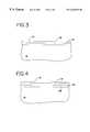
- silicon nitride layer 30is formed to overlie first silicon oxide layer 28 , as illustrated in FIG. 3 .
- silicon nitride layer 30is formed by means of a rapid-thermal-chemical-vapor-deposition (RTCVD) process.
- the RTCVD processis carried out at a temperature of about 700 to about 800° C.
- the silicon nitride materialis formed by reacting ammonia (NH 3 ) with either dichlorosilane (SiCl 2 H 2 ) or silane (SiH 4 ).
- silicon nitride layer 30can be deposited by other processes, such as a low-pressure-chemical-vapor-deposition (LPCVD) process, a selective deposition process, a molecular beam deposition process, a high-density-plasma (HDP) deposition process, and the like.
- LPCVDlow-pressure-chemical-vapor-deposition
- HDPhigh-density-plasma
- second silicon oxide layer 32is formed to overlie silicon nitride layer 30 , as illustrated in FIG. 4 .
- Second silicon oxide layer 32is formed by means of a steam oxidation process. Those skilled in the art will appreciate that the second silicon oxide layer 32 can be formed using a rapid-thermal-chemical-vapor-deposition (RTCVD) process. Second silicon oxide layer 32 is formed in an RTCVD apparatus using nitrous oxide (N 2 O) and dichlorosilane. The RTCVD processes preferably carried out at a temperature of about 700 to about 800° C.
- control-gate electrode 24is formed with polycrystalline silicon, amphorous silicon, a refractory metal silicide, and the like.
Landscapes
- Non-Volatile Memory (AREA)
- Semiconductor Memories (AREA)
Abstract
Description
Claims (20)
Priority Applications (1)
| Application Number | Priority Date | Filing Date | Title |
|---|---|---|---|
| US09/426,430US6248628B1 (en) | 1999-10-25 | 1999-10-25 | Method of fabricating an ONO dielectric by nitridation for MNOS memory cells |
Applications Claiming Priority (1)
| Application Number | Priority Date | Filing Date | Title |
|---|---|---|---|
| US09/426,430US6248628B1 (en) | 1999-10-25 | 1999-10-25 | Method of fabricating an ONO dielectric by nitridation for MNOS memory cells |
Publications (1)
| Publication Number | Publication Date |
|---|---|
| US6248628B1true US6248628B1 (en) | 2001-06-19 |
Family
ID=23690772
Family Applications (1)
| Application Number | Title | Priority Date | Filing Date |
|---|---|---|---|
| US09/426,430Expired - LifetimeUS6248628B1 (en) | 1999-10-25 | 1999-10-25 | Method of fabricating an ONO dielectric by nitridation for MNOS memory cells |
Country Status (1)
| Country | Link |
|---|---|
| US (1) | US6248628B1 (en) |
Cited By (38)
| Publication number | Priority date | Publication date | Assignee | Title |
|---|---|---|---|---|
| US6344394B1 (en)* | 1999-06-03 | 2002-02-05 | Mitsubishi Denki Kabushiki Kaisha | Method of manufacturing a semiconductor memory device having a capacitor with improved dielectric layer |
| US6395654B1 (en)* | 2000-08-25 | 2002-05-28 | Advanced Micro Devices, Inc. | Method of forming ONO flash memory devices using rapid thermal oxidation |
| US6406960B1 (en)* | 1999-10-25 | 2002-06-18 | Advanced Micro Devices, Inc. | Process for fabricating an ONO structure having a silicon-rich silicon nitride layer |
| US20020105023A1 (en)* | 2001-02-02 | 2002-08-08 | Kuo Tung Chen | Nov-volatile semiconductor memory cell utilizing poly-edge discharge |
| US6492677B2 (en)* | 2000-11-17 | 2002-12-10 | Fujitsu Limited | Non-volatile semiconductor memory device and fabrication process thereof |
| US20030017715A1 (en)* | 2001-02-01 | 2003-01-23 | Muller David A. | Composite gate dielectric layer |
| US6632747B2 (en)* | 2001-06-20 | 2003-10-14 | Texas Instruments Incorporated | Method of ammonia annealing of ultra-thin silicon dioxide layers for uniform nitrogen profile |
| US20030201491A1 (en)* | 1998-12-17 | 2003-10-30 | Samsung Electronics Co., Ltd. | Semiconductor device containing oxide/nitride/oxide dielectric layer and method of forming the same |
| US6660664B1 (en)* | 2000-03-31 | 2003-12-09 | International Business Machines Corp. | Structure and method for formation of a blocked silicide resistor |
| US20040002226A1 (en)* | 2002-07-01 | 2004-01-01 | International Business Machines Corporation | Method for fabricating a nitrided silicon-oxide gate dielectric |
| US6674138B1 (en) | 2001-12-31 | 2004-01-06 | Advanced Micro Devices, Inc. | Use of high-k dielectric materials in modified ONO structure for semiconductor devices |
| US20040049762A1 (en)* | 2002-09-09 | 2004-03-11 | Macronix International Co., Ltd. | Method for monitoring matched machine overlay |
| US20040046218A1 (en)* | 2002-09-10 | 2004-03-11 | Macronix International Co., Ltd. | Ono interpoly dielectric for flash memory cells and method for fabricating the same using a single wafer low temperature deposition process |
| US6750157B1 (en)* | 2000-10-12 | 2004-06-15 | Advanced Micro Devices, Inc. | Nonvolatile memory cell with a nitridated oxide layer |
| US20040166695A1 (en)* | 2002-09-19 | 2004-08-26 | Applied Materials, Inc. | Limited thermal budget formation of PMD layers |
| US20040185647A1 (en)* | 2002-02-08 | 2004-09-23 | Zhong Dong | Floating gate nitridation |
| US20050067663A1 (en)* | 2003-09-26 | 2005-03-31 | Krishnaswamy Ramkumar | Oxide-nitride stack gate dielectric |
| US20050101065A1 (en)* | 2003-10-01 | 2005-05-12 | Susumu Inoue | Method of manufacturing a semiconductor device |
| US20050255667A1 (en)* | 2004-05-14 | 2005-11-17 | Applied Materials, Inc., A Delaware Corporation | Method of inducing stresses in the channel region of a transistor |
| US20060030165A1 (en)* | 2004-08-04 | 2006-02-09 | Applied Materials, Inc. A Delaware Corporation | Multi-step anneal of thin films for film densification and improved gap-fill |
| US7053445B1 (en)* | 2005-08-02 | 2006-05-30 | Spansion Llc | Memory device with barrier layer |
| US7074677B1 (en)* | 2002-11-29 | 2006-07-11 | Fasl Llc | Memory with improved charge-trapping dielectric layer |
| US7115469B1 (en) | 2001-12-17 | 2006-10-03 | Spansion, Llc | Integrated ONO processing for semiconductor devices using in-situ steam generation (ISSG) process |
| US7141483B2 (en) | 2002-09-19 | 2006-11-28 | Applied Materials, Inc. | Nitrous oxide anneal of TEOS/ozone CVD for improved gapfill |
| US20070166923A1 (en)* | 2006-01-18 | 2007-07-19 | Macronix International Co., Ltd. | Method for nitridation of the interface between a dielectric and a substrate in a MOS device |
| US20070212847A1 (en)* | 2004-08-04 | 2007-09-13 | Applied Materials, Inc. | Multi-step anneal of thin films for film densification and improved gap-fill |
| US20070212850A1 (en)* | 2002-09-19 | 2007-09-13 | Applied Materials, Inc. | Gap-fill depositions in the formation of silicon containing dielectric materials |
| US20070215932A1 (en)* | 2006-03-20 | 2007-09-20 | Spansion Llc | Memory cell system using silicon-rich nitride |
| US20070231757A1 (en)* | 2006-03-29 | 2007-10-04 | Tokyo Electron Limited | Thermal processing furnace, gas delivery system therefor, and methods for delivering a process gas thereto |
| US20070238313A1 (en)* | 2006-03-30 | 2007-10-11 | Tokyo Electron Limited | Method for replacing a nitrous oxide based oxidation process with a nitric oxide based oxidation process for substrate processing |
| US20080115726A1 (en)* | 2004-08-27 | 2008-05-22 | Applied Materials, Inc. | gap-fill depositions introducing hydroxyl-containing precursors in the formation of silicon containing dielectric materials |
| US20080242109A1 (en)* | 2007-03-30 | 2008-10-02 | Tokyo Electron Limited | Method for growing a thin oxynitride film on a substrate |
| US7456116B2 (en) | 2002-09-19 | 2008-11-25 | Applied Materials, Inc. | Gap-fill depositions in the formation of silicon containing dielectric materials |
| US20090035463A1 (en)* | 2007-08-03 | 2009-02-05 | Tokyo Electron Limited | Thermal processing system and method for forming an oxide layer on substrates |
| US20090088000A1 (en)* | 2007-09-30 | 2009-04-02 | Tokyo Electron Limited | Method for growing an oxynitride film on a substrate |
| US20100155815A1 (en)* | 2008-12-23 | 2010-06-24 | Texas Instruments Incorporated | Ammonia pre-treatment in the fabrication of a memory cell |
| US8228725B2 (en)* | 2002-07-08 | 2012-07-24 | Micron Technology, Inc. | Memory utilizing oxide nanolaminates |
| US9018108B2 (en) | 2013-01-25 | 2015-04-28 | Applied Materials, Inc. | Low shrinkage dielectric films |
Citations (9)
| Publication number | Priority date | Publication date | Assignee | Title |
|---|---|---|---|---|
| US5407870A (en)* | 1993-06-07 | 1995-04-18 | Motorola Inc. | Process for fabricating a semiconductor device having a high reliability dielectric material |
| US5464792A (en)* | 1993-06-07 | 1995-11-07 | Motorola, Inc. | Process to incorporate nitrogen at an interface of a dielectric layer in a semiconductor device |
| US5712208A (en)* | 1994-06-09 | 1998-01-27 | Motorola, Inc. | Methods of formation of semiconductor composite gate dielectric having multiple incorporated atomic dopants |
| US5880498A (en)* | 1996-07-17 | 1999-03-09 | Kabushiki Kaisha Toshiba | Semiconductor device having a nitrogen doped polysilicon layer |
| US5939763A (en)* | 1996-09-05 | 1999-08-17 | Advanced Micro Devices, Inc. | Ultrathin oxynitride structure and process for VLSI applications |
| US5972804A (en)* | 1997-08-05 | 1999-10-26 | Motorola, Inc. | Process for forming a semiconductor device |
| US5981404A (en)* | 1996-11-22 | 1999-11-09 | United Microelectronics Corp. | Multilayer ONO structure |
| US6063666A (en)* | 1998-06-16 | 2000-05-16 | Advanced Micro Devices, Inc. | RTCVD oxide and N2 O anneal for top oxide of ONO film |
| US6117730A (en)* | 1999-10-25 | 2000-09-12 | Advanced Micro Devices, Inc. | Integrated method by using high temperature oxide for top oxide and periphery gate oxide |
- 1999
- 1999-10-25USUS09/426,430patent/US6248628B1/ennot_activeExpired - Lifetime
Patent Citations (9)
| Publication number | Priority date | Publication date | Assignee | Title |
|---|---|---|---|---|
| US5407870A (en)* | 1993-06-07 | 1995-04-18 | Motorola Inc. | Process for fabricating a semiconductor device having a high reliability dielectric material |
| US5464792A (en)* | 1993-06-07 | 1995-11-07 | Motorola, Inc. | Process to incorporate nitrogen at an interface of a dielectric layer in a semiconductor device |
| US5712208A (en)* | 1994-06-09 | 1998-01-27 | Motorola, Inc. | Methods of formation of semiconductor composite gate dielectric having multiple incorporated atomic dopants |
| US5880498A (en)* | 1996-07-17 | 1999-03-09 | Kabushiki Kaisha Toshiba | Semiconductor device having a nitrogen doped polysilicon layer |
| US5939763A (en)* | 1996-09-05 | 1999-08-17 | Advanced Micro Devices, Inc. | Ultrathin oxynitride structure and process for VLSI applications |
| US5981404A (en)* | 1996-11-22 | 1999-11-09 | United Microelectronics Corp. | Multilayer ONO structure |
| US5972804A (en)* | 1997-08-05 | 1999-10-26 | Motorola, Inc. | Process for forming a semiconductor device |
| US6063666A (en)* | 1998-06-16 | 2000-05-16 | Advanced Micro Devices, Inc. | RTCVD oxide and N2 O anneal for top oxide of ONO film |
| US6117730A (en)* | 1999-10-25 | 2000-09-12 | Advanced Micro Devices, Inc. | Integrated method by using high temperature oxide for top oxide and periphery gate oxide |
Cited By (68)
| Publication number | Priority date | Publication date | Assignee | Title |
|---|---|---|---|---|
| US20030201491A1 (en)* | 1998-12-17 | 2003-10-30 | Samsung Electronics Co., Ltd. | Semiconductor device containing oxide/nitride/oxide dielectric layer and method of forming the same |
| US6914013B2 (en)* | 1998-12-17 | 2005-07-05 | Samsung Electronics Co., Ltd. | Method of forming semiconductor device containing oxide/nitride/oxide dielectric layer |
| US6344394B1 (en)* | 1999-06-03 | 2002-02-05 | Mitsubishi Denki Kabushiki Kaisha | Method of manufacturing a semiconductor memory device having a capacitor with improved dielectric layer |
| US6605503B2 (en) | 1999-06-03 | 2003-08-12 | Mitsubishi Denki Kabushiki Kaisha | Method of manufacturing a semiconductor memory device having a capacitor with improved dielectric layer |
| US6448189B1 (en) | 1999-06-03 | 2002-09-10 | Mitsubishi Denki Kabushiki Kaisha | Method of manufacturing a semiconductor memory device having a capacitor with improved dielectric layer |
| US6406960B1 (en)* | 1999-10-25 | 2002-06-18 | Advanced Micro Devices, Inc. | Process for fabricating an ONO structure having a silicon-rich silicon nitride layer |
| US6853032B2 (en) | 2000-03-31 | 2005-02-08 | International Business Machines Corporation | Structure and method for formation of a blocked silicide resistor |
| US6660664B1 (en)* | 2000-03-31 | 2003-12-09 | International Business Machines Corp. | Structure and method for formation of a blocked silicide resistor |
| US20050095787A1 (en)* | 2000-03-31 | 2005-05-05 | International Business Machines Corporation | Structure and method for formation of a bipolar resistor |
| US6395654B1 (en)* | 2000-08-25 | 2002-05-28 | Advanced Micro Devices, Inc. | Method of forming ONO flash memory devices using rapid thermal oxidation |
| US6750157B1 (en)* | 2000-10-12 | 2004-06-15 | Advanced Micro Devices, Inc. | Nonvolatile memory cell with a nitridated oxide layer |
| US6492677B2 (en)* | 2000-11-17 | 2002-12-10 | Fujitsu Limited | Non-volatile semiconductor memory device and fabrication process thereof |
| US20030017715A1 (en)* | 2001-02-01 | 2003-01-23 | Muller David A. | Composite gate dielectric layer |
| US7253063B2 (en)* | 2001-02-01 | 2007-08-07 | Lucent Technologies Inc. | Method of fabricating a composite gate dielectric layer |
| US20020105023A1 (en)* | 2001-02-02 | 2002-08-08 | Kuo Tung Chen | Nov-volatile semiconductor memory cell utilizing poly-edge discharge |
| US6894340B2 (en)* | 2001-02-02 | 2005-05-17 | Macronix International | Non-volatile semiconductor memory cell utilizing poly-edge discharge |
| US6632747B2 (en)* | 2001-06-20 | 2003-10-14 | Texas Instruments Incorporated | Method of ammonia annealing of ultra-thin silicon dioxide layers for uniform nitrogen profile |
| US7115469B1 (en) | 2001-12-17 | 2006-10-03 | Spansion, Llc | Integrated ONO processing for semiconductor devices using in-situ steam generation (ISSG) process |
| US6803272B1 (en) | 2001-12-31 | 2004-10-12 | Advanced Micro Devices, Inc. | Use of high-K dielectric material in modified ONO structure for semiconductor devices |
| US6674138B1 (en) | 2001-12-31 | 2004-01-06 | Advanced Micro Devices, Inc. | Use of high-k dielectric materials in modified ONO structure for semiconductor devices |
| US7001810B2 (en) | 2002-02-08 | 2006-02-21 | Promos Technologies Inc. | Floating gate nitridation |
| US20040185647A1 (en)* | 2002-02-08 | 2004-09-23 | Zhong Dong | Floating gate nitridation |
| US6780720B2 (en) | 2002-07-01 | 2004-08-24 | International Business Machines Corporation | Method for fabricating a nitrided silicon-oxide gate dielectric |
| US20040002226A1 (en)* | 2002-07-01 | 2004-01-01 | International Business Machines Corporation | Method for fabricating a nitrided silicon-oxide gate dielectric |
| US8228725B2 (en)* | 2002-07-08 | 2012-07-24 | Micron Technology, Inc. | Memory utilizing oxide nanolaminates |
| US20040049762A1 (en)* | 2002-09-09 | 2004-03-11 | Macronix International Co., Ltd. | Method for monitoring matched machine overlay |
| US6777764B2 (en)* | 2002-09-10 | 2004-08-17 | Macronix International Co., Ltd. | ONO interpoly dielectric for flash memory cells and method for fabricating the same using a single wafer low temperature deposition process |
| US20040046218A1 (en)* | 2002-09-10 | 2004-03-11 | Macronix International Co., Ltd. | Ono interpoly dielectric for flash memory cells and method for fabricating the same using a single wafer low temperature deposition process |
| US7674727B2 (en) | 2002-09-19 | 2010-03-09 | Applied Materials, Inc. | Nitrous oxide anneal of TEOS/ozone CVD for improved gapfill |
| US7456116B2 (en) | 2002-09-19 | 2008-11-25 | Applied Materials, Inc. | Gap-fill depositions in the formation of silicon containing dielectric materials |
| US20070059896A1 (en)* | 2002-09-19 | 2007-03-15 | Applied Materials, Inc. | Nitrous oxide anneal of teos/ozone cvd for improved gapfill |
| US20070212850A1 (en)* | 2002-09-19 | 2007-09-13 | Applied Materials, Inc. | Gap-fill depositions in the formation of silicon containing dielectric materials |
| US20040166695A1 (en)* | 2002-09-19 | 2004-08-26 | Applied Materials, Inc. | Limited thermal budget formation of PMD layers |
| US7141483B2 (en) | 2002-09-19 | 2006-11-28 | Applied Materials, Inc. | Nitrous oxide anneal of TEOS/ozone CVD for improved gapfill |
| US7431967B2 (en) | 2002-09-19 | 2008-10-07 | Applied Materials, Inc. | Limited thermal budget formation of PMD layers |
| US7074677B1 (en)* | 2002-11-29 | 2006-07-11 | Fasl Llc | Memory with improved charge-trapping dielectric layer |
| US8445381B2 (en) | 2003-09-26 | 2013-05-21 | Cypress Semiconductor Corporation | Oxide-nitride stack gate dielectric |
| US20050067663A1 (en)* | 2003-09-26 | 2005-03-31 | Krishnaswamy Ramkumar | Oxide-nitride stack gate dielectric |
| US20080093680A1 (en)* | 2003-09-26 | 2008-04-24 | Krishnaswamy Ramkumar | Oxide-nitride stack gate dielectric |
| US7371637B2 (en)* | 2003-09-26 | 2008-05-13 | Cypress Semiconductor Corporation | Oxide-nitride stack gate dielectric |
| US20050101065A1 (en)* | 2003-10-01 | 2005-05-12 | Susumu Inoue | Method of manufacturing a semiconductor device |
| US7528051B2 (en) | 2004-05-14 | 2009-05-05 | Applied Materials, Inc. | Method of inducing stresses in the channel region of a transistor |
| US20050255667A1 (en)* | 2004-05-14 | 2005-11-17 | Applied Materials, Inc., A Delaware Corporation | Method of inducing stresses in the channel region of a transistor |
| US20070000897A1 (en)* | 2004-08-04 | 2007-01-04 | Applied Materials, Inc. | Multi-step anneal of thin films for film densification and improved gap-fill |
| US7642171B2 (en) | 2004-08-04 | 2010-01-05 | Applied Materials, Inc. | Multi-step anneal of thin films for film densification and improved gap-fill |
| US20060030165A1 (en)* | 2004-08-04 | 2006-02-09 | Applied Materials, Inc. A Delaware Corporation | Multi-step anneal of thin films for film densification and improved gap-fill |
| US20070212847A1 (en)* | 2004-08-04 | 2007-09-13 | Applied Materials, Inc. | Multi-step anneal of thin films for film densification and improved gap-fill |
| US20080115726A1 (en)* | 2004-08-27 | 2008-05-22 | Applied Materials, Inc. | gap-fill depositions introducing hydroxyl-containing precursors in the formation of silicon containing dielectric materials |
| WO2007019027A1 (en) | 2005-08-02 | 2007-02-15 | Spansion Llc | Memory device with barrier layer |
| US20080191269A1 (en)* | 2005-08-02 | 2008-08-14 | Spansion Llc | Memory Device with Barrier Layer |
| US7816724B2 (en) | 2005-08-02 | 2010-10-19 | Spansion Llc | Memory device with barrier layer |
| US7053445B1 (en)* | 2005-08-02 | 2006-05-30 | Spansion Llc | Memory device with barrier layer |
| US7824991B2 (en)* | 2006-01-18 | 2010-11-02 | Macronix International Co., Ltd. | Method for nitridation of the interface between a dielectric and a substrate in a MOS device |
| US20070166923A1 (en)* | 2006-01-18 | 2007-07-19 | Macronix International Co., Ltd. | Method for nitridation of the interface between a dielectric and a substrate in a MOS device |
| US20070215932A1 (en)* | 2006-03-20 | 2007-09-20 | Spansion Llc | Memory cell system using silicon-rich nitride |
| US8803216B2 (en)* | 2006-03-20 | 2014-08-12 | Spansion, Llc | Memory cell system using silicon-rich nitride |
| US7910494B2 (en) | 2006-03-29 | 2011-03-22 | Tokyo Electron Limited | Thermal processing furnace, gas delivery system therefor, and methods for delivering a process gas thereto |
| US20070231757A1 (en)* | 2006-03-29 | 2007-10-04 | Tokyo Electron Limited | Thermal processing furnace, gas delivery system therefor, and methods for delivering a process gas thereto |
| US7635655B2 (en) | 2006-03-30 | 2009-12-22 | Tokyo Electron Limited | Method for replacing a nitrous oxide based oxidation process with a nitric oxide based oxidation process for substrate processing |
| US20070238313A1 (en)* | 2006-03-30 | 2007-10-11 | Tokyo Electron Limited | Method for replacing a nitrous oxide based oxidation process with a nitric oxide based oxidation process for substrate processing |
| US7534731B2 (en) | 2007-03-30 | 2009-05-19 | Tokyo Electron Limited | Method for growing a thin oxynitride film on a substrate |
| US20080242109A1 (en)* | 2007-03-30 | 2008-10-02 | Tokyo Electron Limited | Method for growing a thin oxynitride film on a substrate |
| US20090035463A1 (en)* | 2007-08-03 | 2009-02-05 | Tokyo Electron Limited | Thermal processing system and method for forming an oxide layer on substrates |
| US20090088000A1 (en)* | 2007-09-30 | 2009-04-02 | Tokyo Electron Limited | Method for growing an oxynitride film on a substrate |
| US7659214B2 (en) | 2007-09-30 | 2010-02-09 | Tokyo Electron Limited | Method for growing an oxynitride film on a substrate |
| US8283224B2 (en)* | 2008-12-23 | 2012-10-09 | Texas Instruments Incorporated | Ammonia pre-treatment in the fabrication of a memory cell |
| US20100155815A1 (en)* | 2008-12-23 | 2010-06-24 | Texas Instruments Incorporated | Ammonia pre-treatment in the fabrication of a memory cell |
| US9018108B2 (en) | 2013-01-25 | 2015-04-28 | Applied Materials, Inc. | Low shrinkage dielectric films |
Similar Documents
| Publication | Publication Date | Title |
|---|---|---|
| US6248628B1 (en) | Method of fabricating an ONO dielectric by nitridation for MNOS memory cells | |
| US6406960B1 (en) | Process for fabricating an ONO structure having a silicon-rich silicon nitride layer | |
| US6265268B1 (en) | High temperature oxide deposition process for fabricating an ONO floating-gate electrode in a two bit EEPROM device | |
| US6319775B1 (en) | Nitridation process for fabricating an ONO floating-gate electrode in a two-bit EEPROM device | |
| US6458677B1 (en) | Process for fabricating an ONO structure | |
| US7115469B1 (en) | Integrated ONO processing for semiconductor devices using in-situ steam generation (ISSG) process | |
| KR101017713B1 (en) | Charge-Trap Memory Array Prevents Damage Due to Contact Hole Formation | |
| US6458656B1 (en) | Process for creating a flash memory cell using a photoresist flow operation | |
| US6903968B2 (en) | Nonvolatile memory capable of storing multibits binary information and the method of forming the same | |
| US6445030B1 (en) | Flash memory erase speed by fluorine implant or fluorination | |
| US5585293A (en) | Fabrication process for a 1-transistor EEPROM memory device capable of low-voltage operation | |
| US6261904B1 (en) | Dual bit isolation scheme for flash devices | |
| US6127227A (en) | Thin ONO thickness control and gradual gate oxidation suppression by b. N.su2 treatment in flash memory | |
| US6180538B1 (en) | Process for fabricating an ONO floating-gate electrode in a two-bit EEPROM device using rapid-thermal-chemical-vapor-deposition | |
| US6753569B2 (en) | Method to fabricate a non-smiling effect structure in split-gate flash with self-aligned isolation | |
| US6252276B1 (en) | Non-volatile semiconductor memory device including assymetrically nitrogen doped gate oxide | |
| US6188103B1 (en) | Method of forming sharp beak of poly by nitrogen implant to improve erase speed for split-gate flash | |
| US7442989B2 (en) | Nonvolatile semiconductor memory device and method of manufacturing thereof | |
| US6326660B1 (en) | Method to improve the capacity of data retention and increase the coupling ratio of source to floating gate in split-gate flash | |
| US6465841B1 (en) | Split gate flash memory device having nitride spacer to prevent inter-poly oxide damage | |
| US6218227B1 (en) | Method to generate a MONOS type flash cell using polycrystalline silicon as an ONO top layer | |
| JP2002009179A (en) | Nonvolatile semiconductor memory device and method of manufacturing the same | |
| JP2002261175A (en) | Nonvolatile semiconductor memory and its manufacturing method | |
| US7033956B1 (en) | Semiconductor memory devices and methods for making the same | |
| JP4969748B2 (en) | Nonvolatile semiconductor memory device and method of manufacturing nonvolatile memory cell |
Legal Events
| Date | Code | Title | Description |
|---|---|---|---|
| AS | Assignment | Owner name:ADVANCED MICRO DEVICES, INC., CALIFORNIA Free format text:ASSIGNMENT OF ASSIGNORS INTEREST;ASSIGNORS:HALLIYAL, ARVIND;FOOTE, DAVID K.;KOMORI, HIDEKI;AND OTHERS;REEL/FRAME:010616/0083;SIGNING DATES FROM 20000112 TO 20000201 Owner name:FUJITSU LIMITED, JAPAN Free format text:ASSIGNMENT OF ASSIGNORS INTEREST;ASSIGNORS:HALLIYAL, ARVIND;FOOTE, DAVID K.;KOMORI, HIDEKI;AND OTHERS;REEL/FRAME:010616/0083;SIGNING DATES FROM 20000112 TO 20000201 | |
| STCF | Information on status: patent grant | Free format text:PATENTED CASE | |
| CC | Certificate of correction | ||
| CC | Certificate of correction | ||
| AS | Assignment | Owner name:AMD HOLDINGS, INC., CALIFORNIA Free format text:ASSIGNMENT OF ASSIGNORS INTEREST;ASSIGNOR:ADVANCED MICRO DEVICES, INC.;REEL/FRAME:015452/0593 Effective date:20040330 | |
| AS | Assignment | Owner name:AMD INVESTMENTS, INC., CALIFORNIA Free format text:ASSIGNMENT OF ASSIGNORS INTEREST;ASSIGNOR:AMD HOLDINGS, INC.;REEL/FRAME:015478/0820 Effective date:20040330 Owner name:FASL, LLC, CALIFORNIA Free format text:ASSIGNMENT OF ASSIGNORS INTEREST;ASSIGNORS:AMD INVESTMENTS, INC.;FUJITSU LIMITED;REEL/FRAME:014754/0749;SIGNING DATES FROM 20040330 TO 20040514 | |
| FPAY | Fee payment | Year of fee payment:4 | |
| FPAY | Fee payment | Year of fee payment:8 | |
| AS | Assignment | Owner name:SPANSION LLC,CALIFORNIA Free format text:CHANGE OF NAME;ASSIGNOR:FASL LLC;REEL/FRAME:024170/0300 Effective date:20100401 | |
| AS | Assignment | Owner name:BARCLAYS BANK PLC,NEW YORK Free format text:SECURITY AGREEMENT;ASSIGNORS:SPANSION LLC;SPANSION INC.;SPANSION TECHNOLOGY INC.;AND OTHERS;REEL/FRAME:024522/0338 Effective date:20100510 Owner name:BARCLAYS BANK PLC, NEW YORK Free format text:SECURITY AGREEMENT;ASSIGNORS:SPANSION LLC;SPANSION INC.;SPANSION TECHNOLOGY INC.;AND OTHERS;REEL/FRAME:024522/0338 Effective date:20100510 | |
| FPAY | Fee payment | Year of fee payment:12 | |
| AS | Assignment | Owner name:SPANSION LLC, CALIFORNIA Free format text:RELEASE BY SECURED PARTY;ASSIGNOR:BARCLAYS BANK PLC;REEL/FRAME:035201/0159 Effective date:20150312 Owner name:SPANSION INC., CALIFORNIA Free format text:RELEASE BY SECURED PARTY;ASSIGNOR:BARCLAYS BANK PLC;REEL/FRAME:035201/0159 Effective date:20150312 Owner name:SPANSION TECHNOLOGY LLC, CALIFORNIA Free format text:RELEASE BY SECURED PARTY;ASSIGNOR:BARCLAYS BANK PLC;REEL/FRAME:035201/0159 Effective date:20150312 | |
| AS | Assignment | Owner name:MORGAN STANLEY SENIOR FUNDING, INC., NEW YORK Free format text:SECURITY INTEREST;ASSIGNORS:CYPRESS SEMICONDUCTOR CORPORATION;SPANSION LLC;REEL/FRAME:035240/0429 Effective date:20150312 | |
| AS | Assignment | Owner name:CYPRESS SEMICONDUCTOR CORPORATION, CALIFORNIA Free format text:ASSIGNMENT OF ASSIGNORS INTEREST;ASSIGNOR:SPANSION, LLC;REEL/FRAME:036030/0001 Effective date:20150601 | |
| AS | Assignment | Owner name:CYPRESS SEMICONDUCTOR CORPORATION, CALIFORNIA Free format text:PARTIAL RELEASE OF SECURITY INTEREST IN PATENTS;ASSIGNOR:MORGAN STANLEY SENIOR FUNDING, INC., AS COLLATERAL AGENT;REEL/FRAME:039708/0001 Effective date:20160811 Owner name:SPANSION LLC, CALIFORNIA Free format text:PARTIAL RELEASE OF SECURITY INTEREST IN PATENTS;ASSIGNOR:MORGAN STANLEY SENIOR FUNDING, INC., AS COLLATERAL AGENT;REEL/FRAME:039708/0001 Effective date:20160811 | |
| AS | Assignment | Owner name:MONTEREY RESEARCH, LLC, CALIFORNIA Free format text:ASSIGNMENT OF ASSIGNORS INTEREST;ASSIGNOR:CYPRESS SEMICONDUCTOR CORPORATION;REEL/FRAME:040911/0238 Effective date:20160811 | |
| AS | Assignment | Owner name:MORGAN STANLEY SENIOR FUNDING, INC., NEW YORK Free format text:CORRECTIVE ASSIGNMENT TO CORRECT THE 8647899 PREVIOUSLY RECORDED ON REEL 035240 FRAME 0429. ASSIGNOR(S) HEREBY CONFIRMS THE SECURITY INTERST;ASSIGNORS:CYPRESS SEMICONDUCTOR CORPORATION;SPANSION LLC;REEL/FRAME:058002/0470 Effective date:20150312 |