US6247635B1 - High density connector having a ball type of contact surface - Google Patents
High density connector having a ball type of contact surfaceDownload PDFInfo
- Publication number
- US6247635B1 US6247635B1US09/564,760US56476000AUS6247635B1US 6247635 B1US6247635 B1US 6247635B1US 56476000 AUS56476000 AUS 56476000AUS 6247635 B1US6247635 B1US 6247635B1
- Authority
- US
- United States
- Prior art keywords
- opening
- tail
- housing
- connector
- solder
- Prior art date
- Legal status (The legal status is an assumption and is not a legal conclusion. Google has not performed a legal analysis and makes no representation as to the accuracy of the status listed.)
- Expired - Lifetime
Links
Images


Classifications
- H—ELECTRICITY
- H01—ELECTRIC ELEMENTS
- H01R—ELECTRICALLY-CONDUCTIVE CONNECTIONS; STRUCTURAL ASSOCIATIONS OF A PLURALITY OF MUTUALLY-INSULATED ELECTRICAL CONNECTING ELEMENTS; COUPLING DEVICES; CURRENT COLLECTORS
- H01R12/00—Structural associations of a plurality of mutually-insulated electrical connecting elements, specially adapted for printed circuits, e.g. printed circuit boards [PCB], flat or ribbon cables, or like generally planar structures, e.g. terminal strips, terminal blocks; Coupling devices specially adapted for printed circuits, flat or ribbon cables, or like generally planar structures; Terminals specially adapted for contact with, or insertion into, printed circuits, flat or ribbon cables, or like generally planar structures
- H01R12/70—Coupling devices
- H01R12/71—Coupling devices for rigid printing circuits or like structures
- H—ELECTRICITY
- H01—ELECTRIC ELEMENTS
- H01R—ELECTRICALLY-CONDUCTIVE CONNECTIONS; STRUCTURAL ASSOCIATIONS OF A PLURALITY OF MUTUALLY-INSULATED ELECTRICAL CONNECTING ELEMENTS; COUPLING DEVICES; CURRENT COLLECTORS
- H01R12/00—Structural associations of a plurality of mutually-insulated electrical connecting elements, specially adapted for printed circuits, e.g. printed circuit boards [PCB], flat or ribbon cables, or like generally planar structures, e.g. terminal strips, terminal blocks; Coupling devices specially adapted for printed circuits, flat or ribbon cables, or like generally planar structures; Terminals specially adapted for contact with, or insertion into, printed circuits, flat or ribbon cables, or like generally planar structures
- H01R12/50—Fixed connections
- H01R12/51—Fixed connections for rigid printed circuits or like structures
- H01R12/55—Fixed connections for rigid printed circuits or like structures characterised by the terminals
- H01R12/57—Fixed connections for rigid printed circuits or like structures characterised by the terminals surface mounting terminals
- H—ELECTRICITY
- H01—ELECTRIC ELEMENTS
- H01R—ELECTRICALLY-CONDUCTIVE CONNECTIONS; STRUCTURAL ASSOCIATIONS OF A PLURALITY OF MUTUALLY-INSULATED ELECTRICAL CONNECTING ELEMENTS; COUPLING DEVICES; CURRENT COLLECTORS
- H01R12/00—Structural associations of a plurality of mutually-insulated electrical connecting elements, specially adapted for printed circuits, e.g. printed circuit boards [PCB], flat or ribbon cables, or like generally planar structures, e.g. terminal strips, terminal blocks; Coupling devices specially adapted for printed circuits, flat or ribbon cables, or like generally planar structures; Terminals specially adapted for contact with, or insertion into, printed circuits, flat or ribbon cables, or like generally planar structures
- H01R12/70—Coupling devices
- H01R12/71—Coupling devices for rigid printing circuits or like structures
- H01R12/72—Coupling devices for rigid printing circuits or like structures coupling with the edge of the rigid printed circuits or like structures
- H01R12/721—Coupling devices for rigid printing circuits or like structures coupling with the edge of the rigid printed circuits or like structures cooperating directly with the edge of the rigid printed circuits
- H—ELECTRICITY
- H05—ELECTRIC TECHNIQUES NOT OTHERWISE PROVIDED FOR
- H05K—PRINTED CIRCUITS; CASINGS OR CONSTRUCTIONAL DETAILS OF ELECTRIC APPARATUS; MANUFACTURE OF ASSEMBLAGES OF ELECTRICAL COMPONENTS
- H05K3/00—Apparatus or processes for manufacturing printed circuits
- H05K3/30—Assembling printed circuits with electric components, e.g. with resistor
- H05K3/32—Assembling printed circuits with electric components, e.g. with resistor electrically connecting electric components or wires to printed circuits
- H05K3/34—Assembling printed circuits with electric components, e.g. with resistor electrically connecting electric components or wires to printed circuits by soldering
- H05K3/341—Surface mounted components
- H05K3/3431—Leadless components
- H05K3/3436—Leadless components having an array of bottom contacts, e.g. pad grid array or ball grid array components
- H—ELECTRICITY
- H01—ELECTRIC ELEMENTS
- H01R—ELECTRICALLY-CONDUCTIVE CONNECTIONS; STRUCTURAL ASSOCIATIONS OF A PLURALITY OF MUTUALLY-INSULATED ELECTRICAL CONNECTING ELEMENTS; COUPLING DEVICES; CURRENT COLLECTORS
- H01R12/00—Structural associations of a plurality of mutually-insulated electrical connecting elements, specially adapted for printed circuits, e.g. printed circuit boards [PCB], flat or ribbon cables, or like generally planar structures, e.g. terminal strips, terminal blocks; Coupling devices specially adapted for printed circuits, flat or ribbon cables, or like generally planar structures; Terminals specially adapted for contact with, or insertion into, printed circuits, flat or ribbon cables, or like generally planar structures
- H01R12/70—Coupling devices
- H01R12/71—Coupling devices for rigid printing circuits or like structures
- H01R12/72—Coupling devices for rigid printing circuits or like structures coupling with the edge of the rigid printed circuits or like structures
- H01R12/722—Coupling devices for rigid printing circuits or like structures coupling with the edge of the rigid printed circuits or like structures coupling devices mounted on the edge of the printed circuits
- H01R12/725—Coupling devices for rigid printing circuits or like structures coupling with the edge of the rigid printed circuits or like structures coupling devices mounted on the edge of the printed circuits containing contact members presenting a contact carrying strip, e.g. edge-like strip
- H—ELECTRICITY
- H01—ELECTRIC ELEMENTS
- H01R—ELECTRICALLY-CONDUCTIVE CONNECTIONS; STRUCTURAL ASSOCIATIONS OF A PLURALITY OF MUTUALLY-INSULATED ELECTRICAL CONNECTING ELEMENTS; COUPLING DEVICES; CURRENT COLLECTORS
- H01R13/00—Details of coupling devices of the kinds covered by groups H01R12/70 or H01R24/00 - H01R33/00
- H01R13/46—Bases; Cases
- H01R13/516—Means for holding or embracing insulating body, e.g. casing, hoods
- H01R13/518—Means for holding or embracing insulating body, e.g. casing, hoods for holding or embracing several coupling parts, e.g. frames
- H—ELECTRICITY
- H05—ELECTRIC TECHNIQUES NOT OTHERWISE PROVIDED FOR
- H05K—PRINTED CIRCUITS; CASINGS OR CONSTRUCTIONAL DETAILS OF ELECTRIC APPARATUS; MANUFACTURE OF ASSEMBLAGES OF ELECTRICAL COMPONENTS
- H05K2201/00—Indexing scheme relating to printed circuits covered by H05K1/00
- H05K2201/09—Shape and layout
- H05K2201/09009—Substrate related
- H05K2201/09036—Recesses or grooves in insulating substrate
- H—ELECTRICITY
- H05—ELECTRIC TECHNIQUES NOT OTHERWISE PROVIDED FOR
- H05K—PRINTED CIRCUITS; CASINGS OR CONSTRUCTIONAL DETAILS OF ELECTRIC APPARATUS; MANUFACTURE OF ASSEMBLAGES OF ELECTRICAL COMPONENTS
- H05K2201/00—Indexing scheme relating to printed circuits covered by H05K1/00
- H05K2201/10—Details of components or other objects attached to or integrated in a printed circuit board
- H05K2201/10007—Types of components
- H05K2201/10189—Non-printed connector
- H—ELECTRICITY
- H05—ELECTRIC TECHNIQUES NOT OTHERWISE PROVIDED FOR
- H05K—PRINTED CIRCUITS; CASINGS OR CONSTRUCTIONAL DETAILS OF ELECTRIC APPARATUS; MANUFACTURE OF ASSEMBLAGES OF ELECTRICAL COMPONENTS
- H05K2201/00—Indexing scheme relating to printed circuits covered by H05K1/00
- H05K2201/10—Details of components or other objects attached to or integrated in a printed circuit board
- H05K2201/10227—Other objects, e.g. metallic pieces
- H05K2201/10424—Frame holders
- H—ELECTRICITY
- H05—ELECTRIC TECHNIQUES NOT OTHERWISE PROVIDED FOR
- H05K—PRINTED CIRCUITS; CASINGS OR CONSTRUCTIONAL DETAILS OF ELECTRIC APPARATUS; MANUFACTURE OF ASSEMBLAGES OF ELECTRICAL COMPONENTS
- H05K2201/00—Indexing scheme relating to printed circuits covered by H05K1/00
- H05K2201/10—Details of components or other objects attached to or integrated in a printed circuit board
- H05K2201/10431—Details of mounted components
- H05K2201/10568—Integral adaptations of a component or an auxiliary PCB for mounting, e.g. integral spacer element
- H—ELECTRICITY
- H05—ELECTRIC TECHNIQUES NOT OTHERWISE PROVIDED FOR
- H05K—PRINTED CIRCUITS; CASINGS OR CONSTRUCTIONAL DETAILS OF ELECTRIC APPARATUS; MANUFACTURE OF ASSEMBLAGES OF ELECTRICAL COMPONENTS
- H05K2201/00—Indexing scheme relating to printed circuits covered by H05K1/00
- H05K2201/20—Details of printed circuits not provided for in H05K2201/01 - H05K2201/10
- H05K2201/2036—Permanent spacer or stand-off in a printed circuit or printed circuit assembly
- H—ELECTRICITY
- H05—ELECTRIC TECHNIQUES NOT OTHERWISE PROVIDED FOR
- H05K—PRINTED CIRCUITS; CASINGS OR CONSTRUCTIONAL DETAILS OF ELECTRIC APPARATUS; MANUFACTURE OF ASSEMBLAGES OF ELECTRICAL COMPONENTS
- H05K2203/00—Indexing scheme relating to apparatus or processes for manufacturing printed circuits covered by H05K3/00
- H05K2203/04—Soldering or other types of metallurgic bonding
- H05K2203/041—Solder preforms in the shape of solder balls
- H—ELECTRICITY
- H05—ELECTRIC TECHNIQUES NOT OTHERWISE PROVIDED FOR
- H05K—PRINTED CIRCUITS; CASINGS OR CONSTRUCTIONAL DETAILS OF ELECTRIC APPARATUS; MANUFACTURE OF ASSEMBLAGES OF ELECTRICAL COMPONENTS
- H05K3/00—Apparatus or processes for manufacturing printed circuits
- H05K3/30—Assembling printed circuits with electric components, e.g. with resistor
- H05K3/32—Assembling printed circuits with electric components, e.g. with resistor electrically connecting electric components or wires to printed circuits
- H05K3/34—Assembling printed circuits with electric components, e.g. with resistor electrically connecting electric components or wires to printed circuits by soldering
- H05K3/341—Surface mounted components
- H05K3/3421—Leaded components
- H05K3/3426—Leaded components characterised by the leads
- H—ELECTRICITY
- H05—ELECTRIC TECHNIQUES NOT OTHERWISE PROVIDED FOR
- H05K—PRINTED CIRCUITS; CASINGS OR CONSTRUCTIONAL DETAILS OF ELECTRIC APPARATUS; MANUFACTURE OF ASSEMBLAGES OF ELECTRICAL COMPONENTS
- H05K3/00—Apparatus or processes for manufacturing printed circuits
- H05K3/30—Assembling printed circuits with electric components, e.g. with resistor
- H05K3/32—Assembling printed circuits with electric components, e.g. with resistor electrically connecting electric components or wires to printed circuits
- H05K3/34—Assembling printed circuits with electric components, e.g. with resistor electrically connecting electric components or wires to printed circuits by soldering
- H05K3/3457—Solder materials or compositions; Methods of application thereof
- H05K3/3485—Applying solder paste, slurry or powder
- Y—GENERAL TAGGING OF NEW TECHNOLOGICAL DEVELOPMENTS; GENERAL TAGGING OF CROSS-SECTIONAL TECHNOLOGIES SPANNING OVER SEVERAL SECTIONS OF THE IPC; TECHNICAL SUBJECTS COVERED BY FORMER USPC CROSS-REFERENCE ART COLLECTIONS [XRACs] AND DIGESTS
- Y02—TECHNOLOGIES OR APPLICATIONS FOR MITIGATION OR ADAPTATION AGAINST CLIMATE CHANGE
- Y02P—CLIMATE CHANGE MITIGATION TECHNOLOGIES IN THE PRODUCTION OR PROCESSING OF GOODS
- Y02P70/00—Climate change mitigation technologies in the production process for final industrial or consumer products
- Y02P70/50—Manufacturing or production processes characterised by the final manufactured product
Definitions
- the present inventionrelates to electrical connectors and more particularly to high I/O density connectors such as connectors that are attachable to a circuit substrate by use of a solder ball contact surface.
- the drive to reduce the size of electronic equipment, particularly personal portable devices, and to add additional functions to such equipmenthas resulted in an ongoing drive for miniaturization of all components, especially electrical connectors.
- Efforts to miniaturize electrical connectorshave included reductions in the pitch between terminals in single or double row linear connectors, so that a relatively high number of I/O or other lines can be interconnected by connectors that fit within the tightly circumscribed areas on circuit substrates that are allotted for receiving connectors.
- the drive for miniaturizationhas also been accompanied by a shift in manufacturing preference to surface mount techniques (SMT) for mounting components on circuit substrates.
- SMTsurface mount techniques
- solder ballspherical solder balls attached to the IC package are positioned on electrical contact pads of a circuit substrate to which a layer of solder paste has been applied, typically by use of a screen or mask.
- the unitis then heated to a temperature at which the solder paste and at least a portion of the solder ball melt and fuse to an underlying conductive pad formed on the circuit substrate. This heating process is commonly referred to as solder reflow.
- solder reflowsolder reflow
- solder balls and similar systems in connecting ICs to a substratehas many advantages
- a corresponding means for mounting an electrical connector or similar component on a circuit substratehas recently become desirable.
- the use of such techniques in mounting electrical connectorshas lagged the use in mounting ICs because the use of solder ball technologies in mounting an electrical connector or similar component to a circuit substrate presents complexities not encountered with IC mounting.
- ICs that have employed solder ballsgenerally present a flat attachment surface.
- connectorsusually do not present a flat attachment surface but rather present a series of elongated conductors, commonly referred to as terminal tail ends. Attachment of a solder ball to the small end surface presented by the tip of a terminal tail end presents manufacturing difficulties not present in the attachment of solder balls to a flat surface.
- connectorsare generally more susceptible to solder joint stress due to the effects of differential Coefficients of Thermal Expansion (CTE) between the connector and the circuit substrate.
- CTEdifferential Coefficients of Thermal Expansion
- This susceptibilityis primarily due to size and geometry differences between a connector and an IC.
- IC mounting surfacesare generally on the order of 2.5 centimeters square.
- Connector mounting surfaceson the other hand, generally have a narrow width (e.g., 0.5 centimeters or less)and a much longer length (e.g. 5.0 centimeters or more).
- CTECoefficients of Thermal Expansion
- Connectors attached to circuit substrates via solder ball techniquesare also more susceptible to joint stress than a conventional SMT attachment technique.
- a conventional SMTattaches connector terminal tails to a circuit substrate horizontally, providing more attachment surface area for the solder joint.
- the additional surface area of the solder joint in the conventional SMT techniqueis stronger and, consequently, more tolerant of differences in CTE between the connector, terminal tails and circuit substrate.
- a solder ball connectionattaches a connector terminal tail vertically to the circuit substrate with the end of the terminal tail directly mated to the circuit substrate, reducing the amount of attachment surface area.
- differences in CTEare much more likely to stress the terminal tail to circuit substrate joint resulting in failure or quality problems.
- solder ballsto attach a connector to a circuit substrate imposes the requirement that the solder balls are coplanar in order to ensure a substantially flat mounting interface. So that, in the final application the balls will reflow and solder evenly to a planar circuit substrate. Any significant differences in solder coplanarity on a given mounting connection can cause poor soldering performance when the connector is reflowed onto a printed circuit board. Accordingly, users specify very tight coplanarity requirements to achieve high soldering reliability, on the order of 0.1 to 0.2 mm for example. By providing a connection using a solder ball technique, the coplanarity requirements can be met and sometimes exceeded. Unlike conventional SMT, the solder ball can absorb variations in terminal tail length by changing shape upon the application of heat to bridge the gaps between the terminal tail ends and the circuit substrate connections.
- the present inventionrecognizes that there is a need for an improved electrical connector apparatus and accompanying electrical connector construction techniques that address the shortcomings of present electrical connectors.
- the inventionmeets the above needs by providing an improved electrical connector for use in forming an electrical connection between a contact portion of an electrical component and a contact portion of a circuit substrate and method for constructing the electrical connector.
- the electrical connectorcomprises a connector body, a plurality of electrical contacts disposed on the connector body arranged to electrically mate with the contact portion of the electrical component, a plurality of electrical elongated conductors, alternately referred to as terminal tails, disposed on the connector body are arranged to form an electrical connection with the circuit substrate.
- the elongated conductorsare in electrical communication with corresponding electrical contacts.
- a substrate contactsuch as a solder ball, is connected via a butt joint on an end of each of the elongated conductors such that an electrical connection between the elongated conductors and the contact portion of the circuit substrate is selectively accommodated.
- Each of the elongated conductorsis disposed in a passage that has cross-sectional diameter a little larger than the cross-sectional diameter of the elongated conductor.
- the cross-sectionis substantially rectangular in shape.
- the passagesterminate in wells that are disposed across a planar face of the connector.
- the wellshave a rectangular top opening that is longer along a length of the connector face.
- a portion of the connector body proximate the elongated connector tail endis coated with an antimigration solution such as oleophobic-hydrophobic flourochemical polymer to assist the process of solder ball formation and attachment.
- One of the primary manufacturing challenges in manufacturing the above described connectorinvolves the method of fusing substrate contact material (e.g., a solder ball) to the end of the tail portion of the elongated conductors.
- the inventionaccomplishes this attachment task by first forming a well, as described above, within a planar surface of the conductor.
- the planar surfaceis provided by an interface member that can be formed separately and attached to the body of the connector or alternatively formed as an integral component with the body.
- the tail ends of the elongated conductorsare inserted into passages formed in the interface member such that the tail ends terminate within a predefined range of the mounting surface and are exposed within the well.
- the wellis then filled with a predetermined amount of solder paste.
- the substrate contactsare fused to the ends of the elongated conductors according to two embodiments.
- a premanufactured substrate contact membersuch as a solder ball is seated into the paste.
- the tail end, substrate contact member and solder pasteare then heated to a predefined temperature above the melting point of the paste such that the solder paste coalesces around the substrate contact member and joins it to the elongated conductor end.
- no premanufactured substrate contact memberis used. Rather, a pre-specified amount of solder paste is applied to the well. Thereafter, the tail end and solder paste are heated to a predefined temperature, above the melting point of the solder paste. As a result, the solder paste coalesces into a ball attached to the end of the elongated conductor.
- the process for forming a substrate contact on an elongated conductor as described aboveis further enhanced by coating the well with an anti-migration solution such as oleophobic-hydrophobic fluoropolymer. Thereafter, when the solder paste is heated, the paste is repelled from the treated surfaces of the well and interface member. This results in a more uniform ball formation.
- the substrate contact attachment processcan be further enhanced by passivating a portion of the tail end such that solder paste will not attach to the passivated portion. As a result, the solder can attach only to the very end of the elongated conductor.
- Solder flow restriction at the tail endcan be enhanced by passivating the tail end, coating the tail end with an anti-migration solution or both.
- FIG. 1is a top plan view of a card edge connector which represents a preferred embodiment of the connector of the present invention
- FIG. 2is a front view of the card edge connector shown in FIG. 1;
- FIG. 3is a side view of the card edge connector shown in FIG. 1;
- FIG. 4is an cross-sectional view through 4 — 4 in FIG. 1;
- FIG. 5is a detailed view of the substrate contact area of FIG. 4;
- FIG. 6is a schematic cross-sectional view of completed substrate contact connection to a first tail end embodiment
- FIG. 7is a schematic cross-sectional view of a completed substrate contact connection to a first tail end embodiment
- FIG. 8is a bottom plan view of a substrate contact connection
- FIG. 9is a schematic cross-sectional view of a substrate contact connection according to a first method
- FIG. 10is a schematic cross-sectional view of a substrate contact connection according to a second method.
- FIG. 11is a graph comparing relative terminal tail height versus substrate contact height.
- a linear connector having a solder ball type electrical contact surface and methods for attaching the solder balls to the connectorwill now be described with reference to the Figures.
- an electrical connectoris described herein having a substantially rectangular mounting surface wherein the length of the mounting surface is substantially greater than its width.
- the particular dimensions described herein with reference to that connectorare merely for the purpose of illustration and are not intended to be limiting.
- the concepts disclosed hereinhave a broader application to a much wider variation of connector mounting surface geometries.
- the concepts disclosed with reference to this connectorcould be employed, for example, with a connector having a connection mounting surface having a more square or radial geometry.
- connector 1comprises a connector body 5 , a plurality of elongated conductors 8 , an interface member 10 , electrical element contacts 9 , hold down element 13 with an upwardly extending arm 15 and connector latches 24 .
- the front of connector 1comprises a plurality of electrical contacts 9 arranged within two openings, which are designed to selectively engage and mate with corresponding electrical contacts for an electrical element such as those electrical contacts present on a daughter board.
- each electrical contact 9is in electrical communication with a corresponding elongated conductor 8 such that a current flow path is established therebetween.
- Elongated conductors 8are designed for permanent connection to electrical contacts on a circuit substrate (not shown). Thereafter, electrical communication can be selectively established between an electrical element inserted into electrical connector 1 and a circuit substrate to which it is attached.
- electrical connector 1can be connected to a circuit substrate such as a card edge connector of the type used in a computer motherboard. Thereafter, a user, via attached electrical connector 1 , can selectively add a daughter board or boards (e.g., memory modules) to the computer motherboard.
- the electrical contacts of connector 1comprise a linear array stacked in two parallel rows 36 A and 36 B, each row accepting a single daughter board.
- a userinserts an electrical element laterally into connector 1 .
- connector latches 24that correspond to the particular row, 36 A or 36 B, engage and lock the electrical element into place on connector 1 .
- two parallel rowsare shown with respect to connector 1 , the concepts disclosed herein are equally applicable to a connector having one row, three rows and so on.
- connector body 5 and connector latches 24are constructed from a molded plastic material to reduce weight.
- FIGS. 4 and 5presents a cross-sectional view of connector 1 taken along the line 4 — 4 .
- connector 1further comprises stacked insert molded wafers 2 , which are locked together in a pin and socket arrangement 4 .
- wafers 2are retained in housing 5 by a series of dimples 6 which are fitted into cylindrical openings 7 .
- a plurality of elongated conductors 8extend into each of wafers 2 .
- Each elongated conductor thereinjoins in electrical communication with a corresponding electrical contact 9 .
- Each elongated conductor 8also extends out from wafer 2 and extends down into interface member 10 .
- a bend 29preferably about 90° in the disclosed embodiment, along with the length of elongated conductor 8 allows connector 1 to provide interfaces on two different planes.
- the bendallows connector 1 to interface vertically with respect to the board, while interfacing with an electrical element that is positioned horizontally with respect to the board.
- the electrical elementprojects horizontally over the circuit substrate surface conserving circuit substrate height.
- Other degrees of bends 29could be used as required to adjust to a variety of application geometries without departing from the inventive aspects of the present invention.
- the elongated conductorscould have no bend, in which case, the electrical element would project vertically with respect to the circuit substrate.
- each elongated conductor 8extends through a corresponding passage 25 in interface member 10 and is terminated by a substrate contact 12 such as a solder ball.
- a substrate contact 12such as a solder ball.
- Each elongated conductor 8preferably has a substantially rectangular cross-sectional shape such as a square; however, other cross-sectional shapes such as round may function equally as well.
- FIG. 5presents a more detailed view of elongated conductors 8 in relation to interface member 10 .
- Interface member 10can be a separate component that is attached to connector body 5 or, alternatively, could be integrally formed therewith.
- interface member 10has a plurality of passages 25 , one passage 25 being provided to guide and support one elongated conductor 8 with a tail end of each elongated conductor 8 disposed within a passage 25 .
- the diameter of passage 25is a little larger than the diameter of elongated conductor 8 .
- the tail end of elongated conductor 8is disposed within passage 25 such that clearance 18 is provided between the sides of elongated conductor 8 and the walls of passage 25 .
- passage 25has a width of about 0.38 mm.
- Clearance 18provides an important feature in tolerating differences in Coefficients of Thermal Expansion (CTE) between the material forming the interface member 10 and the material forming the circuit substrate on which the connector is mounted. That is, passages 25 are sized to provide guidance to elongated conductors 8 during substrate contact 12 attachment and further during connector 1 attachment to a circuit substrate.
- elongated conductors 8have a clearance with and are not physically connected to interface member 10 , permitting interface member 10 to expand and contract without the side walls of the passages impinging upon elongated conductors 8 because of the clearance.
- Passage 25preferably comprises a cross-section substantially similar to the cross-section of elongated conductor 8 .
- Passage 25preferably comprises a cross-section substantially similar to the cross-section of elongated conductor 8 .
- passage 25also has a substantially rectangular cross-section.
- Each passage 25terminates in the bottom of well 11 and comprises a wide inlet cavity 27 that provides guidance to elongated conductor 8 during insertion into interface member 10 .
- Each end of a conductor 8terminates within well 11 and therein is fused to a substrate contact 12 , which is also partially disposed within well 11 .
- the termination height of the elongated conductors 8 within wells 11will vary among conductors 8 . This height variation is commonly referred to as coplanarity.
- well 11is substantially rectangular in cross-section having a length 1 slightly larger than a width w.
- width wis preferably 0.5 mm; whereas, length 1 is preferably 0.55 mm.
- substrate contact 12is on the order of 0.3 mm to 0.5 mm.
- the rectangular shape of well 11also accommodates effects of thermal expansion and contraction. The clearance between the sides of well 11 and substrate contact 12 ensures that well 11 will not impinge upon the solder joint during expansion and contraction.
- the length of well 11is aligned with the length of interface member 10 to accommodate thermal cycles while maximizing conductor 8 density. Because interface member 10 is longer along its length than its width, the effects of expansion and contraction will be correspondingly greater along the length of interface member 10 than along the width. Accordingly, a top opening of well 10 has dimensions that accommodate the lengthwise thermal expansion and contraction. Along the width of interface member 10 , the effects of expansion and contraction are less of an issue because of the smaller size relative to the length. Consequently, the width of well 11 can be narrower than the length.
- the overall resultis a well 11 that is sized to accommodate expansion and contraction along the length of connector 1 while allowing a higher density of wells 11 and conductors 8 along the width of connector 1 . Additionally, because the top opening of well 11 is dimensioned in this way, tighter elongated conductor 8 densities across the width of interface member 10 are possible while allowing well 11 to maintain a required volume of solder paste during substrate contact attachment.
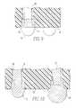
- FIG. 6an embodiment of the attachment of substrate contact 12 to end of the elongated conductor 8 is shown.
- the substrate contact 12is fused to the end of elongated conductor 8 with a butt joint.
- a portion of the tail end of each elongated conductor 8has a passivated surface 17 .
- Passivated surface 17ensures that solder, used during the attachment process, does not wick along the sides of elongated conductor 8 and potentially enter clearance 18 during substrate contact reflow.
- clearance 18accommodates differences in Coefficients of Thermal Expansion. Accordingly, if solder enters clearance 18 , the reliability of a corresponding solder joint is jeopardized as interface member 10 expands and contracts. Therefore, an anti-solder wicking or non-solder wettable material is applied to the surface 17 .
- One preferred material for this purposeis nickel plating. While not intending to be bound by any particular theory, it is believed that the solder resistant feature of this nickel plated area results from or is enhanced by the oxidation of the nickel plating, for example, by laser oxidation, steam exposure or ambient air exposure. Other solder wick resistant materials are believed to be useable for this purpose, such as fluorine containing solder resist coatings. Alternatively, a combination of nickel and fluorine could be used.
- FIG. 7depicts a second embodiment of the substrate contact and elongated conductor 8 interface.
- the end of elongated conductor 8is beveled.
- solder filet 21is formed between substrate contact 12 and the end of elongated conductor 8 during the attachment of substrate contact 12 to elongated conductor 8 .
- This second embodimentalso reduces the potential for solder to wick into the clearance 18 by capturing solder within a bevel.
- each well 11is substantially uniform in size and shape and provides several features of importance with respect to the present invention. Referring to FIG. 9, for example, each well 11 ensures that a highly uniform amount of solder paste 19 is received therein using a process such as a simple deposit and squeegee operation. Thus, the amount of solder available for securing each substrate contact onto an end of elongated conductor 8 is substantially uniform.
- the wells 11locate the position of each substrate contact in the lateral X-Y directions prior to attachment of the substrate contacts in the Z direction with respect to the bottom surface of interface member 10 and the end of elongated conductor 8 . After solder reflow and best shown in FIG. 6, the solder contained in paste 19 in well 11 increases substrate contact 12 size by area 16 .
- the size of area 16is affected by the height of the tip of conductor 8 within well 11 .
- the amount of solder paste deposited in each well 11is altered by the variation in elongated conductor 8 height. For example, a conductor 8 tip that is higher in well 11 will displace more solder paste; whereas, a conductor 8 tip that is lower in well 11 will displace less solder paste. If less paste is available in the well, during reflow of the solder paste less paste is available to coalesce around the substrate contact, resulting in a slightly smaller substrate contact 12 . A smaller substrate contact will result in a lower height. On the other hand, when more paste is available in the well a larger substrate contact will result, corresponding to a higher substrate contact height.
- the process abovedescribes a substrate contact attachment via the use of preformed substrate contacts 12 .
- the substrate contact interfacecan be formed without the use of preformed substrate contacts.
- FIG. 10there is shown a method of substrate contact 12 attachment using only solder paste.
- a prespecified amount of solder pasteis deposited in and over well 11 .
- This prespecified amount of solder pastecan be deposited by a commercial dispensing machine such as a CAM/A LOT 1818 available from Camelot Systems, Inc.
- the connectoris heated above the solder paste melting point. The solder within the paste then coalesces into a substrate contact 12 , which forms on the end of elongated conductor 8 .
- variable volume of pastewill effect the size and coplanarity of the substrate contacts. Similar to the preformed substrate contact method, the displacement of solder paste by the height of conductor 8 within well 11 will affect the final coplanarity in this method as well.
- coplanarity of the substrate mounting face of a connector utilizing substrate contact mountingis critical with any SMT device.
- connector 1there are two primary factors that influence the coplanarity of the connector to circuit substrate interface: (1) the coplanarity of the end surfaces, i.e., the tips, of elongated conductors 8 ; and (2) the coplanarity of substrate contacts 12 .
- the coplanarity of the tips of elongated conductors 8is affected by a variety of factors such as length of the conductor 8 , uniformity of the bends, the ability to keep the conductors consistently parallel and the like. As a result, it is extremely difficult to maintain the conductor tips within the final coplanarity requirement of the circuit substrate manufacturers while maintaining high yields and low costs.
- the restrictive coplanarity requirements for the completed connector 1is met while imposing a less restrictive coplanarity requirement on the tips of elongated conductors 8 .
- FIG. 11there is shown an exemplary graph of the coplanarity of the tips of elongated conductors 8 before the attachment of substrate contacts 12 (curve 32 ) versus the coplanarity of elongated conductors 8 with the attached substrate contacts 12 (curve 34 ).
- the units along the abscissarepresents different samples used in the coplanarity measurement.
- the units along the ordinaterepresent unit sample height labeled 0 , 1 , 2 and so on; however, these units are labeled to merely illustrate the relative relationship between the tip position and corresponding substrate contact height. Actual units and values will vary depending on factors such as well dimensions and substrate contact size.
- Curve 32represents the height of an elongated conductor tip as measured above the bottom of well 11 (see also FIG. 6 ).
- the measured tip heightis 0 units.
- the tip heightis about 0.75 and so on.
- the tip heightis about 4 units.
- Curve 34represents the height above the bottom of well 11 of the same tip after attachment of the substrate contact 12 (see also FIG. 6 ).
- the corresponding height after attachment of substrate contact 12is about 4.5 units.
- the corresponding substrate contact heightis about 5 units and so on.
- the substrate contact heightis about than 6.5 units.
- Comparing the curves 32 and 34illustrates that the process of attaching substrate contact 12 to the end of conductor 8 absorbs some of the variations in coplanarity of the tips of conductors 8 .
- the difference between the tip height (preattachment curve 32 ) and the substrate contact height (post attachment curve 34 )is about 4.5 units.
- the tip heightis about 4 units
- the substrate contact heightis about 6.5 units, for a difference of only 2.5 unit.
- the total change in tip height over the enter range of sampleswas about 4 units, but the total change of substrate contact height over the same sample range was only about 2 units.
- a typical connector before substrate contact attachmentwill have a number of elongated conductors 8 with different tip heights. If, for example, one conductor 8 has a tip height of 0 (i.e., the tip is exactly flush with the bottom of the well) and another connector has a tip height of 4 units, the coplanarity between the tips would be about 4 units. Under some circumstances this coplanarity variation of 4 units may be unacceptable. However, after the attachment of substrate contacts 12 according to the methods described herein, the corresponding substrate contact heights will be 4.5 units and 6.5 units respectively, for a final coplanarity of about 2 units. Significantly, the final coplanarity is only 2 units versus 4 units.
- a connector 1can be constructed with a higher tolerance for elongated conductors coplanarity than would be possible otherwise.
- the quality of substrate contact 12 attachmentis enhanced by the application of an anti-migration or anti-wicking solution to an area in and around well 11 .
- an anti-migration or anti-wicking solutionWithout the anti-migration solution, substrate contacts may form unevenly, sometimes wicking to the well edges. With the anti-migrations solution applied, solder is repelled from the well edges and forms more uniform substrate contacts on the ends of elongated conductors 8 .
- the preferred anti-migration solutionis oleophobic-hydrophobic fluoropolymer. Such a solution is commercial available from 3M corporation under the Fluorad brand name.
- the substrate contactwill preferably be a solder ball.
- the fusible elementcan also have a shape other than a sphere.
- the ends of elongated conductors 8will extend into well 11 by a sufficient amount to present adequate surface area for the substrate contact to fuse to, and will usually preferably extend into the recess from about 25 percent to 75 percent and more preferably to about 50 percent of the depth of the recess as previously mentioned.
- the recessesordinarily will be circular, square or the shape of any other regular polygon in cross-section.
- the conductive elementWhen the conductive element is solder, it will preferably be an alloy which is in the range of about 3% Sn and 97% Pb to about 100% Sn and 0% Pb. More preferably the alloy will be eutectic which is 63% Sn and 37% Pb and has a melting point of 183° C. Typically, a “hard” solder alloy with a higher lead content would be used for mating to materials such as ceramics. The “hard” substrate contact will “mushroom” or deform slightly as it softens under typical SMT conditions, but will not melt . A “soft” eutectic ball is used for attachment to printed circuit boards and will usually reflow and reform itself under typical SMT conditions.
- solders known to be suitable for electronic purposesare also believed to be acceptable for use in this method.
- Such soldersinclude, without limitation, electronically acceptable tin-antimony, tin-silver and lead silver alloys and indium. Before the substrate contact or other conductive element is positioned in a recess, that recess would usually be filled with solder paste.
- a body of material which is not fusible at SMT temperaturesmay be attached by reflow of the solder paste in the recesses onto the contacts.
- the connector mounting interfacewould comprise a plurality of infusible spheres in a tightly coplanar array. Such a connector would be secured on a substrate by conventional SMT techniques.
- solder pastes or creamsincorporating any conventional organic or inorganic solder flux may be adapted for use in this method
- a no clean solder paste or creamis preferred.
- solder pastes or creamswould include a solder alloy in the form of a fine powder suspended in a suitable fluxing material. This powder will ordinarily be an alloy and not a mixture of constituents. The ratio of solder to flux will ordinarily be high and in the range of 80%-95% by weight solder or approximately 50% by volume. A solder cream will be formed when the solder material is suspended in a rosin flux.
- the rosin fluxwill be a white rosin or a low activity rosin flux, although for various purposes activated or superactivated rosins may be used.
- a solder pastewill be formed when a solder alloy in the form of a fine powder is suspended in an organic acid flux or an inorganic acid flux.
- organic acidsmay be selected from lactic, oleic, stearic, phthalic, citric or other similar acids.
- Such inorganic acidsmay be selected from hydrochloric, hydrofluoric and orthophosphoric acid.
- Cream or pastemay be applied by brushing, screening, or extruding onto the surface which may advantageously have been gradually preheated to ensure good wetting.
- Heatingis preferably conducted in a panel infra red (IR) solder reflow conveyor oven.
- the connectorwould then be heated to a temperature above the melting point of the solder within the solder paste.
Landscapes
- Engineering & Computer Science (AREA)
- Manufacturing & Machinery (AREA)
- Microelectronics & Electronic Packaging (AREA)
- Coupling Device And Connection With Printed Circuit (AREA)
- Manufacturing Of Electrical Connectors (AREA)
- Multi-Conductor Connections (AREA)
Abstract
Description
Claims (15)
Priority Applications (2)
| Application Number | Priority Date | Filing Date | Title |
|---|---|---|---|
| US09/564,760US6247635B1 (en) | 1996-11-14 | 2000-05-04 | High density connector having a ball type of contact surface |
| US09/845,631US6454157B2 (en) | 1996-11-14 | 2001-04-30 | High density connector having a ball type of contact surface |
Applications Claiming Priority (3)
| Application Number | Priority Date | Filing Date | Title |
|---|---|---|---|
| US3079996P | 1996-11-14 | 1996-11-14 | |
| US08/851,165US6139336A (en) | 1996-11-14 | 1997-05-02 | High density connector having a ball type of contact surface |
| US09/564,760US6247635B1 (en) | 1996-11-14 | 2000-05-04 | High density connector having a ball type of contact surface |
Related Parent Applications (1)
| Application Number | Title | Priority Date | Filing Date |
|---|---|---|---|
| US08/851,165DivisionUS6139336A (en) | 1996-11-14 | 1997-05-02 | High density connector having a ball type of contact surface |
Related Child Applications (1)
| Application Number | Title | Priority Date | Filing Date |
|---|---|---|---|
| US09/845,631ContinuationUS6454157B2 (en) | 1996-11-14 | 2001-04-30 | High density connector having a ball type of contact surface |
Publications (1)
| Publication Number | Publication Date |
|---|---|
| US6247635B1true US6247635B1 (en) | 2001-06-19 |
Family
ID=26706486
Family Applications (3)
| Application Number | Title | Priority Date | Filing Date |
|---|---|---|---|
| US08/851,165Expired - LifetimeUS6139336A (en) | 1996-11-14 | 1997-05-02 | High density connector having a ball type of contact surface |
| US09/564,760Expired - LifetimeUS6247635B1 (en) | 1996-11-14 | 2000-05-04 | High density connector having a ball type of contact surface |
| US09/845,631Expired - LifetimeUS6454157B2 (en) | 1996-11-14 | 2001-04-30 | High density connector having a ball type of contact surface |
Family Applications Before (1)
| Application Number | Title | Priority Date | Filing Date |
|---|---|---|---|
| US08/851,165Expired - LifetimeUS6139336A (en) | 1996-11-14 | 1997-05-02 | High density connector having a ball type of contact surface |
Family Applications After (1)
| Application Number | Title | Priority Date | Filing Date |
|---|---|---|---|
| US09/845,631Expired - LifetimeUS6454157B2 (en) | 1996-11-14 | 2001-04-30 | High density connector having a ball type of contact surface |
Country Status (8)
| Country | Link |
|---|---|
| US (3) | US6139336A (en) |
| EP (1) | EP0843383B1 (en) |
| JP (1) | JP4018213B2 (en) |
| KR (1) | KR100517098B1 (en) |
| CN (1) | CN1160833C (en) |
| DE (4) | DE69733243T2 (en) |
| SG (1) | SG67440A1 (en) |
| TW (1) | TW374959B (en) |
Cited By (14)
| Publication number | Priority date | Publication date | Assignee | Title |
|---|---|---|---|---|
| US20020008326A1 (en)* | 2000-05-12 | 2002-01-24 | Nec Corporation | Electrode structure of a carrier substrate of a semiconductor device |
| US6641410B2 (en) | 2001-06-07 | 2003-11-04 | Teradyne, Inc. | Electrical solder ball contact |
| US6679709B2 (en) | 2001-07-13 | 2004-01-20 | Moldec Co., Ltd. | Connector and method for manufacturing same |
| US6695623B2 (en)* | 2001-05-31 | 2004-02-24 | International Business Machines Corporation | Enhanced electrical/mechanical connection for electronic devices |
| US6969286B1 (en) | 2004-06-28 | 2005-11-29 | Samtec, Inc. | Connector having improved contacts with fusible members |
| US20060196857A1 (en)* | 2005-03-03 | 2006-09-07 | Samtec, Inc. | Methods of manufacturing electrical contacts having solder stops |
| US7476110B2 (en) | 1996-10-10 | 2009-01-13 | Fci Americas Technology, Inc. | High density connector and method of manufacture |
| US20110287666A1 (en)* | 2007-12-20 | 2011-11-24 | Molex Incorporated | Anti-wicking terminal and connector |
| US8834181B2 (en) | 2012-04-18 | 2014-09-16 | Fci Americas Technology Llc | Straddle mount electrical connector with fusible elements |
| US10320098B2 (en) | 2017-04-28 | 2019-06-11 | Fci Usa Llc | High frequency BGA connector |
| US10396481B2 (en) | 2014-10-23 | 2019-08-27 | Fci Usa Llc | Mezzanine electrical connector |
| US10404014B2 (en) | 2017-02-17 | 2019-09-03 | Fci Usa Llc | Stacking electrical connector with reduced crosstalk |
| US10405448B2 (en) | 2017-04-28 | 2019-09-03 | Fci Usa Llc | High frequency BGA connector |
| US11735879B2 (en) | 2021-03-09 | 2023-08-22 | Atl Technology, Llc | Adaptor for converting a ball grid array interface into a pin interface |
Families Citing this family (122)
| Publication number | Priority date | Publication date | Assignee | Title |
|---|---|---|---|---|
| US6939173B1 (en) | 1995-06-12 | 2005-09-06 | Fci Americas Technology, Inc. | Low cross talk and impedance controlled electrical connector with solder masses |
| US6024584A (en) | 1996-10-10 | 2000-02-15 | Berg Technology, Inc. | High density connector |
| US6093035A (en)* | 1996-06-28 | 2000-07-25 | Berg Technology, Inc. | Contact for use in an electrical connector |
| US6241535B1 (en) | 1996-10-10 | 2001-06-05 | Berg Technology, Inc. | Low profile connector |
| EP1441417A3 (en)* | 1996-10-10 | 2004-12-01 | Fci | High density connector and method of manufacture |
| US6042389A (en)* | 1996-10-10 | 2000-03-28 | Berg Technology, Inc. | Low profile connector |
| US6139336A (en) | 1996-11-14 | 2000-10-31 | Berg Technology, Inc. | High density connector having a ball type of contact surface |
| US5975921A (en)* | 1997-10-10 | 1999-11-02 | Berg Technology, Inc. | High density connector system |
| US6431889B1 (en) | 1997-12-23 | 2002-08-13 | Berg Technology, Inc. | High density edge card connector |
| SG85609A1 (en)* | 1997-12-23 | 2002-01-15 | Connector Systems Tech Nv | High density edge card connector |
| EP1053571A4 (en)* | 1998-01-08 | 2001-03-28 | Berg Electronics Mfg | High speed connector |
| US6530790B1 (en) | 1998-11-24 | 2003-03-11 | Teradyne, Inc. | Electrical connector |
| WO2000077887A1 (en)* | 1999-06-16 | 2000-12-21 | Fci 's-Hertogenbosch B.V. | Connector, method for manufacturing such a connector and contact element for a connector |
| NL1012361C2 (en)* | 1999-06-16 | 2000-12-19 | Berg Electronics Mfg | Connector has contact elements mounted in housing, in which grooves extend transversely |
| TW471743U (en) | 2000-08-25 | 2002-01-01 | Jau Pei Cheng | Electrical connector |
| JP3467460B2 (en)* | 2000-09-05 | 2003-11-17 | シャープ株式会社 | Jack type photoelectric sharing connection device |
| US6869292B2 (en) | 2001-07-31 | 2005-03-22 | Fci Americas Technology, Inc. | Modular mezzanine connector |
| CN100483886C (en)* | 2001-11-14 | 2009-04-29 | Fci公司 | Crosstalk reduction for electrical connectors |
| US7390200B2 (en) | 2001-11-14 | 2008-06-24 | Fci Americas Technology, Inc. | High speed differential transmission structures without grounds |
| US20050196987A1 (en)* | 2001-11-14 | 2005-09-08 | Shuey Joseph B. | High density, low noise, high speed mezzanine connector |
| US6981883B2 (en) | 2001-11-14 | 2006-01-03 | Fci Americas Technology, Inc. | Impedance control in electrical connectors |
| US6994569B2 (en) | 2001-11-14 | 2006-02-07 | Fci America Technology, Inc. | Electrical connectors having contacts that may be selectively designated as either signal or ground contacts |
| US20040018773A1 (en)* | 2002-07-29 | 2004-01-29 | Fci Americas Technology, Inc. | Printed circuit board assembly having a BGA connection |
| US7008250B2 (en) | 2002-08-30 | 2006-03-07 | Fci Americas Technology, Inc. | Connector receptacle having a short beam and long wipe dual beam contact |
| US7270573B2 (en)* | 2002-08-30 | 2007-09-18 | Fci Americas Technology, Inc. | Electrical connector with load bearing features |
| US6786391B2 (en)* | 2002-10-16 | 2004-09-07 | Kac Holdings, Inc. | Method of controlling solder deposition utilizing two fluxes and preform |
| US6732904B1 (en)* | 2002-10-21 | 2004-05-11 | Feng-Chien Hsu | Solder ball holding terminal in a BGA arrangement |
| US6623284B1 (en) | 2003-01-07 | 2003-09-23 | Hon Hai Precision Ind. Co., Ltd. | Electrical connector |
| US20040147169A1 (en) | 2003-01-28 | 2004-07-29 | Allison Jeffrey W. | Power connector with safety feature |
| KR100443999B1 (en)* | 2003-02-28 | 2004-08-21 | 주식회사 파이컴 | Interconnector for Printed Circuit Board, method thereby and interconnector assembly having it |
| US7018246B2 (en)* | 2003-03-14 | 2006-03-28 | Fci Americas Technology, Inc. | Maintenance of uniform impedance profiles between adjacent contacts in high speed grid array connectors |
| US20040198082A1 (en)* | 2003-04-07 | 2004-10-07 | Victor Zaderej | Method of making an electrical connector |
| US6923657B2 (en)* | 2003-07-22 | 2005-08-02 | Tyco Electronics Corporation | Electrical contact with compliant termination leads |
| US7601012B2 (en)* | 2003-07-24 | 2009-10-13 | Ted Ju | Socket connector |
| US7083432B2 (en)* | 2003-08-06 | 2006-08-01 | Fci Americas Technology, Inc. | Retention member for connector system |
| US7524209B2 (en) | 2003-09-26 | 2009-04-28 | Fci Americas Technology, Inc. | Impedance mating interface for electrical connectors |
| WO2005031922A2 (en)* | 2003-09-26 | 2005-04-07 | Fci Americas Technology, Inc. | Improved impedance mating interface for electrical connectors |
| WO2005065254A2 (en) | 2003-12-31 | 2005-07-21 | Fci Americas Technology, Inc. | Electrical power contacts and connectors comprising same |
| US7458839B2 (en) | 2006-02-21 | 2008-12-02 | Fci Americas Technology, Inc. | Electrical connectors having power contacts with alignment and/or restraining features |
| US7242325B2 (en)* | 2004-08-02 | 2007-07-10 | Sony Corporation | Error correction compensating ones or zeros string suppression |
| US7160117B2 (en)* | 2004-08-13 | 2007-01-09 | Fci Americas Technology, Inc. | High speed, high signal integrity electrical connectors |
| US7422447B2 (en)* | 2004-08-19 | 2008-09-09 | Fci Americas Technology, Inc. | Electrical connector with stepped housing |
| US7214104B2 (en)* | 2004-09-14 | 2007-05-08 | Fci Americas Technology, Inc. | Ball grid array connector |
| US7281950B2 (en) | 2004-09-29 | 2007-10-16 | Fci Americas Technology, Inc. | High speed connectors that minimize signal skew and crosstalk |
| FR2876244B1 (en)* | 2004-10-04 | 2007-01-26 | Commissariat Energie Atomique | COMPONENT HAVING A HARD-CONDUCTIVE MICROPOINT ASSEMBLY AND METHOD FOR ELECTRICALLY CONNECTING IT WITH A COMPONENT PROVIDED WITH DUCTILE CONDUCTIVE PROTUBERANCES |
| US7476108B2 (en) | 2004-12-22 | 2009-01-13 | Fci Americas Technology, Inc. | Electrical power connectors with cooling features |
| US7226296B2 (en)* | 2004-12-23 | 2007-06-05 | Fci Americas Technology, Inc. | Ball grid array contacts with spring action |
| US7204699B2 (en)* | 2004-12-27 | 2007-04-17 | Fci Americas Technology, Inc. | Electrical connector with provisions to reduce thermally-induced stresses |
| CN2773931Y (en)* | 2005-01-22 | 2006-04-19 | 富士康(昆山)电脑接插件有限公司 | Electric connector |
| US7384289B2 (en) | 2005-01-31 | 2008-06-10 | Fci Americas Technology, Inc. | Surface-mount connector |
| US7303427B2 (en) | 2005-04-05 | 2007-12-04 | Fci Americas Technology, Inc. | Electrical connector with air-circulation features |
| US7396259B2 (en)* | 2005-06-29 | 2008-07-08 | Fci Americas Technology, Inc. | Electrical connector housing alignment feature |
| US20070051774A1 (en)* | 2005-09-06 | 2007-03-08 | Stipp John N | Method of controlling solder deposition on heat spreader used for semiconductor package |
| US7819708B2 (en)* | 2005-11-21 | 2010-10-26 | Fci Americas Technology, Inc. | Receptacle contact for improved mating characteristics |
| US7425145B2 (en) | 2006-05-26 | 2008-09-16 | Fci Americas Technology, Inc. | Connectors and contacts for transmitting electrical power |
| US7726982B2 (en) | 2006-06-15 | 2010-06-01 | Fci Americas Technology, Inc. | Electrical connectors with air-circulation features |
| US7462924B2 (en)* | 2006-06-27 | 2008-12-09 | Fci Americas Technology, Inc. | Electrical connector with elongated ground contacts |
| US7591655B2 (en) | 2006-08-02 | 2009-09-22 | Tyco Electronics Corporation | Electrical connector having improved electrical characteristics |
| US7670196B2 (en) | 2006-08-02 | 2010-03-02 | Tyco Electronics Corporation | Electrical terminal having tactile feedback tip and electrical connector for use therewith |
| US7753742B2 (en) | 2006-08-02 | 2010-07-13 | Tyco Electronics Corporation | Electrical terminal having improved insertion characteristics and electrical connector for use therewith |
| US7549897B2 (en) | 2006-08-02 | 2009-06-23 | Tyco Electronics Corporation | Electrical connector having improved terminal configuration |
| US8142236B2 (en) | 2006-08-02 | 2012-03-27 | Tyco Electronics Corporation | Electrical connector having improved density and routing characteristics and related methods |
| US7500871B2 (en) | 2006-08-21 | 2009-03-10 | Fci Americas Technology, Inc. | Electrical connector system with jogged contact tails |
| US7713088B2 (en) | 2006-10-05 | 2010-05-11 | Fci | Broadside-coupled signal pair configurations for electrical connectors |
| US7303443B1 (en)* | 2006-10-12 | 2007-12-04 | International Business Machines Corporation | Socket and method for compensating for differing coefficients of thermal expansion |
| US7472477B2 (en) | 2006-10-12 | 2009-01-06 | International Business Machines Corporation | Method for manufacturing a socket that compensates for differing coefficients of thermal expansion |
| US7708569B2 (en) | 2006-10-30 | 2010-05-04 | Fci Americas Technology, Inc. | Broadside-coupled signal pair configurations for electrical connectors |
| US7497736B2 (en) | 2006-12-19 | 2009-03-03 | Fci Americas Technology, Inc. | Shieldless, high-speed, low-cross-talk electrical connector |
| CN201029151Y (en)* | 2006-12-26 | 2008-02-27 | 富士康(昆山)电脑接插件有限公司 | electrical connector |
| US7575445B2 (en)* | 2007-02-21 | 2009-08-18 | Fci Americas Technology, Inc. | Contact protector |
| US7744380B2 (en)* | 2007-02-21 | 2010-06-29 | Fci Americas Technology, Inc | Overmolded electrical contact array |
| US20080203547A1 (en)* | 2007-02-26 | 2008-08-28 | Minich Steven E | Insert molded leadframe assembly |
| US7641500B2 (en) | 2007-04-04 | 2010-01-05 | Fci Americas Technology, Inc. | Power cable connector system |
| US7905731B2 (en) | 2007-05-21 | 2011-03-15 | Fci Americas Technology, Inc. | Electrical connector with stress-distribution features |
| US7811100B2 (en) | 2007-07-13 | 2010-10-12 | Fci Americas Technology, Inc. | Electrical connector system having a continuous ground at the mating interface thereof |
| US7762857B2 (en) | 2007-10-01 | 2010-07-27 | Fci Americas Technology, Inc. | Power connectors with contact-retention features |
| US8764464B2 (en) | 2008-02-29 | 2014-07-01 | Fci Americas Technology Llc | Cross talk reduction for high speed electrical connectors |
| US8062051B2 (en) | 2008-07-29 | 2011-11-22 | Fci Americas Technology Llc | Electrical communication system having latching and strain relief features |
| JP5405582B2 (en) | 2008-11-14 | 2014-02-05 | モレックス インコーポレイテド | Resonance change connector |
| MY155071A (en) | 2008-12-12 | 2015-08-28 | Molex Inc | Resonance modifying connector |
| USD606497S1 (en) | 2009-01-16 | 2009-12-22 | Fci Americas Technology, Inc. | Vertical electrical connector |
| USD610548S1 (en) | 2009-01-16 | 2010-02-23 | Fci Americas Technology, Inc. | Right-angle electrical connector |
| USD640637S1 (en) | 2009-01-16 | 2011-06-28 | Fci Americas Technology Llc | Vertical electrical connector |
| USD608293S1 (en) | 2009-01-16 | 2010-01-19 | Fci Americas Technology, Inc. | Vertical electrical connector |
| USD606496S1 (en) | 2009-01-16 | 2009-12-22 | Fci Americas Technology, Inc. | Right-angle electrical connector |
| USD664096S1 (en) | 2009-01-16 | 2012-07-24 | Fci Americas Technology Llc | Vertical electrical connector |
| US8323049B2 (en) | 2009-01-30 | 2012-12-04 | Fci Americas Technology Llc | Electrical connector having power contacts |
| USD619099S1 (en) | 2009-01-30 | 2010-07-06 | Fci Americas Technology, Inc. | Electrical connector |
| US9277649B2 (en) | 2009-02-26 | 2016-03-01 | Fci Americas Technology Llc | Cross talk reduction for high-speed electrical connectors |
| US8366485B2 (en) | 2009-03-19 | 2013-02-05 | Fci Americas Technology Llc | Electrical connector having ribbed ground plate |
| USD618181S1 (en) | 2009-04-03 | 2010-06-22 | Fci Americas Technology, Inc. | Asymmetrical electrical connector |
| USD618180S1 (en) | 2009-04-03 | 2010-06-22 | Fci Americas Technology, Inc. | Asymmetrical electrical connector |
| US8608510B2 (en) | 2009-07-24 | 2013-12-17 | Fci Americas Technology Llc | Dual impedance electrical connector |
| US8267721B2 (en) | 2009-10-28 | 2012-09-18 | Fci Americas Technology Llc | Electrical connector having ground plates and ground coupling bar |
| US20110104913A1 (en)* | 2009-11-02 | 2011-05-05 | Hinkle Jonathan R | Edge card connector having solder balls and related methods |
| US8616919B2 (en) | 2009-11-13 | 2013-12-31 | Fci Americas Technology Llc | Attachment system for electrical connector |
| CN102725919B (en) | 2009-12-30 | 2015-07-08 | Fci公司 | Electrical connector with impedance tuning ribs |
| JP5585156B2 (en)* | 2010-03-26 | 2014-09-10 | ミツミ電機株式会社 | Thin connector |
| TWM396512U (en)* | 2010-07-30 | 2011-01-11 | Tyco Electronics Holdings Bermuda No 7 Ltd | Card-edge connector |
| US9136634B2 (en) | 2010-09-03 | 2015-09-15 | Fci Americas Technology Llc | Low-cross-talk electrical connector |
| TWM401888U (en) | 2010-09-14 | 2011-04-11 | Hon Hai Prec Ind Co Ltd | Electrical connector |
| US20120282803A1 (en)* | 2011-05-05 | 2012-11-08 | Brocade Communications Systems, Inc. | Double Stack Compact Flash Card Connector |
| EP2624034A1 (en) | 2012-01-31 | 2013-08-07 | Fci | Dismountable optical coupling device |
| USD727852S1 (en) | 2012-04-13 | 2015-04-28 | Fci Americas Technology Llc | Ground shield for a right angle electrical connector |
| USD727268S1 (en) | 2012-04-13 | 2015-04-21 | Fci Americas Technology Llc | Vertical electrical connector |
| US8944831B2 (en) | 2012-04-13 | 2015-02-03 | Fci Americas Technology Llc | Electrical connector having ribbed ground plate with engagement members |
| US9257778B2 (en) | 2012-04-13 | 2016-02-09 | Fci Americas Technology | High speed electrical connector |
| USD718253S1 (en) | 2012-04-13 | 2014-11-25 | Fci Americas Technology Llc | Electrical cable connector |
| USD751507S1 (en) | 2012-07-11 | 2016-03-15 | Fci Americas Technology Llc | Electrical connector |
| US9543703B2 (en) | 2012-07-11 | 2017-01-10 | Fci Americas Technology Llc | Electrical connector with reduced stack height |
| USD745852S1 (en) | 2013-01-25 | 2015-12-22 | Fci Americas Technology Llc | Electrical connector |
| USD720698S1 (en) | 2013-03-15 | 2015-01-06 | Fci Americas Technology Llc | Electrical cable connector |
| CN107678504B (en)* | 2016-08-02 | 2019-11-01 | 纬创资通(中山)有限公司 | expansion card assembly |
| US11239639B2 (en) | 2016-09-30 | 2022-02-01 | TE Connectivity Services Gmbh | Assembly and method for sealing a bundle of wires |
| CN206532914U (en) | 2017-01-20 | 2017-09-29 | 番禺得意精密电子工业有限公司 | Electric connector |
| US10103458B2 (en) | 2017-02-07 | 2018-10-16 | Te Connectivity Corporation | System and method for sealing electrical terminals |
| US10483661B2 (en) | 2017-02-07 | 2019-11-19 | Te Connectivity Corporation | System and method for sealing electrical terminals |
| US10109947B2 (en) | 2017-02-07 | 2018-10-23 | Te Connectivity Corporation | System and method for sealing electrical terminals |
| US10297946B1 (en) | 2018-04-19 | 2019-05-21 | Te Connectivity Corporation | Apparatus and methods for sealing electrical connections |
| US10470313B1 (en) | 2018-07-02 | 2019-11-05 | Te Connectivity Corporation | Solder ball module for contact assembly of an electrical connector |
| US11257612B2 (en) | 2018-07-26 | 2022-02-22 | TE Connectivity Services Gmbh | Assembly and method for sealing a bundle of wires |
| CN114744424B (en)* | 2020-12-24 | 2025-06-06 | 山一电机株式会社 | Connector Kits and Connectors |
Citations (91)
| Publication number | Priority date | Publication date | Assignee | Title |
|---|---|---|---|---|
| US3320658A (en) | 1964-06-26 | 1967-05-23 | Ibm | Method of making electrical connectors and connections |
| US3599326A (en)* | 1969-01-27 | 1971-08-17 | Philco Ford Corp | Method of forming electrical connections with solder resistant surfaces |
| US3719981A (en) | 1971-11-24 | 1973-03-13 | Rca Corp | Method of joining solder balls to solder bumps |
| US3838382A (en) | 1973-07-13 | 1974-09-24 | Itt | Retention system for electrical contacts |
| US3864004A (en) | 1972-11-30 | 1975-02-04 | Du Pont | Circuit board socket |
| US3889364A (en) | 1972-06-02 | 1975-06-17 | Siemens Ag | Method of making soldered electrical connections |
| US4056302A (en) | 1976-06-04 | 1977-11-01 | International Business Machines Corporation | Electrical connection structure and method |
| US4097266A (en) | 1975-01-24 | 1978-06-27 | Senju Metal Industry Co., Ltd. | Microsphere of solder having a metallic core and production thereof |
| EP0043778A1 (en) | 1980-07-09 | 1982-01-13 | Raymond Marc Xavier Gleizes | Method and apparatus for presoldering solder balls on contact strips |
| US4380518A (en) | 1982-01-04 | 1983-04-19 | Western Electric Company, Inc. | Method of producing solder spheres |
| US4396140A (en) | 1981-01-27 | 1983-08-02 | Bell Telephone Laboratories, Incorporated | Method of bonding electronic components |
| US4421266A (en)* | 1981-07-29 | 1983-12-20 | Western Electric Company, Inc. | Handling bodies containing bonding material |
| US4462534A (en) | 1981-12-29 | 1984-07-31 | International Business Machines Corporation | Method of bonding connecting pins to the eyelets of conductors formed on a ceramic substrate |
| JPS6072663A (en) | 1983-09-28 | 1985-04-24 | Fujitsu Ltd | Connecting method of low melting metallic ball |
| US4641426A (en) | 1985-06-21 | 1987-02-10 | Associated Enterprises, Inc. | Surface mount compatible connector system with mechanical integrity |
| US4664309A (en) | 1983-06-30 | 1987-05-12 | Raychem Corporation | Chip mounting device |
| US4678250A (en) | 1985-01-08 | 1987-07-07 | Methode Electronics, Inc. | Multi-pin electrical header |
| US4705205A (en) | 1983-06-30 | 1987-11-10 | Raychem Corporation | Chip carrier mounting device |
| US4722470A (en) | 1986-12-01 | 1988-02-02 | International Business Machines Corporation | Method and transfer plate for applying solder to component leads |
| US4767344A (en) | 1986-08-22 | 1988-08-30 | Burndy Corporation | Solder mounting of electrical contacts |
| US4802862A (en) | 1981-03-30 | 1989-02-07 | North American Specialties Corporation | Solderable electrical contact |
| US4830264A (en) | 1986-10-08 | 1989-05-16 | International Business Machines Corporation | Method of forming solder terminals for a pinless ceramic module |
| US4841101A (en)* | 1987-12-21 | 1989-06-20 | Pollock John A | Hermetically sealed feedthroughs and methods of making same |
| US4871110A (en) | 1987-09-14 | 1989-10-03 | Hitachi, Ltd. | Method and apparatus for aligning solder balls |
| US4884335A (en) | 1985-06-21 | 1989-12-05 | Minnesota Mining And Manufacturing Company | Surface mount compatible connector system with solder strip and mounting connector to PCB |
| JPH0278893A (en) | 1988-09-14 | 1990-03-19 | Sanden Corp | Heat exchanger and manufacture thereof |
| US4986462A (en) | 1988-03-02 | 1991-01-22 | General Dynamics Corporation | Method for cleaning and/or fluxing circuit card assemblies |
| US5024372A (en) | 1989-01-03 | 1991-06-18 | Motorola, Inc. | Method of making high density solder bumps and a substrate socket for high density solder bumps |
| US5060844A (en) | 1990-07-18 | 1991-10-29 | International Business Machines Corporation | Interconnection structure and test method |
| US5093986A (en) | 1990-02-05 | 1992-03-10 | Murata Manufacturing Co., Ltd. | Method of forming bump electrodes |
| US5111991A (en) | 1990-10-22 | 1992-05-12 | Motorola, Inc. | Method of soldering components to printed circuit boards |
| US5118027A (en) | 1991-04-24 | 1992-06-02 | International Business Machines Corporation | Method of aligning and mounting solder balls to a substrate |
| US5129573A (en)* | 1991-10-25 | 1992-07-14 | Compaq Computer Corporation | Method for attaching through-hole devices to a circuit board using solder paste |
| US5145104A (en) | 1991-03-21 | 1992-09-08 | International Business Machines Corporation | Substrate soldering in a reducing atmosphere |
| US5203075A (en) | 1991-08-12 | 1993-04-20 | Inernational Business Machines | Method of bonding flexible circuit to cicuitized substrate to provide electrical connection therebetween using different solders |
| US5207372A (en) | 1991-09-23 | 1993-05-04 | International Business Machines | Method for soldering a semiconductor device to a circuitized substrate |
| US5222649A (en) | 1991-09-23 | 1993-06-29 | International Business Machines | Apparatus for soldering a semiconductor device to a circuitized substrate |
| US5229016A (en) | 1991-08-08 | 1993-07-20 | Microfab Technologies, Inc. | Method and apparatus for dispensing spherical-shaped quantities of liquid solder |
| US5244143A (en) | 1992-04-16 | 1993-09-14 | International Business Machines Corporation | Apparatus and method for injection molding solder and applications thereof |
| US5255839A (en) | 1992-01-02 | 1993-10-26 | Motorola, Inc. | Method for solder application and reflow |
| US5261155A (en) | 1991-08-12 | 1993-11-16 | International Business Machines Corporation | Method for bonding flexible circuit to circuitized substrate to provide electrical connection therebetween using different solders |
| US5269453A (en) | 1992-04-02 | 1993-12-14 | Motorola, Inc. | Low temperature method for forming solder bump interconnections to a plated circuit trace |
| US5275330A (en) | 1993-04-12 | 1994-01-04 | International Business Machines Corp. | Solder ball connect pad-on-via assembly process |
| US5284287A (en) | 1992-08-31 | 1994-02-08 | Motorola, Inc. | Method for attaching conductive balls to a substrate |
| EP0591772A1 (en) | 1992-10-07 | 1994-04-13 | Fujitsu Limited | High-density/long-via laminated connector |
| US5324569A (en) | 1993-02-26 | 1994-06-28 | Hewlett-Packard Company | Composite transversely plastic interconnect for microchip carrier |
| JPH06203896A (en) | 1992-12-29 | 1994-07-22 | Funai Electric Co Ltd | Pin structure for connector |
| US5334046A (en) | 1993-02-22 | 1994-08-02 | Augat Inc. | Circuit card interface system |
| US5346118A (en) | 1993-09-28 | 1994-09-13 | At&T Bell Laboratories | Surface mount solder assembly of leadless integrated circuit packages to substrates |
| US5355283A (en) | 1993-04-14 | 1994-10-11 | Amkor Electronics, Inc. | Ball grid array with via interconnection |
| US5358417A (en) | 1993-08-27 | 1994-10-25 | The Whitaker Corporation | Surface mountable electrical connector |
| US5377902A (en) | 1994-01-14 | 1995-01-03 | Microfab Technologies, Inc. | Method of making solder interconnection arrays |
| US5387139A (en) | 1993-04-30 | 1995-02-07 | The Whitaker Corporation | Method of making a pin grid array and terminal for use therein |
| US5395250A (en) | 1994-01-21 | 1995-03-07 | The Whitaker Corporation | Low profile board to board connector |
| US5410807A (en)* | 1992-02-04 | 1995-05-02 | International Business Machines Corporation | High density electronic connector and method of assembly |
| US5431332A (en) | 1994-02-07 | 1995-07-11 | Motorola, Inc. | Method and apparatus for solder sphere placement using an air knife |
| US5435482A (en) | 1994-02-04 | 1995-07-25 | Lsi Logic Corporation | Integrated circuit having a coplanar solder ball contact array |
| US5442852A (en) | 1993-10-26 | 1995-08-22 | Pacific Microelectronics Corporation | Method of fabricating solder ball array |
| US5445313A (en) | 1992-08-04 | 1995-08-29 | International Business Machines Corporation | Solder particle deposition |
| US5453017A (en) | 1993-11-15 | 1995-09-26 | Berg Technology, Inc. | Solderable connector for high density electronic assemblies |
| US5467913A (en) | 1993-05-31 | 1995-11-21 | Citizen Watch Co., Ltd. | Solder ball supply device |
| US5477933A (en) | 1994-10-24 | 1995-12-26 | At&T Corp. | Electronic device interconnection techniques |
| US5489750A (en) | 1993-03-11 | 1996-02-06 | Matsushita Electric Industrial Co., Ltd. | Method of mounting an electronic part with bumps on a circuit board |
| US5491303A (en) | 1994-03-21 | 1996-02-13 | Motorola, Inc. | Surface mount interposer |
| US5492266A (en) | 1994-08-31 | 1996-02-20 | International Business Machines Corporation | Fine pitch solder deposits on printed circuit board process and product |
| US5495668A (en) | 1994-01-13 | 1996-03-05 | The Furukawa Electric Co., Ltd. | Manufacturing method for a supermicro-connector |
| US5498167A (en) | 1994-04-13 | 1996-03-12 | Molex Incorporated | Board to board electrical connectors |
| US5499487A (en) | 1994-09-14 | 1996-03-19 | Vanguard Automation, Inc. | Method and apparatus for filling a ball grid array |
| US5516030A (en) | 1994-07-20 | 1996-05-14 | Compaq Computer Corporation | Method and apparatus for assembling ball grid array components on printed circuit boards by reflowing before placement |
| US5516032A (en) | 1993-11-17 | 1996-05-14 | Matsushita Electric Industrial Co., Ltd. | Method for forming bump electrode |
| US5519580A (en) | 1994-09-09 | 1996-05-21 | Intel Corporation | Method of controlling solder ball size of BGA IC components |
| US5518410A (en) | 1993-05-24 | 1996-05-21 | Enplas Corporation | Contact pin device for IC sockets |
| US5534127A (en) | 1994-01-11 | 1996-07-09 | Matsushita Electric Industrial Co., Ltd. | Method of forming solder bumps on electrodes of electronic component |
| US5539153A (en) | 1994-08-08 | 1996-07-23 | Hewlett-Packard Company | Method of bumping substrates by contained paste deposition |
| US5542174A (en) | 1994-09-15 | 1996-08-06 | Intel Corporation | Method and apparatus for forming solder balls and solder columns |
| US5577657A (en)* | 1995-09-01 | 1996-11-26 | Ford Motor Company | Method of improved oven reflow soldering |
| WO1996042123A1 (en) | 1995-06-12 | 1996-12-27 | Berg Technology, Inc. | Low cross talk and impedance controlled electrical connector and electrical cable assembly |
| US5591941A (en) | 1993-10-28 | 1997-01-07 | International Business Machines Corporation | Solder ball interconnected assembly |
| US5591049A (en) | 1994-04-21 | 1997-01-07 | Murata Manufacturing Co., Ltd. | High voltage connector |
| US5593322A (en) | 1995-01-17 | 1997-01-14 | Dell Usa, L.P. | Leadless high density connector |
| US5613882A (en) | 1993-03-19 | 1997-03-25 | The Whitaker Corporation | Connector latch and polarizing structure |
| WO1997020454A1 (en) | 1995-11-30 | 1997-06-05 | The Whitaker Corporation | Surface mount socket for an electronic package and contact for use therewith |
| US5643009A (en) | 1996-02-26 | 1997-07-01 | The Whitaker Corporation | Electrical connector having a pivot lock |
| US5692912A (en) | 1995-06-14 | 1997-12-02 | Molex Incorporated | Electrical connector with terminal tail aligning device |
| US5702255A (en) | 1995-11-03 | 1997-12-30 | Advanced Interconnections Corporation | Ball grid array socket assembly |
| US5718607A (en) | 1996-03-01 | 1998-02-17 | Molex Incorporated | System for terminating the shield of a high speed cable |
| US5730606A (en) | 1996-04-02 | 1998-03-24 | Aries Electronics, Inc. | Universal production ball grid array socket |
| EP0836243A2 (en) | 1996-10-10 | 1998-04-15 | Berg Electronics Manufacturing B.V. | High density connector and method of manufacture |
| WO1998015990A1 (en) | 1996-10-10 | 1998-04-16 | Berg Technology, Inc. | Low profile connector |
| US5772451A (en) | 1993-11-16 | 1998-06-30 | Form Factor, Inc. | Sockets for electronic components and methods of connecting to electronic components |
| US6139336A (en) | 1996-11-14 | 2000-10-31 | Berg Technology, Inc. | High density connector having a ball type of contact surface |
Family Cites Families (2)
| Publication number | Priority date | Publication date | Assignee | Title |
|---|---|---|---|---|
| US5536153A (en)* | 1994-06-28 | 1996-07-16 | Edwards; Thomas C. | Non-contact vane-type fluid displacement machine with lubricant separator and sump arrangement |
| US6193143B1 (en)* | 1998-08-05 | 2001-02-27 | Matsushita Electric Industrial Co., Ltd. | Solder bump forming method and mounting apparatus and mounting method of solder ball |
- 1997
- 1997-05-02USUS08/851,165patent/US6139336A/ennot_activeExpired - Lifetime
- 1997-11-12DEDE69733243Tpatent/DE69733243T2/ennot_activeExpired - Lifetime
- 1997-11-12DEDE69737982Tpatent/DE69737982T2/ennot_activeExpired - Lifetime
- 1997-11-12EPEP97119827Apatent/EP0843383B1/ennot_activeExpired - Lifetime
- 1997-11-12DEDE69738847Tpatent/DE69738847D1/ennot_activeExpired - Lifetime
- 1997-11-12DEDE69738037Tpatent/DE69738037T2/ennot_activeExpired - Lifetime
- 1997-11-13SGSG1997004034Apatent/SG67440A1/enunknown
- 1997-11-14TWTW086116993Apatent/TW374959B/ennot_activeIP Right Cessation
- 1997-11-14JPJP31382697Apatent/JP4018213B2/ennot_activeExpired - Lifetime
- 1997-11-14CNCNB971226814Apatent/CN1160833C/ennot_activeExpired - Lifetime
- 2000
- 2000-05-04USUS09/564,760patent/US6247635B1/ennot_activeExpired - Lifetime
- 2001
- 2001-04-30USUS09/845,631patent/US6454157B2/ennot_activeExpired - Lifetime
- 2004
- 2004-10-29KRKR1020040086980Apatent/KR100517098B1/ennot_activeExpired - Lifetime
Patent Citations (95)
| Publication number | Priority date | Publication date | Assignee | Title |
|---|---|---|---|---|
| US3320658A (en) | 1964-06-26 | 1967-05-23 | Ibm | Method of making electrical connectors and connections |
| US3599326A (en)* | 1969-01-27 | 1971-08-17 | Philco Ford Corp | Method of forming electrical connections with solder resistant surfaces |
| US3719981A (en) | 1971-11-24 | 1973-03-13 | Rca Corp | Method of joining solder balls to solder bumps |
| US3889364A (en) | 1972-06-02 | 1975-06-17 | Siemens Ag | Method of making soldered electrical connections |
| US3864004A (en) | 1972-11-30 | 1975-02-04 | Du Pont | Circuit board socket |
| US3838382A (en) | 1973-07-13 | 1974-09-24 | Itt | Retention system for electrical contacts |
| US4097266A (en) | 1975-01-24 | 1978-06-27 | Senju Metal Industry Co., Ltd. | Microsphere of solder having a metallic core and production thereof |
| US4056302A (en) | 1976-06-04 | 1977-11-01 | International Business Machines Corporation | Electrical connection structure and method |
| EP0043778A1 (en) | 1980-07-09 | 1982-01-13 | Raymond Marc Xavier Gleizes | Method and apparatus for presoldering solder balls on contact strips |
| US4396140A (en) | 1981-01-27 | 1983-08-02 | Bell Telephone Laboratories, Incorporated | Method of bonding electronic components |
| US4802862A (en) | 1981-03-30 | 1989-02-07 | North American Specialties Corporation | Solderable electrical contact |
| US4421266A (en)* | 1981-07-29 | 1983-12-20 | Western Electric Company, Inc. | Handling bodies containing bonding material |
| US4462534A (en) | 1981-12-29 | 1984-07-31 | International Business Machines Corporation | Method of bonding connecting pins to the eyelets of conductors formed on a ceramic substrate |
| US4380518A (en) | 1982-01-04 | 1983-04-19 | Western Electric Company, Inc. | Method of producing solder spheres |
| US4664309A (en) | 1983-06-30 | 1987-05-12 | Raychem Corporation | Chip mounting device |
| US4705205A (en) | 1983-06-30 | 1987-11-10 | Raychem Corporation | Chip carrier mounting device |
| JPS6072663A (en) | 1983-09-28 | 1985-04-24 | Fujitsu Ltd | Connecting method of low melting metallic ball |
| US4678250A (en) | 1985-01-08 | 1987-07-07 | Methode Electronics, Inc. | Multi-pin electrical header |
| US4641426A (en) | 1985-06-21 | 1987-02-10 | Associated Enterprises, Inc. | Surface mount compatible connector system with mechanical integrity |
| US4884335A (en) | 1985-06-21 | 1989-12-05 | Minnesota Mining And Manufacturing Company | Surface mount compatible connector system with solder strip and mounting connector to PCB |
| US4767344A (en) | 1986-08-22 | 1988-08-30 | Burndy Corporation | Solder mounting of electrical contacts |
| US4830264A (en) | 1986-10-08 | 1989-05-16 | International Business Machines Corporation | Method of forming solder terminals for a pinless ceramic module |
| US4722470A (en) | 1986-12-01 | 1988-02-02 | International Business Machines Corporation | Method and transfer plate for applying solder to component leads |
| US4871110A (en) | 1987-09-14 | 1989-10-03 | Hitachi, Ltd. | Method and apparatus for aligning solder balls |
| US4841101A (en)* | 1987-12-21 | 1989-06-20 | Pollock John A | Hermetically sealed feedthroughs and methods of making same |
| US4986462A (en) | 1988-03-02 | 1991-01-22 | General Dynamics Corporation | Method for cleaning and/or fluxing circuit card assemblies |
| JPH0278893A (en) | 1988-09-14 | 1990-03-19 | Sanden Corp | Heat exchanger and manufacture thereof |
| US5024372A (en) | 1989-01-03 | 1991-06-18 | Motorola, Inc. | Method of making high density solder bumps and a substrate socket for high density solder bumps |
| US5093986A (en) | 1990-02-05 | 1992-03-10 | Murata Manufacturing Co., Ltd. | Method of forming bump electrodes |
| US5060844A (en) | 1990-07-18 | 1991-10-29 | International Business Machines Corporation | Interconnection structure and test method |
| US5111991A (en) | 1990-10-22 | 1992-05-12 | Motorola, Inc. | Method of soldering components to printed circuit boards |
| US5145104A (en) | 1991-03-21 | 1992-09-08 | International Business Machines Corporation | Substrate soldering in a reducing atmosphere |
| US5118027A (en) | 1991-04-24 | 1992-06-02 | International Business Machines Corporation | Method of aligning and mounting solder balls to a substrate |
| US5229016A (en) | 1991-08-08 | 1993-07-20 | Microfab Technologies, Inc. | Method and apparatus for dispensing spherical-shaped quantities of liquid solder |
| US5261155A (en) | 1991-08-12 | 1993-11-16 | International Business Machines Corporation | Method for bonding flexible circuit to circuitized substrate to provide electrical connection therebetween using different solders |
| US5203075A (en) | 1991-08-12 | 1993-04-20 | Inernational Business Machines | Method of bonding flexible circuit to cicuitized substrate to provide electrical connection therebetween using different solders |
| US5207372A (en) | 1991-09-23 | 1993-05-04 | International Business Machines | Method for soldering a semiconductor device to a circuitized substrate |
| US5222649A (en) | 1991-09-23 | 1993-06-29 | International Business Machines | Apparatus for soldering a semiconductor device to a circuitized substrate |
| US5129573A (en)* | 1991-10-25 | 1992-07-14 | Compaq Computer Corporation | Method for attaching through-hole devices to a circuit board using solder paste |
| US5255839A (en) | 1992-01-02 | 1993-10-26 | Motorola, Inc. | Method for solder application and reflow |
| US5410807A (en)* | 1992-02-04 | 1995-05-02 | International Business Machines Corporation | High density electronic connector and method of assembly |
| US5269453A (en) | 1992-04-02 | 1993-12-14 | Motorola, Inc. | Low temperature method for forming solder bump interconnections to a plated circuit trace |
| US5244143A (en) | 1992-04-16 | 1993-09-14 | International Business Machines Corporation | Apparatus and method for injection molding solder and applications thereof |
| US5445313A (en) | 1992-08-04 | 1995-08-29 | International Business Machines Corporation | Solder particle deposition |
| US5284287A (en) | 1992-08-31 | 1994-02-08 | Motorola, Inc. | Method for attaching conductive balls to a substrate |
| EP0591772A1 (en) | 1992-10-07 | 1994-04-13 | Fujitsu Limited | High-density/long-via laminated connector |
| JPH06203896A (en) | 1992-12-29 | 1994-07-22 | Funai Electric Co Ltd | Pin structure for connector |
| US5334046A (en) | 1993-02-22 | 1994-08-02 | Augat Inc. | Circuit card interface system |
| US5324569A (en) | 1993-02-26 | 1994-06-28 | Hewlett-Packard Company | Composite transversely plastic interconnect for microchip carrier |
| US5409157A (en) | 1993-02-26 | 1995-04-25 | Nagesh; Voddarahalli K. | Composite transversely plastic interconnect for microchip carrier |
| US5489750A (en) | 1993-03-11 | 1996-02-06 | Matsushita Electric Industrial Co., Ltd. | Method of mounting an electronic part with bumps on a circuit board |
| US5613882A (en) | 1993-03-19 | 1997-03-25 | The Whitaker Corporation | Connector latch and polarizing structure |
| US5275330A (en) | 1993-04-12 | 1994-01-04 | International Business Machines Corp. | Solder ball connect pad-on-via assembly process |
| US5355283A (en) | 1993-04-14 | 1994-10-11 | Amkor Electronics, Inc. | Ball grid array with via interconnection |
| US5387139A (en) | 1993-04-30 | 1995-02-07 | The Whitaker Corporation | Method of making a pin grid array and terminal for use therein |
| US5518410A (en) | 1993-05-24 | 1996-05-21 | Enplas Corporation | Contact pin device for IC sockets |
| US5467913A (en) | 1993-05-31 | 1995-11-21 | Citizen Watch Co., Ltd. | Solder ball supply device |
| US5358417A (en) | 1993-08-27 | 1994-10-25 | The Whitaker Corporation | Surface mountable electrical connector |
| US5346118A (en) | 1993-09-28 | 1994-09-13 | At&T Bell Laboratories | Surface mount solder assembly of leadless integrated circuit packages to substrates |
| US5504277A (en) | 1993-10-26 | 1996-04-02 | Pacific Microelectronics Corporation | Solder ball array |
| US5442852A (en) | 1993-10-26 | 1995-08-22 | Pacific Microelectronics Corporation | Method of fabricating solder ball array |
| US5591941A (en) | 1993-10-28 | 1997-01-07 | International Business Machines Corporation | Solder ball interconnected assembly |
| US5453017A (en) | 1993-11-15 | 1995-09-26 | Berg Technology, Inc. | Solderable connector for high density electronic assemblies |
| US5772451A (en) | 1993-11-16 | 1998-06-30 | Form Factor, Inc. | Sockets for electronic components and methods of connecting to electronic components |
| US5516032A (en) | 1993-11-17 | 1996-05-14 | Matsushita Electric Industrial Co., Ltd. | Method for forming bump electrode |
| US5534127A (en) | 1994-01-11 | 1996-07-09 | Matsushita Electric Industrial Co., Ltd. | Method of forming solder bumps on electrodes of electronic component |
| US5495668A (en) | 1994-01-13 | 1996-03-05 | The Furukawa Electric Co., Ltd. | Manufacturing method for a supermicro-connector |
| US5377902A (en) | 1994-01-14 | 1995-01-03 | Microfab Technologies, Inc. | Method of making solder interconnection arrays |
| US5395250A (en) | 1994-01-21 | 1995-03-07 | The Whitaker Corporation | Low profile board to board connector |
| US5435482A (en) | 1994-02-04 | 1995-07-25 | Lsi Logic Corporation | Integrated circuit having a coplanar solder ball contact array |
| US5431332A (en) | 1994-02-07 | 1995-07-11 | Motorola, Inc. | Method and apparatus for solder sphere placement using an air knife |
| US5491303A (en) | 1994-03-21 | 1996-02-13 | Motorola, Inc. | Surface mount interposer |
| US5498167A (en) | 1994-04-13 | 1996-03-12 | Molex Incorporated | Board to board electrical connectors |
| US5591049A (en) | 1994-04-21 | 1997-01-07 | Murata Manufacturing Co., Ltd. | High voltage connector |
| US5516030A (en) | 1994-07-20 | 1996-05-14 | Compaq Computer Corporation | Method and apparatus for assembling ball grid array components on printed circuit boards by reflowing before placement |
| US5539153A (en) | 1994-08-08 | 1996-07-23 | Hewlett-Packard Company | Method of bumping substrates by contained paste deposition |
| US5492266A (en) | 1994-08-31 | 1996-02-20 | International Business Machines Corporation | Fine pitch solder deposits on printed circuit board process and product |
| US5519580A (en) | 1994-09-09 | 1996-05-21 | Intel Corporation | Method of controlling solder ball size of BGA IC components |
| US5499487A (en) | 1994-09-14 | 1996-03-19 | Vanguard Automation, Inc. | Method and apparatus for filling a ball grid array |
| US5542174A (en) | 1994-09-15 | 1996-08-06 | Intel Corporation | Method and apparatus for forming solder balls and solder columns |
| US5477933A (en) | 1994-10-24 | 1995-12-26 | At&T Corp. | Electronic device interconnection techniques |
| US5593322A (en) | 1995-01-17 | 1997-01-14 | Dell Usa, L.P. | Leadless high density connector |
| WO1996042123A1 (en) | 1995-06-12 | 1996-12-27 | Berg Technology, Inc. | Low cross talk and impedance controlled electrical connector and electrical cable assembly |
| US5692912A (en) | 1995-06-14 | 1997-12-02 | Molex Incorporated | Electrical connector with terminal tail aligning device |
| US5577657A (en)* | 1995-09-01 | 1996-11-26 | Ford Motor Company | Method of improved oven reflow soldering |
| US5702255A (en) | 1995-11-03 | 1997-12-30 | Advanced Interconnections Corporation | Ball grid array socket assembly |
| WO1997020454A1 (en) | 1995-11-30 | 1997-06-05 | The Whitaker Corporation | Surface mount socket for an electronic package and contact for use therewith |
| US5746608A (en) | 1995-11-30 | 1998-05-05 | Taylor; Attalee S. | Surface mount socket for an electronic package, and contact for use therewith |
| US5643009A (en) | 1996-02-26 | 1997-07-01 | The Whitaker Corporation | Electrical connector having a pivot lock |
| US5718607A (en) | 1996-03-01 | 1998-02-17 | Molex Incorporated | System for terminating the shield of a high speed cable |
| US5730606A (en) | 1996-04-02 | 1998-03-24 | Aries Electronics, Inc. | Universal production ball grid array socket |
| EP0836243A2 (en) | 1996-10-10 | 1998-04-15 | Berg Electronics Manufacturing B.V. | High density connector and method of manufacture |
| WO1998015990A1 (en) | 1996-10-10 | 1998-04-16 | Berg Technology, Inc. | Low profile connector |
| WO1998015989A1 (en) | 1996-10-10 | 1998-04-16 | Berg Technology, Inc. | High density connector and method of manufacture |
| US6139336A (en) | 1996-11-14 | 2000-10-31 | Berg Technology, Inc. | High density connector having a ball type of contact surface |
Cited By (29)
| Publication number | Priority date | Publication date | Assignee | Title |
|---|---|---|---|---|
| US8167630B2 (en) | 1996-10-10 | 2012-05-01 | Fci Americas Technology Llc | High density connector and method of manufacture |
| US7476110B2 (en) | 1996-10-10 | 2009-01-13 | Fci Americas Technology, Inc. | High density connector and method of manufacture |
| US6765293B2 (en)* | 2000-05-12 | 2004-07-20 | Nec Corporation | Electrode structure of a carrier substrate of a semiconductor device |
| US20020008326A1 (en)* | 2000-05-12 | 2002-01-24 | Nec Corporation | Electrode structure of a carrier substrate of a semiconductor device |
| US6695623B2 (en)* | 2001-05-31 | 2004-02-24 | International Business Machines Corporation | Enhanced electrical/mechanical connection for electronic devices |
| US6641410B2 (en) | 2001-06-07 | 2003-11-04 | Teradyne, Inc. | Electrical solder ball contact |
| US6679709B2 (en) | 2001-07-13 | 2004-01-20 | Moldec Co., Ltd. | Connector and method for manufacturing same |
| US20050287879A1 (en)* | 2004-06-28 | 2005-12-29 | Samtec, Inc. | Connector having improved contacts with fusible members |
| US20050287844A1 (en)* | 2004-06-28 | 2005-12-29 | Samtec Inc. | Connector having improved contacts with fusible members |
| US20050287832A1 (en)* | 2004-06-28 | 2005-12-29 | Samtec, Inc. | Connector having improved contacts with fusible members |
| US20050287830A1 (en)* | 2004-06-28 | 2005-12-29 | Samtec, Inc. | Connector having improved contacts with fusible members |
| US20050287845A1 (en)* | 2004-06-28 | 2005-12-29 | Samtec Inc. | Connector having improved contacts with fusible members |
| US20050287831A1 (en)* | 2004-06-28 | 2005-12-29 | Samtec, Inc. | Connector having improved contacts with fusible members |
| US7052337B2 (en) | 2004-06-28 | 2006-05-30 | Samtec, Inc. | Connector having improved contacts with fusible members |
| US6979238B1 (en) | 2004-06-28 | 2005-12-27 | Samtec, Inc. | Connector having improved contacts with fusible members |
| US7125293B2 (en) | 2004-06-28 | 2006-10-24 | Samtec, Inc. | Connector having improved contacts with fusible members |
| US7159312B2 (en) | 2004-06-28 | 2007-01-09 | Samtec, Inc. | Connector having improved contacts with fusible members |
| US7178232B2 (en) | 2004-06-28 | 2007-02-20 | Samtec, Inc. | Connector having improved contacts with fusible members |
| US6969286B1 (en) | 2004-06-28 | 2005-11-29 | Samtec, Inc. | Connector having improved contacts with fusible members |
| US20060196857A1 (en)* | 2005-03-03 | 2006-09-07 | Samtec, Inc. | Methods of manufacturing electrical contacts having solder stops |
| US20110287666A1 (en)* | 2007-12-20 | 2011-11-24 | Molex Incorporated | Anti-wicking terminal and connector |
| US8454397B2 (en)* | 2007-12-20 | 2013-06-04 | Molex Incorporated | Anti-wicking terminal and connector |
| US8834181B2 (en) | 2012-04-18 | 2014-09-16 | Fci Americas Technology Llc | Straddle mount electrical connector with fusible elements |
| US10396481B2 (en) | 2014-10-23 | 2019-08-27 | Fci Usa Llc | Mezzanine electrical connector |
| US10404014B2 (en) | 2017-02-17 | 2019-09-03 | Fci Usa Llc | Stacking electrical connector with reduced crosstalk |
| US10320098B2 (en) | 2017-04-28 | 2019-06-11 | Fci Usa Llc | High frequency BGA connector |
| US10405448B2 (en) | 2017-04-28 | 2019-09-03 | Fci Usa Llc | High frequency BGA connector |
| US11337327B2 (en) | 2017-04-28 | 2022-05-17 | Fci Usa Llc | High frequency BGA connector |
| US11735879B2 (en) | 2021-03-09 | 2023-08-22 | Atl Technology, Llc | Adaptor for converting a ball grid array interface into a pin interface |
Also Published As
| Publication number | Publication date |
|---|---|
| DE69738037D1 (en) | 2007-09-27 |
| DE69733243T2 (en) | 2006-01-19 |
| JP4018213B2 (en) | 2007-12-05 |
| US6139336A (en) | 2000-10-31 |
| TW374959B (en) | 1999-11-21 |
| DE69738847D1 (en) | 2008-08-28 |
| CN1160833C (en) | 2004-08-04 |
| CN1183656A (en) | 1998-06-03 |
| US20010015373A1 (en) | 2001-08-23 |
| SG67440A1 (en) | 1999-09-21 |
| EP0843383A2 (en) | 1998-05-20 |
| DE69737982D1 (en) | 2007-09-13 |
| EP0843383B1 (en) | 2005-05-11 |
| DE69738037T2 (en) | 2008-04-30 |
| KR100517098B1 (en) | 2005-10-19 |
| DE69733243D1 (en) | 2005-06-16 |
| DE69737982T2 (en) | 2008-05-08 |
| JPH10284192A (en) | 1998-10-23 |
| EP0843383A3 (en) | 1998-12-23 |
| US6454157B2 (en) | 2002-09-24 |
Similar Documents
| Publication | Publication Date | Title |
|---|---|---|
| US6247635B1 (en) | High density connector having a ball type of contact surface | |
| US7802999B2 (en) | High density connector and method of manufacture | |
| US6079991A (en) | Method for placing contact on electrical connector | |
| US6093035A (en) | Contact for use in an electrical connector | |
| WO1998015991A9 (en) | High density connector and method of manufacture | |
| EP1536521B1 (en) | High density connector having a ball type of contact surface | |
| EP1311031B1 (en) | High density connector | |
| CA2404792C (en) | High density connector and method of manufacture | |
| CA2455080C (en) | High density connector and method of manufacture | |
| CA2497606C (en) | High density connector and method of manufacture |
Legal Events
| Date | Code | Title | Description |
|---|---|---|---|
| STCF | Information on status: patent grant | Free format text:PATENTED CASE | |
| AS | Assignment | Owner name:FCI AMERICAS TECHNOLOGY, INC., NEVADA Free format text:CHANGE OF NAME;ASSIGNOR:BERG TECHNOLOGY, INC.;REEL/FRAME:012581/0134 Effective date:19990611 | |
| FPAY | Fee payment | Year of fee payment:4 | |
| AS | Assignment | Owner name:BANC OF AMERICA SECURITIES LIMITED, AS SECURITY AG Free format text:SECURITY AGREEMENT;ASSIGNOR:FCI AMERICAS TECHNOLOGY, INC.;REEL/FRAME:017400/0192 Effective date:20060331 | |
| FPAY | Fee payment | Year of fee payment:8 | |
| AS | Assignment | Owner name:FCI AMERICAS TECHNOLOGY, INC., NEVADA Free format text:CHANGE OF NAME;ASSIGNOR:BERG TECHNOLOGY, INC.;REEL/FRAME:026064/0565 Effective date:19990611 Owner name:FCI AMERICAS TECHNOLOGY LLC, NEVADA Free format text:CONVERSION TO LLC;ASSIGNOR:FCI AMERICAS TECHNOLOGY, INC.;REEL/FRAME:026064/0573 Effective date:20090930 | |
| FPAY | Fee payment | Year of fee payment:12 | |
| AS | Assignment | Owner name:FCI AMERICAS TECHNOLOGY LLC (F/K/A FCI AMERICAS TE Free format text:RELEASE OF PATENT SECURITY INTEREST AT REEL/FRAME NO. 17400/0192;ASSIGNOR:BANC OF AMERICA SECURITIES LIMITED;REEL/FRAME:029377/0632 Effective date:20121026 | |
| AS | Assignment | Owner name:WILMINGTON TRUST (LONDON) LIMITED, UNITED KINGDOM Free format text:SECURITY AGREEMENT;ASSIGNOR:FCI AMERICAS TECHNOLOGY LLC;REEL/FRAME:031896/0696 Effective date:20131227 | |
| AS | Assignment | Owner name:FCI AMERICAS TECHNOLOGY LLC, NEVADA Free format text:RELEASE BY SECURED PARTY;ASSIGNOR:WILMINGTON TRUST (LONDON) LIMITED;REEL/FRAME:037484/0169 Effective date:20160108 |