US6245692B1 - Method to selectively heat semiconductor wafers - Google Patents
Method to selectively heat semiconductor wafersDownload PDFInfo
- Publication number
- US6245692B1 US6245692B1US09/448,349US44834999AUS6245692B1US 6245692 B1US6245692 B1US 6245692B1US 44834999 AUS44834999 AUS 44834999AUS 6245692 B1US6245692 B1US 6245692B1
- Authority
- US
- United States
- Prior art keywords
- wafer
- temperature
- film
- heating
- reaction
- Prior art date
- Legal status (The legal status is an assumption and is not a legal conclusion. Google has not performed a legal analysis and makes no representation as to the accuracy of the status listed.)
- Expired - Lifetime
Links
Images

Classifications
- H—ELECTRICITY
- H01—ELECTRIC ELEMENTS
- H01L—SEMICONDUCTOR DEVICES NOT COVERED BY CLASS H10
- H01L21/00—Processes or apparatus adapted for the manufacture or treatment of semiconductor or solid state devices or of parts thereof
- H01L21/02—Manufacture or treatment of semiconductor devices or of parts thereof
- H01L21/04—Manufacture or treatment of semiconductor devices or of parts thereof the devices having potential barriers, e.g. a PN junction, depletion layer or carrier concentration layer
- H01L21/18—Manufacture or treatment of semiconductor devices or of parts thereof the devices having potential barriers, e.g. a PN junction, depletion layer or carrier concentration layer the devices having semiconductor bodies comprising elements of Group IV of the Periodic Table or AIIIBV compounds with or without impurities, e.g. doping materials
- H01L21/30—Treatment of semiconductor bodies using processes or apparatus not provided for in groups H01L21/20 - H01L21/26
- H01L21/324—Thermal treatment for modifying the properties of semiconductor bodies, e.g. annealing, sintering
- H—ELECTRICITY
- H10—SEMICONDUCTOR DEVICES; ELECTRIC SOLID-STATE DEVICES NOT OTHERWISE PROVIDED FOR
- H10D—INORGANIC ELECTRIC SEMICONDUCTOR DEVICES
- H10D30/00—Field-effect transistors [FET]
- H10D30/01—Manufacture or treatment
- H10D30/021—Manufacture or treatment of FETs having insulated gates [IGFET]
- H10D30/0212—Manufacture or treatment of FETs having insulated gates [IGFET] using self-aligned silicidation
Definitions
- This inventionrelates to a method of manufacturing semiconductor integrated circuit interconnect structures.
- the inventionrelates more particularly to a method to alter heat flow on a localized basis when heating wafers to elevated temperatures to achieve different processing temperatures by altering the material properties, such as emissivity, absorptivity, and reflectivity, of a portion of a surface by the application of thin films of specified materials.
- This inventionrelates to a method for fabricating semiconductor integrated circuit devices, specifically with a method for fabricating semiconductor integrated circuit devices enabling the creation of temperature differentials.
- Semiconductor integrated circuit devicestypically comprise silicon and multiple layers of vertically stacked metal interconnect layers with dielectric materials disposed between them.
- the fabrication of such devicestypically involves the repeated deposition or growth, patterning, and etching of thin films of semiconductor, metal, and dielectric materials.
- a substantial part of integrated device manufactureinvolves heating the wafers to elevated temperatures to promote a particular chemical reaction or to anneal the structure to achieve a desired metallurgical effect.
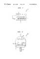
- a batch furnace 10may include a quartz tube 1 inserted into the core 2 of a furnace 3 that is heated resistively, where gas flows through the tube 1 .
- Wafers 4are placed inside the tube 1 and pushed into the core 2 , where a uniform temperature is maintained.
- the heating elements 5heat the core 2 and the wafers 4 with long-wavelength thermal radiation.
- Many wafersmay be processed simultaneously and the cost of operation is divided among the number of wafers in the batch.
- a problem with using a furnaceis that the wafers are susceptible to contamination from the hot processing in the core 2 on which deposited films may accumulate and flake off or through which impurities may diffuse and contaminate wafers 4 .
- a rapid thermal processor 20is shown in FIG. 2.
- a single wafer 11is heated quickly under atmospheric conditions or at low pressure.
- the processing chamber 12is either made of quartz, silicon carbide, stainless steel, or aluminum and has quartz windows 13 through which the optical radiation passes to illuminate the wafer 11 .
- the wafer 11is held, usually on thin quartz pins 18 , in thermal isolation inside chamber 12 .
- An ambient atmosphere inside chamber 12is controlled by gas flow through chamber 12 . Gas flows into the chamber 12 at gas inlet 14 .
- Lamps 15heat the wafer 11 through windows 13 , aided by reflectors 17 above the lamps 15 .
- a measurement systemis placed in a control loop to set wafer temperature.
- an optical pyrometer 16determines the temperature from radiated infrared energy on the back ofthe wafer 11 , but thermocouples can also be used.
- the RTP systemis interfaced with a gas-handling system and a computer that controls system operation.
- a methodis known to apply a thin film on a surface to control reflectivity and emissivity. This film is applied to a wafer in a rapid thermal processor to alter the energy exchange. This method does not address selective application of film on the wafer to alter the temperature.
- Another methodis known for applying a film onto a substrate of a semiconductor, heating the substrate, and removing the layer. This method is used for reducing the effects of semiconductor deformities and does not address temperature differences in heating the wafer.
- the inventionis a method of manufacturing an integrated circuit including the steps of: (1) providing a wafer having a surface; (2) altering material properties, such as emissivity, absorptivity, and reflectivity, of at least one selected portion of the surface to alter heat flow in the portion by depositing at least one layer of film on the portion; (3) heating the wafer to an elevated temperature to initiate a reaction at the portion; and (4) monitoring the temperature of the wafer and terminating the heating when a predetermined period of time has expired.
- material propertiessuch as emissivity, absorptivity, and reflectivity
- FIG. 1is a schematic cross-sectional view of a batch-furnace system used to heat wafers.
- FIG. 2is a schematic cross-sectional view of a rapid thermal processing system used to heat a single wafer.
- FIG. 3is a cross-sectional view of a portion of an integrated circuit.
- FIG. 4is a schematic cross-sectional view of a portion ofthe integrated circuit shown in FIG. 3 manufactured in accordance with the method of the invention.
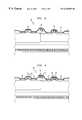
- FIG. 5is a graph of wafer temperature versus time for a wafer with a deposited film (a) and a wafer without a deposited film (b).
- FIG. 6is a schematic cross-sectional view of a portion of the integrated circuit shown in FIG. 3 where the unreacted product is etched.
- FIGS. 3 and 4illustrate aportion of an integrated circuit, which is manufactured in accordance with the method of invention.
- the components of an integrated circuitinclude a wafer 30 having a surface 31 and selected portions 32 of the surface 31 , where a chemical reaction or physical reaction, such as annealing, sintering, or diffusion, may occur in a rapid thermal processor (RTP), or other type of heater.
- RTPrapid thermal processor
- the wafer 30has layers of film 33 deposited on the selected portions 32 .
- the method of the inventionincludes manufacturing an integrated circuit including the steps of; (1) providing a wafer 30 having a surface 31 , as shown in FIG. 3; (2) altering material properties, such as emissivity, absorptivity, and reflectivity, of at least one selected portion 32 of the surface 31 to alter heat flow in the portion 32 by depositing at least one layer of film 33 on the portion 32 , as shown in FIG. 4; (3) heating the wafer 30 to an elevated temperature to initiate a reaction at the portion 32 ; and (4) monitoring the temperature of the wafer 30 to control the heating and terminating the heating when a predetermined period of time has expired.
- the film 33can be made to cause the selected portion of the wafer 30 to be relatively hotter or colder than the surrounding portion ofthe wafer during the RTP process.
- the desired resultwill be selective heating as opposed to selective cooling.
- the heat flowcan be characterized by the equation:
- T sis the source temperature
- T pis the temperature of a portion of the wafer
- the temperature differentialshown in FIG. 5 by a graph of temperature versus time, is derived from the above equations.
- a metal film having an emissivity of 0.1is deposited on a wafer
- a silica film having an emissivity of 0.6is placed selectively on top of the metal film, and the wafer is heated by a heating source at 1600° K, the temperature of the surface with the film at a given time, shown by curve 35 , is greater than the temperature of a surface without the film at the same given time, shown by curve 36 .
- the temperature on curve 35is about 338° K and the corresponding temperature on curve 36 is about 316° K, producing a temperature differential of about 22° K.
- the heat flow at the surface with the silica filmis greater, and while not completely understood, it is believed that the reaction under the film will occur at a different processing temperature than any reaction occurring on the surface without the film. This result was found to agree with an experiment described below using selected films of titanium on silicon. It is also believed that this heating requires less time to produce higher temperatures at various portions on the surface of the wafer. It should be realized that any practical situation may involve a more elaborate theoretical explanation involving the thickness of applied films and their thermal conductivity.
- the filmmay be deposited by low pressure chemical vapor deposition, plasma-enhanced chemical vapor deposition, sputtering, spin-on-glass, molecular beam epitaxy, physical vapor deposition, or combinations thereof
- the filmis deposited on the front of the wafer. Since most of the heat transfer takes place at relatively long wavelengths characteristic of infrared radiation, the exact thickness of the film is not particularly important. However, if the film is too thick, it may have a reverse effect by decreasing the temperature due to the low thermal conductivity of dielectric film.
- film depositeddepends on the cost and ease of the deposition. Particularly preferred are oxide films because they are easily deposited, heated, and patterned and do not have to be removed. Other preferred films are nitrides, metals, silicon, carbon, silicon carbide, or mixtures thereof Carbon and silicon carbide films produce the best emissivity, being close to 1.
- Heatingmay be performed with a rapid thermal processor (RTP), such as a rapid thermal annealer (RTA), or a furnace.
- RTPrapid thermal processor
- RTArapid thermal annealer
- An RTPis preferred because it heats in a short time period, where higher temperature differentials may be achieved. In a furnace, over long periods of time, the temperature differential will decrease and eventually reach 0.
- These methodsmay also include the further step of removing the film from the surface.
- the methodmay include the further steps of stripping the residual photoresist from the wafer; and etching the unreacted product from the wafer.
- the etched wafer 60is shown in FIG. 6 .
- the reaction of Ti and Si forming TiSi 2 , or self-aligning titanium silicidewas examined.
- a wafer having exposed surfaces of Siwas provided.
- the titaniumwas coated with an oxide film of 1000 ⁇ to improve the heat flow.
- the silicidewas selectively formed by a rapid thermal process, in this case, a rapid thermal annealer having a heating lamp and a processing chamber, at a reaction temperature of 650° C.
- a pyrometer of a closed loop temperature control systemsensed an average wafer temperature to control the heating lamp. In this process, the temperature must be comparatively high to achieve complete silicidation on silicon, but as low as possible to avoid any reaction with SiO 2 .
- the amount of TiSi 2 formed with the presence ofthe oxide filmindicated a temperature differential of 20° C. which is consistent with the prior set of calculations. Typically, this method is followed by etching the titanium with a wet etch.
Landscapes
- Engineering & Computer Science (AREA)
- Physics & Mathematics (AREA)
- Condensed Matter Physics & Semiconductors (AREA)
- General Physics & Mathematics (AREA)
- Manufacturing & Machinery (AREA)
- Computer Hardware Design (AREA)
- Microelectronics & Electronic Packaging (AREA)
- Power Engineering (AREA)
- Drying Of Semiconductors (AREA)
- Formation Of Insulating Films (AREA)
- Electrodes Of Semiconductors (AREA)
- Internal Circuitry In Semiconductor Integrated Circuit Devices (AREA)
Abstract
Description

Claims (20)
Priority Applications (5)
| Application Number | Priority Date | Filing Date | Title |
|---|---|---|---|
| US09/448,349US6245692B1 (en) | 1999-11-23 | 1999-11-23 | Method to selectively heat semiconductor wafers |
| EP00310083AEP1104934A3 (en) | 1999-11-23 | 2000-11-13 | Method to selectively heat semiconductor wafers |
| TW089124278ATW464983B (en) | 1999-11-23 | 2000-11-16 | Method to selectively heat semiconductor wafers |
| JP2000355111AJP2001189285A (en) | 1999-11-23 | 2000-11-22 | Method for selectively heating a semiconductor wafer |
| KR1020000069892AKR20010051896A (en) | 1999-11-23 | 2000-11-23 | Method to selectively heat semiconductor wafers |
Applications Claiming Priority (1)
| Application Number | Priority Date | Filing Date | Title |
|---|---|---|---|
| US09/448,349US6245692B1 (en) | 1999-11-23 | 1999-11-23 | Method to selectively heat semiconductor wafers |
Publications (1)
| Publication Number | Publication Date |
|---|---|
| US6245692B1true US6245692B1 (en) | 2001-06-12 |
Family
ID=23779954
Family Applications (1)
| Application Number | Title | Priority Date | Filing Date |
|---|---|---|---|
| US09/448,349Expired - LifetimeUS6245692B1 (en) | 1999-11-23 | 1999-11-23 | Method to selectively heat semiconductor wafers |
Country Status (5)
| Country | Link |
|---|---|
| US (1) | US6245692B1 (en) |
| EP (1) | EP1104934A3 (en) |
| JP (1) | JP2001189285A (en) |
| KR (1) | KR20010051896A (en) |
| TW (1) | TW464983B (en) |
Cited By (48)
| Publication number | Priority date | Publication date | Assignee | Title |
|---|---|---|---|---|
| US6596604B1 (en) | 2002-07-22 | 2003-07-22 | Atmel Corporation | Method of preventing shift of alignment marks during rapid thermal processing |
| US6599831B1 (en)* | 2002-04-30 | 2003-07-29 | Advanced Micro Devices, Inc. | Metal gate electrode using silicidation and method of formation thereof |
| US7138810B2 (en) | 2002-11-08 | 2006-11-21 | Cascade Microtech, Inc. | Probe station with low noise characteristics |
| US7138813B2 (en) | 1999-06-30 | 2006-11-21 | Cascade Microtech, Inc. | Probe station thermal chuck with shielding for capacitive current |
| US7164279B2 (en) | 1995-04-14 | 2007-01-16 | Cascade Microtech, Inc. | System for evaluating probing networks |
| US7176705B2 (en) | 2004-06-07 | 2007-02-13 | Cascade Microtech, Inc. | Thermal optical chuck |
| US7190181B2 (en) | 1997-06-06 | 2007-03-13 | Cascade Microtech, Inc. | Probe station having multiple enclosures |
| US7221172B2 (en) | 2003-05-06 | 2007-05-22 | Cascade Microtech, Inc. | Switched suspended conductor and connection |
| US7221146B2 (en) | 2002-12-13 | 2007-05-22 | Cascade Microtech, Inc. | Guarded tub enclosure |
| US7250779B2 (en) | 2002-11-25 | 2007-07-31 | Cascade Microtech, Inc. | Probe station with low inductance path |
| US7250626B2 (en) | 2003-10-22 | 2007-07-31 | Cascade Microtech, Inc. | Probe testing structure |
| US7268533B2 (en) | 2001-08-31 | 2007-09-11 | Cascade Microtech, Inc. | Optical testing device |
| US7304488B2 (en) | 2002-05-23 | 2007-12-04 | Cascade Microtech, Inc. | Shielded probe for high-frequency testing of a device under test |
| US7330041B2 (en) | 2004-06-14 | 2008-02-12 | Cascade Microtech, Inc. | Localizing a temperature of a device for testing |
| US7330023B2 (en) | 1992-06-11 | 2008-02-12 | Cascade Microtech, Inc. | Wafer probe station having a skirting component |
| US7348787B2 (en) | 1992-06-11 | 2008-03-25 | Cascade Microtech, Inc. | Wafer probe station having environment control enclosure |
| US7352168B2 (en) | 2000-09-05 | 2008-04-01 | Cascade Microtech, Inc. | Chuck for holding a device under test |
| US7355420B2 (en) | 2001-08-21 | 2008-04-08 | Cascade Microtech, Inc. | Membrane probing system |
| US7362115B2 (en) | 2003-12-24 | 2008-04-22 | Cascade Microtech, Inc. | Chuck with integrated wafer support |
| US7368925B2 (en) | 2002-01-25 | 2008-05-06 | Cascade Microtech, Inc. | Probe station with two platens |
| US7368927B2 (en) | 2004-07-07 | 2008-05-06 | Cascade Microtech, Inc. | Probe head having a membrane suspended probe |
| US7403025B2 (en) | 2000-02-25 | 2008-07-22 | Cascade Microtech, Inc. | Membrane probing system |
| US7403028B2 (en) | 2006-06-12 | 2008-07-22 | Cascade Microtech, Inc. | Test structure and probe for differential signals |
| US7417446B2 (en) | 2002-11-13 | 2008-08-26 | Cascade Microtech, Inc. | Probe for combined signals |
| US7420381B2 (en) | 2004-09-13 | 2008-09-02 | Cascade Microtech, Inc. | Double sided probing structures |
| US7443186B2 (en) | 2006-06-12 | 2008-10-28 | Cascade Microtech, Inc. | On-wafer test structures for differential signals |
| US7449899B2 (en) | 2005-06-08 | 2008-11-11 | Cascade Microtech, Inc. | Probe for high frequency signals |
| US7456646B2 (en) | 2000-12-04 | 2008-11-25 | Cascade Microtech, Inc. | Wafer probe |
| US7492172B2 (en) | 2003-05-23 | 2009-02-17 | Cascade Microtech, Inc. | Chuck for holding a device under test |
| US7498829B2 (en) | 2003-05-23 | 2009-03-03 | Cascade Microtech, Inc. | Shielded probe for testing a device under test |
| US7504842B2 (en) | 1997-05-28 | 2009-03-17 | Cascade Microtech, Inc. | Probe holder for testing of a test device |
| US7533462B2 (en) | 1999-06-04 | 2009-05-19 | Cascade Microtech, Inc. | Method of constructing a membrane probe |
| US7535247B2 (en) | 2005-01-31 | 2009-05-19 | Cascade Microtech, Inc. | Interface for testing semiconductors |
| US7541821B2 (en) | 1996-08-08 | 2009-06-02 | Cascade Microtech, Inc. | Membrane probing system with local contact scrub |
| US7554322B2 (en) | 2000-09-05 | 2009-06-30 | Cascade Microtech, Inc. | Probe station |
| US7609077B2 (en) | 2006-06-09 | 2009-10-27 | Cascade Microtech, Inc. | Differential signal probe with integral balun |
| US7619419B2 (en) | 2005-06-13 | 2009-11-17 | Cascade Microtech, Inc. | Wideband active-passive differential signal probe |
| US7656172B2 (en) | 2005-01-31 | 2010-02-02 | Cascade Microtech, Inc. | System for testing semiconductors |
| US20100044705A1 (en)* | 2007-03-30 | 2010-02-25 | Robert Langer | Doped substrate to be heated |
| US7681312B2 (en) | 1998-07-14 | 2010-03-23 | Cascade Microtech, Inc. | Membrane probing system |
| US7723999B2 (en) | 2006-06-12 | 2010-05-25 | Cascade Microtech, Inc. | Calibration structures for differential signal probing |
| US7759953B2 (en) | 2003-12-24 | 2010-07-20 | Cascade Microtech, Inc. | Active wafer probe |
| US7764072B2 (en) | 2006-06-12 | 2010-07-27 | Cascade Microtech, Inc. | Differential signal probing system |
| US20100255666A1 (en)* | 2007-03-05 | 2010-10-07 | United Microelectronics Cof | Thermal processing method |
| US7876114B2 (en) | 2007-08-08 | 2011-01-25 | Cascade Microtech, Inc. | Differential waveguide probe |
| US7888957B2 (en) | 2008-10-06 | 2011-02-15 | Cascade Microtech, Inc. | Probing apparatus with impedance optimized interface |
| US8319503B2 (en) | 2008-11-24 | 2012-11-27 | Cascade Microtech, Inc. | Test apparatus for measuring a characteristic of a device under test |
| US8410806B2 (en) | 2008-11-21 | 2013-04-02 | Cascade Microtech, Inc. | Replaceable coupon for a probing apparatus |
Families Citing this family (5)
| Publication number | Priority date | Publication date | Assignee | Title |
|---|---|---|---|---|
| KR20030052833A (en)* | 2001-12-21 | 2003-06-27 | 동부전자 주식회사 | Fabricating method of semiconductor |
| US7223615B2 (en)* | 2003-03-26 | 2007-05-29 | Advanced Micro Devices, Inc. | High emissivity capacitor structure |
| US7109087B2 (en)* | 2003-10-03 | 2006-09-19 | Applied Materials, Inc. | Absorber layer for DSA processing |
| JP2013251423A (en)* | 2012-06-01 | 2013-12-12 | Mitsubishi Heavy Ind Ltd | Method and apparatus for manufacturing protection film of light emitting element |
| CN112683988B (en)* | 2020-12-28 | 2023-06-02 | 上海新昇半导体科技有限公司 | Method for detecting metal impurities in wafer |
Citations (8)
| Publication number | Priority date | Publication date | Assignee | Title |
|---|---|---|---|---|
| US3836745A (en)* | 1969-03-13 | 1974-09-17 | Argus Eng Co | Soldering method |
| US5382551A (en) | 1993-04-09 | 1995-01-17 | Micron Semiconductor, Inc. | Method for reducing the effects of semiconductor substrate deformities |
| US5508934A (en) | 1991-05-17 | 1996-04-16 | Texas Instruments Incorporated | Multi-point semiconductor wafer fabrication process temperature control system |
| US5561612A (en) | 1994-05-18 | 1996-10-01 | Micron Technology, Inc. | Control and 3-dimensional simulation model of temperature variations in a rapid thermal processing machine |
| US5654904A (en)* | 1994-05-18 | 1997-08-05 | Micron Technology, Inc. | Control and 3-dimensional simulation model of temperature variations in a rapid thermal processing machine |
| US5851929A (en) | 1996-01-04 | 1998-12-22 | Micron Technology, Inc. | Controlling semiconductor structural warpage in rapid thermal processing by selective and dynamic control of a heating source |
| US5861609A (en) | 1995-10-02 | 1999-01-19 | Kaltenbrunner; Guenter | Method and apparatus for rapid thermal processing |
| US6074087A (en)* | 1997-09-04 | 2000-06-13 | National Security Council | Non-contact method for measuring the surface temperature distribution of a melt during growth of ionic crystals |
Family Cites Families (5)
| Publication number | Priority date | Publication date | Assignee | Title |
|---|---|---|---|---|
| JPS5621367A (en)* | 1979-07-27 | 1981-02-27 | Fujitsu Ltd | Manufacture of semiconductor device |
| JPS5823479A (en)* | 1981-08-05 | 1983-02-12 | Fujitsu Ltd | Manufacture of semiconductor device |
| US4811078A (en)* | 1985-05-01 | 1989-03-07 | Texas Instruments Incorporated | Integrated circuit device and process with tin capacitors |
| US5296385A (en)* | 1991-12-31 | 1994-03-22 | Texas Instruments Incorporated | Conditioning of semiconductor wafers for uniform and repeatable rapid thermal processing |
| US5756369A (en)* | 1996-07-11 | 1998-05-26 | Lsi Logic Corporation | Rapid thermal processing using a narrowband infrared source and feedback |
- 1999
- 1999-11-23USUS09/448,349patent/US6245692B1/ennot_activeExpired - Lifetime
- 2000
- 2000-11-13EPEP00310083Apatent/EP1104934A3/ennot_activeWithdrawn
- 2000-11-16TWTW089124278Apatent/TW464983B/enactive
- 2000-11-22JPJP2000355111Apatent/JP2001189285A/enactivePending
- 2000-11-23KRKR1020000069892Apatent/KR20010051896A/ennot_activeWithdrawn
Patent Citations (8)
| Publication number | Priority date | Publication date | Assignee | Title |
|---|---|---|---|---|
| US3836745A (en)* | 1969-03-13 | 1974-09-17 | Argus Eng Co | Soldering method |
| US5508934A (en) | 1991-05-17 | 1996-04-16 | Texas Instruments Incorporated | Multi-point semiconductor wafer fabrication process temperature control system |
| US5382551A (en) | 1993-04-09 | 1995-01-17 | Micron Semiconductor, Inc. | Method for reducing the effects of semiconductor substrate deformities |
| US5561612A (en) | 1994-05-18 | 1996-10-01 | Micron Technology, Inc. | Control and 3-dimensional simulation model of temperature variations in a rapid thermal processing machine |
| US5654904A (en)* | 1994-05-18 | 1997-08-05 | Micron Technology, Inc. | Control and 3-dimensional simulation model of temperature variations in a rapid thermal processing machine |
| US5861609A (en) | 1995-10-02 | 1999-01-19 | Kaltenbrunner; Guenter | Method and apparatus for rapid thermal processing |
| US5851929A (en) | 1996-01-04 | 1998-12-22 | Micron Technology, Inc. | Controlling semiconductor structural warpage in rapid thermal processing by selective and dynamic control of a heating source |
| US6074087A (en)* | 1997-09-04 | 2000-06-13 | National Security Council | Non-contact method for measuring the surface temperature distribution of a melt during growth of ionic crystals |
Non-Patent Citations (2)
| Title |
|---|
| Kakoschke, Temperature Problems with Rapid Thermal Procesing for VLSI Applications, VII. Emerging Processes for VLSI, pp. 753-759. |
| Nenyei et al., Defect-Guarded Rapid Thermal Processing, J. Electrochem. Soc., vol. 140, No. 6, Jun. 1993, pp. 1728-1733. |
Cited By (95)
| Publication number | Priority date | Publication date | Assignee | Title |
|---|---|---|---|---|
| US7330023B2 (en) | 1992-06-11 | 2008-02-12 | Cascade Microtech, Inc. | Wafer probe station having a skirting component |
| US7595632B2 (en) | 1992-06-11 | 2009-09-29 | Cascade Microtech, Inc. | Wafer probe station having environment control enclosure |
| US7492147B2 (en) | 1992-06-11 | 2009-02-17 | Cascade Microtech, Inc. | Wafer probe station having a skirting component |
| US7348787B2 (en) | 1992-06-11 | 2008-03-25 | Cascade Microtech, Inc. | Wafer probe station having environment control enclosure |
| US7589518B2 (en) | 1992-06-11 | 2009-09-15 | Cascade Microtech, Inc. | Wafer probe station having a skirting component |
| US7164279B2 (en) | 1995-04-14 | 2007-01-16 | Cascade Microtech, Inc. | System for evaluating probing networks |
| US7321233B2 (en) | 1995-04-14 | 2008-01-22 | Cascade Microtech, Inc. | System for evaluating probing networks |
| US7893704B2 (en) | 1996-08-08 | 2011-02-22 | Cascade Microtech, Inc. | Membrane probing structure with laterally scrubbing contacts |
| US7541821B2 (en) | 1996-08-08 | 2009-06-02 | Cascade Microtech, Inc. | Membrane probing system with local contact scrub |
| US7504842B2 (en) | 1997-05-28 | 2009-03-17 | Cascade Microtech, Inc. | Probe holder for testing of a test device |
| US7626379B2 (en) | 1997-06-06 | 2009-12-01 | Cascade Microtech, Inc. | Probe station having multiple enclosures |
| US7190181B2 (en) | 1997-06-06 | 2007-03-13 | Cascade Microtech, Inc. | Probe station having multiple enclosures |
| US7436170B2 (en) | 1997-06-06 | 2008-10-14 | Cascade Microtech, Inc. | Probe station having multiple enclosures |
| US7681312B2 (en) | 1998-07-14 | 2010-03-23 | Cascade Microtech, Inc. | Membrane probing system |
| US7761986B2 (en) | 1998-07-14 | 2010-07-27 | Cascade Microtech, Inc. | Membrane probing method using improved contact |
| US8451017B2 (en) | 1998-07-14 | 2013-05-28 | Cascade Microtech, Inc. | Membrane probing method using improved contact |
| US7533462B2 (en) | 1999-06-04 | 2009-05-19 | Cascade Microtech, Inc. | Method of constructing a membrane probe |
| US7616017B2 (en) | 1999-06-30 | 2009-11-10 | Cascade Microtech, Inc. | Probe station thermal chuck with shielding for capacitive current |
| US7292057B2 (en) | 1999-06-30 | 2007-11-06 | Cascade Microtech, Inc. | Probe station thermal chuck with shielding for capacitive current |
| US7138813B2 (en) | 1999-06-30 | 2006-11-21 | Cascade Microtech, Inc. | Probe station thermal chuck with shielding for capacitive current |
| US7403025B2 (en) | 2000-02-25 | 2008-07-22 | Cascade Microtech, Inc. | Membrane probing system |
| US7688062B2 (en) | 2000-09-05 | 2010-03-30 | Cascade Microtech, Inc. | Probe station |
| US7423419B2 (en) | 2000-09-05 | 2008-09-09 | Cascade Microtech, Inc. | Chuck for holding a device under test |
| US7554322B2 (en) | 2000-09-05 | 2009-06-30 | Cascade Microtech, Inc. | Probe station |
| US7352168B2 (en) | 2000-09-05 | 2008-04-01 | Cascade Microtech, Inc. | Chuck for holding a device under test |
| US7969173B2 (en) | 2000-09-05 | 2011-06-28 | Cascade Microtech, Inc. | Chuck for holding a device under test |
| US7501810B2 (en) | 2000-09-05 | 2009-03-10 | Cascade Microtech, Inc. | Chuck for holding a device under test |
| US7518358B2 (en) | 2000-09-05 | 2009-04-14 | Cascade Microtech, Inc. | Chuck for holding a device under test |
| US7514915B2 (en) | 2000-09-05 | 2009-04-07 | Cascade Microtech, Inc. | Chuck for holding a device under test |
| US7761983B2 (en) | 2000-12-04 | 2010-07-27 | Cascade Microtech, Inc. | Method of assembling a wafer probe |
| US7456646B2 (en) | 2000-12-04 | 2008-11-25 | Cascade Microtech, Inc. | Wafer probe |
| US7688097B2 (en) | 2000-12-04 | 2010-03-30 | Cascade Microtech, Inc. | Wafer probe |
| US7495461B2 (en) | 2000-12-04 | 2009-02-24 | Cascade Microtech, Inc. | Wafer probe |
| US7355420B2 (en) | 2001-08-21 | 2008-04-08 | Cascade Microtech, Inc. | Membrane probing system |
| US7492175B2 (en) | 2001-08-21 | 2009-02-17 | Cascade Microtech, Inc. | Membrane probing system |
| US7268533B2 (en) | 2001-08-31 | 2007-09-11 | Cascade Microtech, Inc. | Optical testing device |
| US7368925B2 (en) | 2002-01-25 | 2008-05-06 | Cascade Microtech, Inc. | Probe station with two platens |
| US6599831B1 (en)* | 2002-04-30 | 2003-07-29 | Advanced Micro Devices, Inc. | Metal gate electrode using silicidation and method of formation thereof |
| US6873030B2 (en) | 2002-04-30 | 2005-03-29 | Advanced Micro Devices, Inc. | Metal gate electrode using silicidation and method of formation thereof |
| US20030203609A1 (en)* | 2002-04-30 | 2003-10-30 | Witold Maszara | Metal gate electrode using silicidation and method of formation thereof |
| US7436194B2 (en) | 2002-05-23 | 2008-10-14 | Cascade Microtech, Inc. | Shielded probe with low contact resistance for testing a device under test |
| US7482823B2 (en) | 2002-05-23 | 2009-01-27 | Cascade Microtech, Inc. | Shielded probe for testing a device under test |
| US7489149B2 (en) | 2002-05-23 | 2009-02-10 | Cascade Microtech, Inc. | Shielded probe for testing a device under test |
| US7304488B2 (en) | 2002-05-23 | 2007-12-04 | Cascade Microtech, Inc. | Shielded probe for high-frequency testing of a device under test |
| US7518387B2 (en) | 2002-05-23 | 2009-04-14 | Cascade Microtech, Inc. | Shielded probe for testing a device under test |
| US6596604B1 (en) | 2002-07-22 | 2003-07-22 | Atmel Corporation | Method of preventing shift of alignment marks during rapid thermal processing |
| US7138810B2 (en) | 2002-11-08 | 2006-11-21 | Cascade Microtech, Inc. | Probe station with low noise characteristics |
| US7295025B2 (en) | 2002-11-08 | 2007-11-13 | Cascade Microtech, Inc. | Probe station with low noise characteristics |
| US7550984B2 (en) | 2002-11-08 | 2009-06-23 | Cascade Microtech, Inc. | Probe station with low noise characteristics |
| US7417446B2 (en) | 2002-11-13 | 2008-08-26 | Cascade Microtech, Inc. | Probe for combined signals |
| US7453276B2 (en) | 2002-11-13 | 2008-11-18 | Cascade Microtech, Inc. | Probe for combined signals |
| US7498828B2 (en) | 2002-11-25 | 2009-03-03 | Cascade Microtech, Inc. | Probe station with low inductance path |
| US7250779B2 (en) | 2002-11-25 | 2007-07-31 | Cascade Microtech, Inc. | Probe station with low inductance path |
| US7639003B2 (en) | 2002-12-13 | 2009-12-29 | Cascade Microtech, Inc. | Guarded tub enclosure |
| US7221146B2 (en) | 2002-12-13 | 2007-05-22 | Cascade Microtech, Inc. | Guarded tub enclosure |
| US7468609B2 (en) | 2003-05-06 | 2008-12-23 | Cascade Microtech, Inc. | Switched suspended conductor and connection |
| US7221172B2 (en) | 2003-05-06 | 2007-05-22 | Cascade Microtech, Inc. | Switched suspended conductor and connection |
| US7898273B2 (en) | 2003-05-23 | 2011-03-01 | Cascade Microtech, Inc. | Probe for testing a device under test |
| US7876115B2 (en) | 2003-05-23 | 2011-01-25 | Cascade Microtech, Inc. | Chuck for holding a device under test |
| US7498829B2 (en) | 2003-05-23 | 2009-03-03 | Cascade Microtech, Inc. | Shielded probe for testing a device under test |
| US7492172B2 (en) | 2003-05-23 | 2009-02-17 | Cascade Microtech, Inc. | Chuck for holding a device under test |
| US7501842B2 (en) | 2003-05-23 | 2009-03-10 | Cascade Microtech, Inc. | Shielded probe for testing a device under test |
| US7250626B2 (en) | 2003-10-22 | 2007-07-31 | Cascade Microtech, Inc. | Probe testing structure |
| US8069491B2 (en) | 2003-10-22 | 2011-11-29 | Cascade Microtech, Inc. | Probe testing structure |
| US7759953B2 (en) | 2003-12-24 | 2010-07-20 | Cascade Microtech, Inc. | Active wafer probe |
| US7688091B2 (en) | 2003-12-24 | 2010-03-30 | Cascade Microtech, Inc. | Chuck with integrated wafer support |
| US7362115B2 (en) | 2003-12-24 | 2008-04-22 | Cascade Microtech, Inc. | Chuck with integrated wafer support |
| US7176705B2 (en) | 2004-06-07 | 2007-02-13 | Cascade Microtech, Inc. | Thermal optical chuck |
| US7504823B2 (en) | 2004-06-07 | 2009-03-17 | Cascade Microtech, Inc. | Thermal optical chuck |
| US7330041B2 (en) | 2004-06-14 | 2008-02-12 | Cascade Microtech, Inc. | Localizing a temperature of a device for testing |
| US7514944B2 (en) | 2004-07-07 | 2009-04-07 | Cascade Microtech, Inc. | Probe head having a membrane suspended probe |
| US7368927B2 (en) | 2004-07-07 | 2008-05-06 | Cascade Microtech, Inc. | Probe head having a membrane suspended probe |
| US8013623B2 (en) | 2004-09-13 | 2011-09-06 | Cascade Microtech, Inc. | Double sided probing structures |
| US7420381B2 (en) | 2004-09-13 | 2008-09-02 | Cascade Microtech, Inc. | Double sided probing structures |
| US7656172B2 (en) | 2005-01-31 | 2010-02-02 | Cascade Microtech, Inc. | System for testing semiconductors |
| US7940069B2 (en) | 2005-01-31 | 2011-05-10 | Cascade Microtech, Inc. | System for testing semiconductors |
| US7898281B2 (en) | 2005-01-31 | 2011-03-01 | Cascade Mircotech, Inc. | Interface for testing semiconductors |
| US7535247B2 (en) | 2005-01-31 | 2009-05-19 | Cascade Microtech, Inc. | Interface for testing semiconductors |
| US7449899B2 (en) | 2005-06-08 | 2008-11-11 | Cascade Microtech, Inc. | Probe for high frequency signals |
| US7619419B2 (en) | 2005-06-13 | 2009-11-17 | Cascade Microtech, Inc. | Wideband active-passive differential signal probe |
| US7609077B2 (en) | 2006-06-09 | 2009-10-27 | Cascade Microtech, Inc. | Differential signal probe with integral balun |
| US7403028B2 (en) | 2006-06-12 | 2008-07-22 | Cascade Microtech, Inc. | Test structure and probe for differential signals |
| US7764072B2 (en) | 2006-06-12 | 2010-07-27 | Cascade Microtech, Inc. | Differential signal probing system |
| US7723999B2 (en) | 2006-06-12 | 2010-05-25 | Cascade Microtech, Inc. | Calibration structures for differential signal probing |
| US7443186B2 (en) | 2006-06-12 | 2008-10-28 | Cascade Microtech, Inc. | On-wafer test structures for differential signals |
| US7750652B2 (en) | 2006-06-12 | 2010-07-06 | Cascade Microtech, Inc. | Test structure and probe for differential signals |
| US20100255666A1 (en)* | 2007-03-05 | 2010-10-07 | United Microelectronics Cof | Thermal processing method |
| US8198628B2 (en)* | 2007-03-30 | 2012-06-12 | Soitec | Doped substrate to be heated |
| US20100044705A1 (en)* | 2007-03-30 | 2010-02-25 | Robert Langer | Doped substrate to be heated |
| US7876114B2 (en) | 2007-08-08 | 2011-01-25 | Cascade Microtech, Inc. | Differential waveguide probe |
| US7888957B2 (en) | 2008-10-06 | 2011-02-15 | Cascade Microtech, Inc. | Probing apparatus with impedance optimized interface |
| US8410806B2 (en) | 2008-11-21 | 2013-04-02 | Cascade Microtech, Inc. | Replaceable coupon for a probing apparatus |
| US9429638B2 (en) | 2008-11-21 | 2016-08-30 | Cascade Microtech, Inc. | Method of replacing an existing contact of a wafer probing assembly |
| US10267848B2 (en) | 2008-11-21 | 2019-04-23 | Formfactor Beaverton, Inc. | Method of electrically contacting a bond pad of a device under test with a probe |
| US8319503B2 (en) | 2008-11-24 | 2012-11-27 | Cascade Microtech, Inc. | Test apparatus for measuring a characteristic of a device under test |
Also Published As
| Publication number | Publication date |
|---|---|
| JP2001189285A (en) | 2001-07-10 |
| KR20010051896A (en) | 2001-06-25 |
| EP1104934A2 (en) | 2001-06-06 |
| EP1104934A3 (en) | 2001-10-17 |
| TW464983B (en) | 2001-11-21 |
Similar Documents
| Publication | Publication Date | Title |
|---|---|---|
| US6245692B1 (en) | Method to selectively heat semiconductor wafers | |
| US6878627B1 (en) | Semiconductor device with cobalt silicide contacts and method of making the same | |
| US7691750B2 (en) | Methods of forming films in semiconductor devices with solid state reactants | |
| EP0535354B1 (en) | Method for forming a nitride layer using preheated ammonia | |
| US6610374B2 (en) | Method of annealing large area glass substrates | |
| US6359263B2 (en) | System for controlling the temperature of a reflective substrate during rapid heating | |
| US20070127898A1 (en) | Stacked annealing system | |
| US20020168840A1 (en) | Deposition of tungsten silicide films | |
| Öztürk et al. | Rapid thermal chemical vapor deposition of germanium on silicon and silicon dioxide and new applications of Ge in ULSI technologies | |
| JPS63289813A (en) | Heat treatment of semiconductor wafer | |
| JP2002530847A (en) | Heat treatment apparatus, system and method for treating semiconductor substrate | |
| US5686359A (en) | Titanium silicide process | |
| JPH03145123A (en) | Semiconductor manufacturing device | |
| JPH07283158A (en) | Thermal treatment device and temperature controlling method thereof | |
| JP2002317269A (en) | Method for manufacturing semiconductor device | |
| Wong et al. | Transient and spatial radiative properties of patterned wafers during rapid thermal processing | |
| US20070087541A1 (en) | Method and apparatus for deposition & formation of metal silicides | |
| JP2002100585A (en) | Production method for semiconductor device and wafer to be treated | |
| Wei et al. | Growth kinetics of palladium silicides formed by rapid thermal annealing | |
| Yoo et al. | Cobalt silicide processing in a susceptor-based LP-RTP system | |
| US20060003584A1 (en) | Nickel-silicon compound forming method, semiconductor device manufacturing method, and semiconductor device | |
| Nanda et al. | Response Surface for CMOS Self-Aligned Titanium Silicide Process | |
| Chen et al. | The influences of stress on the growth of Ti and Ni silicide thin films on [001] Si | |
| Foggiato et al. | FORMATION OF ADVANCED SILICIDES USING SINGLE WAFER RAPID THERMAL FURNACE IN THE TEMPERTURE RANGE OF 200 C-1000 C | |
| Yoo et al. | Titanium Silicide Formation and Anneal Using a Susceptor-Based Low Pressure Rapid Thermal Processing System |
Legal Events
| Date | Code | Title | Description |
|---|---|---|---|
| AS | Assignment | Owner name:LUCENT TECHNOLOGIES, INC., NEW JERSEY Free format text:ASSIGNMENT OF ASSIGNORS INTEREST;ASSIGNORS:PEARCE, CHARLES WALTER;BILLIG, MICHAEL STEVEN;REEL/FRAME:010419/0974 Effective date:19991119 | |
| STCF | Information on status: patent grant | Free format text:PATENTED CASE | |
| FEPP | Fee payment procedure | Free format text:PAYOR NUMBER ASSIGNED (ORIGINAL EVENT CODE: ASPN); ENTITY STATUS OF PATENT OWNER: LARGE ENTITY | |
| FPAY | Fee payment | Year of fee payment:4 | |
| FPAY | Fee payment | Year of fee payment:8 | |
| FPAY | Fee payment | Year of fee payment:12 | |
| AS | Assignment | Owner name:DEUTSCHE BANK AG NEW YORK BRANCH, AS COLLATERAL AG Free format text:PATENT SECURITY AGREEMENT;ASSIGNORS:LSI CORPORATION;AGERE SYSTEMS LLC;REEL/FRAME:032856/0031 Effective date:20140506 | |
| AS | Assignment | Owner name:AVAGO TECHNOLOGIES GENERAL IP (SINGAPORE) PTE. LTD Free format text:ASSIGNMENT OF ASSIGNORS INTEREST;ASSIGNOR:AGERE SYSTEMS LLC;REEL/FRAME:035365/0634 Effective date:20140804 | |
| AS | Assignment | Owner name:AGERE SYSTEMS LLC, PENNSYLVANIA Free format text:TERMINATION AND RELEASE OF SECURITY INTEREST IN PATENT RIGHTS (RELEASES RF 032856-0031);ASSIGNOR:DEUTSCHE BANK AG NEW YORK BRANCH, AS COLLATERAL AGENT;REEL/FRAME:037684/0039 Effective date:20160201 Owner name:LSI CORPORATION, CALIFORNIA Free format text:TERMINATION AND RELEASE OF SECURITY INTEREST IN PATENT RIGHTS (RELEASES RF 032856-0031);ASSIGNOR:DEUTSCHE BANK AG NEW YORK BRANCH, AS COLLATERAL AGENT;REEL/FRAME:037684/0039 Effective date:20160201 | |
| AS | Assignment | Owner name:BANK OF AMERICA, N.A., AS COLLATERAL AGENT, NORTH CAROLINA Free format text:PATENT SECURITY AGREEMENT;ASSIGNOR:AVAGO TECHNOLOGIES GENERAL IP (SINGAPORE) PTE. LTD.;REEL/FRAME:037808/0001 Effective date:20160201 Owner name:BANK OF AMERICA, N.A., AS COLLATERAL AGENT, NORTH Free format text:PATENT SECURITY AGREEMENT;ASSIGNOR:AVAGO TECHNOLOGIES GENERAL IP (SINGAPORE) PTE. LTD.;REEL/FRAME:037808/0001 Effective date:20160201 | |
| AS | Assignment | Owner name:AVAGO TECHNOLOGIES GENERAL IP (SINGAPORE) PTE. LTD., SINGAPORE Free format text:TERMINATION AND RELEASE OF SECURITY INTEREST IN PATENTS;ASSIGNOR:BANK OF AMERICA, N.A., AS COLLATERAL AGENT;REEL/FRAME:041710/0001 Effective date:20170119 Owner name:AVAGO TECHNOLOGIES GENERAL IP (SINGAPORE) PTE. LTD Free format text:TERMINATION AND RELEASE OF SECURITY INTEREST IN PATENTS;ASSIGNOR:BANK OF AMERICA, N.A., AS COLLATERAL AGENT;REEL/FRAME:041710/0001 Effective date:20170119 | |
| AS | Assignment | Owner name:BELL SEMICONDUCTOR, LLC, ILLINOIS Free format text:ASSIGNMENT OF ASSIGNORS INTEREST;ASSIGNORS:AVAGO TECHNOLOGIES GENERAL IP (SINGAPORE) PTE. LTD.;BROADCOM CORPORATION;REEL/FRAME:044886/0608 Effective date:20171208 | |
| AS | Assignment | Owner name:CORTLAND CAPITAL MARKET SERVICES LLC, AS COLLATERA Free format text:SECURITY INTEREST;ASSIGNORS:HILCO PATENT ACQUISITION 56, LLC;BELL SEMICONDUCTOR, LLC;BELL NORTHERN RESEARCH, LLC;REEL/FRAME:045216/0020 Effective date:20180124 | |
| AS | Assignment | Owner name:BELL NORTHERN RESEARCH, LLC, ILLINOIS Free format text:RELEASE BY SECURED PARTY;ASSIGNOR:CORTLAND CAPITAL MARKET SERVICES LLC;REEL/FRAME:059720/0719 Effective date:20220401 Owner name:BELL SEMICONDUCTOR, LLC, ILLINOIS Free format text:RELEASE BY SECURED PARTY;ASSIGNOR:CORTLAND CAPITAL MARKET SERVICES LLC;REEL/FRAME:059720/0719 Effective date:20220401 Owner name:HILCO PATENT ACQUISITION 56, LLC, ILLINOIS Free format text:RELEASE BY SECURED PARTY;ASSIGNOR:CORTLAND CAPITAL MARKET SERVICES LLC;REEL/FRAME:059720/0719 Effective date:20220401 |