US6245674B1 - Method of forming a metal silicide comprising contact over a substrate - Google Patents
Method of forming a metal silicide comprising contact over a substrateDownload PDFInfo
- Publication number
- US6245674B1 US6245674B1US09/260,233US26023399AUS6245674B1US 6245674 B1US6245674 B1US 6245674B1US 26023399 AUS26023399 AUS 26023399AUS 6245674 B1US6245674 B1US 6245674B1
- Authority
- US
- United States
- Prior art keywords
- metal
- opening
- depositing
- layer
- silicide
- Prior art date
- Legal status (The legal status is an assumption and is not a legal conclusion. Google has not performed a legal analysis and makes no representation as to the accuracy of the status listed.)
- Expired - Lifetime
Links
Images

Classifications
- H—ELECTRICITY
- H01—ELECTRIC ELEMENTS
- H01L—SEMICONDUCTOR DEVICES NOT COVERED BY CLASS H10
- H01L21/00—Processes or apparatus adapted for the manufacture or treatment of semiconductor or solid state devices or of parts thereof
- H01L21/02—Manufacture or treatment of semiconductor devices or of parts thereof
- H01L21/04—Manufacture or treatment of semiconductor devices or of parts thereof the devices having potential barriers, e.g. a PN junction, depletion layer or carrier concentration layer
- H01L21/18—Manufacture or treatment of semiconductor devices or of parts thereof the devices having potential barriers, e.g. a PN junction, depletion layer or carrier concentration layer the devices having semiconductor bodies comprising elements of Group IV of the Periodic Table or AIIIBV compounds with or without impurities, e.g. doping materials
- H01L21/28—Manufacture of electrodes on semiconductor bodies using processes or apparatus not provided for in groups H01L21/20 - H01L21/268
- H01L21/283—Deposition of conductive or insulating materials for electrodes conducting electric current
- H01L21/285—Deposition of conductive or insulating materials for electrodes conducting electric current from a gas or vapour, e.g. condensation
- H01L21/28506—Deposition of conductive or insulating materials for electrodes conducting electric current from a gas or vapour, e.g. condensation of conductive layers
- H01L21/28512—Deposition of conductive or insulating materials for electrodes conducting electric current from a gas or vapour, e.g. condensation of conductive layers on semiconductor bodies comprising elements of Group IV of the Periodic Table
- H01L21/28518—Deposition of conductive or insulating materials for electrodes conducting electric current from a gas or vapour, e.g. condensation of conductive layers on semiconductor bodies comprising elements of Group IV of the Periodic Table the conductive layers comprising silicides
- H—ELECTRICITY
- H01—ELECTRIC ELEMENTS
- H01L—SEMICONDUCTOR DEVICES NOT COVERED BY CLASS H10
- H01L21/00—Processes or apparatus adapted for the manufacture or treatment of semiconductor or solid state devices or of parts thereof
- H01L21/70—Manufacture or treatment of devices consisting of a plurality of solid state components formed in or on a common substrate or of parts thereof; Manufacture of integrated circuit devices or of parts thereof
- H01L21/71—Manufacture of specific parts of devices defined in group H01L21/70
- H01L21/768—Applying interconnections to be used for carrying current between separate components within a device comprising conductors and dielectrics
- H01L21/76838—Applying interconnections to be used for carrying current between separate components within a device comprising conductors and dielectrics characterised by the formation and the after-treatment of the conductors
- H01L21/76841—Barrier, adhesion or liner layers
- H01L21/76843—Barrier, adhesion or liner layers formed in openings in a dielectric
- H—ELECTRICITY
- H01—ELECTRIC ELEMENTS
- H01L—SEMICONDUCTOR DEVICES NOT COVERED BY CLASS H10
- H01L21/00—Processes or apparatus adapted for the manufacture or treatment of semiconductor or solid state devices or of parts thereof
- H01L21/70—Manufacture or treatment of devices consisting of a plurality of solid state components formed in or on a common substrate or of parts thereof; Manufacture of integrated circuit devices or of parts thereof
- H01L21/71—Manufacture of specific parts of devices defined in group H01L21/70
- H01L21/768—Applying interconnections to be used for carrying current between separate components within a device comprising conductors and dielectrics
- H01L21/76838—Applying interconnections to be used for carrying current between separate components within a device comprising conductors and dielectrics characterised by the formation and the after-treatment of the conductors
- H01L21/76841—Barrier, adhesion or liner layers
- H01L21/76853—Barrier, adhesion or liner layers characterized by particular after-treatment steps
- H01L21/76855—After-treatment introducing at least one additional element into the layer
- H01L21/76856—After-treatment introducing at least one additional element into the layer by treatment in plasmas or gaseous environments, e.g. nitriding a refractory metal liner
- H—ELECTRICITY
- H01—ELECTRIC ELEMENTS
- H01L—SEMICONDUCTOR DEVICES NOT COVERED BY CLASS H10
- H01L21/00—Processes or apparatus adapted for the manufacture or treatment of semiconductor or solid state devices or of parts thereof
- H01L21/70—Manufacture or treatment of devices consisting of a plurality of solid state components formed in or on a common substrate or of parts thereof; Manufacture of integrated circuit devices or of parts thereof
- H01L21/71—Manufacture of specific parts of devices defined in group H01L21/70
- H01L21/768—Applying interconnections to be used for carrying current between separate components within a device comprising conductors and dielectrics
- H01L21/76838—Applying interconnections to be used for carrying current between separate components within a device comprising conductors and dielectrics characterised by the formation and the after-treatment of the conductors
- H01L21/76877—Filling of holes, grooves or trenches, e.g. vias, with conductive material
- H01L21/76879—Filling of holes, grooves or trenches, e.g. vias, with conductive material by selective deposition of conductive material in the vias, e.g. selective C.V.D. on semiconductor material, plating
Definitions
- This inventionrelates to methods of forming metal silicide comprising contacts over substrates.
- the inventionprimarily grew out of needs for making highly reliable, high density dynamic random access memory (DRAM) contacts.
- Advance semiconductor fabricationis employing increasing vertical circuit integration as designers continue to strive for circuit density maximization.
- Suchtypically includes multi-level metallization and interconnect schemes.
- Electrical interconnect techniquestypically require electrical connection between metal or other conductive layers, or regions, which are present at different elevations within the substrate. Such interconnecting is typically conducted, in part, by etching a contact opening through insulating material to the lower elevation of a layer or conductive region.
- the significant increase in density of memory cells and vertical integrationplaces very stringent requirements for contact fabrication technology.
- the increase in circuit densityhas resulted in narrower and deeper electrical contact openings between layers within the substrate, something commonly referred to as increasing aspect ratio. Such currently ranges from 1.0 to 5, and is expected to increase. Further, the circuit density increase places increasing constraints on the conductivity of the contacts themselves.
- TiSi xis a common metal silicide material formed.
- TiSi xis typically provided by first applying a thin layer of titanium atop the wafer which contacts the active areas within the contact openings. Thereafter, the wafer is subjected to a high temperature anneal. This causes the titanium to react with the silicon of the active area, thus forming the TiSi x .
- Such a processis said to be self-aligning, as the TiSi x is only formed where the titanium metal contacts the silicon active regions.
- the applied titanium filmeverywhere else overlies an insulative, and substantially non-reactive, SiO 2 layer.
- an electrically conductive contact filling materialsuch as tungsten would be provided for making electrical connection to the contact.
- tungstenadheres poorly to TiSi x .
- an intervening layeris typically provided to prevent the diffusion of the silicon and silicide with the plug filling metal, and to effectively adhere the plug filling metal to the underlying substrate.
- Such materialis, accordingly, also electrically conductive and commonly referred to as a “barrier layer” due to the anti-diffusion properties.
- TiNis an attractive material as a contact diffusion barrier in silicon integrated circuits because it behaves as an impermeable barrier to silicon, and because the activation energy for the diffusion of other impurities is very high. TiN is also chemically thermodynamically very stable, and it exhibits typical low electrical resistivities of the transition metal carbides, borides, or nitrides.
- TiNcan be provided or formed on the substrate in one of the following manners: a) by evaporating Ti in an N 2 ambient; b) reactively sputtering Ti in an Ar and N 2 mixture; c) sputtering from a TiN target in an inert (Ar) ambient; d) sputter depositing Ti in an Ar ambient and converting it to TiN in a separate plasma nitridation step; or e) by low pressure chemical vapor deposition.
- a methodincludes forming an opening in an insulative material to a substrate region with which electrical connection is desired.
- the openinghas insulative sidewalls.
- the insulative sidewalls within the openingare coated with an electrically conductive material.
- the coatingless than completely fills the opening.
- An example processis to deposit an elemental metal or metal alloy layer, and then nitridize it.
- the substrate regioncomprises silicon which reacts with the metal layer during deposition to form a silicide of the metal(s).
- a preferred depositioncomprises forming a plasma from source gases comprising TiCl 4 and H 2 .
- a metal silicide layeris then substantially selectively chemical vapor deposited on the conductive coating and over the substrate region relative to any exposed insulative material to fill remaining volume of the opening with the metal silicide.
- the preferred substantially selective depositingcomprises low pressure chemical vapor deposition (LPCVD), most preferably void of plasma, at a temperature of at least 650° C. comprising metal tetrahalide and SiH 4 source gases.
- LPCVDlow pressure chemical vapor deposition
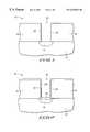
- FIG. 1is a diagrammatic sectional view of a semiconductor wafer fragment at one processing step in accordance with the invention.
- FIG. 2is a view of the FIG. 1 wafer fragment at a processing step subsequent to that shown by FIG. 1 .
- FIG. 3is a view of the FIG. 1 wafer fragment at a processing step subsequent to that shown by FIG. 2 .
- FIG. 4is a view of the FIG. 1 wafer fragment at a processing step subsequent to that shown by FIG. 3 .
- a semiconductor wafer fragmentis indicated generally with reference numeral 10 .
- Suchcomprises a bulk monocrystalline silicon substrate 12 having a conductively doped diffusion region 14 formed therein.
- the term “semiconductive substrate”is defined to mean any construction comprising semiconductive material, including, but not limited to, bulk semiconductive materials such as a semiconductive wafer (either alone or in assemblies comprising other materials thereon), and semiconductive material layers (either alone or in assemblies comprising other materials).
- substraterefers to any supporting structure, including, but not limited to, the semiconductive substrates described above.
- An insulative layer 16is formed over substrate 12 .
- Example materialsinclude borophosphosilicate glass, undoped SiO 2 , and Si 3 N 4 .
- An opening 18is formed in insulative material 16 to substrate 12 , and in this example to substrate region 14 with which electrical connection is desired. Alternate substrate regions are of course contemplated, such as outer surfaces of silicon comprising plugs, conductive metal or metal compound layers and the like.
- the substrate region with which electrical connection in accordance with the invention is to be madecomprises silicon, most preferably in an elemental form whether monocrystalline, polycrystalline or amorphous. Opening 18 has insulative sidewalls 20 .
- an elemental metal or metal alloy layer 22is deposited over sidewalls 20 .
- a preferred process for achieving the deposition of FIG. 2comprises forming a plasma from source gases comprising a metal tetrahalide (i.e., TiCl 4 ) and H 2 .
- Argon or other gasesmight be present, including a silicon comprising source gas, although silicon comprising source gases are preferably not utilized in this part of the process.
- Such plasma deposition processpreferably forms a much thinner portion of metal layer 22 over insulative sidewalls 20 than over the illustrated outer/upper surfaces of material 16 .
- An example and preferred thickness for that portion of layer 22 over sidewalls 20is from about 10 Angstroms to about 100 Angstroms. Less than 100 Angstroms is most preferred for maximizing the volume of silicide to be deposited within the remaining volume of opening 18 .
- Example processes for achieving the FIG. 2 depositionare as described in U.S. Pat. No. 5,173,327, which is hereby incorporated by reference.
- a specific example for achieving the deposition of FIG. 2includes TiCl 4 flow at 100 sccm, H 2 flow at 5000 sccm, Ar flow at 5000 sccm, RF Power at 500W, pressure at 5 Torr, and temperature at 650° C.
- the deposition conditionsare preferably chosen to be effective for the depositing titanium to form a titanium silicide region 24 from reaction with the silicon comprising substrate region, in this example at the base of the opening and thereby in electrical connection with region 14 .
- metal layer 22is formed in electrical connection with substrate region through metal compound region 24 .
- depositions at temperatures greater than or equal to about 500° C.will result in in situ formation of silicide with the substrate during deposition.
- the outer surfaces of metal layer 22 and metal silicide region 24are nitridized to transform at least the outer portions thereof into a metal nitride (not specifically designated in the figures).
- the nitridationis more preferably conducted to be sufficiently complete to transform all of that portion of metal layer 22 over insulative sidewalls 20 into a metal nitride, but only the outermost portions of silicide layer 24 to metal nitride to leave a suicide contact interface to region 14 .
- the nitridizingcomprises exposing the outer surfaces of metal layer 22 and metal silicide region 24 to a nitrogen atom containing plasma.
- a preferred exampleincludes a mixture of hydrogen and nitrogen which is ideally void of any separate titanium component (i.e., void of TiCl 4 ).
- a preferred specific example plasma treatmentis to utilize hydrogen in the form H 2 gas and nitrogen in the form of N 2 gas at a volumetric feed ratio to a plasma enhanced chemical vapor deposition (PECVD) reactor of N 2 to H 2 of from about 2.25:1 to about 4:1.
- PECVDplasma enhanced chemical vapor deposition
- Subatmospheric pressureof from 1 Torr to 10 Torr and a temperature of greater than or equal to about 600° C. are also preferred.
- An example RF plasma poweris 250 W for a single wafer reactor.
- the hydrogen and nitrogen provided for such preferred treatmentcan be from a single molecular gas, such as NH 3 .
- the abovecomprises but one example of coating insulative sidewalls 20 within opening 18 with an electrically conductive material.
- an electrically conductive materialcomprises a metal compound, although the coating could consist essentially of an elemental metal or metal alloy, or other conductive materials.
- a metal compoundis preferred, such as TiN to take advantage of its known adhesion and barrier properties. Further in some instances, such a layer can act as a barrier against corrosion by CVD chemistries which might be utilized to deposit a silicide layer subsequently.
- Metal compound layerscould also, of course, be provided within opening 18 to coat insulative sidewalls 20 by other manners, such as chemical vapor deposition and other techniques.
- a metal silicide layer 26is deposited over metal and/or metal nitride layer 22 substantially selectively relative to any exposed insulative material to fill the remaining volume of opening 18 with silicide.
- substantially selectivemeans a deposition ratio of at least 2:1
- a preferred processis low pressure chemical vapor deposition at a temperature of least 650° C. comprising metal tetrahalide and SiH 4 source gases.
- An example preferred metal tetrahalideis TiCl 4 .
- the silicon source gascan be organic and inorganic.
- Example inorganic source gasesinclude silane, disilane, etc.
- Example organic silicon source gasescomprise methlysilane and the like. H 2 , Ar, and other gases can also of course be added.
- the substantially selective depositionis preferably not plasma enhanced, which facilitates or enhances the selectivity.
- a preferred temperature range for the selective depositionis from 650° C. to 900° C., with a preferred pressure range being from 10 mTorr to 10 Torr.
- a specific exampleis at 775° C. and 200 mTorr.
- a specific example involving silane and TiCl 4 flowsincludes feeding pure TiCl 4 and a mixture of 10% by volume silane in a helium carrier gas.
- a preferred range of flow ratios of such gases of the silane mixture and TiCl 4is from 20:1 to 100:1 by volume, thus providing a ratio of the silicon comprising compound silane in a ratio of from 2:1 to 10:1 by volume as compared to TiCl 4 .
- a preferred specific exampleis a 5:1 ratio.
- the substantially selective capable depositingcan occur where there is exposed insulative material during such depositing, as well as if there were no exposed insulative material during the depositing.
- the deposition of FIG. 3might be conducted where there are other exposed insulative surfaces on the wafer displaced from the depicted fragment, or such would occur if layer 22 were removed outwardly of the outermost surface of insulative material layer 16 prior to the deposit of layer 26 (not shown).
- exemplary subsequent processingis depicted whereby layers 26 and 22 outwardly of the outermost surface of insulative material layer 16 have been removed or otherwise planarized back to form an isolated metal silicide comprising contact plug 30 within what was formerly opening 18 .
- Layers 26 and 22 outwardly of layer 16could alternately be patterned or utilized as a conductive device component. Such would include by way of example only, a conductive line, a capacitor plate or other conductive component of a device.
Landscapes
- Engineering & Computer Science (AREA)
- Physics & Mathematics (AREA)
- Condensed Matter Physics & Semiconductors (AREA)
- General Physics & Mathematics (AREA)
- Manufacturing & Machinery (AREA)
- Computer Hardware Design (AREA)
- Microelectronics & Electronic Packaging (AREA)
- Power Engineering (AREA)
- Plasma & Fusion (AREA)
- Electrodes Of Semiconductors (AREA)
- Internal Circuitry In Semiconductor Integrated Circuit Devices (AREA)
Abstract
Description
Claims (31)
Priority Applications (1)
| Application Number | Priority Date | Filing Date | Title |
|---|---|---|---|
| US09/260,233US6245674B1 (en) | 1999-03-01 | 1999-03-01 | Method of forming a metal silicide comprising contact over a substrate |
Applications Claiming Priority (1)
| Application Number | Priority Date | Filing Date | Title |
|---|---|---|---|
| US09/260,233US6245674B1 (en) | 1999-03-01 | 1999-03-01 | Method of forming a metal silicide comprising contact over a substrate |
Publications (1)
| Publication Number | Publication Date |
|---|---|
| US6245674B1true US6245674B1 (en) | 2001-06-12 |
Family
ID=22988334
Family Applications (1)
| Application Number | Title | Priority Date | Filing Date |
|---|---|---|---|
| US09/260,233Expired - LifetimeUS6245674B1 (en) | 1999-03-01 | 1999-03-01 | Method of forming a metal silicide comprising contact over a substrate |
Country Status (1)
| Country | Link |
|---|---|
| US (1) | US6245674B1 (en) |
Cited By (10)
| Publication number | Priority date | Publication date | Assignee | Title |
|---|---|---|---|---|
| US6365515B1 (en)* | 2000-08-28 | 2002-04-02 | Micron Technology, Inc. | Chemical vapor deposition process |
| US6531352B1 (en)* | 2000-08-31 | 2003-03-11 | Micron Technology, Inc. | Methods of forming conductive interconnects |
| US6627526B1 (en)* | 2000-09-21 | 2003-09-30 | Advanced Micro Devices, Inc. | Method for fabricating a conductive structure for a semiconductor device |
| US6730355B2 (en) | 2002-03-06 | 2004-05-04 | Micron Technology, Inc. | Chemical vapor deposition method of forming a material over at least two substrates |
| US6767823B2 (en)* | 2002-03-06 | 2004-07-27 | Micron Technology, Inc. | Plasma enhanced chemical vapor deposition method of forming titanium silicide comprising layers |
| US20080136040A1 (en)* | 2006-12-11 | 2008-06-12 | Samsung Electronics Co., Ltd. | Methods of Forming Electrical Interconnects Using Non-Uniformly Nitrified Metal Layers and Interconnects Formed Thereby |
| US9466530B2 (en)* | 2014-10-29 | 2016-10-11 | Globalfoundries Inc. | Methods of forming an improved via to contact interface by selective formation of a metal silicide capping layer |
| US9559059B2 (en) | 2014-10-29 | 2017-01-31 | Globalfoundries Inc. | Methods of forming an improved via to contact interface by selective formation of a conductive capping layer |
| US20230386915A1 (en)* | 2022-05-26 | 2023-11-30 | Taiwan Semiconductor Manufacturing Company, Ltd. | Method for forming a contact plug by bottom-up metal growth |
| US20240136227A1 (en)* | 2019-07-31 | 2024-04-25 | Taiwan Semiconductor Manufacturing Co., Ltd. | Barrier-Free Approach for Forming Contact Plugs |
Citations (17)
| Publication number | Priority date | Publication date | Assignee | Title |
|---|---|---|---|---|
| US5173327A (en) | 1991-06-18 | 1992-12-22 | Micron Technology, Inc. | LPCVD process for depositing titanium films for semiconductor devices |
| US5296404A (en) | 1990-10-24 | 1994-03-22 | Sumitomo Metal Industries, Ltd. | Method for forming a thin film for a semiconductor device |
| US5326404A (en) | 1991-12-19 | 1994-07-05 | Sony Corporation | Plasma processing apparatus |
| US5344792A (en)* | 1993-03-04 | 1994-09-06 | Micron Technology, Inc. | Pulsed plasma enhanced CVD of metal silicide conductive films such as TiSi2 |
| EP0631309A2 (en) | 1993-06-28 | 1994-12-28 | Kawasaki Steel Corporation | Semiconductor device with contact structure and method of manufacturing the same |
| WO1995034092A1 (en) | 1994-06-03 | 1995-12-14 | Materials Research Corporation | A method of nitridization of titanium thin films |
| US5496752A (en) | 1992-10-15 | 1996-03-05 | Fujitsu Limited | Method of manufacturing thin film transistors in a liquid crystal display apparatus |
| US5510146A (en) | 1991-07-16 | 1996-04-23 | Seiko Epson Corporation | CVD apparatus, method of forming semiconductor film, and method of fabricating thin-film semiconductor device |
| US5529937A (en) | 1993-07-27 | 1996-06-25 | Semiconductor Energy Laboratory Co., Ltd. | Process for fabricating thin film transistor |
| US5567243A (en) | 1994-06-03 | 1996-10-22 | Sony Corporation | Apparatus for producing thin films by low temperature plasma-enhanced chemical vapor deposition using a rotating susceptor reactor |
| US5670425A (en)* | 1995-11-09 | 1997-09-23 | Lsi Logic Corporation | Process for making integrated circuit structure comprising local area interconnects formed over semiconductor substrate by selective deposition on seed layer in patterned trench |
| US5766997A (en) | 1909-11-30 | 1998-06-16 | Nkk Corporation | Method of forming floating gate type non-volatile semiconductor memory device having silicided source and drain regions |
| US5846881A (en)* | 1995-12-28 | 1998-12-08 | Micron Technology, Inc. | Low cost DRAM metallization |
| US5926737A (en)* | 1997-08-19 | 1999-07-20 | Tokyo Electron Limited | Use of TiCl4 etchback process during integrated CVD-Ti/TiN wafer processing |
| US5930671A (en)* | 1997-10-20 | 1999-07-27 | Industrial Technology Research Institute | CVD titanium silicide for contract hole plugs |
| US5976976A (en)* | 1997-08-21 | 1999-11-02 | Micron Technology, Inc. | Method of forming titanium silicide and titanium by chemical vapor deposition |
| US5975912A (en)* | 1994-06-03 | 1999-11-02 | Materials Research Corporation | Low temperature plasma-enhanced formation of integrated circuits |
- 1999
- 1999-03-01USUS09/260,233patent/US6245674B1/ennot_activeExpired - Lifetime
Patent Citations (18)
| Publication number | Priority date | Publication date | Assignee | Title |
|---|---|---|---|---|
| US5766997A (en) | 1909-11-30 | 1998-06-16 | Nkk Corporation | Method of forming floating gate type non-volatile semiconductor memory device having silicided source and drain regions |
| US5296404A (en) | 1990-10-24 | 1994-03-22 | Sumitomo Metal Industries, Ltd. | Method for forming a thin film for a semiconductor device |
| US5173327A (en) | 1991-06-18 | 1992-12-22 | Micron Technology, Inc. | LPCVD process for depositing titanium films for semiconductor devices |
| US5510146A (en) | 1991-07-16 | 1996-04-23 | Seiko Epson Corporation | CVD apparatus, method of forming semiconductor film, and method of fabricating thin-film semiconductor device |
| US5326404A (en) | 1991-12-19 | 1994-07-05 | Sony Corporation | Plasma processing apparatus |
| US5496752A (en) | 1992-10-15 | 1996-03-05 | Fujitsu Limited | Method of manufacturing thin film transistors in a liquid crystal display apparatus |
| US5344792A (en)* | 1993-03-04 | 1994-09-06 | Micron Technology, Inc. | Pulsed plasma enhanced CVD of metal silicide conductive films such as TiSi2 |
| EP0631309A2 (en) | 1993-06-28 | 1994-12-28 | Kawasaki Steel Corporation | Semiconductor device with contact structure and method of manufacturing the same |
| US5529937A (en) | 1993-07-27 | 1996-06-25 | Semiconductor Energy Laboratory Co., Ltd. | Process for fabricating thin film transistor |
| US5567243A (en) | 1994-06-03 | 1996-10-22 | Sony Corporation | Apparatus for producing thin films by low temperature plasma-enhanced chemical vapor deposition using a rotating susceptor reactor |
| US5593511A (en) | 1994-06-03 | 1997-01-14 | Sony Corporation | Method of nitridization of titanium thin films |
| WO1995034092A1 (en) | 1994-06-03 | 1995-12-14 | Materials Research Corporation | A method of nitridization of titanium thin films |
| US5975912A (en)* | 1994-06-03 | 1999-11-02 | Materials Research Corporation | Low temperature plasma-enhanced formation of integrated circuits |
| US5670425A (en)* | 1995-11-09 | 1997-09-23 | Lsi Logic Corporation | Process for making integrated circuit structure comprising local area interconnects formed over semiconductor substrate by selective deposition on seed layer in patterned trench |
| US5846881A (en)* | 1995-12-28 | 1998-12-08 | Micron Technology, Inc. | Low cost DRAM metallization |
| US5926737A (en)* | 1997-08-19 | 1999-07-20 | Tokyo Electron Limited | Use of TiCl4 etchback process during integrated CVD-Ti/TiN wafer processing |
| US5976976A (en)* | 1997-08-21 | 1999-11-02 | Micron Technology, Inc. | Method of forming titanium silicide and titanium by chemical vapor deposition |
| US5930671A (en)* | 1997-10-20 | 1999-07-27 | Industrial Technology Research Institute | CVD titanium silicide for contract hole plugs |
Non-Patent Citations (2)
| Title |
|---|
| A Bouteville, J.C. Remy and C. Attuyt, "TiSi2 Selective Growth in a Rapid Thermal Low Pressure Chemical Vapor Deposition System", J. Electrochem Soc., vol. 139, No. 8, Aug. 1992. |
| Murakami, S, et al., "Plasma-Nitridated Ti Contact System for VLSI Interconnections", 4th Internat. IEEE VLSI Multilevel Interconnection Conference, Santa Clara CA, Jun. 15-16, 1987. |
Cited By (20)
| Publication number | Priority date | Publication date | Assignee | Title |
|---|---|---|---|---|
| US6472321B2 (en)* | 2000-08-28 | 2002-10-29 | Micron Technology, Inc. | Chemical vapor deposition process |
| US6365515B1 (en)* | 2000-08-28 | 2002-04-02 | Micron Technology, Inc. | Chemical vapor deposition process |
| US20040166622A1 (en)* | 2000-08-31 | 2004-08-26 | Sandhu Gurtej S. | Methods of forming conductive interconnects |
| US6531352B1 (en)* | 2000-08-31 | 2003-03-11 | Micron Technology, Inc. | Methods of forming conductive interconnects |
| US6750089B2 (en)* | 2000-08-31 | 2004-06-15 | Micron Technology, Inc. | Methods of forming conductive interconnects |
| US6800517B2 (en) | 2000-08-31 | 2004-10-05 | Micron Technology, Inc. | Methods of forming conductive interconnects |
| US6627526B1 (en)* | 2000-09-21 | 2003-09-30 | Advanced Micro Devices, Inc. | Method for fabricating a conductive structure for a semiconductor device |
| US7033642B2 (en)* | 2002-03-06 | 2006-04-25 | Micron Technology, Inc. | Plasma enhanced chemical vapor deposition method of forming a titanium silicide comprising layer |
| US6767823B2 (en)* | 2002-03-06 | 2004-07-27 | Micron Technology, Inc. | Plasma enhanced chemical vapor deposition method of forming titanium silicide comprising layers |
| US20050079697A1 (en)* | 2002-03-06 | 2005-04-14 | Cem Basceri | Plasma enhanced chemical vapor deposition method of forming a titanium silicide comprising layer |
| US6730355B2 (en) | 2002-03-06 | 2004-05-04 | Micron Technology, Inc. | Chemical vapor deposition method of forming a material over at least two substrates |
| US20060172088A1 (en)* | 2002-03-06 | 2006-08-03 | Cem Basceri | Plasma enhanced chemical vapor deposition method of forming titanium silicide comprising layers |
| US7393563B2 (en) | 2002-03-06 | 2008-07-01 | Micron Technology, Inc. | Plasma enhanced chemical vapor deposition method of forming titanium silicide comprising layers |
| US7396570B2 (en) | 2002-03-06 | 2008-07-08 | Micron Technology, Inc. | Plasma enhanced chemical vapor deposition method of forming titanium silicide comprising layers |
| US20080136040A1 (en)* | 2006-12-11 | 2008-06-12 | Samsung Electronics Co., Ltd. | Methods of Forming Electrical Interconnects Using Non-Uniformly Nitrified Metal Layers and Interconnects Formed Thereby |
| US9466530B2 (en)* | 2014-10-29 | 2016-10-11 | Globalfoundries Inc. | Methods of forming an improved via to contact interface by selective formation of a metal silicide capping layer |
| US9559059B2 (en) | 2014-10-29 | 2017-01-31 | Globalfoundries Inc. | Methods of forming an improved via to contact interface by selective formation of a conductive capping layer |
| US20240136227A1 (en)* | 2019-07-31 | 2024-04-25 | Taiwan Semiconductor Manufacturing Co., Ltd. | Barrier-Free Approach for Forming Contact Plugs |
| US20230386915A1 (en)* | 2022-05-26 | 2023-11-30 | Taiwan Semiconductor Manufacturing Company, Ltd. | Method for forming a contact plug by bottom-up metal growth |
| US12412781B2 (en)* | 2022-05-26 | 2025-09-09 | Taiwan Semiconductor Manufacturing Company, Ltd. | Method for forming a contact plug by bottom-up metal growth |
Similar Documents
| Publication | Publication Date | Title |
|---|---|---|
| US6830838B2 (en) | Chemical vapor deposition of titanium | |
| US5773363A (en) | Semiconductor processing method of making electrical contact to a node | |
| JP3358328B2 (en) | Method of forming high melting point metal film | |
| US6133147A (en) | Process for selective metal deposition in holes of semiconductor device | |
| US6067680A (en) | Semiconductor processing method of forming a conductively doped semiconductive material plug within a contact opening | |
| US20060246714A1 (en) | Method of forming a conductive contact | |
| US6136690A (en) | In situ plasma pre-deposition wafer treatment in chemical vapor deposition technology for semiconductor integrated circuit applications | |
| JPH09509288A (en) | Method for depositing tungsten nitride using silicon-containing source gas | |
| JP2002515649A (en) | Conformal layer multi-step formation method | |
| JPH09237838A (en) | Metal wiring structure and its formation | |
| US6696368B2 (en) | Titanium boronitride layer for high aspect ratio semiconductor devices | |
| US6245674B1 (en) | Method of forming a metal silicide comprising contact over a substrate | |
| US6368962B2 (en) | Semiconductor processing method of forming a conductive line, and buried bit line memory circuitry | |
| US5977636A (en) | Method of forming an electrically conductive contact plug, method of forming a reactive or diffusion barrier layer over a substrate, integrated circuitry, and method of forming a layer of titanium boride | |
| US6649518B2 (en) | Method of forming a conductive contact | |
| US6433434B1 (en) | Apparatus having a titanium alloy layer | |
| US5759905A (en) | Semiconductor processing method of forming a conductively doped semiconductive material plug within a contact opening | |
| KR100578221B1 (en) | Method for manufacturing semiconductor device having diffusion barrier | |
| WO1998043284A1 (en) | Titanium metal treatment method, method of forming an electrically conductive interconnect, and method of reducing contact resistance of an elemental titanium contact | |
| KR100275331B1 (en) | Metal wiring formation method of semiconductor device | |
| JPH053171A (en) | Forming method of tungsten plug | |
| KR20050067573A (en) | Fabricating method of small contact in semiconductor device | |
| KR20010064063A (en) | A method for forming metal wire in semicondutor device |
Legal Events
| Date | Code | Title | Description |
|---|---|---|---|
| AS | Assignment | Owner name:MICRON TECHNOLOGY, INC., IDAHO Free format text:ASSIGNMENT OF ASSIGNORS INTEREST;ASSIGNOR:SANDHU, GURTEJ S.;REEL/FRAME:009810/0862 Effective date:19990224 | |
| FEPP | Fee payment procedure | Free format text:PAYOR NUMBER ASSIGNED (ORIGINAL EVENT CODE: ASPN); ENTITY STATUS OF PATENT OWNER: LARGE ENTITY | |
| STCF | Information on status: patent grant | Free format text:PATENTED CASE | |
| CC | Certificate of correction | ||
| FPAY | Fee payment | Year of fee payment:4 | |
| FPAY | Fee payment | Year of fee payment:8 | |
| FPAY | Fee payment | Year of fee payment:12 | |
| AS | Assignment | Owner name:U.S. BANK NATIONAL ASSOCIATION, AS COLLATERAL AGENT, CALIFORNIA Free format text:SECURITY INTEREST;ASSIGNOR:MICRON TECHNOLOGY, INC.;REEL/FRAME:038669/0001 Effective date:20160426 Owner name:U.S. BANK NATIONAL ASSOCIATION, AS COLLATERAL AGEN Free format text:SECURITY INTEREST;ASSIGNOR:MICRON TECHNOLOGY, INC.;REEL/FRAME:038669/0001 Effective date:20160426 | |
| AS | Assignment | Owner name:MORGAN STANLEY SENIOR FUNDING, INC., AS COLLATERAL AGENT, MARYLAND Free format text:PATENT SECURITY AGREEMENT;ASSIGNOR:MICRON TECHNOLOGY, INC.;REEL/FRAME:038954/0001 Effective date:20160426 Owner name:MORGAN STANLEY SENIOR FUNDING, INC., AS COLLATERAL Free format text:PATENT SECURITY AGREEMENT;ASSIGNOR:MICRON TECHNOLOGY, INC.;REEL/FRAME:038954/0001 Effective date:20160426 | |
| AS | Assignment | Owner name:U.S. BANK NATIONAL ASSOCIATION, AS COLLATERAL AGENT, CALIFORNIA Free format text:CORRECTIVE ASSIGNMENT TO CORRECT THE REPLACE ERRONEOUSLY FILED PATENT #7358718 WITH THE CORRECT PATENT #7358178 PREVIOUSLY RECORDED ON REEL 038669 FRAME 0001. ASSIGNOR(S) HEREBY CONFIRMS THE SECURITY INTEREST;ASSIGNOR:MICRON TECHNOLOGY, INC.;REEL/FRAME:043079/0001 Effective date:20160426 Owner name:U.S. BANK NATIONAL ASSOCIATION, AS COLLATERAL AGEN Free format text:CORRECTIVE ASSIGNMENT TO CORRECT THE REPLACE ERRONEOUSLY FILED PATENT #7358718 WITH THE CORRECT PATENT #7358178 PREVIOUSLY RECORDED ON REEL 038669 FRAME 0001. ASSIGNOR(S) HEREBY CONFIRMS THE SECURITY INTEREST;ASSIGNOR:MICRON TECHNOLOGY, INC.;REEL/FRAME:043079/0001 Effective date:20160426 | |
| AS | Assignment | Owner name:JPMORGAN CHASE BANK, N.A., AS COLLATERAL AGENT, ILLINOIS Free format text:SECURITY INTEREST;ASSIGNORS:MICRON TECHNOLOGY, INC.;MICRON SEMICONDUCTOR PRODUCTS, INC.;REEL/FRAME:047540/0001 Effective date:20180703 Owner name:JPMORGAN CHASE BANK, N.A., AS COLLATERAL AGENT, IL Free format text:SECURITY INTEREST;ASSIGNORS:MICRON TECHNOLOGY, INC.;MICRON SEMICONDUCTOR PRODUCTS, INC.;REEL/FRAME:047540/0001 Effective date:20180703 | |
| AS | Assignment | Owner name:MICRON TECHNOLOGY, INC., IDAHO Free format text:RELEASE BY SECURED PARTY;ASSIGNOR:U.S. BANK NATIONAL ASSOCIATION, AS COLLATERAL AGENT;REEL/FRAME:047243/0001 Effective date:20180629 | |
| AS | Assignment | Owner name:MICRON TECHNOLOGY, INC., IDAHO Free format text:RELEASE BY SECURED PARTY;ASSIGNOR:MORGAN STANLEY SENIOR FUNDING, INC., AS COLLATERAL AGENT;REEL/FRAME:050937/0001 Effective date:20190731 | |
| AS | Assignment | Owner name:MICRON SEMICONDUCTOR PRODUCTS, INC., IDAHO Free format text:RELEASE BY SECURED PARTY;ASSIGNOR:JPMORGAN CHASE BANK, N.A., AS COLLATERAL AGENT;REEL/FRAME:051028/0001 Effective date:20190731 Owner name:MICRON TECHNOLOGY, INC., IDAHO Free format text:RELEASE BY SECURED PARTY;ASSIGNOR:JPMORGAN CHASE BANK, N.A., AS COLLATERAL AGENT;REEL/FRAME:051028/0001 Effective date:20190731 |