US6243566B1 - Impedance matching for a dual band power amplifier - Google Patents
Impedance matching for a dual band power amplifierDownload PDFInfo
- Publication number
- US6243566B1 US6243566B1US09/562,734US56273400AUS6243566B1US 6243566 B1US6243566 B1US 6243566B1US 56273400 AUS56273400 AUS 56273400AUS 6243566 B1US6243566 B1US 6243566B1
- Authority
- US
- United States
- Prior art keywords
- matching circuit
- transmission line
- power amplifier
- mhz
- frequency band
- Prior art date
- Legal status (The legal status is an assumption and is not a legal conclusion. Google has not performed a legal analysis and makes no representation as to the accuracy of the status listed.)
- Expired - Lifetime
Links
Images


Classifications
- H—ELECTRICITY
- H03—ELECTRONIC CIRCUITRY
- H03F—AMPLIFIERS
- H03F1/00—Details of amplifiers with only discharge tubes, only semiconductor devices or only unspecified devices as amplifying elements
- H03F1/56—Modifications of input or output impedances, not otherwise provided for
- H—ELECTRICITY
- H04—ELECTRIC COMMUNICATION TECHNIQUE
- H04B—TRANSMISSION
- H04B1/00—Details of transmission systems, not covered by a single one of groups H04B3/00 - H04B13/00; Details of transmission systems not characterised by the medium used for transmission
- H04B1/005—Details of transmission systems, not covered by a single one of groups H04B3/00 - H04B13/00; Details of transmission systems not characterised by the medium used for transmission adapting radio receivers, transmitters andtransceivers for operation on two or more bands, i.e. frequency ranges
- H—ELECTRICITY
- H04—ELECTRIC COMMUNICATION TECHNIQUE
- H04B—TRANSMISSION
- H04B1/00—Details of transmission systems, not covered by a single one of groups H04B3/00 - H04B13/00; Details of transmission systems not characterised by the medium used for transmission
- H04B1/02—Transmitters
- H04B1/04—Circuits
- H04B1/0458—Arrangements for matching and coupling between power amplifier and antenna or between amplifying stages
- H—ELECTRICITY
- H04—ELECTRIC COMMUNICATION TECHNIQUE
- H04B—TRANSMISSION
- H04B1/00—Details of transmission systems, not covered by a single one of groups H04B3/00 - H04B13/00; Details of transmission systems not characterised by the medium used for transmission
- H04B1/38—Transceivers, i.e. devices in which transmitter and receiver form a structural unit and in which at least one part is used for functions of transmitting and receiving
- H04B1/40—Circuits
- H04B1/403—Circuits using the same oscillator for generating both the transmitter frequency and the receiver local oscillator frequency
- H04B1/406—Circuits using the same oscillator for generating both the transmitter frequency and the receiver local oscillator frequency with more than one transmission mode, e.g. analog and digital modes
- H—ELECTRICITY
- H04—ELECTRIC COMMUNICATION TECHNIQUE
- H04B—TRANSMISSION
- H04B1/00—Details of transmission systems, not covered by a single one of groups H04B3/00 - H04B13/00; Details of transmission systems not characterised by the medium used for transmission
- H—ELECTRICITY
- H04—ELECTRIC COMMUNICATION TECHNIQUE
- H04B—TRANSMISSION
- H04B1/00—Details of transmission systems, not covered by a single one of groups H04B3/00 - H04B13/00; Details of transmission systems not characterised by the medium used for transmission
- H04B1/02—Transmitters
- H04B1/04—Circuits
Definitions
- This inventionrelates generally to dual band communication systems, and more particularly to impedance matching circuits for a power amplifier in a dual band transmitter.
- a dual mode transmittercan operate using two different systems.
- an AM/FM dual mode transmittercan transmit both amplitude modulated and frequency modulated signals.
- a dual band transmittercan operate using two different cellular telephone systems.
- GSMGlobal System for Mobile Communications
- DCSDigital Communications System
- the power amplifier at the final stage of the transmittershould be matched to the impedance of the antenna. Additionally, harmonics of the transmitted frequency band should be suppressed to reduce interference with other communication systems operating at the harmonic frequencies. With a GSM/DCS dual band transmitter, it is difficult to suppress the first (1800) MHz harmonic during 900 MHz GSM transmissions and yet pass the 1800 MHz signal during DCS transmissions. Also the output impedance of a radiotelephone power amplifier should be matched to the antenna so that the impedance at the output of the amplifier is at the optimum impedance for power efficient amplification.
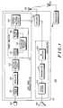
- FIG. 1shows a diagram of a communication system having matching circuits according to a preferred embodiment.
- FIG. 2shows a diagram of the exciter matching circuit according to the preferred embodiment.
- FIG. 3shows a diagram of the two-stage power amplifier according to the preferred embodiment.
- FIG. 4shows a diagram of the harmonic filter matching circuit according to the preferred embodiment.
- FIG. 5shows a graph of a return loss signal and an attenuation signal at the output of the harmonic filter matching circuit in GSM mode according to the preferred embodiment.
- FIG. 6shows a graph of a return loss signal and an attenuation signal at the output of the harmonic filter matching circuit in DCS mode according to the preferred embodiment.
- Three matching circuitsenable a modulator, power amplifier, and antenna of a radiotelephone transmitter to efficiently amplify and transmit signals at more than one frequency band while suppressing first, second, and higher order harmonics.
- An exciter matching circuitmatches the impedance at the output of the modulator to the impedance at the input of the power amplifier for both modes of a dual band transmitter.
- An interstage matching circuithas a switch to match impedances between a first stage and a second stage of a power amplifier during different bands of operation.
- a harmonic filter matching circuituses a switch to match impedances and adjust the filter pass band of a combined filter and matching circuit during different modes of operation.
- FIG. 1shows a diagram of a communication system 100 having matching circuits 125 , 134 , 140 according to a preferred embodiment.
- the communication system 100 shownis a cellular communication system with a handset radiotelephone 101 and a base station transceiver 190 , however, a different communication system could be substituted, such as a modulator/demodulator (MODEM), a paging system, or a two-way radio system.
- the radiotelephone 101is a dual band GSM/DCS radiotelephone, however, other transmission modes with constant envelope modulation schemes can be substituted for either the GSM mode, the DCS mode, or both modes.
- AMPSAdvanced Mobile Phone Service
- ETACSEuropean Total Access Cellular System
- FMfrequency modulation
- PCSPersonal Communication System
- GSMGaussian Minimum Shift Keying
- Transmission modesmay also be added to create a tri-mode or quad-mode radiotelephone.
- the radiotelephone 101includes a microphone 105 for picking up audio signals.
- the audio signalsare coded by a speech coder 115 and sent to a modulator 120 .
- the modulator 120mixes the coded signals to 900 MHz in the case of GSM or 1800 MHz in the case of DCS.
- An exciter matching circuit 125includes a bipolar junction transistor (BJT) and matches the approximately 50 ⁇ impedance at the BJT output to the approximately 7 ⁇ impedance at the power amplifier 130 input for the frequency bands of interest, which is either at 900 MHz or 1800 MHz depending on the mode in use.
- BJTbipolar junction transistor
- Power amplifier 130is preferably a gallium arsenide (GaAs) field-effect transistor (FET) two-stage amplifier with a first stage 132 and a second stage 136 .
- GaAsgallium arsenide
- FETfield-effect transistor
- Other device types, however, such as silicon BJTs or silicon FETscould be substituted for the GaAs FETs.
- interstage matching circuit 134that optimizes the impedance matching at either 900 MHz or 1800 MHz depending on the mode in use.
- a harmonic filter matching circuit 140matches the outgoing signal to the approximately 50 ⁇ antenna 155 at the frequency band of interest and filters out first, second, and higher order harmonics of the signal.
- the matched impedances presented to the power amplifer input and the power amplifier output by the exciter matching circuit 125 and the harmonic filter matching circuit 140determine the efficiency of the power amplifier.
- the transmitted signalis received by a complementary transceiver 190 , such as a GSM cellular base station, through an antenna 195 .
- a DCS base stationis also compatible with the GSM/DCS radiotelephone 101 , and other transceivers would be compatible with PCS, AMPS, or ETACS dual mode radiotelephones.
- Signals from the base station transceiver 190are transmitted from the antenna 195 of the base station and received by the antenna 155 of the radiotelephone 101 .
- a duplexer 150 in the radiotelephone 101controls whether the antenna 155 is transmitting or receiving signals. Received signals are sent through the duplexer 150 to receiver 160 .
- a radio frequency (RF) receiver 165prepares the signal for demodulation, a demodulator 170 demodulates the signal, and a speech decoder 175 decodes the demodulated signal to an audio format for reproduction on speaker 180 .
- RFradio frequency
- FIG. 2shows a diagram of the exciter matching circuit 125 according to the preferred embodiment.
- a GSM signal at 900 MHzemerges from the modulator 120 (shown in FIG. 1 )
- certain components of the exciter matching circuit 125dominate the impedance response to promote a match to the power amplifier (shown in FIG. 1) at 900 MHz while rejecting other frequencies.
- a DCS signal at 1800 MHzcomes from the modulator 120
- different componentsdominate the impedance response of the exciter matching circuit 125 to create a good match at 1800 MHz while creating a poor match at other frequencies.
- the modulator 120is isolated from the power amplifier 130 (shown in FIG. 1) using a resistance buffer with resistor 205 and resistor 207 .
- a 1 pF capacitance 215is also connected from ground to the base of a BJT 210 .
- the BJT 210is used to amplify and transform the impedance of a modulated signal before the signal enters the power amplifier 130 (shown in FIG. 1 ).
- the output of the BJTis at approximately 50 ⁇ .
- a quarter-wave transmission line 220is connected from the collector of the BJT 210 to a constant voltage source V B2 . This transmission line 220 acts as an inductor when the modulated signal is at 900 MHz and acts as an open circuit when the modulated signal is at 1800 MHz.
- a 68 pF capacitance 225is connected between the voltage source V B2 and ground, and a resistor 227 is parallel to the transmission line 220 .
- the resistor 227stabilizes the BJT by providing a resistive termination when the transmission line 220 acts at an open circuit.
- a 4.7 pF capacitance 230is also connected to the collector of the BJT 210 , which functions as a direct current (DC) blocking element and as an impedance transforming element at 900 MHz.
- Two transmission lines 240 , 250connect the signal from the capacitance 230 to the output of the exciter matching circuit 125 , which connects to the power amplifier 130 (shown in FIG. 1 ). Between the two transmission lines 240 , 250 is a 1.5 pF capacitance 245 to ground.
- the inductance of the transmission line 220 and capacitance 230dominate the impedance of the exciter matching circuit 125 to create a good match at 900 MHz at approximately 7 ⁇ input impedance of the power amplifier 130 (shown in FIG. 1 ).
- the other elements in the exciter matching circuit 125have a negligible effect on the impedance at the 1800 MHz frequency band.
- the inductance of the transmission line 220 and the capacitance 230act as a high pass filter that also transforms lower frequency signals.
- the transmission line 220When an 1800 MHz DCS modulated signal enters the exciter matching circuit 125 , the transmission line 220 is open and the inductance of transmission lines 240 , 250 and the capacitance 245 dominate the impedance of the exciter matching circuit 125 to create a good match at 1800 MHz to the approximately 7 ⁇ input impedance of the power amplifier 130 (shown in FIG. 1 ). In this case, the transmission line 220 and capacitance 230 have a negligible effect on the impedance at the 900 MHz frequency band.
- the inductance of the transmission lines 240 , 250 and the capacitance 245act as a low pass filter that also transforms higher frequency signals.
- FIG. 3shows a diagram of the two-stage power amplifier 130 according to the preferred embodiment.
- An interstage matching circuit 134matches the impedances between the first stage 132 and the second stage 136 of the two-stage power amplifier 130 .
- the interstage matching circuit 134optimizes the impedances at 900 MHz or 1800 MHz depending on which transmission mode is in use.
- MESFETsTwo metal semiconductor field-effect transistors
- Alternatives to the MESFETsinclude silicon BJTs, silicon MOSFETs, and heterojunction bipolar transistors (HBTs).
- HBTsheterojunction bipolar transistors
- Between the two stages 132 , 136is a 15 pF capacitance 325 , and at the source of the first stage 132 is a small 3 nH inductance 335 which is connected to a voltage source V B3 .
- the two stages 132 , 136 , the inductance 335 , and the capacitance 325are integrated onto a chip 310 .
- a 2.7 pF capacitance 340is connected between the inductance 335 and the voltage source V B3 .
- a 1000 pF capacitance 350is also connected to the voltage source V B3 with a diode 370 connected from the capacitance 350 to ground.
- a 1.5 k ⁇ resistor 360 with an input node 365is connected between the capacitance 350 and the diode 370 .
- the diode 370turns on and the 1000 pF capacitance 350 dominates the impedance of the interstage matching circuit 134 .
- the capacitance valuesare calculated so that 900 MHz GSM signals from the first stage 132 of the power amplifier 130 are matched to the second stage of the power amplifier 130 (shown in FIG. 1) when the input node 365 is connected to a 2.7 V positive voltage source.
- the voltage source applied to node 365is a GSM/DCS mode selection voltage. Voltage is applied to node 365 when the radiotelephone 101 is in GSM mode, and voltage is not applied to node 365 when the radiotelephone 101 is in DCS mode.
- FIG. 4shows a diagram of the harmonic filter matching circuit 140 according to the preferred embodiment.
- the harmonic filter matching circuit 140uses both impedance matching and low pass filtering to pass 900 MHz signals and suppress 1800 MHz, 2700 MHz, 3600 MHz, and higher order harmonics during GSM mode transmissions while passing 1800 MHz signals and suppressing 2700 MHz signals and 3600 MHz and higher order harmonics during DCS transmissions.
- Transmission line 410is preferably a half-wave transmission line at 2700 MHz.
- a 100 pF capacitance 412is also connected to the voltage source V B4 .
- a set of transmission lines 420 , 430 , 440 , 450is connected in series to the output of the power amplifier 130 .
- At the ends of each transmission lineis a connection from an approximately 3 pF capacitance 422 , 442 , 452 , 482 through a diode 415 , 425 , 435 , 445 to ground.
- the capacitance of each diode 415 , 425 , 435 , 445 when the diode is offadds a fixed parallel capacitance to the switched capacitances 422 , 442 , 452 , 483 .
- An additional 1.8 pF capacitance 432is connected in parallel to the first capacitance 422 and diode 415 pair.
- This structurecan be described as a cascade of four low-pass matching sections.
- the reactance of the first three sectionswhich include transmission lines 420 , 430 , 440 , are switchable using diodes 415 , 425 , 435 , 435 .
- Between each capacitance and diode pairis a 1.5 k ⁇ resistor 416 , 426 , 436 , 446 connected to node 465 , which controls the switching of the first three sections.
- a 100 pF capacitance 434connects the node 465 and ground.
- Additional 1 pF or less capacitances 462 , 472 , 492 , 414 , 424provide attenuation for the 2700 MHz, 3600 MHz and high order harmonics of the 900 MHz GSM and 1800 MHz DCS signals.
- the reactance of the final section, which includes transmission line 450is fixed. This final section suppresses 3600 MHz harmonics generated by the diodes 415 , 425 , 435 , 435 when they are off.
- the GSM/DCS mode selection voltage used for the interstage matching circuit 134can also be used to control the operation of the harmonic filter matching circuit 140 .
- Positive voltageis applied to node 465 when the radiotelephone 101 is in GSM mode, and negative, zero, or floating voltage is applied to node 465 when the radiotelephone 101 is in DCS mode.
- the operation of the harmonic filter matching circuit 140provides impedance matching at 900 MHz when the GSM mode is selected via node 465 with signal attenuation at the harmonic frequencies of 1800 MHz, 2700 MHz, and 3600 MHz as well as other high order harmonic frequencies.
- the harmonic filtermatches at 1800 MHz and provides signal attenuation starting at 2700 MHz as well as 3600 MHz and higher order harmonics.
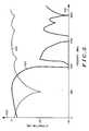
- FIG. 5shows a graph of a return loss signal 540 and an attenuation signal 550 at the output of the harmonic filter matching circuit 140 (shown in FIG. 1) in GSM mode according to the preferred embodiment.
- the X-axis 510 of the graphmeasures frequency in MHz while the Y-axis 520 of the graph measures attenuation in dB.
- the return loss signal 540has a significant lowering in return loss signal at 900 MHz, which indicates a good impedance match at the 900 MHz GSM frequency band.
- the attenuation signal 550is close to 0 dB, which passes the 900 MHz signal at full power. Meanwhile, at 1800 MHz, 2700 MHz, and 3600 MHz, the attenuation signal 550 lowers to dampen harmonics of the 900 MHz signal.
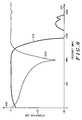
- FIG. 6shows a graph of a return loss signal 640 and an attenuation signal 650 at the output of the harmonic filter matching circuit 140 (shown in FIG. 1) in DCS mode according to the preferred embodiment.
- the X-axis 610 of the graphmeasures frequency in MHz while the Y-axis 620 measures attenuation in dB.
- the return loss signal 640has a significant lowering in return loss signal at 1800 MHz, which indicates a good impedance match at the 1800 MHz DCS frequency band.
- the attenuation signal 650is close to 0 dB, which is very different than the attenuation signal characteristic for the harmonic filter matching circuit when it is in the GSM mode.
- the attenuation signal 650still lowers at 2700 MHz and 3600 MHz to dampen harmonics of the 1800 MHz signal.
- component values of the exciter matching circuit 125 , the interstage matching circuit 134 , and the harmonic filter matching circuit 140can be adjusted to match only at the frequency bands of interest.
- transmission lines within the three matching circuitscan be replaced with inductances to reduce size or to promote fabrication onto an integrated circuit.
- the exciter matching circuituses impedance characteristics to promote matching of the modulator output and the power amplifier input of a dual mode transmitter at more than one frequency band of interest.
- the matching characteristics within the exciter matching circuitchange depending on the frequency band of the input signal.
- the interstage matching circuit 134uses a switch to add components, which varies the matching characteristic of the interstage matching circuit between the first stage and the second stage of a two-stage power amplifier depending on the mode used by the dual mode transmitter.
- the harmonic filter matching circuit 140also uses switches to add components to vary the matching characteristic and the filter characteristic of the harmonic filter matching circuit between the output of the power amplifier and the input of the antenna depending on the mode used by the dual mode transmitter.
- the three matching circuitsuse very few additional components to provide matching at more than one frequency band of interest and filter out undesired harmonics for dual mode transmitters dependent upon the mode in use. While specific components and functions of the impedance matching for a dual band power amplifier are described above, fewer or additional functions could be employed by one skilled in the art within the true spirit and scope of the present invention. The invention should be limited only by the appended claims.
Landscapes
- Engineering & Computer Science (AREA)
- Computer Networks & Wireless Communication (AREA)
- Signal Processing (AREA)
- Power Engineering (AREA)
- Transmitters (AREA)
- Amplifiers (AREA)
Abstract
Description
Claims (9)
Priority Applications (1)
| Application Number | Priority Date | Filing Date | Title |
|---|---|---|---|
| US09/562,734US6243566B1 (en) | 1997-02-19 | 2000-05-01 | Impedance matching for a dual band power amplifier |
Applications Claiming Priority (2)
| Application Number | Priority Date | Filing Date | Title |
|---|---|---|---|
| US08/802,831US6078794A (en) | 1997-02-19 | 1997-02-19 | Impedance matching for a dual band power amplifier |
| US09/562,734US6243566B1 (en) | 1997-02-19 | 2000-05-01 | Impedance matching for a dual band power amplifier |
Related Parent Applications (1)
| Application Number | Title | Priority Date | Filing Date |
|---|---|---|---|
| US08/802,831DivisionUS6078794A (en) | 1997-02-19 | 1997-02-19 | Impedance matching for a dual band power amplifier |
Publications (1)
| Publication Number | Publication Date |
|---|---|
| US6243566B1true US6243566B1 (en) | 2001-06-05 |
Family
ID=25184830
Family Applications (4)
| Application Number | Title | Priority Date | Filing Date |
|---|---|---|---|
| US08/802,831Expired - LifetimeUS6078794A (en) | 1997-02-19 | 1997-02-19 | Impedance matching for a dual band power amplifier |
| US09/562,734Expired - LifetimeUS6243566B1 (en) | 1997-02-19 | 2000-05-01 | Impedance matching for a dual band power amplifier |
| US09/563,721Expired - LifetimeUS6215359B1 (en) | 1997-02-19 | 2000-05-01 | Impedance matching for a dual band power amplifier |
| US09/562,733Expired - LifetimeUS6195536B1 (en) | 1997-02-19 | 2000-05-01 | Impedance matching for a dual band power amplifier |
Family Applications Before (1)
| Application Number | Title | Priority Date | Filing Date |
|---|---|---|---|
| US08/802,831Expired - LifetimeUS6078794A (en) | 1997-02-19 | 1997-02-19 | Impedance matching for a dual band power amplifier |
Family Applications After (2)
| Application Number | Title | Priority Date | Filing Date |
|---|---|---|---|
| US09/563,721Expired - LifetimeUS6215359B1 (en) | 1997-02-19 | 2000-05-01 | Impedance matching for a dual band power amplifier |
| US09/562,733Expired - LifetimeUS6195536B1 (en) | 1997-02-19 | 2000-05-01 | Impedance matching for a dual band power amplifier |
Country Status (4)
| Country | Link |
|---|---|
| US (4) | US6078794A (en) |
| CN (1) | CN1095251C (en) |
| FR (1) | FR2759823B1 (en) |
| GB (1) | GB2322493B (en) |
Cited By (14)
| Publication number | Priority date | Publication date | Assignee | Title |
|---|---|---|---|---|
| US6317608B1 (en)* | 1998-05-22 | 2001-11-13 | Telefonaktiebolaget Lm Ericsson | Power amplifier matching in dual band mobile phone |
| US20020125946A1 (en)* | 2001-03-12 | 2002-09-12 | Alps Electric Co., Ltd. | Miniaturized buffer amplifier and electronic circuit unit using same |
| US20030092388A1 (en)* | 2001-11-14 | 2003-05-15 | Koninklijke Philips Electronics N.V. | Impedeance matching circuit for a multi-band radio frequency device |
| US20040008082A1 (en)* | 2002-07-09 | 2004-01-15 | Dow Gee Samuel | Power amplifier with load switching circuit |
| US6741140B2 (en)* | 2001-12-12 | 2004-05-25 | Nortel Networks Limited | Circuit for receiving an AC coupled broadband signal |
| US20040121745A1 (en)* | 2001-08-29 | 2004-06-24 | Meck Ronald A. | Method and apparatus for impedance matching in an amplifier using lumped and distributed inductance |
| US6882836B2 (en) | 2002-07-16 | 2005-04-19 | Ericsson, Inc. | GAIT antenna interface with special isolation mode |
| US20070018758A1 (en)* | 2003-03-14 | 2007-01-25 | Ntt Docomo Inc. | Matching circuit |
| CN1307791C (en)* | 2002-01-15 | 2007-03-28 | M/A-Com尤罗泰克公司 | Switchable Power Amplifier |
| US20080026709A1 (en)* | 2006-07-28 | 2008-01-31 | Lianjun Liu | Re-configurable impedance matching and harmonic filter system |
| US20100184371A1 (en)* | 2008-09-17 | 2010-07-22 | Qualcomm Incorporated | Transmitters for wireless power transmission |
| US20100190435A1 (en)* | 2008-08-25 | 2010-07-29 | Qualcomm Incorporated | Passive receivers for wireless power transmission |
| US20130107914A1 (en)* | 2011-06-08 | 2013-05-02 | Bongseok Park | Antenna Tuning Using the Ratio of Complex Forward and Reflected Signals |
| US8947041B2 (en) | 2008-09-02 | 2015-02-03 | Qualcomm Incorporated | Bidirectional wireless power transmission |
Families Citing this family (50)
| Publication number | Priority date | Publication date | Assignee | Title |
|---|---|---|---|---|
| US6078794A (en)* | 1997-02-19 | 2000-06-20 | Motorola, Inc. | Impedance matching for a dual band power amplifier |
| KR100247013B1 (en)* | 1997-12-19 | 2000-03-15 | 윤종용 | Power control unit of radio transmitter |
| US6304748B1 (en)* | 1998-09-23 | 2001-10-16 | Conexant Systems, Inc. | Transmitter circuitry for a cellular phone |
| EP1035657B1 (en)* | 1999-03-08 | 2002-12-18 | Motorola, Inc. | Transmitter |
| FI990687L (en)* | 1999-03-29 | 2000-09-30 | Nokia Mobile Phones Ltd | Wireless communication antenna matching system |
| AU5401499A (en)* | 1999-10-14 | 2001-04-26 | Alcatel | ADSL filter |
| US6281748B1 (en)* | 2000-01-14 | 2001-08-28 | Motorola, Inc. | Method of and apparatus for modulation dependent signal amplification |
| JP4679686B2 (en)* | 2000-02-07 | 2011-04-27 | パナソニック株式会社 | Wireless communication apparatus and transmission power control method |
| US6625470B1 (en) | 2000-03-02 | 2003-09-23 | Motorola, Inc. | Transmitter |
| JP2002064386A (en)* | 2000-08-23 | 2002-02-28 | Sony Corp | Matching device |
| JP3733115B2 (en)* | 2000-09-18 | 2006-01-11 | インターナショナル・レクチファイヤー・コーポレーション | Current detection IC |
| US6489862B1 (en)* | 2000-10-03 | 2002-12-03 | Agilent Technologies, Inc. | Method for reducing noise generated in a power amplifier |
| US7006553B1 (en)* | 2000-10-10 | 2006-02-28 | Freescale Semiconductor, Inc. | Analog signal separator for UWB versus narrowband signals |
| JP2002280911A (en) | 2001-03-19 | 2002-09-27 | Nec Corp | Transmission circuit and communication terminal having the same mounted thereon |
| US6650200B2 (en) | 2001-04-20 | 2003-11-18 | Anaren Microwave, Inc. | Dynamic combiner/splitter for RF signal systems |
| GB2376823B (en)* | 2001-06-20 | 2005-05-18 | Ericsson Telefon Ab L M | Communications device |
| EP1296452A1 (en) | 2001-09-20 | 2003-03-26 | SMARTEQ Wireless AB | A radio antenna matching circuit |
| US6819941B2 (en) | 2001-10-11 | 2004-11-16 | Rf Micro Devices, Inc. | Single output stage power amplification for multimode applications |
| DE10233775B4 (en)* | 2002-07-25 | 2009-10-08 | Telefonaktiebolaget Lm Ericsson (Publ) | Method for dimensioning a matching element in the transmission branch of a mobile device |
| US7187231B2 (en)* | 2002-12-02 | 2007-03-06 | M/A-Com, Inc. | Apparatus, methods and articles of manufacture for multiband signal processing |
| FI114057B (en)* | 2002-10-18 | 2004-07-30 | Nokia Corp | A method and arrangement for detecting a load mismatch, and a radio device using such |
| EP1450486A1 (en)* | 2003-02-20 | 2004-08-25 | TDK Corporation | Multi-Mode Filter |
| JP2005124126A (en)* | 2003-09-24 | 2005-05-12 | Seiko Epson Corp | Impedance circuit network, filter circuit using the same, amplifier circuit, semiconductor integrated circuit, electronic device, and wireless communication device |
| US7343138B2 (en)* | 2003-12-08 | 2008-03-11 | M/A-Com, Inc. | Compensating for load pull in electromagentic signal propagation using adaptive impedance matching |
| US7660562B2 (en)* | 2004-06-21 | 2010-02-09 | M/A-Com Technology Solutions Holdings, Inc. | Combined matching and filter circuit |
| CN1977467B (en)* | 2004-06-30 | 2010-05-05 | 日立金属株式会社 | High frequency component and multi-band communication apparatus |
| US20060170492A1 (en)* | 2005-02-02 | 2006-08-03 | Chang Sheng-Fuh | Dual-band power amplifier |
| US7193477B2 (en)* | 2005-06-08 | 2007-03-20 | Integrated System Solution Corp. | Concurrent triple-band gain amplifier for multi-standard coexist communications |
| US20070218856A1 (en)* | 2006-03-17 | 2007-09-20 | Sami Vilhonen | Receiver, transceiver and receiving method |
| US7796953B2 (en)* | 2006-03-17 | 2010-09-14 | Nokia Corporation | Transmitter, power amplifier and filtering method |
| JP5079387B2 (en)* | 2007-05-10 | 2012-11-21 | 株式会社エヌ・ティ・ティ・ドコモ | Matching circuit |
| US7932782B2 (en)* | 2007-12-10 | 2011-04-26 | City University Of Hong Kong | Average power efficiency enhancement and linearity improvement of microwave power amplifiers |
| US8170505B2 (en)* | 2008-07-30 | 2012-05-01 | Qualcomm Incorporated | Driver amplifier having a programmable output impedance adjustment circuit |
| US9143172B2 (en)* | 2009-06-03 | 2015-09-22 | Qualcomm Incorporated | Tunable matching circuits for power amplifiers |
| US8963611B2 (en)* | 2009-06-19 | 2015-02-24 | Qualcomm Incorporated | Power and impedance measurement circuits for a wireless communication device |
| US8750810B2 (en)* | 2009-07-24 | 2014-06-10 | Qualcomm Incorporated | Power amplifier with switched output matching for multi-mode operation |
| US8072272B2 (en)* | 2009-08-19 | 2011-12-06 | Qualcomm, Incorporated | Digital tunable inter-stage matching circuit |
| US9559639B2 (en)* | 2009-08-19 | 2017-01-31 | Qualcomm Incorporated | Protection circuit for power amplifier |
| CN102143100B (en)* | 2011-01-04 | 2014-01-15 | 意法·爱立信半导体(北京)有限公司 | Method and terminal equipment for automatically tuning impedance match of multiband aerial |
| CN102355221A (en)* | 2011-06-17 | 2012-02-15 | 雷良军 | Multi-frequency band power amplifier and output matching circuit thereof |
| US9645171B1 (en)* | 2012-11-03 | 2017-05-09 | Hrl Laboratories, Llc | Traveling wave detector |
| US8897730B2 (en)* | 2012-12-31 | 2014-11-25 | Triquint Semiconductor, Inc. | Radio frequency switch circuit |
| US9166534B2 (en) | 2013-12-17 | 2015-10-20 | Qualcomm Incorporated | Tunable loadline |
| US9780730B2 (en)* | 2014-09-19 | 2017-10-03 | Mitsubishi Electric Research Laboratories, Inc. | Wideband self-envelope tracking RF power amplifier |
| US9602091B1 (en)* | 2015-12-03 | 2017-03-21 | Peregrine Semiconductor Corporation | Low phase shift, high frequency attenuator |
| TWI625043B (en)* | 2017-02-16 | 2018-05-21 | Antenna matching device of dual-frequency tire pressure sensor | |
| DE112018007069B4 (en)* | 2018-03-14 | 2022-05-05 | Mitsubishi Electric Corporation | amplifier |
| TWI654830B (en)* | 2018-05-18 | 2019-03-21 | 立積電子股份有限公司 | Power amplifier |
| CN112787605A (en)* | 2020-12-31 | 2021-05-11 | 四川天巡半导体科技有限责任公司 | Power device based on integrated internal matching circuit and processing method thereof |
| CN113904701B (en)* | 2021-08-19 | 2023-03-07 | 上海龙旗科技股份有限公司 | System and method for preventing antenna self-interference |
Citations (14)
| Publication number | Priority date | Publication date | Assignee | Title |
|---|---|---|---|---|
| US4723306A (en) | 1985-06-25 | 1988-02-02 | Siemens Aktiengesellschaft | Wide-band transmitter for short electromagnetic waves |
| US4959873A (en) | 1988-07-08 | 1990-09-25 | The Marconi Company Limited | Transmission line switch |
| GB2236028A (en) | 1989-09-13 | 1991-03-20 | Mitsubishi Electric Corp | FET amplifier with high gain in separate bands |
| US5060294A (en) | 1990-07-05 | 1991-10-22 | Motorola, Inc. | Dual mode power amplifier for radiotelephone |
| GB2260871A (en) | 1991-10-25 | 1993-04-28 | Marconi Gec Ltd | Controlling amplifier voltage to match impedance to output |
| US5361403A (en) | 1990-11-14 | 1994-11-01 | Ericsson Ge Mobile Communication Holding, Inc. | AM-FM transmitter power amplifier |
| US5406224A (en) | 1992-08-25 | 1995-04-11 | Nippondenso Co., Ltd. | Circuit for stabilizing RF amplifier |
| US5432473A (en) | 1993-07-14 | 1995-07-11 | Nokia Mobile Phones, Limited | Dual mode amplifier with bias control |
| US5455968A (en) | 1993-10-04 | 1995-10-03 | Motorola, Inc. | Variable power amplifier |
| US5530923A (en) | 1994-03-30 | 1996-06-25 | Nokia Mobile Phones Ltd. | Dual mode transmission system with switched linear amplifier |
| US5532646A (en) | 1993-11-30 | 1996-07-02 | Matsushita Electric Industrial Co., Ltd. | High frequency power amplifier |
| EP0459440B1 (en) | 1990-06-01 | 1996-09-18 | Sony Corporation | Radio transmitter apparatus |
| US5748042A (en) | 1996-07-26 | 1998-05-05 | Motorola, Inc. | Method for altering a difference frequency signal and amplifier circuit thereof |
| US5774017A (en) | 1996-06-03 | 1998-06-30 | Anadigics, Inc. | Multiple-band amplifier |
Family Cites Families (4)
| Publication number | Priority date | Publication date | Assignee | Title |
|---|---|---|---|---|
| JPH0466826U (en)* | 1990-10-16 | 1992-06-12 | ||
| US6078794A (en)* | 1997-02-19 | 2000-06-20 | Motorola, Inc. | Impedance matching for a dual band power amplifier |
| US6043721A (en)* | 1998-02-04 | 2000-03-28 | Motorola, Inc. | Dual band amplifier |
| US6133793A (en)* | 1998-07-27 | 2000-10-17 | Motorola, Inc. | Circuit and method of amplifying a signal for a receiver |
- 1997
- 1997-02-19USUS08/802,831patent/US6078794A/ennot_activeExpired - Lifetime
- 1997-12-03FRFR9715232Apatent/FR2759823B1/ennot_activeExpired - Fee Related
- 1998
- 1998-01-21GBGB9801290Apatent/GB2322493B/ennot_activeExpired - Fee Related
- 1998-02-18CNCN98104467Apatent/CN1095251C/ennot_activeExpired - Fee Related
- 2000
- 2000-05-01USUS09/562,734patent/US6243566B1/ennot_activeExpired - Lifetime
- 2000-05-01USUS09/563,721patent/US6215359B1/ennot_activeExpired - Lifetime
- 2000-05-01USUS09/562,733patent/US6195536B1/ennot_activeExpired - Lifetime
Patent Citations (15)
| Publication number | Priority date | Publication date | Assignee | Title |
|---|---|---|---|---|
| US4723306A (en) | 1985-06-25 | 1988-02-02 | Siemens Aktiengesellschaft | Wide-band transmitter for short electromagnetic waves |
| US4959873A (en) | 1988-07-08 | 1990-09-25 | The Marconi Company Limited | Transmission line switch |
| GB2236028A (en) | 1989-09-13 | 1991-03-20 | Mitsubishi Electric Corp | FET amplifier with high gain in separate bands |
| EP0459440B1 (en) | 1990-06-01 | 1996-09-18 | Sony Corporation | Radio transmitter apparatus |
| US5060294A (en) | 1990-07-05 | 1991-10-22 | Motorola, Inc. | Dual mode power amplifier for radiotelephone |
| US5361403A (en) | 1990-11-14 | 1994-11-01 | Ericsson Ge Mobile Communication Holding, Inc. | AM-FM transmitter power amplifier |
| US5423074A (en) | 1990-11-14 | 1995-06-06 | Ericsson Ge Mobile Communications Inc. | AM-FM transmitter power amplifier |
| GB2260871A (en) | 1991-10-25 | 1993-04-28 | Marconi Gec Ltd | Controlling amplifier voltage to match impedance to output |
| US5406224A (en) | 1992-08-25 | 1995-04-11 | Nippondenso Co., Ltd. | Circuit for stabilizing RF amplifier |
| US5432473A (en) | 1993-07-14 | 1995-07-11 | Nokia Mobile Phones, Limited | Dual mode amplifier with bias control |
| US5455968A (en) | 1993-10-04 | 1995-10-03 | Motorola, Inc. | Variable power amplifier |
| US5532646A (en) | 1993-11-30 | 1996-07-02 | Matsushita Electric Industrial Co., Ltd. | High frequency power amplifier |
| US5530923A (en) | 1994-03-30 | 1996-06-25 | Nokia Mobile Phones Ltd. | Dual mode transmission system with switched linear amplifier |
| US5774017A (en) | 1996-06-03 | 1998-06-30 | Anadigics, Inc. | Multiple-band amplifier |
| US5748042A (en) | 1996-07-26 | 1998-05-05 | Motorola, Inc. | Method for altering a difference frequency signal and amplifier circuit thereof |
Cited By (31)
| Publication number | Priority date | Publication date | Assignee | Title |
|---|---|---|---|---|
| US6317608B1 (en)* | 1998-05-22 | 2001-11-13 | Telefonaktiebolaget Lm Ericsson | Power amplifier matching in dual band mobile phone |
| US20020125946A1 (en)* | 2001-03-12 | 2002-09-12 | Alps Electric Co., Ltd. | Miniaturized buffer amplifier and electronic circuit unit using same |
| US6750708B2 (en)* | 2001-03-12 | 2004-06-15 | Alps Electric Co., Ltd. | Miniaturized buffer amplifier and electronic circuit unit using same |
| US20040121745A1 (en)* | 2001-08-29 | 2004-06-24 | Meck Ronald A. | Method and apparatus for impedance matching in an amplifier using lumped and distributed inductance |
| US7206553B2 (en) | 2001-08-29 | 2007-04-17 | Matsushita Electric Industrial Co., Ltd. | Method and apparatus for impedance matching in an amplifier using lumped and distributed inductance |
| US7071792B2 (en)* | 2001-08-29 | 2006-07-04 | Tropian, Inc. | Method and apparatus for impedance matching in an amplifier using lumped and distributed inductance |
| US20060003714A1 (en)* | 2001-08-29 | 2006-01-05 | Tropian, Inc. | Method and apparatus for impedance matching in an amplifier using lumped and distributed inductance |
| US7650163B2 (en)* | 2001-11-14 | 2010-01-19 | Nxp B.V. | Impedance matching circuit for a multi-band radio frequency device |
| US20030092388A1 (en)* | 2001-11-14 | 2003-05-15 | Koninklijke Philips Electronics N.V. | Impedeance matching circuit for a multi-band radio frequency device |
| US6985698B2 (en) | 2001-11-14 | 2006-01-10 | Koninklijke Philips Electronics N.V. | Impedeance matching circuit for a multi-band radio frequency device |
| US20060030282A1 (en)* | 2001-11-14 | 2006-02-09 | Sudhir Aggarwal | Impedance matching circuit for a multi-band radio frequency device |
| CN100361398C (en)* | 2001-11-14 | 2008-01-09 | Nxp股份有限公司 | Impedance matching circuit for a multi-band radio frequency device |
| WO2003043207A1 (en)* | 2001-11-14 | 2003-05-22 | Koninklijke Philips Electronics N.V. | Impedance matching circuit for a multi-band radio frequency device |
| US6741140B2 (en)* | 2001-12-12 | 2004-05-25 | Nortel Networks Limited | Circuit for receiving an AC coupled broadband signal |
| CN1307791C (en)* | 2002-01-15 | 2007-03-28 | M/A-Com尤罗泰克公司 | Switchable Power Amplifier |
| US20040008082A1 (en)* | 2002-07-09 | 2004-01-15 | Dow Gee Samuel | Power amplifier with load switching circuit |
| US6806767B2 (en) | 2002-07-09 | 2004-10-19 | Anadigics, Inc. | Power amplifier with load switching circuit |
| US6882836B2 (en) | 2002-07-16 | 2005-04-19 | Ericsson, Inc. | GAIT antenna interface with special isolation mode |
| US8098114B2 (en)* | 2003-03-14 | 2012-01-17 | Ntt Docomo, Inc. | Matching circuit |
| US20070018758A1 (en)* | 2003-03-14 | 2007-01-25 | Ntt Docomo Inc. | Matching circuit |
| EP1605589A4 (en)* | 2003-03-14 | 2007-03-21 | Ntt Docomo Inc | Matching circuit |
| US20080026709A1 (en)* | 2006-07-28 | 2008-01-31 | Lianjun Liu | Re-configurable impedance matching and harmonic filter system |
| US7567782B2 (en)* | 2006-07-28 | 2009-07-28 | Freescale Semiconductor, Inc. | Re-configurable impedance matching and harmonic filter system |
| US8432070B2 (en) | 2008-08-25 | 2013-04-30 | Qualcomm Incorporated | Passive receivers for wireless power transmission |
| US20100190435A1 (en)* | 2008-08-25 | 2010-07-29 | Qualcomm Incorporated | Passive receivers for wireless power transmission |
| US8947041B2 (en) | 2008-09-02 | 2015-02-03 | Qualcomm Incorporated | Bidirectional wireless power transmission |
| US20100184371A1 (en)* | 2008-09-17 | 2010-07-22 | Qualcomm Incorporated | Transmitters for wireless power transmission |
| US8532724B2 (en)* | 2008-09-17 | 2013-09-10 | Qualcomm Incorporated | Transmitters for wireless power transmission |
| US9425653B2 (en) | 2008-09-17 | 2016-08-23 | Qualcomm Incorporated | Transmitters for wireless power transmission |
| US20130107914A1 (en)* | 2011-06-08 | 2013-05-02 | Bongseok Park | Antenna Tuning Using the Ratio of Complex Forward and Reflected Signals |
| US8767871B2 (en)* | 2011-06-08 | 2014-07-01 | Broadcom Corporation | Antenna tuning using the ratio of complex forward and reflected signals |
Also Published As
| Publication number | Publication date |
|---|---|
| GB2322493A (en) | 1998-08-26 |
| CN1095251C (en) | 2002-11-27 |
| US6078794A (en) | 2000-06-20 |
| US6195536B1 (en) | 2001-02-27 |
| GB2322493B (en) | 2001-05-23 |
| US6215359B1 (en) | 2001-04-10 |
| GB9801290D0 (en) | 1998-03-18 |
| FR2759823A1 (en) | 1998-08-21 |
| CN1191422A (en) | 1998-08-26 |
| FR2759823B1 (en) | 2003-07-04 |
Similar Documents
| Publication | Publication Date | Title |
|---|---|---|
| US6243566B1 (en) | Impedance matching for a dual band power amplifier | |
| US6298244B1 (en) | Dual-band, dual-mode power amplifier | |
| US6501331B2 (en) | Multi-band amplifier | |
| US9093967B2 (en) | Power amplifier with co-existence filter | |
| US8467738B2 (en) | Multi-mode radio frequency front end module | |
| US8078119B2 (en) | Multi mode radio frequency transceiver front end circuit with inter-stage power divider | |
| US8140025B2 (en) | Single input/output port radio frequency transceiver front end circuit with low noise amplifier switching transistor | |
| US6188877B1 (en) | Dual-band, dual-mode power amplifier with reduced power loss | |
| US8649739B2 (en) | Increased receive sensitivity radio frequency front end integrated circuits | |
| US7706835B2 (en) | High-frequency circuit device | |
| US12348200B2 (en) | Output matching circuit with suppressed harmonics | |
| US6054902A (en) | High-frequency amplifier | |
| KR100294174B1 (en) | Dual band amplifier | |
| US6630899B2 (en) | Scheme for maximizing efficiency of power amplifier under power backoff conditions | |
| KR20010053413A (en) | Mobile telephone system | |
| KR100350027B1 (en) | Multiple band mixer with common local oscillator | |
| US6985698B2 (en) | Impedeance matching circuit for a multi-band radio frequency device | |
| US6798294B2 (en) | Amplifier with multiple inputs | |
| WO2001005028A1 (en) | A dual-band, dual-mode power amplifier | |
| US6122491A (en) | Communications system using power amplifier with dynamic biasing | |
| US6577189B2 (en) | Scheme for reducing transmit-band noise floor and adjacent channel power with power backoff | |
| JP4455699B2 (en) | Variable gain amplifier circuit and communication device | |
| JPH08148953A (en) | Amplifier and communication equipment | |
| KR20010017454A (en) | Radio-frequency power amplifier of mobile communication equipment | |
| WO2002009273A1 (en) | Schemes for maximizing efficiency of power amplifier under power backoff conditions and reducing transmit-band noise floor and adjacent channel power |
Legal Events
| Date | Code | Title | Description |
|---|---|---|---|
| STCF | Information on status: patent grant | Free format text:PATENTED CASE | |
| AS | Assignment | Owner name:FREESCALE SEMICONDUCTOR, INC., TEXAS Free format text:ASSIGNMENT OF ASSIGNORS INTEREST;ASSIGNOR:MOTOROLA, INC.;REEL/FRAME:015698/0657 Effective date:20040404 Owner name:FREESCALE SEMICONDUCTOR, INC.,TEXAS Free format text:ASSIGNMENT OF ASSIGNORS INTEREST;ASSIGNOR:MOTOROLA, INC.;REEL/FRAME:015698/0657 Effective date:20040404 | |
| FPAY | Fee payment | Year of fee payment:4 | |
| AS | Assignment | Owner name:CITIBANK, N.A. AS COLLATERAL AGENT, NEW YORK Free format text:SECURITY AGREEMENT;ASSIGNORS:FREESCALE SEMICONDUCTOR, INC.;FREESCALE ACQUISITION CORPORATION;FREESCALE ACQUISITION HOLDINGS CORP.;AND OTHERS;REEL/FRAME:018855/0129 Effective date:20061201 Owner name:CITIBANK, N.A. AS COLLATERAL AGENT,NEW YORK Free format text:SECURITY AGREEMENT;ASSIGNORS:FREESCALE SEMICONDUCTOR, INC.;FREESCALE ACQUISITION CORPORATION;FREESCALE ACQUISITION HOLDINGS CORP.;AND OTHERS;REEL/FRAME:018855/0129 Effective date:20061201 | |
| FPAY | Fee payment | Year of fee payment:8 | |
| AS | Assignment | Owner name:CITIBANK, N.A., AS COLLATERAL AGENT,NEW YORK Free format text:SECURITY AGREEMENT;ASSIGNOR:FREESCALE SEMICONDUCTOR, INC.;REEL/FRAME:024397/0001 Effective date:20100413 Owner name:CITIBANK, N.A., AS COLLATERAL AGENT, NEW YORK Free format text:SECURITY AGREEMENT;ASSIGNOR:FREESCALE SEMICONDUCTOR, INC.;REEL/FRAME:024397/0001 Effective date:20100413 | |
| FPAY | Fee payment | Year of fee payment:12 | |
| AS | Assignment | Owner name:CITIBANK, N.A., AS NOTES COLLATERAL AGENT, NEW YORK Free format text:SECURITY AGREEMENT;ASSIGNOR:FREESCALE SEMICONDUCTOR, INC.;REEL/FRAME:030633/0424 Effective date:20130521 Owner name:CITIBANK, N.A., AS NOTES COLLATERAL AGENT, NEW YOR Free format text:SECURITY AGREEMENT;ASSIGNOR:FREESCALE SEMICONDUCTOR, INC.;REEL/FRAME:030633/0424 Effective date:20130521 | |
| AS | Assignment | Owner name:CITIBANK, N.A., AS NOTES COLLATERAL AGENT, NEW YORK Free format text:SECURITY AGREEMENT;ASSIGNOR:FREESCALE SEMICONDUCTOR, INC.;REEL/FRAME:031591/0266 Effective date:20131101 Owner name:CITIBANK, N.A., AS NOTES COLLATERAL AGENT, NEW YOR Free format text:SECURITY AGREEMENT;ASSIGNOR:FREESCALE SEMICONDUCTOR, INC.;REEL/FRAME:031591/0266 Effective date:20131101 | |
| AS | Assignment | Owner name:FREESCALE SEMICONDUCTOR, INC., TEXAS Free format text:PATENT RELEASE;ASSIGNOR:CITIBANK, N.A., AS COLLATERAL AGENT;REEL/FRAME:037354/0225 Effective date:20151207 Owner name:FREESCALE SEMICONDUCTOR, INC., TEXAS Free format text:PATENT RELEASE;ASSIGNOR:CITIBANK, N.A., AS COLLATERAL AGENT;REEL/FRAME:037356/0143 Effective date:20151207 Owner name:FREESCALE SEMICONDUCTOR, INC., TEXAS Free format text:PATENT RELEASE;ASSIGNOR:CITIBANK, N.A., AS COLLATERAL AGENT;REEL/FRAME:037356/0553 Effective date:20151207 | |
| AS | Assignment | Owner name:MORGAN STANLEY SENIOR FUNDING, INC., MARYLAND Free format text:ASSIGNMENT AND ASSUMPTION OF SECURITY INTEREST IN PATENTS;ASSIGNOR:CITIBANK, N.A.;REEL/FRAME:037486/0517 Effective date:20151207 | |
| AS | Assignment | Owner name:MORGAN STANLEY SENIOR FUNDING, INC., MARYLAND Free format text:ASSIGNMENT AND ASSUMPTION OF SECURITY INTEREST IN PATENTS;ASSIGNOR:CITIBANK, N.A.;REEL/FRAME:037518/0292 Effective date:20151207 | |
| AS | Assignment | Owner name:MORGAN STANLEY SENIOR FUNDING, INC., MARYLAND Free format text:SUPPLEMENT TO THE SECURITY AGREEMENT;ASSIGNOR:FREESCALE SEMICONDUCTOR, INC.;REEL/FRAME:039138/0001 Effective date:20160525 | |
| AS | Assignment | Owner name:NXP, B.V., F/K/A FREESCALE SEMICONDUCTOR, INC., NETHERLANDS Free format text:RELEASE BY SECURED PARTY;ASSIGNOR:MORGAN STANLEY SENIOR FUNDING, INC.;REEL/FRAME:040925/0001 Effective date:20160912 Owner name:NXP, B.V., F/K/A FREESCALE SEMICONDUCTOR, INC., NE Free format text:RELEASE BY SECURED PARTY;ASSIGNOR:MORGAN STANLEY SENIOR FUNDING, INC.;REEL/FRAME:040925/0001 Effective date:20160912 | |
| AS | Assignment | Owner name:NXP B.V., NETHERLANDS Free format text:RELEASE BY SECURED PARTY;ASSIGNOR:MORGAN STANLEY SENIOR FUNDING, INC.;REEL/FRAME:040928/0001 Effective date:20160622 | |
| AS | Assignment | Owner name:NXP USA, INC., TEXAS Free format text:MERGER;ASSIGNOR:FREESCALE SEMICONDUCTOR, INC.;REEL/FRAME:041144/0363 Effective date:20161107 | |
| AS | Assignment | Owner name:MORGAN STANLEY SENIOR FUNDING, INC., MARYLAND Free format text:CORRECTIVE ASSIGNMENT TO CORRECT THE REMOVE PATENTS 8108266 AND 8062324 AND REPLACE THEM WITH 6108266 AND 8060324 PREVIOUSLY RECORDED ON REEL 037518 FRAME 0292. ASSIGNOR(S) HEREBY CONFIRMS THE ASSIGNMENT AND ASSUMPTION OF SECURITY INTEREST IN PATENTS;ASSIGNOR:CITIBANK, N.A.;REEL/FRAME:041703/0536 Effective date:20151207 | |
| AS | Assignment | Owner name:SHENZHEN XINGUODU TECHNOLOGY CO., LTD., CHINA Free format text:CORRECTIVE ASSIGNMENT TO CORRECT THE TO CORRECT THE APPLICATION NO. FROM 13,883,290 TO 13,833,290 PREVIOUSLY RECORDED ON REEL 041703 FRAME 0536. ASSIGNOR(S) HEREBY CONFIRMS THE THE ASSIGNMENT AND ASSUMPTION OF SECURITYINTEREST IN PATENTS.;ASSIGNOR:MORGAN STANLEY SENIOR FUNDING, INC.;REEL/FRAME:048734/0001 Effective date:20190217 | |
| AS | Assignment | Owner name:NXP B.V., NETHERLANDS Free format text:RELEASE BY SECURED PARTY;ASSIGNOR:MORGAN STANLEY SENIOR FUNDING, INC.;REEL/FRAME:050744/0097 Effective date:20190903 | |
| AS | Assignment | Owner name:MORGAN STANLEY SENIOR FUNDING, INC., MARYLAND Free format text:CORRECTIVE ASSIGNMENT TO CORRECT THE REMOVE APPLICATION11759915 AND REPLACE IT WITH APPLICATION 11759935 PREVIOUSLY RECORDED ON REEL 037486 FRAME 0517. ASSIGNOR(S) HEREBY CONFIRMS THE ASSIGNMENT AND ASSUMPTION OF SECURITYINTEREST IN PATENTS;ASSIGNOR:CITIBANK, N.A.;REEL/FRAME:053547/0421 Effective date:20151207 | |
| AS | Assignment | Owner name:NXP B.V., NETHERLANDS Free format text:CORRECTIVE ASSIGNMENT TO CORRECT THE REMOVEAPPLICATION 11759915 AND REPLACE IT WITH APPLICATION11759935 PREVIOUSLY RECORDED ON REEL 040928 FRAME 0001. ASSIGNOR(S) HEREBY CONFIRMS THE RELEASE OF SECURITYINTEREST;ASSIGNOR:MORGAN STANLEY SENIOR FUNDING, INC.;REEL/FRAME:052915/0001 Effective date:20160622 | |
| AS | Assignment | Owner name:NXP, B.V. F/K/A FREESCALE SEMICONDUCTOR, INC., NETHERLANDS Free format text:CORRECTIVE ASSIGNMENT TO CORRECT THE REMOVEAPPLICATION 11759915 AND REPLACE IT WITH APPLICATION11759935 PREVIOUSLY RECORDED ON REEL 040925 FRAME 0001. ASSIGNOR(S) HEREBY CONFIRMS THE RELEASE OF SECURITYINTEREST;ASSIGNOR:MORGAN STANLEY SENIOR FUNDING, INC.;REEL/FRAME:052917/0001 Effective date:20160912 |