US6243321B1 - Electrically alterable non-volatile memory with n-bits per cell - Google Patents
Electrically alterable non-volatile memory with n-bits per cellDownload PDFInfo
- Publication number
- US6243321B1 US6243321B1US09/493,138US49313800AUS6243321B1US 6243321 B1US6243321 B1US 6243321B1US 49313800 AUS49313800 AUS 49313800AUS 6243321 B1US6243321 B1US 6243321B1
- Authority
- US
- United States
- Prior art keywords
- level memory
- volatile multi
- reference parameter
- memory cell
- state
- Prior art date
- Legal status (The legal status is an assumption and is not a legal conclusion. Google has not performed a legal analysis and makes no representation as to the accuracy of the status listed.)
- Expired - Fee Related
Links
Images


Classifications
- G—PHYSICS
- G11—INFORMATION STORAGE
- G11C—STATIC STORES
- G11C16/00—Erasable programmable read-only memories
- G11C16/02—Erasable programmable read-only memories electrically programmable
- G11C16/06—Auxiliary circuits, e.g. for writing into memory
- G11C16/10—Programming or data input circuits
- G11C16/12—Programming voltage switching circuits
- G—PHYSICS
- G11—INFORMATION STORAGE
- G11C—STATIC STORES
- G11C11/00—Digital stores characterised by the use of particular electric or magnetic storage elements; Storage elements therefor
- G11C11/56—Digital stores characterised by the use of particular electric or magnetic storage elements; Storage elements therefor using storage elements with more than two stable states represented by steps, e.g. of voltage, current, phase, frequency
- G11C11/5621—Digital stores characterised by the use of particular electric or magnetic storage elements; Storage elements therefor using storage elements with more than two stable states represented by steps, e.g. of voltage, current, phase, frequency using charge storage in a floating gate
- G11C11/5628—Programming or writing circuits; Data input circuits
- G—PHYSICS
- G11—INFORMATION STORAGE
- G11C—STATIC STORES
- G11C11/00—Digital stores characterised by the use of particular electric or magnetic storage elements; Storage elements therefor
- G11C11/56—Digital stores characterised by the use of particular electric or magnetic storage elements; Storage elements therefor using storage elements with more than two stable states represented by steps, e.g. of voltage, current, phase, frequency
- G11C11/5621—Digital stores characterised by the use of particular electric or magnetic storage elements; Storage elements therefor using storage elements with more than two stable states represented by steps, e.g. of voltage, current, phase, frequency using charge storage in a floating gate
- G11C11/5642—Sensing or reading circuits; Data output circuits
- G—PHYSICS
- G11—INFORMATION STORAGE
- G11C—STATIC STORES
- G11C16/00—Erasable programmable read-only memories
- G11C16/02—Erasable programmable read-only memories electrically programmable
- G11C16/06—Auxiliary circuits, e.g. for writing into memory
- G11C16/34—Determination of programming status, e.g. threshold voltage, overprogramming or underprogramming, retention
- G11C16/3436—Arrangements for verifying correct programming or erasure
- G11C16/3454—Arrangements for verifying correct programming or for detecting overprogrammed cells
- G11C16/3459—Circuits or methods to verify correct programming of nonvolatile memory cells
- G—PHYSICS
- G11—INFORMATION STORAGE
- G11C—STATIC STORES
- G11C16/00—Erasable programmable read-only memories
- G11C16/02—Erasable programmable read-only memories electrically programmable
- G11C16/06—Auxiliary circuits, e.g. for writing into memory
- G11C16/10—Programming or data input circuits
- G11C16/14—Circuits for erasing electrically, e.g. erase voltage switching circuits
- G11C16/16—Circuits for erasing electrically, e.g. erase voltage switching circuits for erasing blocks, e.g. arrays, words, groups
- G—PHYSICS
- G11—INFORMATION STORAGE
- G11C—STATIC STORES
- G11C16/00—Erasable programmable read-only memories
- G11C16/02—Erasable programmable read-only memories electrically programmable
- G11C16/06—Auxiliary circuits, e.g. for writing into memory
- G11C16/32—Timing circuits
- G—PHYSICS
- G11—INFORMATION STORAGE
- G11C—STATIC STORES
- G11C2211/00—Indexing scheme relating to digital stores characterized by the use of particular electric or magnetic storage elements; Storage elements therefor
- G11C2211/56—Indexing scheme relating to G11C11/56 and sub-groups for features not covered by these groups
- G11C2211/562—Multilevel memory programming aspects
- G11C2211/5621—Multilevel programming verification
- G—PHYSICS
- G11—INFORMATION STORAGE
- G11C—STATIC STORES
- G11C2211/00—Indexing scheme relating to digital stores characterized by the use of particular electric or magnetic storage elements; Storage elements therefor
- G11C2211/56—Indexing scheme relating to G11C11/56 and sub-groups for features not covered by these groups
- G11C2211/563—Multilevel memory reading aspects
- G11C2211/5634—Reference cells
- G—PHYSICS
- G11—INFORMATION STORAGE
- G11C—STATIC STORES
- G11C2211/00—Indexing scheme relating to digital stores characterized by the use of particular electric or magnetic storage elements; Storage elements therefor
- G11C2211/56—Indexing scheme relating to G11C11/56 and sub-groups for features not covered by these groups
- G11C2211/564—Miscellaneous aspects
- G11C2211/5642—Multilevel memory with buffers, latches, registers at input or output
- G—PHYSICS
- G11—INFORMATION STORAGE
- G11C—STATIC STORES
- G11C7/00—Arrangements for writing information into, or reading information out from, a digital store
- G11C7/10—Input/output [I/O] data interface arrangements, e.g. I/O data control circuits, I/O data buffers
- G11C7/1006—Data managing, e.g. manipulating data before writing or reading out, data bus switches or control circuits therefor
Definitions
- This inventionrelates to non-volatile memory (NVM) devices; and, more particularly, is concerned with an apparatus and method for programming and/or verifying programming of a multi-level NVM device.
- NVMnon-volatile memory
- the memory cellassumes one of two information storage states, either an “on” state or an “off” state. This combination of either “on” or “off” defines one bit of information.
- a memory device which can store n-bits of datarequires n separate memory cells.
- Increasing the number of bits which can be stored in a single-bit per cell memory devicerelies upon increasing the number of memory cells on a one-for-one basis with the number of bits of data to be stored.
- Methods for increasing the number of memory bits in a single memory devicehave relied upon the following advanced manufacturing techniques: manufacture larger die which contain more memory cells; or use improved lithography techniques to build smaller memory cells and allow more memory cells to be placed in a given area on a single chip.
- ROMsmask programmable read only memories
- the channel width and/or length of the memory cellis varied such that 2 n different conductivity values are obtained which correspond to 2 n different states corresponding to n-bits of data which can be stored on a single memory cell.
- the ion implant for the threshold voltageis varied such that the memory cell will have 2 n different voltage thresholds (Vt) corresponding to 2 n different conductance levels corresponding to 2 n different states corresponding to n-bits of data which can be stored on a single memory cell.
- Prior art electrically alterable multiple-bit per cell memory approachesstore multiple levels of charge on a capacitive storage element, such as is found in a conventional dynamic random access memory (DRAM) or a charge coupled device (CCD).
- DRAMdynamic random access memory
- CCDcharge coupled device
- Such approachesare described in U.S. Pat. No. 4,139,910 by Anantha, U.S. Pat. No. 4,306,300 by Terman, U.S. Pat. No. 4,661,929 by Aoki, U.S. Pat. No. 4,709,350 by Nakagome, and U.S. Pat. No. 4,771,404 by Mano. All of these approaches use volatile storage, that is, the charge levels are not permanently stored.
- a multi-bit semiconductor memory cellthat has the non-volatile characteristic of a mask programmable read-only-memory (ROM) and the electrically alterable characteristic of a multi-bit per cell DRAM.
- ROMmask programmable read-only-memory
- DRAMelectrically alterable non-volatile memory
- the EANVM described abovewas fully compatible with conventional industry standard device programmers/erasers and programming/erasing algorithms such that a user can program/erase the multi-bit per cell memory in a manner identical to that used for current single-bit per cell memory devices.
- the present inventionprovides a multi-level electrically alterable non-volatile memory (EANVM) device, wherein some or all of the storage locations have more than two distinct states.
- EANVMmulti-level electrically alterable non-volatile memory
- the present inventionprovides a multi-level memory device.
- the present multi-level memory deviceincludes a multi-level cell means for storing input information for an indefinite period of time as a discrete state of the multi-level cell means.
- the multi-level cell meansstores information in K n memory states, where K is a base of a predetermined number system, n is a number of bits stored per cell, and K n >2.
- the present multi-level memory devicealso includes a memory cell programming means for programming the multi-level cell means to a state corresponding to the input information.
- a comparator means for comparing the memory state of the multi-level cell means with the input informationis also included.
- the input informationcorresponds to one of a plurality of reference voltages.
- the present comparator meansfurther generates a control signal indicative of the memory state as compared to the input information.
- An alternative specific embodimentalso provides a multi-level memory device.
- the present multi-level memory deviceincludes a multi-level cell means for storing input information for an indefinite period of time as a discrete state of the multi-level cell means.
- the multi-level cell meansstores information in K n memory states, where K is a base of a predetermined number system, n is a number of bits stored per cell, and K n >2.
- a memory cell programming means for programming the multi-level cell means to a state corresponding to the input informationis also included.
- the present multi-level memory devicefurther includes a comparator means for comparing the memory state of the multi-level cell means with the input information.
- the input informationcorresponds to one of a plurality of reference voltages.
- the present comparator meansfurther generates a control signal indicative of the memory state as compared to the input information.
- a reference voltage means for defining the plurality of reference voltagesis also included.
- the present reference voltage meansis operably coupled to the comparator means.
- FIG. 1is a generic schematic representation of a non-volatile floating gate memory cell.
- FIG. 2is a block diagram of a prior art single-bit memory system.
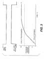
- FIG. 3is a timing diagram of the voltage threshold of a prior art single-bit per cell EANVM system being programmed from an erased “1” state to a programmed “0”.
- FIG. 4is a timing diagram of the bit line voltage of a prior single-bit per cell EANVM during a read operation. It illustrates waveform levels for both the programmed and erased conditions.
- FIG. 5is a block diagram of an M ⁇ N memory array implementing a multi-bit per cell EANVM system.
- FIG. 6is a block diagram for reading a multi-bit per cell EANVM system.
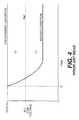
- FIG. 7shows the bit line voltage during a read cycle as a function of time for a 2-bit per cell EANVM which has been programmed to one of four possible states, (0, 0), (1, 0), (0, 1) and the fully erased condition (1, 1).
- Four separate voltage levelsare represented on this figure, each representing one of the four possible states. Only one of these would be present for any given read operation.
- FIG. 8is a block diagram of a multi-bit per cell system combining program/verify and read circuitry.
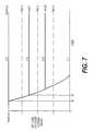
- FIG. 9is a timing diagrams for the voltage threshold for a 2-bit per cell EANVM being programmed from a fully erased (1, 1) state to one of the other three possible states.
- FIG. 10is a timing diagram which illustrates the voltage threshold of a 2-bit per cell EANVM being erased from a fully programmed (0,0) state to one of the other three possible states.
- FIG. 11is a timing diagram illustrating the voltage threshold of a 2-bit per cell EANVM during a program/verify cycle using fixed width program pulses.
- FIG. 12is a timing diagram illustrating the bit line voltage of a 2-bit per cell EANVM during a program/verify process which uses fixed width program pulses.
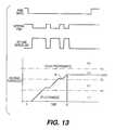
- FIG. 13is a timing diagram illustrating the voltage threshold of a 2-bit per cell EANVM during a program/verify cycle using variable width program pulses.
- FIG. 14is a timing diagram illustrating the bit line voltage of a 2-bit per cell EANVM during a program/verify process which uses variable width program pulses.
- the invention described hereallows n-bits of information to be stored on and read from an Electrically Alterable Non-Volatile Memory (EANVM).
- EANVMElectrically Alterable Non-Volatile Memory
- Thisis accomplished by electrically varying the conductivity of the channel of a floating gate FET to be within any one of K n conductivity ranges where “K” represents the base of the numbering system being employed (in a binary system, “K” equals 2).
- Krepresents the base of the numbering system being employed (in a binary system, “K” equals 2).
- the conductivity rangeis then sensed and encoded. This forms the basis of an n-bit EANVM memory cell.
- the floating gate FET conductivityis electrically modified by using external programming hardware and algorithms which supply signals and voltages to the EANVM memory device.
- FIG. 1is a generic schematic representation of a non-volatile floating gate memory cell 10 . It is not intended that this schematic drawing is in any way indicative of the device structure. It is used to illustrate the fact that this invention refers to an FET memory cell which uses an electrically isolated, or floating, gate 14 to store charged particles for the purpose of altering the voltage threshold and hence channel conductivity of the FET memory cell 10 .
- the FET memory cell 10includes a control gate 12 which is used either to select the memory cell for reading or is used to cause electrons to be injected onto the floating gate 14 during the programming process.
- Floating gate 14is an electrically isolated structure which can indefinitely store electrons. The presence or absence of electrons on floating gate 14 alters the voltage threshold of the memory cell 10 and as a result alters the conductivity of its channel region.
- a drain region 16 of the FETis coupled to a source region 18 by a channel region 19 . When the floating gate 14 is fully erased and the control gate 12 has been selected, the channel region 19 is in the fully “on”, or high conductivity, state. When the floating gate 14 is fully programmed the channel region 19 is in the fully “off”, or low conductivity state.
- FIG. 2is a block diagram of a prior art conventional single-bit EANVM memory system 30 .
- the memory system 30stores a single bit of information in an EANVM cell 32 .
- the cell 32as described in FIG. 1, is selected for reading or writing when a row, or word, select signal is applied to a control gate terminal 34 .
- a source terminal 36 for the FET of the cell 32is connected to a reference ground potential.
- a drain terminal 38is connected through a pull-up device 39 to a voltage Vpull-up at a terminal 40 . Terminal 38 serves as the output terminal of the cell 32 .
- the channel of the FETWhen the cell 32 stores a “0” bit, the channel of the FET is in a low conductivity, or high impedance, state so that the voltage at terminal 38 is pulled-up to the voltage level Vpull-up on terminal 40 .
- the channel of the FETWhen the cell 32 stores a “1” bit, the channel of the FET is in a high conductivity, or low impedance, state so that the voltage at terminal 38 is pulled-down by the ground potential at terminal 36 .
- a sense amplifier 42For reading the value of the single-bit stored in the cell 32 , a sense amplifier 42 compares the voltage at terminal 38 with a reference voltage Vref at terminal 43 . If a “0” is stored on the EANVM cell 32 , the cell will be in a low conductivity state and as a result the voltage at terminal 38 is above the reference voltage at terminal 43 . For a “0” stored in the cell 32 , the output terminal 44 of the sense amplifier 42 will be a low voltage which will be transmitted through an output buffer 46 to a terminal 48 and then coupled to the I/O terminal 50 as a logical “0”.
- the cellis in a high conductivity state and as a result the voltage at terminal 38 is below the reference voltage at terminal 43 .
- the output of the sense amplifier 42will be a high voltage which will be transmitted to the I/O terminal 50 as a logical “1”.
- the I/O terminal 50is connected to the input terminal of an input latch/buffer 52 .
- the output of the input latch/buffer 52is connected to an enable/disable terminal 54 of a program voltage switch 56 .
- the program voltage switch 56provides a bit-line program voltage on a signal line 58 connected to terminal 38 .
- Another output from the program voltage switch 56is the word line program voltage on a signal line 62 , which is connected to the control gate 34 of the EANVM cell 32 .
- the program voltage switch 56When a logical “0” is present at terminal 54 of the program voltage switch 56 from the output of Input Latch/Buffer 52 and when the program voltage switch 56 is activated by a program pulse on a signal line 62 from a program pulse 66 , activated by a PGM/Write signal, the program voltage switch 56 provides the Program Voltage Vpp from a terminal 68 to the control gate 34 of the EANVM cell 32 .
- the program voltage switch 56also biases the drain of the EANVM cell 32 to a voltage, typically between 8 to 9 volts, and the gate of the EANVM cell 32 to the program voltage Vpp, typically 12 volts. Under these conditions, electrons are injected onto the floating gate by a phenomenon known as hot electron injection.
- FIG. 3is a timing diagram of a prior-art single-bit EANVM cell 32 , as described in connection with FIG. 2 .
- the timing diagramshows the change in voltage threshold of the EANVM cell 32 , as controlled by the word line and bit line programming voltages, which are illustratively shown as a single signal and which are both controlled by the PGM/Write signal.
- the memory cellis being programmed from the fully erased “1” state to the fully programmed “0” state.
- the bit and word line program voltageswhich need not be the same, are respectively applied to the drain connected to the bit line terminal 38 and to the control gate 34 of the memory cell 32 .
- the voltage threshold of the memory cellbegins to increase. Once the voltage threshold has been increased beyond a specific threshold value as indicated by the dashed horizontal line, the memory cell 32 is programmed to a “0” state.
- the multi-bit EANVM device described herefunctions with either memory cell programming technique.
- the prior art programming algorithms and circuits for either type of programmingare designed to program a single-bit cell with as much margin as possible in as short a time as possible.
- marginis defined as the additional voltage threshold needed to insure that the programmed cell will retain its stored value over time.
- FIG. 4is a timing diagram showing the bit line voltage at terminal 38 as a function of time during a memory read operation.
- the bit lineis charged to the Vpull-up condition. Note that it is also possible that the bit line may start at any other voltage level prior to time t1.
- the EANVM cell 32is selected and, if the cell 32 is in the erased or “1” state, the cell 32 provides a low impedance path to ground. As a result, the bit line is pulled down to near the ground potential provided at terminal 36 in FIG. 2 . If the EANVM cell 32 were in the “0” or fully programmed state, the bit line voltage would remain at the Vpull-up voltage after time t1.
- the voltage on the bit-line terminal 38 and the reference voltage Vref at terminal 43are compared by the comparator 42 , whose buffered output drives I/O terminal 50 .
- Vrefis greater than the bit line voltage
- the output on I/O terminal 50is a logical “1”.
- the output on I/O terminal 50is a logical “0”.
- FIG. 5is a block diagram of a multi-bit per cell EANVM system 100 which includes an M ⁇ N array of memory cells.
- the cellsare typically shown as a floating gate FET, or EANVM, 102 , as described in connection with FIG. 1 .
- the arrayuses similar addressing techniques, external control signals, and I/O circuits as are used with currently available single bit per cell EANVM devices such as EPROM, EEPROM, FLASH, etc. devices.
- Row Address signalsare provided at input terminals 103 A and Column Address signals are provided at input terminals 103 B.
- Each of the EANVM cells in a row of cellshas its source connected to a ground reference potential and its drain connected to a column bit line, typically shown as 106 .
- Each of the columnsis connected to a pull-up device, as indicated by the block 105 .
- All of the control gates of a roware connected to a row select, or word, line, typically shown as 104 . Rows are selected with a row select circuit 108 and columns are selected with a column select circuit 110 .
- Sense amplifiers 112are provided for each of the selected columns.
- Decode/encode circuits 114 and n-bit input/output latches/buffers 116are also provided.
- a PGM/Write signalis provided at an input terminal 118 for activating a mode control circuit 120 and a timing circuit 122 .
- n-bit per cell system 100as compared to a single-bit per cell implementation is that the memory density is increased by a factor of n, where n is the number of bits which can be stored on an individual multi-bit memory cell.
- FIG. 6shows a binary system 150 for reading the state of an n-bit floating gate memory cell 102 , as described in connection with FIG. 1, according to the invention, where n is the number of bits stored in the memory cell.
- nis set to 2 and one of four states of the memory cell must be detected. The four possible states being, (0,0), (0,1), (1,0), or (1,1).
- Detecting which state is programmedrequires a 3-level sense amplifier 152 .
- This amplifierincludes three sense amplifiers 154 , 156 , 158 each of which have their negative input terminals connected to the output terminal 168 of the memory cell 102 .
- Sense amplifier 154has a reference voltage Ref 3 connected to its positive input terminal.
- Sense amplifier 156has a reference voltage Ref 2 connected to its positive input terminal.
- Sense amplifier 158has a reference voltage Ref 1 connected to its positive input terminal.
- the voltage referencesare set such as follows: Vpull-up>Ref 3>Ref 2>Ref 1.
- the respective output signals S 3 , S 2 , S 1 of the three sense amplifiersdrive an encode logic circuit 160 , which encodes the sensed signals S 3 , S 2 , S 1 into an appropriate 2-bit data format. Bit 0 is provided at an I/O terminal 162 and Bit 1 is provided at an I/O terminal 164 .
- a truth table for the encode logic circuit 160is as follows:
- the levels of the respective output signals S 3 , S 2 , S 1 of the sense amplifiers 154 , 156 , 158are determined by the conductivity value to which the memory cell had been set during a programming operation.
- a fully erased EANVM cell 102will be in its lowest threshold voltage state, or the highest conductivity state. Consequently, all of the reference voltages will be higher than the bit line voltage at terminal 168 , resulting in a (1,1) state.
- a fully programmed EANVM cell 102will be in its highest threshold voltage state, or its lowest conductivity state. Consequently, all reference voltages will be lower than the bit line voltage at terminal 168 , resulting in a (0,0) state.
- FIG. 7shows the bit line voltage as a function of time at terminal 106 , during a read cycle, for a binary 2-bit per memory cell. For purposes of illustration, each of the four possible waveforms corresponding to the four possible programmed states of the memory cell are shown. During a read cycle only the waveform corresponding to the programmed state of the EANVM cell would occur. For example, assume the EANVM memory cell 102 has been programmed to a (1,0) state. Prior to time t1, because the EANVM cell 102 has not yet been selected or activated, the bit line 106 is pulled-up to Vpull-up.
- the EANVM cellis selected using conventional memory address decoding techniques. Because the EANVM cell has been programmed to a specific conductivity level by the charge on the floating gate, the bit line is pulled down to a specific voltage level corresponding to the amount of current that the cell can sink at this specific conductivity level. When this point is reached at time t2 the bit line voltage stabilizes at a voltage level Vref3 between reference voltages Ref 3 and Ref 2 which correspond to a (1,0) state. When the EANVM cell 102 is de-selected, the bit line voltage will return to its pulled-up condition. Similarly, the bit-line voltage stabilizes at Vref2 the 0,1 state for, or at zero volts for the 1,1 state. FIG.
- FIG. 8is a block diagram of an n-bit memory cell system 200 .
- nis greater than 2.
- the inventioninclude any system where the EANVM memory cell has more than two states.
- the memory statescan be three or some other multiple of a non-binary system.
- Some of the components of this system 200are shown and described with the same reference numerals for the components of FIG. 6 for the read mode of operation. It is intended that these same reference numerals identify the same components.
- the system 200includes a memory cell 102 , as described in FIG. 1, with a bit line output terminal 168 .
- a 3-level sense amplifier 152 with read reference voltages Ref 1, Ref 2, and Ref 3 and an encoder 160is provided. Read data is provided at a Bit I/O terminal 162 and at a Bit 1 I/O terminal 164 .
- a verify reference voltage select circuit 222provides an analog voltage reference level signal X to one input terminal of an analog comparator 202 . The verify reference voltages are chosen so that as soon as the bit line voltage on bit line 106 is greater than the verify reference voltage the threshold of the EANVM cell 102 is set to the proper threshold corresponding to the memory state to which it is to be programmed.
- the verify reference voltages Vref1, Vref2, Vref3, and Vref4are set such that Vref4 is above Ref 3, Vref3 is between Ref 3 and Ref 2, Vref2 is between Ref 1 and Ref 2, and Vref1 is below Ref 1.
- the verify reference voltage select circuit 222is controlled by the 2-output bits from a 2-bit input latch/buffer circuit 224 , which receives binary input bits from the I/O terminals 162 and 164 .
- the Y signal input terminal of the analog comparator 202is connected to the bit line output terminal 168 of the multi-level memory cell 102 .
- the output signal from the analog comparatoris provided on a signal line 204 as an enable/disable signal for the program voltage switch 220 .
- An output signal line 206 from the program voltage switch 220provides the word line program voltage to the control gate of the EANVM cell 102 .
- Another output signal line 106provides the bit- line programming voltage to the bit- line terminal 168 of EANVM cell 102 .
- the timing circuit 208After a program/verify timing circuit 208 is enabled by a PGM/Write signal provided on a signal line 212 from a PGM/Write terminal 214 , the timing circuit 208 provides a series of program/verify timing pulses to the program voltage switch 220 on a signal line 210 .
- the pulse widthsare set to control the programming process so that the voltage threshold of the EANVM cell 102 is incrementally altered by controlling the injection of charge onto the floating gate of the EANVM cell.
- Each programming cycleincreases the voltage threshold and, as a result, decreases the conductance of the memory cell 102 .
- the program voltagesAfter each internal program cycle is complete, as indicated by signal line 210 going “high”, the program voltages are removed via the program voltage switch 220 and a verify cycle begins.
- the voltage threshold of memory cell 102is then determined by using the comparator 202 to compare the bit line voltage at terminal 168 with the selected verify reference voltage from the verify reference voltage select circuit 222 . When the bit line voltage exceeds that supplied by the verify reference voltage select circuit 222 , the output signal 204 from the comparator 202 will then disable the program voltage switch 220 ending the programming cycle.
- comparison of the current memory cell analog contents with the analog information to be programmed on the memory cell 102is performed by the analog comparator 202 .
- the Y input signal to the analog comparator 202is taken directly from the bit line terminal 168 .
- the 3-level sense/encode circuits 152 , 160 , and reference voltage select circuit 222may be completely independent, as indicated in the drawing. Alternatively, they may be coupled together to alternately time share common circuit components. This is possible because the 3-level sense/encode circuits 152 and 160 are used in the read mode of operation while the verify reference voltage select circuit 222 is used only in the write/verify mode of operation.
- a binary n-bit per cell EANVM systemIn the write mode, a binary n-bit per cell EANVM system must be capable of electrically programming a memory cell to 2 n uniquely different threshold levels.
- Vt 1 , Vt 2 , and Vt 3which define the (0,1), (1,0), and (0,0) states.
- Vt 1is the threshold required such that in the read mode, the bit line voltage will fall between Ref 1 and Ref 2.
- Vt 2is the threshold required such that in the read mode, the bit line voltage will fall between Ref 2 and Ref 3.
- Vt 3is the threshold required such that in the read mode, the bit line voltage will be greater than Ref 3.
- FIG. 9illustrates the change in voltage threshold for a 4-level, or 2-bit EANVM cell as the floating gate is being charged from an erased (1,1) threshold state to any one of the three other possible states.
- the design objectiveis to provide enough charge to the floating gate to insure that the cell's voltage threshold is programmed as high as possible, as shown in FIG. 3 . Because there is no upper threshold limit in a single-bit per cell system, overprogramming the cell will not cause incorrect data to be stored on the memory cell.
- the memory cellin an n-bit per cell system the memory cell must be charged to a point so that the voltage threshold is within a specific voltage threshold range.
- the proper threshold rangeis defined as being above a threshold level Vt 2 and as being below a threshold level Vt 3 .
- FIG. 8shows the additional or modified circuits, including a reference voltage select, an n-bit latch/buffer, a program/verify timing circuit, and a comparator.
- the comparatorcan be either digital or analog.
- FIG. 10illustrates the voltage threshold of an EANVM cell as the floating gate is being erased from a (0,0) state.
- Standard EANVM programming operating procedurecalls for a memory cell to be erased prior to being programmed. This erasure can be performed at the byte, block, or chip level and can be performed by electrical, UV, or other means. In this type of system the cell would be completely erased to a (1,1) state prior to initiating a programming cycle. If a system has the capability to erase an individual memory cell, then it is not necessary to erase all of the cells of a group prior to initiating a programming operation. It is then possible to incrementally erase an individual memory cell, as necessary, to program the cell to the appropriate voltage threshold as is indicated by the waveforms labelled (1,0) and (0,1).
- FIG. 11is a timing diagram which illustrates how a 2-bit EANVM cell of FIG. 8 is programmed from an erased (1,1) state to a (1,0) state using the timing circuitry 208 to generate fixed length timing pulses.
- a low logic level state of the PGM/Write signal on signal line 212enables the timing circuit 208 .
- the timing circuit 208When enabled at time t1, the timing circuit 208 provides an internal fixed-width low level internal PGM timing pulse on signal line 210 to the program voltage switch 220 .
- the bit line and word line program voltage outputs on lines 106 and 206will be raised to their respective programming voltage levels as shown in FIG. 11 .
- FIG. 12illustrates the bit line voltage of a 2-bit per cell EANVM as it is being programmed from a fully erased, or fully “on”, state (1,1) to a partially “off” state (1, 0) using fixed length program pulses.
- the program/verify timing circuit 208first initiates a verify cycle to determine the current status of the memory cell 102 . This is indicated by the bit line voltage being pulled to a ground condition from, in this example, Vpull-up. More generally, prior to time t1, the bit line voltage could be pre-set to any voltage level.
- the first program cycleis initiated. This is represented by the bit line voltage being pulled up to Vprogram.
- a verify cyclebegins. This is represented by the bit line voltage being pulled down to a point midway between ground potential and Ref1. During each successive verify cycle the bit line voltage is observed to incrementally increase. This program/verify cycle continues until the bit-line voltage exceeds the selected verify reference voltage, in this case Vref3, which indicates a memory state of (1,0), at time t2.
- FIG. 13illustrates how a 2-bit EANVM cell is programmed from an erased (1,1) state to a (1,0) state using variable length programming pulses.
- the internal PGM pulses for this implementationstart with a low state longer than for fixed-width implementation of FIGS. 11 and 12.
- the low-state pulse widthsgrow progressively shorter as the memory cell approaches the appropriate voltage threshold. This approach requires more precise control than the fixed length approach. However, programming times can be greatly reduced on average.
- FIG. 14illustrates the bit line voltage of a 2-bit per cell EANVM as it is being programmed from a fully erased, or fully “on”, state (1,1) to a partially “off” state (1,0) using variable length program pulses.
- the program/verify timing circuit 208first initiates a verify cycle to determine the current status of the memory cell 102 . This is indicated by the bit line voltage being pulled to a ground condition from, in this example, Vpull-up. Although, prior to time t1, the bit line voltage could be pre-set to any voltage level.
- the first program cycleis initiated. This is represented by the bit line voltage being pulled up to Vprogram. After the first variable length programming pulse is over, another verify cycle begins. This is represented by the bit line voltage being pulled down to a point midway between Ref1 and Ref2. During each successive verify cycle the bit line voltage is observed to incrementally increase. This program/verify cycle continues until the bit-line voltage surpasses the selected verify reference voltage, in-this case Vref3 which indicates a memory state of (1,0), at time t2.
- the programming process for an n-bit per cell EANVMuses program/verify cycles, to incrementally program a cell.
- the durations of these cyclesare determined by the timing circuit 208 .
- a key element of the systemis to provide a programming scheme which provides for accurate programming of the memory cell 102 . This is accomplished by matching the pulse widths of the timing pulses of the timing circuitry 208 to the program time of the EANVM cell being used. As indicated in FIGS. 11 and 13, a desired voltage threshold actually falls within a range of threshold voltages. If the program pulses are too long, then too much charge may be added to the floating gate of the memory cell 102 . This may result in an overshoot of the target voltage threshold, resulting in incorrect data being stored in the memory cell.
- the programming pulse widthis set such that if the voltage threshold of the cell 102 after the (n-1) programming pulse is at a point just below the target voltage threshold, then the (n)th, or final, program pulse will not cause an overshoot resulting in an overprogrammed condition for a memory cell.
- FIG. 8may also use a digital comparator rather than the analog comparator 202 shown in FIG. 8 .
- the digital comparatorwould use the encoded data from the encode circuitry 160 , which represents the current contents of the EANVM cell 102 , as the input to the comparator represent the.
- the verify reference voltage select 222would provide the voltage to be encoded with the input coming from the output of the n-bit input latch/buffer 224 , representing the data to be programmed. Otherwise, the function of the comparator within the system remains the same.
Landscapes
- Engineering & Computer Science (AREA)
- Computer Hardware Design (AREA)
- Read Only Memory (AREA)
Abstract
Description
This application is a division of Ser. No. 09/195,201, filed Nov. 18, 1998, which is a division of Ser. No. 08/911,731 filed Aug. 15, 1997, now U.S. Pat. No. 5,872,235 which is a division of Ser. No. 08/410,200 filed Feb. 27, 1995, now U.S. Pat. No. 5,764,571 which is a division of U.S. patent application Ser. No. 08/071,816, filed Jun. 4, 1993, now U.S. Pat. No. 5,394,362 entitled “Electrically Alterable Non-Volatile Memory with N-Bits Per Memory Cell,” which is a continuation of U.S. patent application Ser. No. 07/652,878, filed Feb. 8, 1991 (now U.S. Pat. No. 5,218,569) entitled “Electrically Alterable Non-Volatile Memory with N-Bits Per Cell.”
1. Field of the Invention
This invention relates to non-volatile memory (NVM) devices; and, more particularly, is concerned with an apparatus and method for programming and/or verifying programming of a multi-level NVM device.
2. Description of the Background Art
In conventional single-bit per cell memory devices, the memory cell assumes one of two information storage states, either an “on” state or an “off” state. This combination of either “on” or “off” defines one bit of information. As a result, a memory device which can store n-bits of data requires n separate memory cells.
Increasing the number of bits which can be stored in a single-bit per cell memory device relies upon increasing the number of memory cells on a one-for-one basis with the number of bits of data to be stored. Methods for increasing the number of memory bits in a single memory device have relied upon the following advanced manufacturing techniques: manufacture larger die which contain more memory cells; or use improved lithography techniques to build smaller memory cells and allow more memory cells to be placed in a given area on a single chip.
An alternative approach to the single-bit per cell approach involves storing multiple-bits of data in a single memory cell. Previous approaches to implementing multiple-bit per cell non-volatile memory devices have only involved mask programmable read only memories (ROMs). In one of these approaches, the channel width and/or length of the memory cell is varied such that 2ndifferent conductivity values are obtained which correspond to 2ndifferent states corresponding to n-bits of data which can be stored on a single memory cell. In another approach, the ion implant for the threshold voltage is varied such that the memory cell will have 2ndifferent voltage thresholds (Vt) corresponding to 2ndifferent conductance levels corresponding to 2ndifferent states corresponding to n-bits of data which can be stored on a single memory cell. Examples of memory devices of these types are described in U.S. Pat. No. 4,192,014 by Craycraft, U.S. Pat. No. 4,586,163 by Koike, U.S. Pat. No. 4,287,570 by Stark, U.S. Pat. No. 4,327,424 by Wu, and U.S. Pat. No. 4,847,808 by Kobatake.
Single-bit per cell read-only-memory devices are only required to sense, or read, two different levels or states per cell, consequently they have need for only one voltage reference. Sensing schemes for multi-level memory devices are more complex and require 21−1 voltage references. Examples of such multiple state sensing schemes for ROMs are described in U.S. Pat. No. 4,449,203 by Adlhoch, U.S. Pat. No. 4,495,602 by Shepard, U.S. Pat. No. 4,503,578 by Iwahashi, and U.S. Pat. No. 4,653,023 by Suzuki.
These approaches to a multi-bit ROM commonly have one of 2ndifferent conductivity levels of each memory cell being determined during the manufacturing process by means of a customized mask that is valid for only one data pattern. Thus, for storing n different data information patterns, a minimum of n different masks need to be produced and incorporated into a manufacturing process. Each time a data information pattern needs to be changed a new mask must be created and a new batch of semiconductor wafers processed. This dramatically increases the time between a data pattern change and the availability of a memory product programmed with that new data pattern.
Prior art electrically alterable multiple-bit per cell memory approaches store multiple levels of charge on a capacitive storage element, such as is found in a conventional dynamic random access memory (DRAM) or a charge coupled device (CCD). Such approaches are described in U.S. Pat. No. 4,139,910 by Anantha, U.S. Pat. No. 4,306,300 by Terman, U.S. Pat. No. 4,661,929 by Aoki, U.S. Pat. No. 4,709,350 by Nakagome, and U.S. Pat. No. 4,771,404 by Mano. All of these approaches use volatile storage, that is, the charge levels are not permanently stored. They provide 2ndifferent volatile charge levels on a capacitor to define 2ndifferent states corresponding to n-bits of data per memory cell. All of these approaches have the common characteristic that whatever information is stored on such a memory cell is volatile because such a cell loses its data whenever power is removed. Furthermore, these types of memory cells must be periodically refreshed as they have a tendency to lose charge over time even when power is maintained.
It would be advantageous to develop a multi-bit semiconductor memory cell that has the non-volatile characteristic of a mask programmable read-only-memory (ROM) and the electrically alterable characteristic of a multi-bit per cell DRAM. These characteristics combined in a single cell would provide a multi-bit per cell electrically alterable non-volatile memory (EANVM) capable of storing Knbits of data, where “K” is the base of the numbering system being used and “n” is the number of bits to be stored in each memory cell. Additionally, it would be advantageous if the EANVM described above was fully compatible with conventional industry standard device programmers/erasers and programming/erasing algorithms such that a user can program/erase the multi-bit per cell memory in a manner identical to that used for current single-bit per cell memory devices.
The present invention provides a multi-level electrically alterable non-volatile memory (EANVM) device, wherein some or all of the storage locations have more than two distinct states.
In a specific embodiment, the present invention provides a multi-level memory device. The present multi-level memory device includes a multi-level cell means for storing input information for an indefinite period of time as a discrete state of the multi-level cell means. The multi-level cell means stores information in Knmemory states, where K is a base of a predetermined number system, n is a number of bits stored per cell, and Kn>2. The present multi-level memory device also includes a memory cell programming means for programming the multi-level cell means to a state corresponding to the input information. A comparator means for comparing the memory state of the multi-level cell means with the input information is also included. The input information corresponds to one of a plurality of reference voltages. The present comparator means further generates a control signal indicative of the memory state as compared to the input information.
An alternative specific embodiment also provides a multi-level memory device. The present multi-level memory device includes a multi-level cell means for storing input information for an indefinite period of time as a discrete state of the multi-level cell means. The multi-level cell means stores information in Knmemory states, where K is a base of a predetermined number system, n is a number of bits stored per cell, and Kn>2. A memory cell programming means for programming the multi-level cell means to a state corresponding to the input information is also included. The present multi-level memory device further includes a comparator means for comparing the memory state of the multi-level cell means with the input information. The input information corresponds to one of a plurality of reference voltages. The present comparator means further generates a control signal indicative of the memory state as compared to the input information. A reference voltage means for defining the plurality of reference voltages is also included. The present reference voltage means is operably coupled to the comparator means.
The accompanying drawings, which are incorporated in and form a part of this specification, illustrate embodiments of the invention and, together with the description, serve to explain the principles of the invention:
FIG. 1 is a generic schematic representation of a non-volatile floating gate memory cell.
FIG. 2 is a block diagram of a prior art single-bit memory system.
FIG. 3 is a timing diagram of the voltage threshold of a prior art single-bit per cell EANVM system being programmed from an erased “1” state to a programmed “0”.
FIG. 4 is a timing diagram of the bit line voltage of a prior single-bit per cell EANVM during a read operation. It illustrates waveform levels for both the programmed and erased conditions.
FIG. 5 is a block diagram of an M×N memory array implementing a multi-bit per cell EANVM system.
FIG. 6 is a block diagram for reading a multi-bit per cell EANVM system.
FIG. 7 shows the bit line voltage during a read cycle as a function of time for a 2-bit per cell EANVM which has been programmed to one of four possible states, (0, 0), (1, 0), (0, 1) and the fully erased condition (1, 1). Four separate voltage levels are represented on this figure, each representing one of the four possible states. Only one of these would be present for any given read operation.
FIG. 8 is a block diagram of a multi-bit per cell system combining program/verify and read circuitry.
FIG. 9 is a timing diagrams for the voltage threshold for a 2-bit per cell EANVM being programmed from a fully erased (1, 1) state to one of the other three possible states.
FIG. 10 is a timing diagram which illustrates the voltage threshold of a 2-bit per cell EANVM being erased from a fully programmed (0,0) state to one of the other three possible states.
FIG. 11 is a timing diagram illustrating the voltage threshold of a 2-bit per cell EANVM during a program/verify cycle using fixed width program pulses.
FIG. 12 is a timing diagram illustrating the bit line voltage of a 2-bit per cell EANVM during a program/verify process which uses fixed width program pulses.
FIG. 13 is a timing diagram illustrating the voltage threshold of a 2-bit per cell EANVM during a program/verify cycle using variable width program pulses.
FIG. 14 is a timing diagram illustrating the bit line voltage of a 2-bit per cell EANVM during a program/verify process which uses variable width program pulses.
Reference will now be made in detail to the specific embodiments of the invention, examples of which are illustrated in the accompanying drawings. While the invention will be described in conjunction with the specific embodiments, it will be understood that they are not intended to limit the invention to those embodiments. On the contrary, the invention is intended to cover various alternatives, modifications and equivalents, which may be included within the spirit and scope of the invention as defined by the appended claims.
In general, the invention described here allows n-bits of information to be stored on and read from an Electrically Alterable Non-Volatile Memory (EANVM). This is accomplished by electrically varying the conductivity of the channel of a floating gate FET to be within any one of Knconductivity ranges where “K” represents the base of the numbering system being employed (in a binary system, “K” equals 2). The conductivity range is then sensed and encoded. This forms the basis of an n-bit EANVM memory cell. The floating gate FET conductivity is electrically modified by using external programming hardware and algorithms which supply signals and voltages to the EANVM memory device.
These external signals and voltages are then modified internal to the device to provide an internally controlled program/verify cycle which incrementally stores electrons on the floating gate until the desired conductivity range is achieved. For the purpose of illustration, the n-bit per cell descriptions will assume a binary system which stores 2-bits per memory cell.
FIG. 1 is a generic schematic representation of a non-volatile floatinggate memory cell 10. It is not intended that this schematic drawing is in any way indicative of the device structure. It is used to illustrate the fact that this invention refers to an FET memory cell which uses an electrically isolated, or floating,gate 14 to store charged particles for the purpose of altering the voltage threshold and hence channel conductivity of theFET memory cell 10.
TheFET memory cell 10 includes acontrol gate 12 which is used either to select the memory cell for reading or is used to cause electrons to be injected onto the floatinggate 14 during the programming process. Floatinggate 14 is an electrically isolated structure which can indefinitely store electrons. The presence or absence of electrons on floatinggate 14 alters the voltage threshold of thememory cell 10 and as a result alters the conductivity of its channel region. Adrain region 16 of the FET is coupled to asource region 18 by achannel region 19. When the floatinggate 14 is fully erased and thecontrol gate 12 has been selected, thechannel region 19 is in the fully “on”, or high conductivity, state. When the floatinggate 14 is fully programmed thechannel region 19 is in the fully “off”, or low conductivity state.
FIG. 2 is a block diagram of a prior art conventional single-bitEANVM memory system 30. Thememory system 30 stores a single bit of information in anEANVM cell 32. Thecell 32, as described in FIG. 1, is selected for reading or writing when a row, or word, select signal is applied to acontrol gate terminal 34. Asource terminal 36 for the FET of thecell 32 is connected to a reference ground potential. Adrain terminal 38 is connected through a pull-updevice 39 to a voltage Vpull-up at a terminal40.Terminal 38 serves as the output terminal of thecell 32. When thecell 32 stores a “0” bit, the channel of the FET is in a low conductivity, or high impedance, state so that the voltage atterminal 38 is pulled-up to the voltage level Vpull-up onterminal 40. When thecell 32 stores a “1” bit, the channel of the FET is in a high conductivity, or low impedance, state so that the voltage atterminal 38 is pulled-down by the ground potential atterminal 36.
For reading the value of the single-bit stored in thecell 32, asense amplifier 42 compares the voltage at terminal38 with a reference voltage Vref atterminal 43. If a “0” is stored on theEANVM cell 32, the cell will be in a low conductivity state and as a result the voltage atterminal 38 is above the reference voltage atterminal 43. For a “0” stored in thecell 32, theoutput terminal 44 of thesense amplifier 42 will be a low voltage which will be transmitted through anoutput buffer 46 to a terminal48 and then coupled to the I/O terminal 50 as a logical “0”. If a “1” is stored on theEANVM cell 32, the cell is in a high conductivity state and as a result the voltage atterminal 38 is below the reference voltage atterminal 43. The output of thesense amplifier 42 will be a high voltage which will be transmitted to the I/O terminal 50 as a logical “1”.
For writing the value of an information bit stored in thecell 32, it is assumed that thecell 32 is in the erased, or fully “on”, state which corresponds to a logical “1”. The I/O terminal 50 is connected to the input terminal of an input latch/buffer 52. The output of the input latch/buffer 52 is connected to an enable/disableterminal 54 of aprogram voltage switch 56. Theprogram voltage switch 56 provides a bit-line program voltage on asignal line 58 connected toterminal 38. Another output from theprogram voltage switch 56 is the word line program voltage on asignal line 62, which is connected to thecontrol gate 34 of theEANVM cell 32. When a logical “0” is present atterminal 54 of the program voltage switch56 from the output of Input Latch/Buffer 52 and when theprogram voltage switch 56 is activated by a program pulse on asignal line 62 from aprogram pulse 66, activated by a PGM/Write signal, theprogram voltage switch 56 provides the Program Voltage Vpp from a terminal68 to thecontrol gate 34 of theEANVM cell 32. Theprogram voltage switch 56 also biases the drain of theEANVM cell 32 to a voltage, typically between 8 to 9 volts, and the gate of theEANVM cell 32 to the program voltage Vpp, typically 12 volts. Under these conditions, electrons are injected onto the floating gate by a phenomenon known as hot electron injection. This programming procedure raises the voltage threshold of the EANVM cell which increases its source-drain impedance. This continues until theFET memory cell 32 is effectively turned off, which corresponds to a “0” state. When a “1” is present on terminal54 from the output of the Input Latch/Buffer 52 and when the PGM/Write is enabled, thesignal line 58 is driven low and programming is inhibited and the “1”, or erased, state is maintained.
FIG. 3 is a timing diagram of a prior-art single-bit EANVM cell 32, as described in connection with FIG.2. The timing diagram shows the change in voltage threshold of theEANVM cell 32, as controlled by the word line and bit line programming voltages, which are illustratively shown as a single signal and which are both controlled by the PGM/Write signal. The memory cell is being programmed from the fully erased “1” state to the fully programmed “0” state. For the duration of the PGM/Write pulse, the bit and word line program voltages, which need not be the same, are respectively applied to the drain connected to thebit line terminal 38 and to thecontrol gate 34 of thememory cell 32. As electrons are injected onto the floating gate, the voltage threshold of the memory cell begins to increase. Once the voltage threshold has been increased beyond a specific threshold value as indicated by the dashed horizontal line, thememory cell 32 is programmed to a “0” state.
Note that Fowler-Nordheim tunnelling can also be used instead of hot electron injection to place electrons on the floating gate. The multi-bit EANVM device described here functions with either memory cell programming technique. The prior art programming algorithms and circuits for either type of programming are designed to program a single-bit cell with as much margin as possible in as short a time as possible. For a single-bit memory cell, margin is defined as the additional voltage threshold needed to insure that the programmed cell will retain its stored value over time.
FIG. 4 is a timing diagram showing the bit line voltage atterminal 38 as a function of time during a memory read operation. In this example, prior to time t1 the bit line is charged to the Vpull-up condition. Note that it is also possible that the bit line may start at any other voltage level prior to time t1. At time t1, theEANVM cell 32 is selected and, if thecell 32 is in the erased or “1” state, thecell 32 provides a low impedance path to ground. As a result, the bit line is pulled down to near the ground potential provided atterminal 36 in FIG.2. If theEANVM cell 32 were in the “0” or fully programmed state, the bit line voltage would remain at the Vpull-up voltage after time t1. The voltage on the bit-line terminal 38 and the reference voltage Vref atterminal 43 are compared by thecomparator 42, whose buffered output drives I/O terminal 50. When Vref is greater than the bit line voltage, the output on I/O terminal 50 is a logical “1”. When Vref is lower than the bit line voltage, the output on I/O terminal 50 is a logical “0”.
FIG. 5 is a block diagram of a multi-bit percell EANVM system 100 which includes an M×N array of memory cells. The cells are typically shown as a floating gate FET, or EANVM,102, as described in connection with FIG.1. The array uses similar addressing techniques, external control signals, and I/O circuits as are used with currently available single bit per cell EANVM devices such as EPROM, EEPROM, FLASH, etc. devices. Row Address signals are provided atinput terminals 103A and Column Address signals are provided atinput terminals 103B.
Each of the EANVM cells in a row of cells has its source connected to a ground reference potential and its drain connected to a column bit line, typically shown as106. Each of the columns is connected to a pull-up device, as indicated by theblock 105. All of the control gates of a row are connected to a row select, or word, line, typically shown as104. Rows are selected with a rowselect circuit 108 and columns are selected with a columnselect circuit 110.Sense amplifiers 112 are provided for each of the selected columns. Decode/encodecircuits 114 and n-bit input/output latches/buffers 116 are also provided. A PGM/Write signal is provided at aninput terminal 118 for activating amode control circuit 120 and atiming circuit 122.
A significant feature of this n-bit percell system 100 as compared to a single-bit per cell implementation is that the memory density is increased by a factor of n, where n is the number of bits which can be stored on an individual multi-bit memory cell.
FIG. 6 shows abinary system 150 for reading the state of an n-bit floatinggate memory cell 102, as described in connection with FIG. 1, according to the invention, where n is the number of bits stored in the memory cell. For this example, n is set to 2 and one of four states of the memory cell must be detected. The four possible states being, (0,0), (0,1), (1,0), or (1,1). Detecting which state is programmed requires a 3-level sense amplifier 152. This amplifier includes threesense amplifiers output terminal 168 of thememory cell 102.Sense amplifier 154 has areference voltage Ref 3 connected to its positive input terminal.Sense amplifier 156 has areference voltage Ref 2 connected to its positive input terminal.Sense amplifier 158 has areference voltage Ref 1 connected to its positive input terminal. The voltage references are set such as follows: Vpull-up>Ref 3>Ref 2>Ref 1. The respective output signals S3, S2, S1 of the three sense amplifiers drive an encodelogic circuit 160, which encodes the sensed signals S3, S2, S1 into an appropriate 2-bit data format.Bit 0 is provided at an I/O terminal 162 andBit 1 is provided at an I/O terminal 164. A truth table for the encodelogic circuit 160 is as follows:
| S3 | S2 | S1 | I/O 1 | I/ | State | ||
| L | L | 0 | 0 | (0,0) | |||
| L | L | 1 | 0 | (1,0) | |||
| H | L | 0 | 1 | (0,1) | |||
| H | H | 1 | 1 | (1,1) | |||
During a read operation of an n-bit memory cell, the levels of the respective output signals S3, S2, S1 of thesense amplifiers EANVM cell 102 will be in its lowest threshold voltage state, or the highest conductivity state. Consequently, all of the reference voltages will be higher than the bit line voltage atterminal 168, resulting in a (1,1) state. A fully programmedEANVM cell 102 will be in its highest threshold voltage state, or its lowest conductivity state. Consequently, all reference voltages will be lower than the bit line voltage atterminal 168, resulting in a (0,0) state. The intermediate threshold states are encoded as is illustrated in the truth table for thelogic circuit 160. FIG. 7 shows the bit line voltage as a function of time atterminal 106, during a read cycle, for a binary 2-bit per memory cell. For purposes of illustration, each of the four possible waveforms corresponding to the four possible programmed states of the memory cell are shown. During a read cycle only the waveform corresponding to the programmed state of the EANVM cell would occur. For example, assume theEANVM memory cell 102 has been programmed to a (1,0) state. Prior to time t1, because theEANVM cell 102 has not yet been selected or activated, thebit line 106 is pulled-up to Vpull-up. At time t1, the EANVM cell is selected using conventional memory address decoding techniques. Because the EANVM cell has been programmed to a specific conductivity level by the charge on the floating gate, the bit line is pulled down to a specific voltage level corresponding to the amount of current that the cell can sink at this specific conductivity level. When this point is reached at time t2 the bit line voltage stabilizes at a voltage level Vref3 betweenreference voltages Ref 3 andRef 2 which correspond to a (1,0) state. When theEANVM cell 102 is de-selected, the bit line voltage will return to its pulled-up condition. Similarly, the bit-line voltage stabilizes at Vref2 the 0,1 state for, or at zero volts for the 1,1 state. FIG. 8 is a block diagram of an n-bitmemory cell system 200. For purposes of illustration a binary 2-bit per cell system is shown. However, the concepts of the invention extend to systems where n is greater than 2. It is also intended that the invention include any system where the EANVM memory cell has more than two states. For example, in a non-binary system, the memory states can be three or some other multiple of a non-binary system. Some of the components of thissystem 200 are shown and described with the same reference numerals for the components of FIG. 6 for the read mode of operation. It is intended that these same reference numerals identify the same components. Thesystem 200 includes amemory cell 102, as described in FIG. 1, with a bitline output terminal 168. For the read mode of operation, a 3-level sense amplifier 152 with readreference voltages Ref 1,Ref 2, andRef 3 and anencoder 160 is provided. Read data is provided at a Bit I/O terminal 162 and at a Bit1 I/O terminal 164. For the write mode of operation, a verify reference voltageselect circuit 222 provides an analog voltage reference level signal X to one input terminal of ananalog comparator 202. The verify reference voltages are chosen so that as soon as the bit line voltage onbit line 106 is greater than the verify reference voltage the threshold of theEANVM cell 102 is set to the proper threshold corresponding to the memory state to which it is to be programmed. To this end the verify reference voltages Vref1, Vref2, Vref3, and Vref4 are set such that Vref4 is aboveRef 3, Vref3 is betweenRef 3 andRef 2, Vref2 is betweenRef 1 andRef 2, and Vref1 is belowRef 1. During a normal read operation, the bit line voltage will settle midway between the read reference voltages to insure that the memory contents will be read accurately. The verify reference voltageselect circuit 222 is controlled by the 2-output bits from a 2-bit input latch/buffer circuit 224, which receives binary input bits from the I/O terminals analog comparator 202 is connected to the bitline output terminal 168 of themulti-level memory cell 102. The output signal from the analog comparator is provided on asignal line 204 as an enable/disable signal for theprogram voltage switch 220. Anoutput signal line 206 from theprogram voltage switch 220 provides the word line program voltage to the control gate of theEANVM cell 102. Anotheroutput signal line 106 provides the bit- line programming voltage to the bit-line terminal 168 ofEANVM cell 102. After a program/verifytiming circuit 208 is enabled by a PGM/Write signal provided on asignal line 212 from a PGM/Write terminal 214, thetiming circuit 208 provides a series of program/verify timing pulses to theprogram voltage switch 220 on asignal line 210. The pulse widths are set to control the programming process so that the voltage threshold of theEANVM cell 102 is incrementally altered by controlling the injection of charge onto the floating gate of the EANVM cell. Each programming cycle increases the voltage threshold and, as a result, decreases the conductance of thememory cell 102. After each internal program cycle is complete, as indicated bysignal line 210 going “high”, the program voltages are removed via theprogram voltage switch 220 and a verify cycle begins. The voltage threshold ofmemory cell 102 is then determined by using thecomparator 202 to compare the bit line voltage atterminal 168 with the selected verify reference voltage from the verify reference voltageselect circuit 222. When the bit line voltage exceeds that supplied by the verify reference voltageselect circuit 222, theoutput signal 204 from thecomparator 202 will then disable theprogram voltage switch 220 ending the programming cycle. For this embodiment of the invention, during a write operation, comparison of the current memory cell analog contents with the analog information to be programmed on thememory cell 102 is performed by theanalog comparator 202. The verify reference voltageselect circuit 222 analog output voltage X is determined by decoding the output of the n-bit input latch/buffer224 (n=2 in the illustrative form). The Y input signal to theanalog comparator 202 is taken directly from thebit line terminal 168. Note that the 3-level sense/encodecircuits select circuit 222 may be completely independent, as indicated in the drawing. Alternatively, they may be coupled together to alternately time share common circuit components. This is possible because the 3-level sense/encodecircuits select circuit 222 is used only in the write/verify mode of operation.
In the write mode, a binary n-bit per cell EANVM system must be capable of electrically programming a memory cell to 2nuniquely different threshold levels. In the two-bit per cell implementation, because it is assumed that the cell starts from the erased (1,1) state, it is only necessary to program three different thresholds (Vt1, Vt2, and Vt3) which define the (0,1), (1,0), and (0,0) states. Vt1 is the threshold required such that in the read mode, the bit line voltage will fall betweenRef 1 andRef 2. Vt2 is the threshold required such that in the read mode, the bit line voltage will fall betweenRef 2 andRef 3. Vt3 is the threshold required such that in the read mode, the bit line voltage will be greater thanRef 3.
FIG. 9 illustrates the change in voltage threshold for a 4-level, or 2-bit EANVM cell as the floating gate is being charged from an erased (1,1) threshold state to any one of the three other possible states. In prior art single-bit memory cells where there are only two states, the design objective is to provide enough charge to the floating gate to insure that the cell's voltage threshold is programmed as high as possible, as shown in FIG.3. Because there is no upper threshold limit in a single-bit per cell system, overprogramming the cell will not cause incorrect data to be stored on the memory cell.
As will be appreciated from FIG. 9, in an n-bit per cell system the memory cell must be charged to a point so that the voltage threshold is within a specific voltage threshold range. In this example, where the cell is being programmed to a (1,0) state, the proper threshold range is defined as being above a threshold level Vt2 and as being below a threshold level Vt3.
To accomplish this n-level programming it is necessary to add to or modify the prior art EANVM circuitry. FIG. 8 shows the additional or modified circuits, including a reference voltage select, an n-bit latch/buffer, a program/verify timing circuit, and a comparator. The comparator can be either digital or analog.
FIG. 10 illustrates the voltage threshold of an EANVM cell as the floating gate is being erased from a (0,0) state. Standard EANVM programming operating procedure calls for a memory cell to be erased prior to being programmed. This erasure can be performed at the byte, block, or chip level and can be performed by electrical, UV, or other means. In this type of system the cell would be completely erased to a (1,1) state prior to initiating a programming cycle. If a system has the capability to erase an individual memory cell, then it is not necessary to erase all of the cells of a group prior to initiating a programming operation. It is then possible to incrementally erase an individual memory cell, as necessary, to program the cell to the appropriate voltage threshold as is indicated by the waveforms labelled (1,0) and (0,1).
FIG. 11 is a timing diagram which illustrates how a 2-bit EANVM cell of FIG. 8 is programmed from an erased (1,1) state to a (1,0) state using thetiming circuitry 208 to generate fixed length timing pulses. A low logic level state of the PGM/Write signal onsignal line 212 enables thetiming circuit 208. When enabled at time t1, thetiming circuit 208 provides an internal fixed-width low level internal PGM timing pulse onsignal line 210 to theprogram voltage switch 220. For the duration of the low state of the internal PGM timing pulse, the bit line and word line program voltage outputs onlines memory cell 102. When the internal PGM timing pulse from timingcircuitry 208 switches to a high level, the programming voltages are removed and a verify cycle begins. For this example, verify reference voltage Vref3 is compared with the bit line voltage. This internally controlled program/verify cycle repeats itself until the bit line voltage onterminal 168 exceeds Vref3. At this time, t2, theEANVM cell 102 is verified to have been programmed to a (1,0) state and programming is halted by thecomparator 202 providing a disable signal onsignal line 204 to theprogram voltage switch 220.
FIG. 12 illustrates the bit line voltage of a 2-bit per cell EANVM as it is being programmed from a fully erased, or fully “on”, state (1,1) to a partially “off” state (1, 0) using fixed length program pulses. When the externally applied PGM/Write pulse is applied at time t1, the program/verifytiming circuit 208 first initiates a verify cycle to determine the current status of thememory cell 102. This is indicated by the bit line voltage being pulled to a ground condition from, in this example, Vpull-up. More generally, prior to time t1, the bit line voltage could be pre-set to any voltage level. Once the cell has been determined to be at a condition below the verify reference voltage, Vref3 in this example, corresponding to the data to be programmed, the first program cycle is initiated. This is represented by the bit line voltage being pulled up to Vprogram. After the first fixed length programming pulse ends, a verify cycle begins. This is represented by the bit line voltage being pulled down to a point midway between ground potential and Ref1. During each successive verify cycle the bit line voltage is observed to incrementally increase. This program/verify cycle continues until the bit-line voltage exceeds the selected verify reference voltage, in this case Vref3, which indicates a memory state of (1,0), at time t2.
FIG. 13 illustrates how a 2-bit EANVM cell is programmed from an erased (1,1) state to a (1,0) state using variable length programming pulses. The internal PGM pulses for this implementation start with a low state longer than for fixed-width implementation of FIGS. 11 and 12. The low-state pulse widths grow progressively shorter as the memory cell approaches the appropriate voltage threshold. This approach requires more precise control than the fixed length approach. However, programming times can be greatly reduced on average.
FIG. 14 illustrates the bit line voltage of a 2-bit per cell EANVM as it is being programmed from a fully erased, or fully “on”, state (1,1) to a partially “off” state (1,0) using variable length program pulses. When the externally applied PGM/Write pulse goes to an active low level at time t1, the program/verifytiming circuit 208 first initiates a verify cycle to determine the current status of thememory cell 102. This is indicated by the bit line voltage being pulled to a ground condition from, in this example, Vpull-up. Although, prior to time t1, the bit line voltage could be pre-set to any voltage level. Once the cell has been determined to be at a condition below the verify reference voltage corresponding to the data to be programmed, Vref3 in this example, the first program cycle is initiated. This is represented by the bit line voltage being pulled up to Vprogram. After the first variable length programming pulse is over, another verify cycle begins. This is represented by the bit line voltage being pulled down to a point midway between Ref1 and Ref2. During each successive verify cycle the bit line voltage is observed to incrementally increase. This program/verify cycle continues until the bit-line voltage surpasses the selected verify reference voltage, in-this case Vref3 which indicates a memory state of (1,0), at time t2.
Accordingly, the programming process for an n-bit per cell EANVM uses program/verify cycles, to incrementally program a cell. The durations of these cycles are determined by thetiming circuit 208. A key element of the system is to provide a programming scheme which provides for accurate programming of thememory cell 102. This is accomplished by matching the pulse widths of the timing pulses of thetiming circuitry 208 to the program time of the EANVM cell being used. As indicated in FIGS. 11 and 13, a desired voltage threshold actually falls within a range of threshold voltages. If the program pulses are too long, then too much charge may be added to the floating gate of thememory cell 102. This may result in an overshoot of the target voltage threshold, resulting in incorrect data being stored in the memory cell.
The programming pulse width is set such that if the voltage threshold of thecell 102 after the (n-1) programming pulse is at a point just below the target voltage threshold, then the (n)th, or final, program pulse will not cause an overshoot resulting in an overprogrammed condition for a memory cell.
FIG. 8 may also use a digital comparator rather than theanalog comparator 202 shown in FIG.8. The digital comparator would use the encoded data from the encodecircuitry 160, which represents the current contents of theEANVM cell 102, as the input to the comparator represent the. The verify reference voltage select222 would provide the voltage to be encoded with the input coming from the output of the n-bit input latch/buffer 224, representing the data to be programmed. Otherwise, the function of the comparator within the system remains the same.
The foregoing descriptions of specific embodiments of the present invention have been presented for purposes of illustration and description. They are not intended to be exhaustive or to limit the invention to the precise forms disclosed, and obviously many modifications and variations are possible in light of the above teaching. The embodiments were chosen and described in order to best explain the principles of the invention and its practical application, to thereby enable others skilled in the art to best utilize the invention and various embodiments with various modifications as are suited to the particular use contemplated. It is intended that the scope of the invention be defined by the Claims appended hereto and their equivalents.
Claims (128)
1. For an electrically alterable non-volatile multi-level memory including a plurality of non-volatile multi-level memory cells, each of the multi-level memory cells including a floating gate FET having a channel with electrically alterable voltage threshold value, electrons being capable of being injected into the floating gate, a method of operating the electrically alterable non-volatile multi-level memory, comprising:
setting a voltage threshold value of at least one non-volatile multi-level memory cell of the plurality of non-volatile multi-level memory cells to one state selected from a plurality of states including at least a first state, a second state, a third state and a fourth state in response to information to be stored in the one non-volatile multi-level memory cell, and
reading status of the one non-volatile multi-level memory cell from an output from a bit line coupled to a drain terminal of the one non-volatile multi-level memory cell,
wherein the operation of setting the voltage threshold value of the one non-volatile multi-level memory cell includes a program operation, in which electrons are injected into the floating gate of the one non-volatile multi-level memory cell by applying at least one programming pulse supplied to the bit line, and
wherein the program operation of the one non-volatile multi-level memory cell is carried out with a plurality of programming pulses, the plurality of programming pulses includes at least a first programming pulse and a second programming pulse after the first programming pulse, a parameter of the first programming pulse has a first predetermined value and a same parameter of the second programming pulse has a second predetermined value different from the first predetermined value so that a first voltage threshold value change of the one non-volatile multi-level memory cell caused by the first programming pulse is substantially larger than a second voltage threshold value change of the one non-volatile multi-level memory cell caused by the second programming pulse.
2. The method of operating the electrically alterable non-volatile multi-level memory according to claim1,
wherein said parameter is pulse width, and the pulse width of the first programming pulse is substantially larger than the pulse width of the second programming pulse.
3. The method of operating the electrically alterable non-volatile multi-level memory according to claim1, further comprising:
verifying whether the voltage threshold value of the one non-volatile multi-level memory cell has been set to the one state selected from the plurality of states, said verifying including comparing a parameter of the one non-volatile multi-level memory cell with one of a plurality of verifying reference parameters including at least a first verifying reference parameter, a second verifying reference parameter, a third verifying reference parameter and a fourth verifying reference parameter, and wherein the program operation is conducted until it is verified by the operation of verifying that the voltage threshold value of the one non-volatile multi-level memory cell has been set to the one state,
wherein the operation of reading the status of the one non-volatile multi-level memory cell includes comparing the parameter of the one non-volatile multi-level memory cell with a plurality of reading reference parameters including at least a first reading reference parameter, a second reading reference parameter and a third reading reference parameter,
wherein a conductivity value of the one non-volatile multi-level memory cell is decreased in order of the first state, the second state, the third state and the fourth state,
wherein the first reading reference parameter is allocated between the first state and the second state, the second reading reference parameter is allocated between the second state and the third state, and the third reading reference parameter is allocated between the third state and the fourth state,
wherein the first reading reference parameter, the second reading reference parameter and the third reading reference parameter are parameters for a normal read operation in which the information stored in the one non-volatile multi-level memory cell can be read out as output data of a plurality of bits, and
wherein the first verifying reference parameter is allocated below the first reading reference parameter, the second verifying reference parameter is allocated between the first reading reference parameter and the second reading reference parameter, the third verifying reference parameter is allocated between the second reading reference parameter and the third reading reference parameter and the fourth verifying reference parameter is allocated above the third reading reference parameter.
4. The method of operating the electrically alterable non-volatile multi-level memory according to claim3,
wherein the normal read operation includes parallel-comparing the parameter of the one non-volatile multi-level memory cell with the plurality of reading reference parameters by using a plurality of sense circuits including at least a first sense circuit, a second sense circuit and a third sense circuit, first input terminals of the first sense circuit, the second sense circuit and the third sense circuit are commonly supplied with the parameter of the one non-volatile multi-level memory cell, a second input terminal of the first sense circuit is supplied with the first reading reference parameter, a second input terminal of the second sense circuit is supplied with the second reading reference parameter and a second input terminal of the third sense circuit is supplied with the third reading reference parameter.
5. The method of operating the electrically alterable non-volatile multi-level memory according to claim3,
wherein the operation of setting the voltage threshold value of the one non-volatile multi-level memory cell includes an erasure operation in which non-volatile multi-level memory cells of one of a byte, a block and a chip level can be erased.
6. The method of operating the electrically alterable non-volatile multi-level memory according to claim4,
wherein the operation of setting the voltage threshold value of the one non-volatile multi-level memory cell includes an erasure operation in which non-volatile multi-level memory cells of one of a byte, a block and a chip level can be erased.
7. The method of operating the electrically alterable non-volatile multi-level memory according to claim2, further comprising:
verifying whether the voltage threshold value of the one non-volatile multi-level memory cell has been set to the one state selected from the plurality of states, said verifying including comparing a parameter of the one non-volatile multi-level memory cell with one of a plurality of verifying reference parameters including at least a first verifying reference parameter, a second verifying reference parameter, a third verifying reference parameter and a fourth verifying reference parameter, and wherein the program operation is conducted until it is verified by the operation of verifying that the voltage threshold value of the one non-volatile multi-level memory cell has been set to the one state,
wherein the operation of reading the status of the one non-volatile multi-level memory cell includes comparing the parameter of the one non-volatile multi-level memory cell with a plurality of reading reference parameters including at least a first reading reference parameter, a second reading reference parameter and a third reading reference parameter,
wherein a conductivity value of the one non-volatile multi-level memory cell is decreased in order of the first state, the second state, the third state and the fourth state,
wherein the first reading reference parameter is allocated between the first state and the second state, the second reading reference parameter is allocated between the second state and the third state, and the third reading reference parameter is allocated between the third state and the fourth state,
wherein the first reading reference parameter, the second reading reference parameter and the third reading reference parameter are parameters for a normal read operation in which the information stored in the one non-volatile multi-level memory cell can be read out as output data of a plurality of bits, and
wherein the first verifying reference parameter is allocated below the first reading reference parameter, the second verifying reference parameter is allocated between the first reading reference parameter and the second reading reference parameter, the third verifying reference parameter is allocated between the second reading reference parameter and the third reading reference parameter and the fourth verifying reference parameter is allocated above the third reading reference parameter.
8. The method of operating the electrically alterable non-volatile multi-level memory according to claim7,
wherein the normal read operation includes parallel-comparing the parameter of the one non-volatile multi-level memory cell with the plurality of reading reference parameters by using a plurality of sense circuits including at least a first sense circuit, a second sense circuit and a third sense circuit, first input terminals of the first sense circuit, the second sense circuit and the third sense circuit are commonly supplied with the parameter of the one non-volatile multi-level memory cell, a second input terminal of the first sense circuit is supplied with the first reading reference parameter, a second input terminal of the second sense circuit is supplied with the second reading reference parameter and a second input terminal of the third sense circuit is supplied with the third reading reference parameter.
9. The method of operating the electrically alterable non-volatile multi-level memory according to claim7,
wherein the operation of setting the voltage threshold value of the one non-volatile multi-level memory cell includes an erasure operation in which non-volatile multi-level memory cells of one of a byte, a block and a chip level can be erased.
10. The method of operating the electrically alterable non-volatile multi-level memory according to claim8,
wherein the operation of setting the voltage threshold value of the one non-volatile multi-level memory cell includes an erasure operation in which non-volatile multi-level memory cells of one of a byte, a block and a chip level can be erased.
11. The method of operating the electrically alterable non-volatile multi-level memory according to claim5, wherein
each of the plurality of non-volatile multi-level memory cells has a control gate, and
a control gate of a memory cell selected to be programmed is supplied with a predetermined potential which is different from a potential being supplied to a control gate of a non-selected cell.
12. The method of operating the electrically alterable non-volatile multi-level memory according to claim6, wherein
each of the plurality of non-volatile multi-level memory cells has a control gate, and
a control gate of a memory cell selected to be programmed is supplied with a predetermined potential which is different from a potential being supplied to a control gate of a non-selected cell.
13. The method of operating the electrically alterable non-volatile multi-level memory according to claim9, wherein
each of the plurality of non-volatile multi-level memory cells has a control gate, and
a control gate of a memory cell selected to be programmed is supplied with a predetermined potential which is different from a potential being supplied to a control gate of a non-selected cell.
14. The method of operating the electrically alterable non-volatile multi-level memory according to claim10, wherein
each of the plurality of non-volatile multi-level memory cells has a control gate, and
a control gate of a memory cell selected to be programmed is supplied with a predetermined potential which is different from a potential being supplied to a control gate of a non-selected cell.
15. For an electrically alterable non-volatile multi-level memory including a plurality of non-volatile multi-level memory cells, each of the multi-level memory cells including a floating gate FET having a channel with electrically alterable voltage threshold value, electrons being capable of being injected into the floating gate, a method of operating the electrically alterable non-volatile multi-level memory, comprising:
controlling a voltage threshold value of at least one non-volatile multi-level memory cell of the plurality of non-volatile multi-level memory cells to one state selected from a plurality of states including at least a first state, a second state, a third state and a fourth state in response to information to be stored in the one non-volatile multi-level memory cell, and
reading status of the one non-volatile multi-level memory cell from an output from a bit line coupled to a drain terminal of the one non-volatile multi-level memory cell,
wherein the operation of controlling the voltage threshold value of the one non-volatile multi-level memory cell includes a program operation, in which electrons are injected into the floating gate of the one non-volatile multi-level memory cell by applying at least one programming pulse supplied to the bit line, and
wherein the program operation of the one non-volatile multi-level memory cell is carried out with a plurality of programming pulses, the plurality of programming pulses includes at least a first programming pulse and a second programming pulse after the first programming pulse, a parameter of the first programming pulse has a first predetermined value and a same parameter of the second programming pulse has a second predetermined value different from the first predetermined value so that a first voltage threshold value change of the one non-volatile multi-level memory cell caused by the first programming pulse is substantially larger than a second voltage threshold value change caused by the second programming pulse.
16. The method of operating the electrically alterable non-volatile multi-level memory according to claim15,
wherein said parameter is pulse width, and the pulse width of the first programming pulse is substantially larger than the pulse width of the second programming pulse.
17. The method of operating the electrically alterable non-volatile multi-level memory according to claim15, further comprising:
verifying whether the voltage threshold value of the one non-volatile multi-level memory cell has been controlled to the one state selected from the plurality of states, said verifying including comparing a parameter of the one non-volatile multi-level memory cell with one of a plurality of verifying reference parameters including at least a first verifying reference parameter, a second verifying reference parameter, a third verifying reference parameter and a fourth verifying reference parameter, and wherein the program operation is conducted until it is verified by the operation of verifying that the voltage threshold value of the one non-volatile multi-level memory cell has been controlled to the one state,
wherein the operation of reading the status of the one non-volatile multi-level memory cell includes comparing the parameter of the one non-volatile multi-level memory cell with a plurality of reading reference parameters including at least a first reading reference parameter, a second reading reference parameter and a third reading reference parameter,
wherein a conductivity value of the one non-volatile multi-level memory cell is decreased in order of the first state, the second state, the third state and the fourth state,
wherein the first reading reference parameter is allocated between the first state and the second state, the second reading reference parameter is allocated between the second state and the third state, and the third reading reference parameter is allocated between the third state and the fourth state,
wherein the first reading reference parameter, the second reading reference parameter and the third reading reference parameter are parameters for a normal read operation in which the information stored in the one non-volatile multi-level memory cell can be read out as output data of a plurality of bits, and
wherein the first verifying reference parameter is allocated below the first reading reference parameter, the second verifying reference parameter is allocated between the first reading reference parameter and the second reading reference parameter, the third verifying reference parameter is allocated between the second reading reference parameter and the third reading reference parameter and the fourth verifying reference parameter is allocated above the third reading reference parameter.
18. The method of operating the electrically alterable non-volatile multi-level memory according to claim17,
wherein the normal read operation includes parallel-comparing the parameter of the one non-volatile multi-level memory cell with the plurality of reading reference parameters by using a plurality of sense circuits including at least a first sense circuit, a second sense circuit and a third sense circuit, first input terminals of the first sense circuit, the second sense circuit and the third sense circuit are commonly supplied with the parameter of the one non-volatile multi-level memory cell, a second input terminal of the first sense circuit is supplied with the first reading reference parameter, a second input terminal of the second sense circuit is supplied with the second reading reference parameter and a second input terminal of the third sense circuit is supplied with the third reading reference parameter.
19. The method of operating the electrically alterable non-volatile multi-level memory according to claim17,
wherein the operation of controlling the voltage threshold value of the one non-volatile multi-level memory cell includes an erasure operation in which non-volatile multi-level memory cells of one of a byte, a block and a chip level can be erased.
20. The method of operating the electrically alterable non-volatile multi-level memory according to claim18,
wherein the operation of controlling the voltage threshold value of the one non-volatile multi-level memory cell includes an erasure operation in which non-volatile multi-level memory cells of one of a byte, a block and a chip level can be erased.
21. The method of operating the electrically alterable non-volatile multi-level memory according to claim16, further comprising:
verifying whether the voltage threshold value of the one non-volatile multi-level memory cell has being controlled to the one state selected from the plurality of states, said verifying including comparing a parameter of the one non-volatile multi-level memory cell with one of a plurality of verifying reference parameters including at least a first verifying reference parameter, a second verifying reference parameter, a third verifying reference parameter and a fourth verifying reference parameter, and wherein the program operation is conducted until it is verified by the operation of verifying that the voltage threshold value of the one non-volatile multi-level memory cell has been controlled to the one state,
wherein the operation of reading the status of the one non-volatile multi-level memory cell includes comparing the parameter of the one non-volatile multi-level memory cell with a plurality of reading reference parameters including at least a first reading reference parameter, a second reading reference parameter and a third reading reference parameter,
wherein a conductivity value of the one non-volatile multi-level memory cell is decreased in order of the first state, the second state, the third state and the fourth state,
wherein the first reading reference parameter is allocated between the first state and the second state, the second reading reference parameter is allocated between the second state and the third state, and the third reading reference parameter is allocated between the third state and the fourth state,
wherein the first reading reference parameter, the second reading reference parameter and the third reading reference parameter are parameters for a normal read operation in which the information stored in the one non-volatile multi-level memory cell can be read out as output data of a plurality of bits, and
wherein the first verifying reference parameter is allocated below the first reading reference parameter, the second verifying reference parameter is allocated between the first reading reference parameter and the second reading reference parameter, the third verifying reference parameter is allocated between the second reading reference parameter and the third reading reference parameter and the fourth verifying reference parameter is allocated above the third reading reference parameter.
22. The method of operating the electrically alterable non-volatile multi-level memory according to claim21,
wherein the normal read operation includes parallel-comparing the parameter of the one non-volatile multi-level memory cell with the plurality of reading reference parameters by using a plurality of sense circuits including at least a first sense circuit, a second sense circuit and a third sense circuit, first input terminals of the first sense circuit, the second sense circuit and the third sense circuit are commonly supplied with the parameter of the one non-volatile multi-level memory cell, a second input terminal of the first sense circuit is supplied with the first reading reference parameter, a second input terminal of the second sense circuit is supplied with the second reading reference parameter and a second input terminal of the third sense circuit is supplied with the third reading reference parameter.
23. The method of operating the electrically alterable non-volatile multi-level memory according to claim21,
wherein the operation of controlling the voltage threshold value of the one non-volatile multi-level memory cell includes an erasure operation in which non-volatile multi-level memory cells of one of a byte, a block and a chip level can be erased.
24. The method of operating the electrically alterable non-volatile multi-level memory according to claim22,
wherein the operation of controlling the voltage threshold value of the one non-volatile multi-level memory cell includes an erasure operation in which non-volatile multi-level memory cells of one of a byte, a block and a chip level can be erased.
25. The method of operating the electrically alterable non-volatile multi-level memory according to claim19, wherein
each of the plurality of non-volatile multi-level memory cells has a control gate, and
a control gate of a memory cell to be programmed is supplied with a predetermined potential which is different from a potential being supplied to a control gate of a non-selected cell.
26. The method of operating the electrically alterable non-volatile multi-level memory according to claim20, wherein
each of the plurality of non-volatile multi-level memory cells has a control gate, and
a control gate of a memory cell selected to be programmed is supplied with a predetermined potential which is different from a potential being supplied to a control gate of a non-selected cell.
27. The method of operating the electrically alterable non-volatile multi-level memory according to claim23, wherein
each of the plurality of non-volatile multi-level memory cells has a control gate, and
a control gate of a memory cell selected to be programmed is supplied with a predetermined potential which is different from a potential being supplied to a control gate of a non-selected cell.
28. The method of operating the electrically alterable non-volatile multi-level memory according to claim24, wherein
each of the plurality of non-volatile multi-level memory cells has a control gate, and
a control gate of a memory cell selected to be programmed is supplied with a predetermined potential which is different from a potential being supplied to a control gate of a non-selected cell.
29. For an electrically alterable non-volatile multi-level memory including a plurality of non-volatile multi-level memory cells, each of the multi-level memory cells including a floating gate FET having a control gate, a floating gate and a channel with electrically alterable voltage threshold value, electrons being capable of being injected into the floating gate, a method of operating the electrically alterable non-volatile multi-level memory, comprising:
setting a voltage threshold value of at least one non-volatile multi-level memory cell of the plurality of non-volatile multi-level memory cells to one state selected from a plurality of states including at least a first state, a second state, a third state and a fourth state in response to information to be stored in the one non-volatile multi- level memory cell, and
reading status of the one non-volatile multi-level memory cell from an output from a bit line coupled to a drain terminal of the one non-volatile multi-level memory cell,
wherein the operation of setting the voltage threshold value of the one non-volatile multi-level memory cell includes a program operation, in which electrons are injected into the floating gate of the one non-volatile multi-level memory cell by applying at least one programming pulse to a control gate of the one memory cell, and
wherein the program operation of the one non-volatile multi-level memory cell is carried out with a plurality of programming pulses, the plurality of programming pulses includes at least a first programming pulse and a second programming pulse after the first programming pulse, a parameter of the first programming pulse has a first predetermined value and a same parameter of the second programming pulse has a second predetermined value different from the first predetermined value so that a first voltage threshold value change of the one non-volatile multi-level memory cell caused by the first programming pulse is substantially larger than a second voltage threshold value change of the one non-volatile multi-level memory cell caused by the second programming pulse.
30. The method of operating the electrically alterable non-volatile multi-level memory according to claim29,
wherein said parameter is pulse width, and the pulse width of the first programming pulse is substantially larger than the pulse width of the second programming pulse.
31. The method of operating the electrically alterable non-volatile multi-level memory according to claim29, further comprising:
verifying whether the voltage threshold value of the one non-volatile multi-level memory cell has been set to the one state selected from the plurality of states, said verifying including comparing a parameter of the one non-volatile multi-level memory cell with one of a plurality of verifying reference parameters including at least a first verifying reference parameter, a second verifying reference parameter, a third verifying reference parameter and a fourth verifying reference parameter, and wherein the program operation is conducted until it is verified by the operation of verifying that the voltage threshold value of the one non-volatile multi-level memory cell has been set to the one state,
wherein the operation of reading the status of the one non-volatile multi-level memory cell includes comparing the parameter of the one non-volatile multi-level memory cell with a plurality of reading reference parameters including at least a first reading reference parameter, a second reading reference parameter and a third reading reference parameter,
wherein a conductivity value of the one non-volatile multi-level memory cell is decreased in order of the first state, the second state, the third state and the fourth state,
wherein the first reading reference parameter is allocated between the first state and the second state, the second reading reference parameter is allocated between the second state and the third state, and the third reading reference parameter is allocated between the third state and the fourth state,
wherein the first reading reference parameter, the second reading reference parameter and the third reading reference parameter are parameters for a normal read operation in which the information stored in the one non-volatile multi-level memory cell can be read out as output data of a plurality of bits, and
wherein the first verifying reference parameter is allocated below the first reading reference parameter, the second verifying reference parameter is allocated between the first reading reference parameter and the second reading reference parameter, the third verifying reference parameter is allocated between the second reading reference parameter and the third reading reference parameter and the fourth verifying reference parameter is allocated above the third reading reference parameter.
32. The method of operating the electrically alterable non-volatile multi-level memory according to claim31,
wherein the normal read operation includes parallel-comparing the parameter of the one non-volatile multi-level memory cell with the plurality of reading reference parameters by using a plurality of sense circuits including at least a first sense circuit, a second sense circuit and a third sense circuit, first input terminals of the first sense circuit, the second sense circuit and the third sense circuit are commonly supplied with the parameter from the one non-volatile multi-level memory cell, a second input terminal of the first sense circuit is supplied with the first reading reference parameter, a second input terminal of the second sense circuit is supplied with the second reading reference parameter and a second input terminal of the third sense circuit is supplied with the third reading reference parameter.
33. The method of operating the electrically alterable non-volatile multi-level memory according to claim31,
wherein the operation of setting the voltage threshold value of the one non-volatile multi-level memory cell includes an erasure operation in which non-volatile multi-level memory cells of one of a byte, a block and a chip level can be erased.
34. The method of operating the electrically alterable non-volatile multi-level memory according to claim32,
wherein the operation of setting the voltage threshold value of the one non-volatile multi-level memory cell includes an erasure operation in which non-volatile multi-level memory cells of one of a byte, a block and a chip level can be erased.
35. The method of operating the electrically alterable non-volatile multi-level memory according to claim30, further comprising:
verifying whether the voltage threshold value of the one non-volatile multi-level memory cell has been set to the one state selected from the plurality of states, said verifying including comparing a parameter of the one non-volatile multi-level memory cell with one of a plurality of verifying reference parameters including at least a first verifying reference parameter, a second verifying reference parameter, a third verifying reference parameter and a fourth verifying reference parameter, and wherein the program operation is conducted until it is verified by the operation of verifying that the voltage threshold value of the one non-volatile multi-level memory cell has been set to the one state,
wherein the operation of reading the status of the one non-volatile multi-level memory cell includes comparing the parameter of the one non-volatile multi-level memory cell with a plurality of reading reference parameters including at least a first reading reference parameter, a second reading reference parameter and a third reading reference parameter,
wherein a conductivity value of the one non-volatile multi-level memory cell is decreased in order of the first state, the second state, the third state and the fourth state,
wherein the first reading reference parameter is allocated between the first state and the second state, the second reading reference parameter is allocated between the second state and the third state, and the third reading reference parameter is allocated between the third state and the fourth state,
wherein the first reading reference parameter, the second reading reference parameter and the third reading reference parameter are parameters for a normal read operation in which the information stored in the one non-volatile multi-level memory cell can be read out as output data of a plurality of bits, and
wherein the first verifying reference parameter is allocated below the first reading reference parameter, the second verifying reference parameter is allocated between the first reading reference parameter and the second reading reference parameter, the third verifying reference parameter is allocated between the second reading reference parameter and the third reading reference parameter and the fourth verifying reference parameter is allocated above the third reading reference parameter.
36. The method of operating the electrically alterable non-volatile multi-level memory according to claim35,
wherein the normal read operation includes parallel-comparing the parameter of the one non-volatile multi-level memory cell with the plurality of reading reference parameters by using a plurality of sense circuits including at least a first sense circuit, a second sense circuit and a third sense circuit, first input terminals of the first sense circuit, the second sense circuit and the third sense circuit are commonly supplied with the parameter of the one non-volatile multi-level memory cell, a second input terminal of the first sense circuit is supplied with the first reading reference parameter, a second input terminal of the second sense circuit is supplied with the second reading reference parameter and a second input terminal of the third sense circuit is supplied with the third reading reference parameter.
37. The method of operating the electrically alterable non-volatile multi-level memory according to claim35,
wherein the operation of setting the voltage threshold value of the one non-volatile multi-level memory cell includes an erasure operation in which non-volatile multi-level memory cells of one of a byte, a block and a chip level can be erased.
38. The method of operating the electrically alterable non-volatile multi-level memory according to claim36,
wherein the operation of setting the voltage threshold value of the one non-volatile multi-level memory cell includes an erasure operation in which non-volatile multi-level memory cells of one of a byte, a block and a chip level can be erased.
39. The method of operating the electrically alterable non-volatile multi-level memory according to claim33,
wherein a bit line coupled with a memory cell selected to be programmed is supplied with a predetermined potential which is different from a potential being supplied to a bit line coupled with a non-selected cell.
40. The method of operating the electrically alterable non-volatile multi-level memory according to claim34,
wherein a bit line coupled with a memory cell selected to be programmed is supplied with a predetermined potential which is different from a potential being supplied to a bit line coupled with a non-selected cell.
41. The method of operating the electrically alterable non-volatile multi-level memory according to claim37,
wherein a bit line coupled with a memory cell selected to be programmed is supplied with a predetermined potential which is different from a potential being supplied to a bit line coupled with a non-selected cell.
42. The method of operating the electrically alterable non-volatile multi-level memory according to claim38,
wherein a bit line coupled with a memory cell selected to be programmed is supplied with a predetermined potential which is different from a potential being supplied to a bit line coupled with a non-selected cell.
43. For an electrically alterable non-volatile multi-level memory including a plurality of non-volatile multi-level memory cells, each of the multi-level memory cells including a floating gate FET having a control gate, a floating gate and a channel with electrically alterable voltage threshold value, electrons being capable of being injected into the floating gate, a method of operating the electrically alterable non-volatile multi-level memory, comprising:
controlling a voltage threshold value of at least one non-volatile multi-level memory cell of the plurality of non-volatile multi-level memory cells to one state selected from a plurality of states including at least a first state, a second state, a third state and a fourth state in response to information to be stored in the one non-volatile multi-level memory cell, and
reading status of the one non-volatile multi-level memory cell from an output from a bit line coupled to a drain terminal of the one non-volatile multi-level memory cell,
wherein the operation of controlling the voltage threshold value of the one non-volatile multi-level memory cell includes a program operation, in which electrons are injected into the floating gate of the one non-volatile multi-level memory cell by applying at least one programming pulse supplied to a control gate of the one memory cell, and
wherein the program operation of the one non-volatile multi-level memory cell is carried out with a plurality of programming pulses, the plurality of programming pulses includes at least a first programming pulse and a second programming pulse after the first programming pulse, a parameter of the first programming pulse has a first predetermined value and a same parameter of the second programming pulse has a second predetermined value different from the first predetermined value so that a first voltage threshold value change of the one non-volatile multi-level memory cell caused by the first programming pulse is substantially larger than a second voltage threshold value change of the one non-volatile multi-level memory cell caused by the second programming pulse.
44. The method of operating the electrically alterable non-volatile multi-level memory according to claim43,
wherein said parameter is pulse width, and the pulse width of the first programming pulse is substantially larger than the pulse width of the second programming pulse.
45. The method of operating the electrically alterable non-volatile multi-level memory according to claim43, further comprising,
verifying whether the voltage threshold value of the one non-volatile multi-level memory cell has been controlled to the one state selected from the plurality of states, said verifying including comparing a parameter of the one non-volatile multi-level memory cell with one of a plurality of verifying reference parameters including at least a first verifying reference parameter, a second verifying reference parameter, a third verifying reference parameter and a fourth verifying reference parameter, and wherein the program operation is conducted until it is verified by the operation of verifying that the voltage threshold value of the one non-volatile multi-level memory cell has been controlled to the one state,
wherein the operation of reading the status of the one non-volatile multi-level memory cell includes comparing the parameter of the one non-volatile multi-level memory cell with a plurality of reading reference parameters including at least a first reading reference parameter, a second reading reference parameter and a third reading reference parameter,
wherein a conductivity value of the one non-volatile multi-level memory cell is decreased in order of the first state, the second state, the third state and the fourth state,
wherein the first reading reference parameter is allocated between the first state and the second state, the second reading reference parameter is allocated between the second state and the third state, and the third reading reference parameter is allocated between the third state and the fourth state,
wherein the first reading reference parameter, the second reading reference parameter and the third reading reference parameter are parameters for a normal read operation in which the information stored in the one non-volatile multi-level memory cell can be read out as output data of a plurality of bits, and
wherein the first verifying reference parameter is allocated below the first reading reference parameter, the second verifying reference parameter is allocated between the first reading reference parameter and the second reading reference parameter, the third verifying reference parameter is allocated between the second reading reference parameter and the third reading reference parameter and the fourth verifying reference parameter is allocated above the third reading reference parameter.
46. The method of operating the electrically alterable non-volatile multi-level memory according to claim45,
wherein the normal read operation includes parallel-comparing the parameter of the one non-volatile multi-level memory cell with the plurality of reading reference parameters by using a plurality of sense circuits including at least a first sense circuit, a second sense circuit and a third sense circuit, first input terminals of the first sense circuit, the second sense circuit and the third sense circuit are commonly supplied with the parameter of the one non-volatile multi-level memory cell, a second input terminal of the first sense circuit is supplied with the first reading reference parameter, a second input terminal of the second sense circuit is supplied with the second reading reference parameter and a second input terminal of the third sense circuit is supplied with the third reading reference parameter.
47. The method of operating the electrically alterable non-volatile multi-level memory according to claim45,
wherein the operation of controlling the voltage threshold value of the one non-volatile multi-level memory cell includes an erasure operation in which non-volatile multi-level memory cells of one of a byte, a block and a chip level can be erased.
48. The method of operating the electrically alterable non-volatile multi-level memory according to claim46,
wherein the operation of controlling the voltage threshold value of the one non-volatile multi-level memory cell includes an erasure operation in which non-volatile multi-level memory cells of one of a byte, a block and a chip level can be erased.
49. The method of operating the electrically alterable non-volatile multi-level memory according to claim44, further comprising:
verifying whether the voltage threshold value of the one non-volatile multi-level memory cell has been controlled to the one state selected from the plurality of states, said verifying including comparing a parameter of the one non-volatile multi-level memory cell with a plurality of verifying reference parameters including at least a first verifying reference parameter, a second verifying reference parameter, a third verifying reference parameter and a fourth verifying reference parameter, and wherein the program operation is conducted until it is verified by the operation of verifying that the voltage threshold value of the one non-volatile multi-level memory cell has been controlled to the one state,
wherein the operation of reading the status of the one non-volatile multi-level memory cell includes comparing the parameter of the one non-volatile multi-level memory cell with a plurality of reading reference parameters including at least a first reading reference parameter, a second reading reference parameter and a third reading reference parameter,
wherein a conductivity value of the one non-volatile multi-level memory cell is decreased in order of the first state, the second state, the third state and the fourth state,
wherein the first reading reference parameter is allocated between the first state and the second state, the second reading reference parameter is allocated between the second state and the third state, and the third reading reference parameter is allocated between the third state and the fourth state,
wherein the first reading reference parameter, the second reading reference parameter and the third reading reference parameter are parameters for a normal read operation in which the information stored in the one non-volatile multi-level memory cell can be read out as output data of a plurality of bits, and
wherein the first verifying reference parameter is allocated below the first reading reference parameter, the second verifying reference parameter is allocated between the first reading reference parameter and the second reading reference parameter, the third verifying reference parameter is allocated between the second reading reference parameter and the third reading reference parameter and the fourth verifying reference parameter is allocated above the third reading reference parameter.
50. The method of operating the electrically alterable non-volatile multi-level memory according to claim49,
wherein the normal read operation includes parallel-comparing the parameter of the one non-volatile multi-level memory cell with the plurality of reading reference parameters by using a plurality of sense circuits including at least a first sense circuit, a second sense circuit and a third sense circuit, first input terminals of the first sense circuit, the second sense circuit and the third sense circuit are commonly supplied with the parameter of the one non-volatile multi-level memory cell, a second input terminal of the first sense circuit is supplied with the first reading reference parameter, a second input terminal of the second sense circuit is supplied with the second reading reference parameter and a second input terminal of the third sense circuit is supplied with the third reading reference parameter.
51. The method of operating the electrically alterable non-volatile multi-level memory according to claim49,
wherein the operation of controlling the voltage threshold value of the one non-volatile multi-level memory cell includes an erasure operation in which non-volatile multi-level memory cells of one of a byte, a block and a chip level can be erased.
52. The method of operating the electrically alterable non-volatile multi-level memory according to claim50,
wherein the operation of controlling the voltage threshold value of the one non-volatile multi-level memory cell includes an erasure operation in which non-volatile multi-level memory cells of one of a byte, a block and a chip level can be erased.
53. The method of operating the electrically alterable non-volatile multi-level memory according to claim47, wherein
each of the plurality of non-volatile multi-level memory cells has a control gate, and
a control gate of a memory cell selected to be programmed is supplied with a predetermined potential which is different from a potential being supplied to a control gate of a non-selected cell.
54. The method of operating the electrically alterable non-volatile multi-level memory according to claim48, wherein
each of the plurality of non-volatile multi-level memory cells has a control gate, and
a control gate of a memory cell to be programmed is supplied with a predetermined potential which is different from a potential being supplied to a control gate of a non-selected cell.
55. The method of operating the electrically alterable non-volatile multi-level memory according to claim51, wherein
each of the plurality of non-volatile multi-level memory cells has a control gate, and
a control gate of a memory cell selected to be programmed is supplied with a predetermined potential which is different from a potential being supplied to a control gate of a non-selected cell.
56. The method of operating the electrically alterable non-volatile multi-level memory according to claim52, wherein
each of the plurality of non-volatile multi-level memory cells has a control gate, and
a control gate of a memory cell selected to be programmed is supplied with a predetermined potential which is different from a potential being supplied to a control gate of a non-selected cell.
57. An electrically alterable non-volatile multi-level memory including a plurality of non-volatile multi-level memory cells, each of the multi-level memory cells including a floating gate FET having a channel with electrically alterable voltage threshold value, electrons being capable of being injected into the floating gate:
wherein an operation of setting a voltage threshold value of at least one non-volatile multi-level memory cell of the plurality of non-volatile multi-level memory cells to one state selected from a plurality of states including at least a first state, a second state, a third state and a fourth state is carried out in response to information to be stored in the one non-volatile multi-level memory cell,
wherein an operation of reading status of the one non-volatile multi-level memory cell from an output from a bit line coupled to a drain terminal of the one non-volatile multi-level memory cell is carried out,
wherein the operation of setting the voltage threshold value of the one non-volatile multi-level memory cell includes a program operation, in which electrons are injected into the floating gate of the one non-volatile multi-level memory cell by applying at least one programming pulse supplied to the bit line, and
wherein the program operation of the one non-volatile multi-level memory cell is carried out with a plurality of programming pulses, the plurality of programming pulses includes at least a first programming pulse and a second programming pulse after the first programming pulse, a parameter of the first programming pulse has a first predetermined value and a same parameter of the second programming pulse has a second predetermined value different from the first predetermined value so that a first voltage threshold value change of the one non-volatile multi-level memory cell caused by the first programming pulse is substantially larger than a second voltage threshold value change of the one non-volatile multi-level memory cell caused by the second programming pulse.
58. The electrically alterable non-volatile multi-level memory according to claim57,
wherein said parameter is pulse width, and the pulse width of the first programming pulse is substantially larger than the pulse width of the second programming pulse.
59. The electrically alterable non-volatile multi-level memory according to claim57,
wherein an operation of verifying whether the voltage threshold value of the one non-volatile multi-level memory cell has been set to the one state selected from the plurality of states is carried out and includes comparing a parameter of the one non-volatile multi-level memory cell with one of a plurality of verifying reference parameters including at least a first verifying reference parameter, a second verifying reference parameter, a third verifying reference parameter and a fourth verifying reference parameter, and wherein the program operation is conducted until it is verified by the operation of verifying that the voltage threshold value of the one non-volatile multi-level memory cell has been set to the one state,
wherein the operation of reading the status of the one non-volatile multi-level memory cell includes comparing the parameter of the one non-volatile multi-level memory cell with a plurality of reading reference parameters including at least a first reading reference parameter, a second reading reference parameter and a third reading reference parameter,
wherein a conductivity value of the one non-volatile multi-level memory cell is decreased in order of the first state, the second state, the third state and the fourth state,
wherein the first reading reference parameter is allocated between the first state and the second state, the second reading reference parameter is allocated between the second state and the third state, and the third reading reference parameter is allocated between the third state and the fourth state,
wherein the first reading reference parameter, the second reading reference parameter and the third reading reference parameter are parameters for a normal read operation in which the information stored in the one non-volatile multi-level memory cell can be read out as output data of a plurality of bits, and
wherein the first verifying reference parameter is allocated below the first reading reference parameter, the second verifying reference parameter is allocated between the first reading reference parameter and the second reading reference parameter, the third verifying reference parameter is allocated between the second reading reference parameter and the third reading reference parameter and the fourth verifying reference parameter is allocated above the third reading reference parameter.
60. The electrically alterable non-volatile multi-level memory according to claim59,
wherein the normal read operation includes parallel-comparing the parameter of the one non-volatile multi-level memory cell with the plurality of reading reference parameters by using a plurality of sense circuits including at least a first sense circuit, a second sense circuit and a third sense circuit, first input terminals of the first sense circuit, the second sense circuit and the third sense circuit are commonly supplied with the parameter of the one non-volatile multi-level memory cell, a second input terminal of the first sense circuit is supplied with the first reading reference parameter, a second input terminal of the second sense circuit is supplied with the second reading reference parameter and a second input terminal of the third sense circuit is supplied with the third reading reference parameter.
61. The electrically alterable non-volatile multi-level memory according to claim59,
wherein the operation of setting the voltage threshold value of the one non-volatile multi-level memory cell includes an erasure operation in which non-volatile multi-level memory cells of one of a byte, a block and a chip level can be erased.
62. The electrically alterable non-volatile multi-level memory according to claim60,
wherein the operation of setting the voltage threshold value of the one non-volatile multi-level memory cell includes an erasure operation in which non-volatile multi-level memory cells of one of a byte, a block and a chip level can be erased.
63. The electrically alterable non-volatile multi-level memory according to claim58,
wherein an operation of verifying whether the voltage threshold value of the one non-volatile multi-level memory cell has been set to the one state selected from the plurality of states is carried out and includes comparing a parameter of the one non-volatile multi-level memory cell with one of a plurality of verifying reference parameters including at least a first verifying reference parameter, a second verifying reference parameter, a third verifying reference parameter and a fourth verifying reference parameter, and wherein the program operation is conducted until it is verified by the operation of verifying that the voltage threshold value of the one non-volatile multi-level memory cell has been set to the one state,
wherein the operation of reading the status of the one non-volatile multi-level memory cell includes comparing the parameter of the one non-volatile multi-level memory cell with a plurality of reading reference parameters including at least a first reading reference parameter, a second reading reference parameter and a third reading reference parameter,
wherein a conductivity value of the one non-volatile multi-level memory cell is decreased in order of the first state, the second state, the third state and the fourth state,
wherein the first reading reference parameter is allocated between the first state and the second state, the second reading reference parameter is allocated between the second state and the third state, and the third reading reference parameter is allocated between the third state and the fourth state,
wherein the first reading reference parameter, the second reading reference parameter and the third reading reference parameter are parameters for a normal read operation in which the information stored in the one non-volatile multi-level memory cell can be read out as output data of a plurality of bits, and
wherein the first verifying reference parameter is allocated below the first reading reference parameter, the second verifying reference parameter is allocated between the first reading reference parameter and the second reading reference parameter, the third verifying reference parameter is allocated between the second reading reference parameter and the third reading reference parameter and the fourth verifying reference parameter is allocated above the third reading reference parameter.
64. The electrically alterable non-volatile multi-level memory according to claim63,
wherein the normal read operation includes parallel-comparing the parameter of the one non-volatile multi-level memory cell with the plurality of reading reference parameters by using a plurality of sense circuits including at least a first sense circuit, a second sense circuit and a third sense circuit, first input terminals of the first sense circuit, the second sense circuit and the third sense circuit are commonly supplied with the parameter of the one non-volatile multi-level memory cell, a second input terminal of the first sense circuit is supplied with the first reading reference parameter, a second input terminal of the second sense circuit is supplied with the second reading reference parameter and a second input terminal of the third sense circuit is supplied with the third reading reference parameter.
65. The electrically alterable non-volatile multi-level memory according to claim63,
wherein the operation of setting the voltage threshold value of the one non-volatile multi-level memory cell includes an erasure operation in which non-volatile multi-level memory cells of one of a byte, a block and a chip level can be erased.
66. The electrically alterable non-volatile multi-level memory according to claim64,
wherein the operation of setting the voltage threshold value of the one non-volatile multi-level memory cell includes an erasure operation in which non-volatile multi-level memory cells of one of a byte, a block and a chip level can be erased.
67. The electrically alterable non-volatile multi-level memory according to claim61, wherein
each of the plurality of non-volatile multi-level memory cells has a control gate, and
a control gate of a memory cell selected to be programmed is supplied with a predetermined potential which is different from a potential being supplied to a control gate of a non-selected cell.
68. The electrically alterable non-volatile multi-level memory according to claim62, wherein
each of the plurality of non-volatile multi-level memory cells has a control gate, and
a control gate of a memory cell selected to be programmed is supplied with a predetermined potential which is different from a potential being supplied to a control gate of a non-selected cell.
69. The electrically alterable non-volatile multi-level memory according to claim65, wherein
each of the plurality of non-volatile multi-level memory cells has a control gate, and
a control gate of a memory cell selected to be programmed is supplied with a predetermined potential which is different from a potential being supplied to a control gate of a non-selected cell.
70. The electrically alterable non-volatile multi-level memory according to claim66, wherein
each of the plurality of non-volatile multi-level memory cells has a control gate, and
a control gate of a memory cell selected to be programmed is supplied with a predetermined potential which is different from a potential being supplied to a control gate of a non-selected cell.
71. An electrically alterable non-volatile multi-level memory including a plurality of non-volatile multi-level memory cells, each of the multi-level memory cells including a floating gate FET having a channel with electrically alterable voltage threshold value, electrons being capable of being injected into the floating gate:
wherein an operation of controlling a voltage threshold value of at least one non-volatile multi-level memory cell of the plurality of non-volatile multi-level memory cells to one state selected from a plurality of states including at least a first state, a second state, a third state and a fourth state is carried out in response to information to be stored in the one non-volatile multi-level memory cell,
wherein an operation of reading status of the one non-volatile multi-level memory cell from an output from a bit line coupled to a drain terminal of the one non-volatile multi-level memory cell is carried out,
wherein the operation of controlling the voltage threshold value of the one non-volatile multi-level memory cell includes a program operation, in which electrons are injected into the floating gate of the one non-volatile multi-level memory cell by applying at least one programming pulse supplied to the bit line, and
wherein the program operation of the one non-volatile multi-level memory cell is carried out with a plurality of programming pulses, the plurality of programming pulses includes at least a first programming pulse and a second programming pulse after the first programming pulse, a parameter of the first programming pulse has a first predetermined value and a same parameter of the second programming pulse has a second predetermined value different than the first predetermined value so that a first voltage threshold value change of the one non-volatile multi-level memory cell between caused by the first programming pulse is substantially larger than a second voltage threshold value change of the one non-volatile multi-level memory cell caused by the second programming pulse.
72. The electrically alterable non-volatile multi-level memory according to claim71,
wherein said parameter is pulse width, and the pulse width of the first programming pulse is substantially larger than the pulse width of the second programming pulse.
73. The electrically alterable non-volatile multi-level memory according to claim71,
wherein an operation of verifying whether the voltage threshold value of the one non-volatile multi-level memory cell has been controlled to the one state selected from the plurality of states is carried out and includes comparing a parameter of the one non-volatile multi-level memory cell with one of a plurality of verifying reference parameters including at least a first verifying reference parameter, a second verifying reference parameter, a third verifying reference parameter and a fourth verifying reference parameter, and wherein the program operation is conducted until it is verified by the operation of verifying that the voltage threshold value of the one non-volatile multi-level memory cell has been controlled to the one state,
wherein the operation of reading the status of the one non-volatile multi-level memory cell includes comparing the parameter of the one non-volatile multi-level memory cell with a plurality of reading reference parameters including at least a first reading reference parameter, a second reading reference parameter and a third reading reference parameter,
wherein a conductivity value of the one non-volatile multi-level memory cell is decreased in order of the first state, the second state, the third state and the fourth state,
wherein the first reading reference parameter is allocated between the first state and the second state, the second reading reference parameter is allocated between the second state and the third state, and the third reading reference parameter is allocated between the third state and the fourth state,
wherein the first reading reference parameter, the second reading reference parameter and the third reading reference parameter are parameters for a normal read operation in which the information stored in the one non-volatile multi-level memory cell can be read out as output data of a plurality of bits, and
wherein the first verifying reference parameter is allocated below the first reading reference parameter, the second verifying reference parameter is allocated between the first reading reference parameter and the second reading reference parameter, the third verifying reference parameter is allocated between the second reading reference parameter and the third reading reference parameter and the fourth verifying reference parameter is allocated above the third reading reference parameter.
74. The electrically alterable non-volatile multi-level memory according to claim73,
wherein the normal read operation includes parallel-comparing the parameter of the one non-volatile multi-level memory cell with the plurality of reading reference parameters by using a plurality of sense circuits including at least a first sense circuit, a second sense circuit and a third sense circuit, first input terminals of the first sense circuit, the second sense circuit and the third sense circuit are commonly supplied with the parameter of the one non-volatile multi-level memory cell, a second input terminal of the first sense circuit is supplied with the first reading reference parameter, a second input terminal of the second sense circuit is supplied with the second reading reference parameter and a second input terminal of the third sense circuit is supplied with the third reading reference parameter.
75. The electrically alterable non-volatile multi-level memory according to claim73,
wherein the operation of controlling the voltage threshold value of the one non-volatile multi-level memory cell includes an erasure operation in which non-volatile multi-level memory cells of one of a byte, a block and a chip level can be erased.
76. The electrically alterable non-volatile multi-level memory according to claim74,
wherein the operation of controlling the voltage threshold value of the one non-volatile multi-level memory cell includes an erasure operation in which non-volatile multi-level memory cells of one of a byte, a block and a chip level can be erased.
77. The electrically alterable non-volatile multi-level memory according to claim72,
wherein an operation of verifying whether the voltage threshold value of the one non-volatile multi-level memory cell has been controlled to the one state selected from the plurality of states is carried out and includes comparing a parameter of the one non-volatile multi-level memory cell with one of a plurality of verifying reference parameters including at least a first verifying reference parameter, a second verifying reference parameter, a third verifying reference parameter and a fourth verifying reference parameter, and wherein the program operation is conducted until it is verified by the operation of verifying that the voltage threshold value of the one non-volatile multi-level memory cell has been controlled to the one state,
wherein the operation of reading the status of the one non-volatile multi-level memory cell includes comparing the parameter of the one non-volatile multi-level memory cell with a plurality of reading reference parameters including at least a first reading reference parameter, a second reading reference parameter and a third reading reference parameter,
wherein a conductivity value of the one non-volatile multi-level memory cell is decreased in order of the first state, the second state, the third state and the fourth state,
wherein the first reading reference parameter is allocated between the first state and the second state, the second reading reference parameter is allocated between the second state and the third state, and the third reading reference parameter is allocated between the third state and the fourth state,
wherein the first reading reference parameter, the second reading reference parameter and the third reading reference parameter are parameters for a normal read operation in which the information stored in the one non-volatile multi-level memory cell can be read out as output data of a plurality of bits, and
wherein the first verifying reference parameter is allocated below the first reading reference parameter, the second verifying reference parameter is allocated between the first reading reference parameter and the second reading reference parameter, the third verifying reference parameter is allocated between the second reading reference parameter and the third reading reference parameter and the fourth verifying reference parameter is allocated above the third reading reference parameter.
78. The electrically alterable non-volatile multi-level memory according to claim77,
wherein the normal read operation includes parallel-comparing the parameter of the one non-volatile multi-level memory cell with the plurality of reading reference parameters by using a plurality of sense circuits including at least a first sense circuit, a second sense circuit and a third sense circuit, first input terminals of the first sense circuit, the second sense circuit and the third sense circuit are commonly supplied with the parameter of the one non-volatile multi-level memory cell, a second input terminal of the first sense circuit is supplied with the first reading reference parameter, a second input terminal of the second sense circuit is supplied with the second reading reference parameter and a second input terminal of the third sense circuit is supplied with the third reading reference parameter.
79. The electrically alterable non-volatile multi-level memory according to claim77,
wherein the operation of controlling the voltage threshold value of the one non-volatile multi-level memory cell includes an erasure operation in which non-volatile multi-level memory cells of one of a byte, a block and a chip level can be erased.
80. The electrically alterable non-volatile multi-level memory according to claim78,
wherein the operation of controlling the voltage threshold value of the one non-volatile multi-level memory cell includes an erasure operation in which non-volatile multi-level memory cells of one of a byte, a block and a chip level can be erased.
81. The electrically alterable non-volatile multi-level memory according to claim75, wherein
each of the plurality of non-volatile multi-level memory cells has a control gate, and
a control gate of a memory cell selected to be programmed is supplied with a predetermined potential which is different from a potential being supplied to a control gate of a non-selected cell.
82. The electrically alterable non-volatile multi-level memory according to claim76, wherein
each of the plurality of non-volatile multi-level memory cells has a control gate, and
a control gate of a memory cell selected to be programmed is supplied with a predetermined potential which is different from a potential being supplied to a control gate of a non-selected cell.
83. The electrically alterable non-volatile multi-level memory according to claim79, wherein
each of the plurality of non-volatile multi-level memory cells has a control gate, and
a control gate of a memory cell selected to be programmed is supplied with a predetermined potential which is different from a potential being supplied to a control gate of a non-selected cell.
84. The electrically alterable non-volatile multi-level memory according to claim80, wherein
each of the plurality of non-volatile multi-level memory cells has a control gate, and
a control gate of a memory cell selected to be programmed is supplied with a predetermined potential which is different from a potential being supplied to a control gate of a non-selected cell.
85. An electrically alterable non-volatile multi-level memory including a plurality of non-volatile multi-level memory cells, each of the multi-level memory cells including a floating gate FET having a channel with electrically alterable voltage threshold value, electrons being capable of being injected into the floating gate:
wherein an operation of setting a voltage threshold value of at least one non-volatile multi-level memory cell of the plurality of non-volatile multi-level memory cells to one state selected from a plurality of states including at least a first state, a second state, a third state and a fourth state is carried out in response to information to be stored in the one non-volatile multi-level memory cell,
wherein an operation of reading status of the one non-volatile multi-level memory cell from an output from a bit line coupled to a drain terminal of the one non-volatile multi-level memory cell is carried out,
wherein the operation of setting the voltage threshold value of the one non-volatile multi-level memory cell includes a program operation, in which electrons are injected into the floating gate of the one non-volatile multi-level memory cell by applying at least one programming pulse supplied to a control gate of a memory cell to be programmed, and
wherein the program operation of the one non-volatile multi-level memory cell is carried out with a plurality of programming pulses, the plurality of programming pulses includes at least a first programming pulse and a second programming pulse after the first programming pulse, a parameter of the first programming pulse has a first predetermined value and a same parameter of the second programming pulse has a second predetermined value different from the first predetermined value so that a first voltage threshold value change of the one non-volatile multi-level memory cell caused by the first programming pulse is substantially larger than a second voltage threshold value change of the one non-volatile multi-level memory cell caused by the second programming pulse.
86. The electrically alterable non-volatile multi-level memory according to claim85,
wherein said parameter is pulse width, and the pulse width of the first programming pulse width is substantially larger than the pulse width and the second programming pulse.
87. The electrically alterable non-volatile multi-level memory according to claim85,
wherein an operation of verifying whether the voltage threshold value of the one non-volatile multi-level memory cell has beem set to the one state selected from the plurality of states is carried out and includes comparing a parameter of the one non-volatile multi-level memory cell with one of a plurality of verifying reference parameters including at least a first verifying reference parameter, a second verifying reference parameter, a third verifying reference parameter and a fourth verifying reference parameter, and wherein the program operation is conducted until it is verified by the operation of verifying that the voltage threshold value of the one non-volatile multi-level memory cell has been set to the one state,
wherein the operation of reading the status of the one non-volatile multi-level memory cell includes comparing the parameter of the one non-volatile multi-level memory cell with a plurality of reading reference parameters including at least a first reading reference parameter, a second reading reference parameter and a third reading reference parameter,
wherein a conductivity value of the one non-volatile multi-level memory cell is decreased in order of the first state, the second state, the third state and the fourth state,
wherein the first reading reference parameter is allocated between the first state and the second state, the second reading reference parameter is allocated between the second state and the third state, and the third reading reference parameter is allocated between the third state and the fourth state,
wherein the first reading reference parameter, the second reading reference parameter and the third reading reference parameter are parameters for a normal read operation in which the information stored in the one non-volatile multi-level memory cell can be read out as output data of a plurality of bits, and
wherein the first verifying reference parameter is allocated below the first reading reference parameter, the second verifying reference parameter is allocated between the first reading reference parameter and the second reading reference parameter, the third verifying reference parameter is allocated between the second reading reference parameter and the third reading reference parameter and the fourth verifying reference parameter is allocated above the third reading reference parameter.
88. The electrically alterable non-volatile multi-level memory according to claim87,
wherein the normal read operation includes parallel-comparing the parameter of the one non-volatile multi-level memory cell with the plurality of reading reference parameters by using a plurality of sense circuits including at least a first sense circuit, a second sense circuit and a third sense circuit, first input terminals of the first sense circuit, the second sense circuit and the third sense circuit are commonly supplied with the parameter of the one non-volatile multi-level memory cell, a second input terminal of the first sense circuit is supplied with the first reading reference parameter, a second input terminal of the second sense circuit is supplied with the second reading reference parameter and a second input terminal of the third sense circuit is supplied with the third reading reference parameter.
89. The electrically alterable non-volatile multi-level memory according to claim87,
wherein the operation of setting the voltage threshold value of the one non-volatile multi-level memory cell includes an erasure operation in which non-volatile multi-level memory cells of one of a byte, a block and a chip level can be erased.
90. The electrically alterable non-volatile multi-level memory according to claim88,
wherein the operation of setting the voltage threshold value of the one non-volatile multi-level memory cell includes an erasure operation in which non-volatile multi-level memory cells of one of a byte, a block and a chip level can be erased.
91. The electrically alterable non-volatile multi-level memory according to claim86,
wherein an operation of verifying whether the voltage threshold value of the one non-volatile multi-level memory cell has been set to the one state selected from the plurality of states is carried out and includes comparing a parameter of the one non-volatile multi-level memory cell with one of a plurality of verifying reference parameters including at least a first verifying reference parameter, a second verifying reference parameter, a third verifying reference parameter and a fourth verifying reference parameter, and wherein the program operation is conducted until it is verified by the operation of verifying that the voltage threshold value of the one non-volatile multi-level memory cell has been set to the one state,
wherein the operation of reading the status of the one non-volatile multi-level memory cell includes comparing the parameter of the one non-volatile multi-level memory cell with a plurality of reading reference parameters including at least a first reading reference parameter, a second reading reference parameter and a third reading reference parameter,
wherein a conductivity value of the one non-volatile multi-level memory cell is decreased in order of the first state, the second state, the third state and the fourth state,
wherein the first reading reference parameter is allocated between the first state and the second state, the second reading reference parameter is allocated between the second state and the third state, and the third reading reference parameter is allocated between the third state and the fourth state,
wherein the first reading reference parameter, the second reading reference parameter and the third reading reference parameter are parameters for a normal read operation in which the information stored in the one non-volatile multi-level memory cell can be read out as output data of a plurality of bits, and
wherein the first verifying reference parameter is allocated below the first reading reference parameter, the second verifying reference parameter is allocated between the first reading reference parameter and the second reading reference parameter, the third verifying reference parameter is allocated between the second reading reference parameter and the third reading reference parameter and the fourth verifying reference parameter is allocated above the third reading reference parameter.
92. The electrically alterable non-volatile multi-level memory according to claim91,
wherein the normal read operation includes parallel-comparing the parameter of the one non-volatile multi-level memory cell with the plurality of reading reference parameters by using a plurality of sense circuits including at least a first sense circuit, a second sense circuit and a third sense circuit, first input terminals of the first sense circuit, the second sense circuit and the third sense circuit are commonly supplied with the parameter from the one non-volatile multi-level memory cell, a second input terminal of the first sense circuit is supplied with the first reading reference parameter, a second input terminal of the second sense circuit is supplied with the second reading reference parameter and a second input terminal of the third sense circuit is supplied with the third reading reference parameter.
93. The electrically alterable non-volatile multi-level memory according to claim91,
wherein the operation of setting the voltage threshold value of the one non-volatile multi-level memory cell includes an erasure operation in which non-volatile multi-level memory cells of one of a byte, a block and a chip level can be erased.
94. The electrically alterable non-volatile multi-level memory according to claim92,
wherein the operation of setting the voltage threshold value of the one non-volatile multi-level memory cell includes an erasure operation in which non-volatile multi-level memory cells of one of a byte, a block and a chip level can be erased.
95. The electrically alterable non-volatile multi-level memory according to claim89, wherein
each of the plurality of non-volatile multi-level memory cells has a control gate, and
a control gate of a memory cell selected to be programmed is supplied with a predetermined potential which is different from a potential being supplied to a control gate of a non-selected cell.
96. The electrically alterable non-volatile multi-level memory according to claim90, wherein
each of the plurality of non-volatile multi-level memory cells has a control gate, and
a control gate of a memory cell selected to be programmed is supplied with a predetermined potential which is different from a potential being supplied to a control gate of a non-selected cell.
97. The electrically alterable non-volatile multi-level memory according to claim93, wherein
each of the plurality of non-volatile multi-level memory cells has a control gate, and
a control gate of a memory cell selected to be programmed is supplied with a predetermined potential which is different from a potential being supplied to a control gate of a non-selected cell.
98. The electrically alterable non-volatile multi-level memory according to claim94, wherein
each of the plurality of non-volatile multi-level memory cells has a control gate, and
a control gate of a memory cell selected to be programmed is supplied with a predetermined potential which is different from a potential being supplied to a control gate of a non-selected cell.
99. An electrically alterable non-volatile multi-level memory including a plurality of non-volatile multi-level memory cells, each of the multi-level memory cells including a floating gate FET having a channel with electrically alterable voltage threshold value, electrons being capable of being injected into the floating gate:
wherein an operation of controlling a voltage threshold value of at least one non-volatile multi-level memory cell of the plurality of non-volatile multi-level memory cells to one state selected from a plurality of states including at least a first state, a second state, a third state and a fourth state is carried out in response to information to be stored in the one non-volatile multi-level memory cell,
wherein an operation of reading status of the one non-volatile multi-level memory cell from an output from a bit line coupled to a drain terminal of the one non-volatile multi-level memory cell is carried out,
wherein the operation of controlling the voltage threshold value of the one non-volatile multi-level memory cell includes a program operation, in which electrons are injected into the floating gate of the one non-volatile multi-level memory cell by applying at least one programming pulse supplied to the bit line, and
wherein the program operation of the one non-volatile multi-level memory cell is carried out with a plurality of programming pulses, the plurality of programming pulses includes at least a first programming pulse and a second programming pulse after the first programming pulse, a parameter of the first programming pulse has a first predetermined value and a same parameter of the second programming pulse has a second predetermined value different from the first predetermined value so that a first voltage threshold value change of the one non-volatile multi-level memory cell caused by the first programming pulse is substantially larger than a second voltage threshold value change of the one non-volatile multi-level memory cell caused by the second programming pulse.
100. The electrically alterable non-volatile multi-level memory according to claim99,
wherein said parameter is pulse width, and the pulse width of the first programming pulse is substantially larger than the pulse width of the second programming pulse.
101. The electrically alterable non-volatile multi-level memory according to claim99,
wherein an operation of verifying whether the voltage threshold value of the one non-volatile multi-level memory cell has been controlled to the one state selected from the plurality of states is carried out and includes comparing a parameter of the one non-volatile multi-level memory cell with one of a plurality of verifying reference parameters including at least a first verifying reference parameter, a second verifying reference parameter, a third verifying reference parameter and a fourth verifying reference parameter, and wherein the program operation is conducted until it is verified by the operation of verifying that the voltage threshold value of the one non-volatile multi-level memory cell has been controlled to the one state,
wherein the operation of reading the status of the one non-volatile multi-level memory cell includes comparing the parameter of the one non-volatile multi-level memory cell with a plurality of reading reference parameters including at least a first reading reference parameter, a second reading reference parameter and a third reading reference parameter,
wherein a conductivity value of the one non-volatile multi-level memory cell is decreased in order of the first state, the second state, the third state and the fourth state,
wherein the first reading reference parameter is allocated between the first state and the second state, the second reading reference parameter is allocated between the second state and the third state, and the third reading reference parameter is allocated between the third state and the fourth state,
wherein the first reading reference parameter, the second reading reference parameter and the third reading reference parameter are parameters for a normal read operation in which the information stored in the one non-volatile multi-level memory cell can be read out as output data of a plurality of bits, and
wherein the first verifying reference parameter is allocated below the first reading reference parameter, the second verifying reference parameter is allocated between the first reading reference parameter and the second reading reference parameter, the third verifying reference parameter is allocated between the second reading reference parameter and the third reading reference parameter and the fourth verifying reference parameter is allocated above the third reading reference parameter.
102. The electrically alterable non-volatile multi-level memory according to claim101,
wherein the normal read operation includes parallel-comparing the parameter of the one non-volatile multi-level memory cell with the plurality of reading reference parameters by using a plurality of sense circuits including at least a first sense circuit, a second sense circuit and a third sense circuit, first input terminals of the first sense circuit, the second sense circuit and the third sense circuit are commonly supplied with the parameter of the one non-volatile multi-level memory cell, a second input terminal of the first sense circuit is supplied with the first reading reference parameter, a second input terminal of the second sense circuit is supplied with the second reading reference parameter and a second input terminal of the third sense circuit is supplied with the third reading reference parameter.
103. The electrically alterable non-volatile multi-level memory according to claim101,
wherein the operation of controlling the voltage threshold value of the one non-volatile multi-level memory cell includes an erasure operation in which non-volatile multi-level memory cells of one of a byte, a block and a chip level can be erased.
104. The electrically alterable non-volatile multi-level memory according to claim102,
wherein the operation of controlling the voltage threshold value of the one non-volatile multi-level memory cell includes an erasure operation in which non-volatile multi-level memory cells of one of a byte, a block and a chip level can be erased.
105. The electrically alterable non-volatile multi-level memory according to claim100,
wherein an operation of verifying whether the voltage threshold value of the one non-volatile multi-level memory cell has been controlled to the one state selected from the plurality of states is carried out and includes comparing a parameter of the one non-volatile multi-level memory cell with one of a plurality of verifying reference parameters including at least a first verifying reference parameter, a second verifying reference parameter, a third verifying reference parameter and a fourth verifying reference parameter, and wherein the program operation is conducted until it is verified by the operation of verifying that the voltage threshold value of the one non-volatile multi-level memory cell has been controlled to the one state,
wherein the operation of reading the status of the one non-volatile multi-level memory cell includes comparing the parameter of the one non-volatile multi-level memory cell with a plurality of reading reference parameters including at least a first reading reference parameter, a second reading reference parameter and a third reading reference parameter,
wherein a conductivity value of the one non-volatile multi-level memory cell is decreased in order of the first state, the second state, the third state and the fourth state,
wherein the first reading reference parameter is allocated between the first state and the second state, the second reading reference parameter is allocated between the second state and the third state, and the third reading reference parameter is allocated between the third state and the fourth state,
wherein the first reading reference parameter, the second reading reference parameter and the third reading reference parameter are parameters for a normal read operation in which the information stored in the one non-volatile multi-level memory cell can be read out as output data of a plurality of bits, and
wherein the first verifying reference parameter is allocated below the first reading reference parameter, the second verifying reference parameter is allocated between the first reading reference parameter and the second reading reference parameter, the third verifying reference parameter is allocated between the second reading reference parameter and the third reading reference parameter and the fourth verifying reference parameter is allocated above the third reading reference parameter.
106. The electrically alterable non-volatile multi-level memory according to claim105,
wherein the normal read operation includes parallel-comparing the parameter of the one non-volatile multi-level memory cell with the plurality of reading reference parameters by using a plurality of sense circuits including at least a first sense circuit, a second sense circuit and a third sense circuit, first input terminals of the first sense circuit, the second sense circuit and the third sense circuit are commonly supplied with the parameter of the one non-volatile multi-level memory cell, a second input terminal of the first sense circuit is supplied with the first reading reference parameter, a second input terminal of the second sense circuit is supplied with the second reading reference parameter and a second input terminal of the third sense circuit is supplied with the third reading reference parameter.
107. The electrically alterable non-volatile multi-level memory according to claim105,
wherein the operation of controlling the voltage threshold value of the one non-volatile multi-level memory cell includes an erasure operation in which non-volatile multi-level memory cells of one of a byte, a block and a chip level can be erased.
108. The electrically alterable non-volatile multi-level memory according to claim106,
wherein the operation of controlling the voltage threshold value of the one non-volatile multi-level memory cell includes an erasure operation in which non-volatile multi-level memory cells of one of a byte, a block and a chip level can be erased.
109. The electrically alterable non-volatile multi-level memory according to claim103, wherein
each of the plurality of non-volatile multi-level memory cells has a control gate, and
a control gate of a memory cell selected to be programmed is supplied with a predetermined potential which is different from a potential being supplied to a control gate of a non-selected cell.
110. The electrically alterable non-volatile multi-level memory according to claim104, wherein
each of the plurality of non-volatile multi-level memory cells has a control gate, and
a control gate of a memory cell selected to be programmed is supplied with a predetermined potential which is different from a potential being supplied to a control gate of a non-selected cell.
111. The electrically alterable non-volatile multi-level memory according to claim107, wherein
each of the plurality of non-volatile multi-level memory cells has a control gate, and
a control gate of a memory cell selected to be programmed is supplied with a predetermined potential which is different from a potential being supplied to a control gate of a non-selected cell.
112. The electrically alterable non-volatile multi-level memory according to claim108, wherein
each of the plurality of non-volatile multi-level memory cells has a control gate, and
a control gate of a memory cell selected to be programmed is supplied with a predetermined potential which is different from a potential being supplied to a control gate of a non-selected cell.
113. The method of operating the electrically alterable non-volatile multi-level memory according to claim3, wherein the operations of verifying and programming pulse application are conducted alternately during said program operation.
114. The method of operating the electrically alterable non-volatile multi-level memory according to claim7, wherein the operations of verifying and programming pulse application are conducted alternately during said program operation.
115. The method of operating the electrically alterable non-volatile multi-level memory according to claim17, wherein the operations of verifying and programming pulse application are conducted alternately during said program operation.
116. The method of operating the electrically alterable non-volatile multi-level memory according to claim21, wherein the operations of verifying and programming pulse application are conducted alternately during said program operation.
117. The method of operating the electrically alterable mon-volatile multi-level memory according to claim31, wherein the operations of verifying and programming pulse application are conducted alternately during said program operation.
118. The method of operating the electrically alterable non-volatile multi-level memory according to claim35, wherein the operations of verifying and programming pulse application are conducted alternately during said program operation.
119. The method of operating the electrically alterable non-volatile multi-level memory according to claim45, wherein the operations of verifying and programming pulse application are conducted alternately during said program operation.
120. The method of operating the electrically alterable non-volatile multi-level memory according to claim49, wherein the operations of verifying and programming pulse application are conducted alternately during said program operation.
121. The electrically alterable non-volatile multi-level memory according to claim59, wherein the operations of verifying and programming pulse application are conducted alternately during said program operation.
122. The electrically alterable non-volatile multi-level memory according to claim63, wherein the operations of verifying and programming pulse application are conducted alternately during said program operation.
123. The electrically alterable non-volatile multi-level memory according to claim73, wherein the operations of verifying and programming pulse application are conducted alternately during said program operation.
124. The electrically alterable non-volatile multi-level memory according to claim77, wherein the operations of verifying and programming pulse application are conducted alternately during said program operation.
125. The electrically alterable non-volatile multi-level memory according to claim87, wherein the operations of verifying and programming pulse application are conducted alternately during said program operation.
126. The electrically alterable non-volatile multi-level memory according to claim91, wherein the operations of verifying and programming pulse application are conducted alternately during said program operation.
127. The electrically alterable non-volatile multi-level memory according to claim101, wherein the operations of verifying and programming pulse application are conducted alternately during said program operation.
128. The electrically alterable non-volatile multi-level memory according to claim105, wherein the operations of verifying and programming pulse application are conducted alternately during said program operation.
Priority Applications (13)
| Application Number | Priority Date | Filing Date | Title |
|---|---|---|---|
| US09/493,138US6243321B1 (en) | 1991-02-08 | 2000-01-28 | Electrically alterable non-volatile memory with n-bits per cell |
| US09/586,967US6356486B1 (en) | 1991-02-08 | 2000-06-05 | Electrically alterable non-volatile memory with n-bits per cell |
| US09/794,043US6339545B2 (en) | 1991-02-08 | 2001-02-28 | Electrically alterable non-volatile memory with n-bits per cell |
| US09/794,031US6327189B2 (en) | 1991-02-08 | 2001-02-28 | Electrically alterable non-volatile memory with n-bits per cell |
| US09/794,042US6344998B2 (en) | 1991-02-08 | 2001-02-28 | Electrically alterable non-volatile memory with N-Bits per cell |
| US09/794,041US6404675B2 (en) | 1991-02-08 | 2001-02-28 | Electrically alterable non-volatile memory with n-bits per cell |
| US09/794,032US6324121B2 (en) | 1991-02-08 | 2001-02-28 | Electrically alterable non-volatile memory with n-bits per cell |
| US10/160,402US6584012B2 (en) | 1991-02-08 | 2002-06-04 | Electrically alterable non-volatile memory with N-bits per cell |
| US10/428,732US6724656B2 (en) | 1991-02-08 | 2003-05-05 | Electrically alterable non-volatile memory with n-bits per cell |
| US10/808,284US6870763B2 (en) | 1991-02-08 | 2004-03-25 | Electrically alterable non-volatile memory with n-bits per cell |
| US10/808,286US7075825B2 (en) | 1991-02-08 | 2004-03-25 | Electrically alterable non-volatile memory with n-bits per cell |
| US11/446,222US20060221687A1 (en) | 1991-02-08 | 2006-06-05 | Electrically alterable non-volatile memory with n-bits per cell |
| US11/861,530US20080219049A1 (en) | 1991-02-08 | 2007-09-26 | Electrically alterable non-volatile memory with n-bits per cell |
Applications Claiming Priority (6)
| Application Number | Priority Date | Filing Date | Title |
|---|---|---|---|
| US07/652,878US5218569A (en) | 1991-02-08 | 1991-02-08 | Electrically alterable non-volatile memory with n-bits per memory cell |
| US08/071,816US5394362A (en) | 1991-02-08 | 1993-06-04 | Electrically alterable non-voltatile memory with N-bits per memory cell |
| US08/410,200US5764571A (en) | 1991-02-08 | 1995-02-27 | Electrically alterable non-volatile memory with N-bits per cell |
| US08/911,731US5872735A (en) | 1991-02-08 | 1997-08-15 | Electrically alterable non-volatile memory with N-bits per cell |
| US19520199A | 1999-11-18 | 1999-11-18 | |
| US09/493,138US6243321B1 (en) | 1991-02-08 | 2000-01-28 | Electrically alterable non-volatile memory with n-bits per cell |
Related Parent Applications (2)
| Application Number | Title | Priority Date | Filing Date |
|---|---|---|---|
| US09/195,201DivisionUS6104640A (en) | 1991-02-08 | 1998-11-18 | Electrically alterable non-violatile memory with N-bits per cell |
| US19520199ADivision | 1991-02-08 | 1999-11-18 |
Related Child Applications (6)
| Application Number | Title | Priority Date | Filing Date |
|---|---|---|---|
| US09/586,967DivisionUS6356486B1 (en) | 1991-02-08 | 2000-06-05 | Electrically alterable non-volatile memory with n-bits per cell |
| US09/794,043DivisionUS6339545B2 (en) | 1991-02-08 | 2001-02-28 | Electrically alterable non-volatile memory with n-bits per cell |
| US09/794,042DivisionUS6344998B2 (en) | 1991-02-08 | 2001-02-28 | Electrically alterable non-volatile memory with N-Bits per cell |
| US09/794,041DivisionUS6404675B2 (en) | 1991-02-08 | 2001-02-28 | Electrically alterable non-volatile memory with n-bits per cell |
| US09/794,032DivisionUS6324121B2 (en) | 1991-02-08 | 2001-02-28 | Electrically alterable non-volatile memory with n-bits per cell |
| US09/794,031DivisionUS6327189B2 (en) | 1991-02-08 | 2001-02-28 | Electrically alterable non-volatile memory with n-bits per cell |
Publications (1)
| Publication Number | Publication Date |
|---|---|
| US6243321B1true US6243321B1 (en) | 2001-06-05 |
Family
ID=24618564
Family Applications (19)
| Application Number | Title | Priority Date | Filing Date |
|---|---|---|---|
| US07/652,878Expired - LifetimeUS5218569A (en) | 1991-02-08 | 1991-02-08 | Electrically alterable non-volatile memory with n-bits per memory cell |
| US08/071,816Expired - LifetimeUS5394362A (en) | 1991-02-08 | 1993-06-04 | Electrically alterable non-voltatile memory with N-bits per memory cell |
| US08/410,200Expired - LifetimeUS5764571A (en) | 1991-02-08 | 1995-02-27 | Electrically alterable non-volatile memory with N-bits per cell |
| US08/911,731Expired - LifetimeUS5872735A (en) | 1991-02-08 | 1997-08-15 | Electrically alterable non-volatile memory with N-bits per cell |
| US09/195,201Expired - Fee RelatedUS6104640A (en) | 1991-02-08 | 1998-11-18 | Electrically alterable non-violatile memory with N-bits per cell |
| US09/493,140Expired - Fee RelatedUS6343034B2 (en) | 1991-02-08 | 2000-01-28 | Electrically alterable non-volatile memory with n-bits per cell |
| US09/493,138Expired - Fee RelatedUS6243321B1 (en) | 1991-02-08 | 2000-01-28 | Electrically alterable non-volatile memory with n-bits per cell |
| US09/586,967Expired - Fee RelatedUS6356486B1 (en) | 1991-02-08 | 2000-06-05 | Electrically alterable non-volatile memory with n-bits per cell |
| US09/794,042Expired - Fee RelatedUS6344998B2 (en) | 1991-02-08 | 2001-02-28 | Electrically alterable non-volatile memory with N-Bits per cell |
| US09/794,043Expired - Fee RelatedUS6339545B2 (en) | 1991-02-08 | 2001-02-28 | Electrically alterable non-volatile memory with n-bits per cell |
| US09/794,032Expired - Fee RelatedUS6324121B2 (en) | 1991-02-08 | 2001-02-28 | Electrically alterable non-volatile memory with n-bits per cell |
| US09/794,041Expired - Fee RelatedUS6404675B2 (en) | 1991-02-08 | 2001-02-28 | Electrically alterable non-volatile memory with n-bits per cell |
| US09/794,031Expired - Fee RelatedUS6327189B2 (en) | 1991-02-08 | 2001-02-28 | Electrically alterable non-volatile memory with n-bits per cell |
| US10/160,402Expired - Fee RelatedUS6584012B2 (en) | 1991-02-08 | 2002-06-04 | Electrically alterable non-volatile memory with N-bits per cell |
| US10/428,732Expired - Fee RelatedUS6724656B2 (en) | 1991-02-08 | 2003-05-05 | Electrically alterable non-volatile memory with n-bits per cell |
| US10/808,284Expired - Fee RelatedUS6870763B2 (en) | 1991-02-08 | 2004-03-25 | Electrically alterable non-volatile memory with n-bits per cell |
| US10/808,286Expired - Fee RelatedUS7075825B2 (en) | 1991-02-08 | 2004-03-25 | Electrically alterable non-volatile memory with n-bits per cell |
| US11/446,222AbandonedUS20060221687A1 (en) | 1991-02-08 | 2006-06-05 | Electrically alterable non-volatile memory with n-bits per cell |
| US11/861,530AbandonedUS20080219049A1 (en) | 1991-02-08 | 2007-09-26 | Electrically alterable non-volatile memory with n-bits per cell |
Family Applications Before (6)
| Application Number | Title | Priority Date | Filing Date |
|---|---|---|---|
| US07/652,878Expired - LifetimeUS5218569A (en) | 1991-02-08 | 1991-02-08 | Electrically alterable non-volatile memory with n-bits per memory cell |
| US08/071,816Expired - LifetimeUS5394362A (en) | 1991-02-08 | 1993-06-04 | Electrically alterable non-voltatile memory with N-bits per memory cell |
| US08/410,200Expired - LifetimeUS5764571A (en) | 1991-02-08 | 1995-02-27 | Electrically alterable non-volatile memory with N-bits per cell |
| US08/911,731Expired - LifetimeUS5872735A (en) | 1991-02-08 | 1997-08-15 | Electrically alterable non-volatile memory with N-bits per cell |
| US09/195,201Expired - Fee RelatedUS6104640A (en) | 1991-02-08 | 1998-11-18 | Electrically alterable non-violatile memory with N-bits per cell |
| US09/493,140Expired - Fee RelatedUS6343034B2 (en) | 1991-02-08 | 2000-01-28 | Electrically alterable non-volatile memory with n-bits per cell |
Family Applications After (12)
| Application Number | Title | Priority Date | Filing Date |
|---|---|---|---|
| US09/586,967Expired - Fee RelatedUS6356486B1 (en) | 1991-02-08 | 2000-06-05 | Electrically alterable non-volatile memory with n-bits per cell |
| US09/794,042Expired - Fee RelatedUS6344998B2 (en) | 1991-02-08 | 2001-02-28 | Electrically alterable non-volatile memory with N-Bits per cell |
| US09/794,043Expired - Fee RelatedUS6339545B2 (en) | 1991-02-08 | 2001-02-28 | Electrically alterable non-volatile memory with n-bits per cell |
| US09/794,032Expired - Fee RelatedUS6324121B2 (en) | 1991-02-08 | 2001-02-28 | Electrically alterable non-volatile memory with n-bits per cell |
| US09/794,041Expired - Fee RelatedUS6404675B2 (en) | 1991-02-08 | 2001-02-28 | Electrically alterable non-volatile memory with n-bits per cell |
| US09/794,031Expired - Fee RelatedUS6327189B2 (en) | 1991-02-08 | 2001-02-28 | Electrically alterable non-volatile memory with n-bits per cell |
| US10/160,402Expired - Fee RelatedUS6584012B2 (en) | 1991-02-08 | 2002-06-04 | Electrically alterable non-volatile memory with N-bits per cell |
| US10/428,732Expired - Fee RelatedUS6724656B2 (en) | 1991-02-08 | 2003-05-05 | Electrically alterable non-volatile memory with n-bits per cell |
| US10/808,284Expired - Fee RelatedUS6870763B2 (en) | 1991-02-08 | 2004-03-25 | Electrically alterable non-volatile memory with n-bits per cell |
| US10/808,286Expired - Fee RelatedUS7075825B2 (en) | 1991-02-08 | 2004-03-25 | Electrically alterable non-volatile memory with n-bits per cell |
| US11/446,222AbandonedUS20060221687A1 (en) | 1991-02-08 | 2006-06-05 | Electrically alterable non-volatile memory with n-bits per cell |
| US11/861,530AbandonedUS20080219049A1 (en) | 1991-02-08 | 2007-09-26 | Electrically alterable non-volatile memory with n-bits per cell |
Country Status (2)
| Country | Link |
|---|---|
| US (19) | US5218569A (en) |
| KR (2) | KR100518494B1 (en) |
Cited By (6)
| Publication number | Priority date | Publication date | Assignee | Title |
|---|---|---|---|---|
| US6344998B2 (en)* | 1991-02-08 | 2002-02-05 | Btg International Inc. | Electrically alterable non-volatile memory with N-Bits per cell |
| US20030182520A1 (en)* | 2002-03-13 | 2003-09-25 | Takanobu Tsunemiya | Control system, recording device and electronic apparatus |
| US20030185826A1 (en)* | 1999-02-24 | 2003-10-02 | Tobinick Edward L. | Cytokine antagonists for the treatment of localized disorders |
| US20040042269A1 (en)* | 2002-08-27 | 2004-03-04 | Hitachi, Ltd. | Nonvolatile memory apparatus |
| US6714455B2 (en) | 1995-02-27 | 2004-03-30 | Btg International Inc. | Memory apparatus including programmable non-volatile multi-bit memory cell, and apparatus and method for demarcating memory states of the cell |
| US20140189465A1 (en)* | 2011-03-14 | 2014-07-03 | Micron Technology, Inc. | Methods, devices, and systems for data sensing |
Families Citing this family (356)
| Publication number | Priority date | Publication date | Assignee | Title |
|---|---|---|---|---|
| US5268870A (en)* | 1988-06-08 | 1993-12-07 | Eliyahou Harari | Flash EEPROM system and intelligent programming and erasing methods therefor |
| EP0935255A2 (en)* | 1989-04-13 | 1999-08-11 | SanDisk Corporation | Flash EEPROM system |
| US7447069B1 (en) | 1989-04-13 | 2008-11-04 | Sandisk Corporation | Flash EEprom system |
| WO1999027539A1 (en) | 1997-11-21 | 1999-06-03 | Btg International Inc. | Memory apparatus including programmable non-volatile multi-bit memory cell, and apparatus and method for demarcating memory states of the cell |
| US6002614A (en)* | 1991-02-08 | 1999-12-14 | Btg International Inc. | Memory apparatus including programmable non-volatile multi-bit memory cell, and apparatus and method for demarcating memory states of the cell |
| US5295255A (en)* | 1991-02-22 | 1994-03-15 | Electronic Professional Services, Inc. | Method and apparatus for programming a solid state processor with overleaved array memory modules |
| US5663901A (en)* | 1991-04-11 | 1997-09-02 | Sandisk Corporation | Computer memory cards using flash EEPROM integrated circuit chips and memory-controller systems |
| US7071060B1 (en)* | 1996-02-28 | 2006-07-04 | Sandisk Corporation | EEPROM with split gate source side infection with sidewall spacers |
| US5712180A (en)* | 1992-01-14 | 1998-01-27 | Sundisk Corporation | EEPROM with split gate source side injection |
| US6222762B1 (en)* | 1992-01-14 | 2001-04-24 | Sandisk Corporation | Multi-state memory |
| US5369609A (en)* | 1992-03-13 | 1994-11-29 | Silicon Storage Technology, Inc. | Floating gate memory array with latches having improved immunity to write disturbance, and with storage latches |
| US6549974B2 (en)* | 1992-06-22 | 2003-04-15 | Hitachi, Ltd. | Semiconductor storage apparatus including a controller for sending first and second write commands to different nonvolatile memories in a parallel or time overlapped manner |
| US6000843A (en)* | 1992-07-03 | 1999-12-14 | Nippon Steel Corporation | Electrically alterable nonvolatile semiconductor memory |
| US5592415A (en) | 1992-07-06 | 1997-01-07 | Hitachi, Ltd. | Non-volatile semiconductor memory |
| US5418743A (en)* | 1992-12-07 | 1995-05-23 | Nippon Steel Corporation | Method of writing into non-volatile semiconductor memory |
| US5424978A (en)* | 1993-03-15 | 1995-06-13 | Nippon Steel Corporation | Non-volatile semiconductor memory cell capable of storing more than two different data and method of using the same |
| JP3179943B2 (en)* | 1993-07-12 | 2001-06-25 | 株式会社東芝 | Semiconductor storage device |
| JP2565104B2 (en)* | 1993-08-13 | 1996-12-18 | 日本電気株式会社 | Virtual ground type semiconductor memory device |
| US7137011B1 (en)* | 1993-09-01 | 2006-11-14 | Sandisk Corporation | Removable mother/daughter peripheral card |
| US5887145A (en)* | 1993-09-01 | 1999-03-23 | Sandisk Corporation | Removable mother/daughter peripheral card |
| KR0169267B1 (en) | 1993-09-21 | 1999-02-01 | 사토 후미오 | Nonvolatile Semiconductor Memory |
| JP2713115B2 (en)* | 1993-10-06 | 1998-02-16 | 日本電気株式会社 | Manufacturing method of nonvolatile semiconductor memory device |
| EP0649147A1 (en)* | 1993-10-11 | 1995-04-19 | Texas Instruments France | Increased capacity storage device |
| US5828601A (en)* | 1993-12-01 | 1998-10-27 | Advanced Micro Devices, Inc. | Programmed reference |
| US5511026A (en)* | 1993-12-01 | 1996-04-23 | Advanced Micro Devices, Inc. | Boosted and regulated gate power supply with reference tracking for multi-density and low voltage supply memories |
| JP3205658B2 (en)* | 1993-12-28 | 2001-09-04 | 新日本製鐵株式会社 | Reading method of semiconductor memory device |
| US5440505A (en)* | 1994-01-21 | 1995-08-08 | Intel Corporation | Method and circuitry for storing discrete amounts of charge in a single memory element |
| GB9401227D0 (en)* | 1994-01-22 | 1994-03-16 | Deas Alexander R | Non-volatile digital memory device with multi-level storage cells |
| JP3737525B2 (en)* | 1994-03-11 | 2006-01-18 | 株式会社東芝 | Semiconductor memory device |
| US5608679A (en)* | 1994-06-02 | 1997-03-04 | Intel Corporation | Fast internal reference cell trimming for flash EEPROM memory |
| EP0763242B1 (en)* | 1994-06-02 | 2001-07-11 | Intel Corporation | Sensing schemes for flash memory with multilevel cells |
| US5539690A (en)* | 1994-06-02 | 1996-07-23 | Intel Corporation | Write verify schemes for flash memory with multilevel cells |
| WO1995034074A1 (en)* | 1994-06-02 | 1995-12-14 | Intel Corporation | Dynamic single to multiple bit per cell memory |
| US5497354A (en)* | 1994-06-02 | 1996-03-05 | Intel Corporation | Bit map addressing schemes for flash memory |
| US5508958A (en)* | 1994-09-29 | 1996-04-16 | Intel Corporation | Method and apparatus for sensing the state of floating gate memory cells by applying a variable gate voltage |
| US5748535A (en)* | 1994-10-26 | 1998-05-05 | Macronix International Co., Ltd. | Advanced program verify for page mode flash memory |
| US5694356A (en)* | 1994-11-02 | 1997-12-02 | Invoice Technology, Inc. | High resolution analog storage EPROM and flash EPROM |
| US5594685A (en)* | 1994-12-16 | 1997-01-14 | National Semiconductor Corporation | Method for programming a single EPROM or flash memory cell to store multiple bits of data that utilizes a punchthrough current |
| US5808937A (en)* | 1994-12-16 | 1998-09-15 | National Semiconductor Corporation | Self-convergent method for programming FLASH and EEPROM memory cells that moves the threshold voltage from an erased threshold voltage range to one of a plurality of programmed threshold voltage ranges |
| US5541886A (en)* | 1994-12-27 | 1996-07-30 | Intel Corporation | Method and apparatus for storing control information in multi-bit non-volatile memory arrays |
| KR100473308B1 (en)* | 1995-01-31 | 2005-03-14 | 가부시끼가이샤 히다치 세이사꾸쇼 | Nonvolatile memory device |
| US5550772A (en)* | 1995-02-13 | 1996-08-27 | National Semiconductor Corporation | Memory array utilizing multi-state memory cells |
| US5511021A (en)* | 1995-02-22 | 1996-04-23 | National Semiconductor Corporation | Method for programming a single EPROM or flash memory cell to store multiple levels of data that utilizes a forward-biased source-to-substrate junction |
| US5477485A (en)* | 1995-02-22 | 1995-12-19 | National Semiconductor Corporation | Method for programming a single EPROM or FLASH memory cell to store multiple levels of data that utilizes a floating substrate |
| US5557567A (en)* | 1995-04-06 | 1996-09-17 | National Semiconductor Corp. | Method for programming an AMG EPROM or flash memory when cells of the array are formed to store multiple bits of data |
| US5587949A (en)* | 1995-04-27 | 1996-12-24 | National Semiconductor Corporation | Method for programming an ETOX EPROM or flash memory when cells of the array are formed to store multiple bits of data |
| JP2689948B2 (en)* | 1995-04-28 | 1997-12-10 | 日本電気株式会社 | Semiconductor memory device having multi-valued memory cell |
| DE69514502T2 (en)* | 1995-05-05 | 2000-08-03 | Stmicroelectronics S.R.L., Agrate Brianza | Non-volatile memory arrangement with sectors, the size and number of which can be determined |
| KR0164385B1 (en)* | 1995-05-20 | 1999-02-18 | 김광호 | Sense Amplifier Circuit |
| EP0830684B1 (en)* | 1995-06-07 | 2004-08-25 | Macronix International Co., Ltd. | Automatic programming algorithm for page mode flash memory with variable programming pulse height and pulse width |
| JP3782840B2 (en)* | 1995-07-14 | 2006-06-07 | 株式会社ルネサステクノロジ | External storage device and memory access control method thereof |
| US5973956A (en)* | 1995-07-31 | 1999-10-26 | Information Storage Devices, Inc. | Non-volatile electrically alterable semiconductor memory for analog and digital storage |
| KR100192430B1 (en)* | 1995-08-21 | 1999-06-15 | 구본준 | Non-volatile memory and programming method thereof |
| KR100221523B1 (en)* | 1995-08-31 | 1999-09-15 | 다카노 야스아키 | Non-volatile multi-state memory apparatus having memory cell which can store multi- state information |
| JPH0969295A (en)* | 1995-08-31 | 1997-03-11 | Sanyo Electric Co Ltd | Non-volatile multi-value memory device |
| US6166979A (en) | 1995-09-13 | 2000-12-26 | Kabushiki Kaisha Toshiba | Nonvolatile semiconductor memory device and method for using the same |
| TW389909B (en) | 1995-09-13 | 2000-05-11 | Toshiba Corp | Nonvolatile semiconductor memory device and its usage |
| KR0172831B1 (en)* | 1995-09-18 | 1999-03-30 | 문정환 | How to Program Nonvolatile Memory |
| US5687114A (en)* | 1995-10-06 | 1997-11-11 | Agate Semiconductor, Inc. | Integrated circuit for storage and retrieval of multiple digital bits per nonvolatile memory cell |
| KR0161867B1 (en)* | 1995-10-11 | 1998-12-01 | 문정환 | Variable Threshold Voltage Control Circuit of Semiconductor Device |
| KR100253868B1 (en)* | 1995-11-13 | 2000-05-01 | 니시무로 타이죠 | Non-volatile semiconductor memory device |
| KR0172401B1 (en)* | 1995-12-07 | 1999-03-30 | 김광호 | Multistate Nonvolatile Semiconductor Memory Devices |
| US5729489A (en)* | 1995-12-14 | 1998-03-17 | Intel Corporation | Programming flash memory using predictive learning methods |
| US5701266A (en)* | 1995-12-14 | 1997-12-23 | Intel Corporation | Programming flash memory using distributed learning methods |
| US5737265A (en)* | 1995-12-14 | 1998-04-07 | Intel Corporation | Programming flash memory using data stream analysis |
| US5677869A (en)* | 1995-12-14 | 1997-10-14 | Intel Corporation | Programming flash memory using strict ordering of states |
| US5875477A (en) | 1995-12-22 | 1999-02-23 | Intel Corporation | Method and apparatus for error management in a solid state disk drive using primary and secondary logical sector numbers |
| US20030212393A1 (en) | 1996-01-05 | 2003-11-13 | Knowlton Edward W. | Handpiece with RF electrode and non-volatile memory |
| US7473251B2 (en) | 1996-01-05 | 2009-01-06 | Thermage, Inc. | Methods for creating tissue effect utilizing electromagnetic energy and a reverse thermal gradient |
| US7229436B2 (en)* | 1996-01-05 | 2007-06-12 | Thermage, Inc. | Method and kit for treatment of tissue |
| US7452358B2 (en) | 1996-01-05 | 2008-11-18 | Thermage, Inc. | RF electrode assembly for handpiece |
| US5680341A (en)* | 1996-01-16 | 1997-10-21 | Invoice Technology | Pipelined record and playback for analog non-volatile memory |
| DE69635105D1 (en)* | 1996-01-31 | 2005-09-29 | St Microelectronics Srl | Multi-stage memory circuits and corresponding reading and writing methods |
| JP3614173B2 (en)* | 1996-02-29 | 2005-01-26 | 株式会社ルネサステクノロジ | Semiconductor memory device with partially defective memory |
| JP3200012B2 (en)* | 1996-04-19 | 2001-08-20 | 株式会社東芝 | Storage system |
| US5815439A (en)* | 1996-04-30 | 1998-09-29 | Agate Semiconductor, Inc. | Stabilization circuits and techniques for storage and retrieval of single or multiple digital bits per memory cell |
| US5754469A (en)* | 1996-06-14 | 1998-05-19 | Macronix International Co., Ltd. | Page mode floating gate memory device storing multiple bits per cell |
| US5835414A (en)* | 1996-06-14 | 1998-11-10 | Macronix International Co., Ltd. | Page mode program, program verify, read and erase verify for floating gate memory device with low current page buffer |
| JP4007457B2 (en)* | 1996-06-20 | 2007-11-14 | エスティマイクロエレクトロニクス・ソチエタ・ア・レスポンサビリタ・リミタータ | Multi-level memory circuit with regulated read voltage |
| US5724284A (en)* | 1996-06-24 | 1998-03-03 | Advanced Micro Devices, Inc. | Multiple bits-per-cell flash shift register page buffer |
| KR100192476B1 (en)* | 1996-06-26 | 1999-06-15 | 구본준 | Apparatus and method for data sensing of multi-bit memory cells |
| US6320785B1 (en)* | 1996-07-10 | 2001-11-20 | Hitachi, Ltd. | Nonvolatile semiconductor memory device and data writing method therefor |
| US5742543A (en)* | 1996-08-19 | 1998-04-21 | Intel Corporation | Flash memory device having a page mode of operation |
| US6857099B1 (en)* | 1996-09-18 | 2005-02-15 | Nippon Steel Corporation | Multilevel semiconductor memory, write/read method thereto/therefrom and storage medium storing write/read program |
| JPH10105672A (en)* | 1996-09-27 | 1998-04-24 | Nec Corp | Computer and memory integrated circuit with operation function to be used in this computer |
| US6134148A (en)* | 1997-09-30 | 2000-10-17 | Hitachi, Ltd. | Semiconductor integrated circuit and data processing system |
| JP3930074B2 (en)* | 1996-09-30 | 2007-06-13 | 株式会社ルネサステクノロジ | Semiconductor integrated circuit and data processing system |
| US6728825B1 (en) | 1996-10-15 | 2004-04-27 | Micron Technology, Inc. | Apparatus and method for reducing programming cycles for multistate memory system |
| US5907855A (en)* | 1996-10-15 | 1999-05-25 | Micron Technology, Inc. | Apparatus and method for reducing programming cycles for multistate memory system |
| US5864569A (en)* | 1996-10-18 | 1999-01-26 | Micron Technology, Inc. | Method and apparatus for performing error correction on data read from a multistate memory |
| US6839875B2 (en) | 1996-10-18 | 2005-01-04 | Micron Technology, Inc. | Method and apparatus for performing error correction on data read from a multistate memory |
| US5764568A (en) | 1996-10-24 | 1998-06-09 | Micron Quantum Devices, Inc. | Method for performing analog over-program and under-program detection for a multistate memory cell |
| US5835406A (en)* | 1996-10-24 | 1998-11-10 | Micron Quantum Devices, Inc. | Apparatus and method for selecting data bits read from a multistate memory |
| US5771346A (en)* | 1996-10-24 | 1998-06-23 | Micron Quantum Devices, Inc. | Apparatus and method for detecting over-programming condition in multistate memory device |
| US5768287A (en)* | 1996-10-24 | 1998-06-16 | Micron Quantum Devices, Inc. | Apparatus and method for programming multistate memory device |
| US6078518A (en)* | 1998-02-25 | 2000-06-20 | Micron Technology, Inc. | Apparatus and method for reading state of multistate non-volatile memory cells |
| US5790453A (en)* | 1996-10-24 | 1998-08-04 | Micron Quantum Devices, Inc. | Apparatus and method for reading state of multistate non-volatile memory cells |
| JP3397600B2 (en)* | 1996-11-01 | 2003-04-14 | 株式会社東芝 | Nonvolatile semiconductor memory device |
| KR100226769B1 (en)* | 1996-11-19 | 1999-10-15 | 김영환 | Device and method for data sensing of multi-bit cells |
| US5771187A (en)* | 1996-12-23 | 1998-06-23 | Lsi Logic Corporation | Multiple level storage DRAM cell |
| US5808932A (en)* | 1996-12-23 | 1998-09-15 | Lsi Logic Corporation | Memory system which enables storage and retrieval of more than two states in a memory cell |
| US5784328A (en)* | 1996-12-23 | 1998-07-21 | Lsi Logic Corporation | Memory system including an on-chip temperature sensor for regulating the refresh rate of a DRAM array |
| US5982659A (en)* | 1996-12-23 | 1999-11-09 | Lsi Logic Corporation | Memory cell capable of storing more than two logic states by using different via resistances |
| US5847990A (en)* | 1996-12-23 | 1998-12-08 | Lsi Logic Corporation | Ram cell capable of storing 3 logic states |
| US5761110A (en)* | 1996-12-23 | 1998-06-02 | Lsi Logic Corporation | Memory cell capable of storing more than two logic states by using programmable resistances |
| KR100226746B1 (en)* | 1996-12-30 | 1999-10-15 | 구본준 | Apparatus and method for data sensing of multiple bit cells |
| US5761114A (en)* | 1997-02-19 | 1998-06-02 | International Business Machines Corporation | Multi-level storage gain cell with stepline |
| JP3159105B2 (en)* | 1997-02-21 | 2001-04-23 | 日本電気株式会社 | Nonvolatile semiconductor memory device and writing method thereof |
| US6487116B2 (en) | 1997-03-06 | 2002-11-26 | Silicon Storage Technology, Inc. | Precision programming of nonvolatile memory cells |
| US5870335A (en) | 1997-03-06 | 1999-02-09 | Agate Semiconductor, Inc. | Precision programming of nonvolatile memory cells |
| AUPO799197A0 (en)* | 1997-07-15 | 1997-08-07 | Silverbrook Research Pty Ltd | Image processing method and apparatus (ART01) |
| US5867423A (en)* | 1997-04-10 | 1999-02-02 | Lsi Logic Corporation | Memory circuit and method for multivalued logic storage by process variations |
| JP3602294B2 (en)* | 1997-05-28 | 2004-12-15 | 株式会社ルネサステクノロジ | Semiconductor memory and information storage device |
| US5841695A (en)* | 1997-05-29 | 1998-11-24 | Lsi Logic Corporation | Memory system using multiple storage mechanisms to enable storage and retrieval of more than two states in a memory cell |
| US6768165B1 (en) | 1997-08-01 | 2004-07-27 | Saifun Semiconductors Ltd. | Two bit non-volatile electrically erasable and programmable semiconductor memory cell utilizing asymmetrical charge trapping |
| US6046934A (en)* | 1999-01-12 | 2000-04-04 | Macronix International Co., Ltd. | Method and device for multi-level programming of a memory cell |
| US6178118B1 (en) | 1997-08-26 | 2001-01-23 | Macronix International Co., Ltd. | Electrically programmable semiconductor device with multi-level wordline voltages for programming multi-level threshold voltages |
| US5959892A (en)* | 1997-08-26 | 1999-09-28 | Macronix International Co., Ltd. | Apparatus and method for programming virtual ground EPROM array cell without disturbing adjacent cells |
| JPH1196774A (en)* | 1997-09-25 | 1999-04-09 | Sharp Corp | Data writing method for nonvolatile semiconductor memory cell |
| US5889697A (en)* | 1997-10-08 | 1999-03-30 | Advanced Micro Devices | Memory cell for storing at least three logic states |
| US5956350A (en)* | 1997-10-27 | 1999-09-21 | Lsi Logic Corporation | Built in self repair for DRAMs using on-chip temperature sensing and heating |
| EP0913832B1 (en)* | 1997-11-03 | 2003-07-23 | STMicroelectronics S.r.l. | Method for multilevel programming of a nonvolatile memory, and a multilevel nonvolatile memory |
| US5910914A (en)* | 1997-11-07 | 1999-06-08 | Silicon Storage Technology, Inc. | Sensing circuit for a floating gate memory device having multiple levels of storage in a cell |
| EP1211692B1 (en)* | 1997-11-21 | 2006-08-09 | BTG International Inc | Memory apparatus including programmable non-volatile multi-bit memory cell, and apparatus and method for demarcating memory states of the cell |
| EP1715490A1 (en)* | 1997-11-21 | 2006-10-25 | BTG International Inc | A non-volatile semiconductor memory |
| KR100266744B1 (en)* | 1997-12-29 | 2000-09-15 | 윤종용 | Semiconductor memory device with highly integrated multi-bit data latch circuit |
| CN1256005A (en)* | 1998-01-21 | 2000-06-07 | 索尼株式会社 | Encoding method and memory device |
| US5896337A (en) | 1998-02-23 | 1999-04-20 | Micron Technology, Inc. | Circuits and methods for multi-level data through a single input/ouput pin |
| US5969986A (en)* | 1998-06-23 | 1999-10-19 | Invox Technology | High-bandwidth read and write architectures for non-volatile memories |
| US6606267B2 (en) | 1998-06-23 | 2003-08-12 | Sandisk Corporation | High data rate write process for non-volatile flash memories |
| US5909404A (en)* | 1998-03-27 | 1999-06-01 | Lsi Logic Corporation | Refresh sampling built-in self test and repair circuit |
| US6038166A (en)* | 1998-04-01 | 2000-03-14 | Invox Technology | High resolution multi-bit-per-cell memory |
| EP0971361B1 (en) | 1998-06-23 | 2003-12-10 | SanDisk Corporation | High data rate write process for non-volatile flash memories |
| JP2000021185A (en)* | 1998-06-30 | 2000-01-21 | Sharp Corp | Writing method for nonvolatile semiconductor memory |
| JP3853981B2 (en)* | 1998-07-02 | 2006-12-06 | 株式会社東芝 | Manufacturing method of semiconductor memory device |
| US6816968B1 (en)* | 1998-07-10 | 2004-11-09 | Silverbrook Research Pty Ltd | Consumable authentication protocol and system |
| US5999451A (en)* | 1998-07-13 | 1999-12-07 | Macronix International Co., Ltd. | Byte-wide write scheme for a page flash device |
| FR2786910B1 (en)* | 1998-12-04 | 2002-11-29 | St Microelectronics Sa | MULTILEVEL FLOATING GRID MEMORY |
| US6567302B2 (en) | 1998-12-29 | 2003-05-20 | Micron Technology, Inc. | Method and apparatus for programming multi-state cells in a memory device |
| US6282145B1 (en) | 1999-01-14 | 2001-08-28 | Silicon Storage Technology, Inc. | Array architecture and operating methods for digital multilevel nonvolatile memory integrated circuit system |
| EP1035473B1 (en)* | 1999-02-25 | 2003-02-05 | STMicroelectronics S.r.l. | Method for correcting errors in a multilevel memory |
| DE69916783D1 (en) | 1999-02-26 | 2004-06-03 | St Microelectronics Srl | Reading method of a multi-value, non-volatile memory, and multi-value, non-volatile memory |
| JP3751173B2 (en)* | 1999-03-17 | 2006-03-01 | ローム株式会社 | Data holding device |
| US6515932B1 (en)* | 1999-04-13 | 2003-02-04 | Seiko Instruments Inc. | Memory circuit |
| US6628544B2 (en) | 1999-09-30 | 2003-09-30 | Infineon Technologies Ag | Flash memory cell and method to achieve multiple bits per cell |
| US6532556B1 (en) | 2000-01-27 | 2003-03-11 | Multi Level Memory Technology | Data management for multi-bit-per-cell memories |
| JP4252183B2 (en)* | 2000-02-17 | 2009-04-08 | 株式会社ルネサステクノロジ | Nonvolatile semiconductor memory device, method for reading data from nonvolatile semiconductor memory device, and method for writing data to nonvolatile semiconductor memory device |
| US6343033B1 (en)* | 2000-02-25 | 2002-01-29 | Advanced Micro Devices, Inc. | Variable pulse width memory programming |
| US6301161B1 (en)* | 2000-04-25 | 2001-10-09 | Winbond Electronics Corporation | Programming flash memory analog storage using coarse-and-fine sequence |
| US6327178B1 (en)* | 2000-07-18 | 2001-12-04 | Micron Technology, Inc. | Programmable circuit and its method of operation |
| US6396742B1 (en) | 2000-07-28 | 2002-05-28 | Silicon Storage Technology, Inc. | Testing of multilevel semiconductor memory |
| EP1197968B1 (en)* | 2000-09-18 | 2007-03-07 | STMicroelectronics S.r.l. | Method and circuit for programming a multibit non-volatile memory with a reduced number of pins |
| JP2002100192A (en)* | 2000-09-22 | 2002-04-05 | Toshiba Corp | Non-volatile semiconductor memory |
| US6477083B1 (en)* | 2000-10-11 | 2002-11-05 | Advanced Micro Devices, Inc. | Select transistor architecture for a virtual ground non-volatile memory cell array |
| US6684289B1 (en)* | 2000-11-22 | 2004-01-27 | Sandisk Corporation | Techniques for operating non-volatile memory systems with data sectors having different sizes than the sizes of the pages and/or blocks of the memory |
| US7071771B2 (en)* | 2000-12-11 | 2006-07-04 | Kabushiki Kaisha Toshiba | Current difference divider circuit |
| JP2002184190A (en)* | 2000-12-11 | 2002-06-28 | Toshiba Corp | Nonvolatile semiconductor memory device |
| US6469931B1 (en) | 2001-01-04 | 2002-10-22 | M-Systems Flash Disk Pioneers Ltd. | Method for increasing information content in a computer memory |
| US6466476B1 (en) | 2001-01-18 | 2002-10-15 | Multi Level Memory Technology | Data coding for multi-bit-per-cell memories having variable numbers of bits per memory cell |
| US6466483B1 (en)* | 2001-02-08 | 2002-10-15 | Advanced Micro Devices, Inc. | Piggyback programming using timing control for multi-level cell flash memory designs |
| US6738289B2 (en)* | 2001-02-26 | 2004-05-18 | Sandisk Corporation | Non-volatile memory with improved programming and method therefor |
| US6400612B1 (en)* | 2001-03-08 | 2002-06-04 | Tachyon Semiconductor Corporation | Memory based on a four-transistor storage cell |
| US6584017B2 (en) | 2001-04-05 | 2003-06-24 | Saifun Semiconductors Ltd. | Method for programming a reference cell |
| JP4170604B2 (en)* | 2001-04-18 | 2008-10-22 | 株式会社東芝 | Nonvolatile semiconductor memory |
| EP1298670B1 (en)* | 2001-09-28 | 2007-03-07 | STMicroelectronics S.r.l. | Method for storing and reading data in a multilevel nonvolatile memory with a non-binary number of levels, and architecture therefor |
| KR100454119B1 (en)* | 2001-10-24 | 2004-10-26 | 삼성전자주식회사 | Non-volatile semiconductor memory device with cache function and program, read and page copy-back operations thereof |
| US6700820B2 (en)* | 2002-01-03 | 2004-03-02 | Intel Corporation | Programming non-volatile memory devices |
| US6700818B2 (en) | 2002-01-31 | 2004-03-02 | Saifun Semiconductors Ltd. | Method for operating a memory device |
| JP4082913B2 (en)* | 2002-02-07 | 2008-04-30 | 株式会社ルネサステクノロジ | Memory system |
| US6714448B2 (en)* | 2002-07-02 | 2004-03-30 | Atmel Corporation | Method of programming a multi-level memory device |
| US6917544B2 (en) | 2002-07-10 | 2005-07-12 | Saifun Semiconductors Ltd. | Multiple use memory chip |
| US6724662B2 (en) | 2002-09-04 | 2004-04-20 | Atmel Corporation | Method of recovering overerased bits in a memory device |
| US6801454B2 (en)* | 2002-10-01 | 2004-10-05 | Sandisk Corporation | Voltage generation circuitry having temperature compensation |
| US6963505B2 (en) | 2002-10-29 | 2005-11-08 | Aifun Semiconductors Ltd. | Method circuit and system for determining a reference voltage |
| US7136304B2 (en) | 2002-10-29 | 2006-11-14 | Saifun Semiconductor Ltd | Method, system and circuit for programming a non-volatile memory array |
| US6992932B2 (en) | 2002-10-29 | 2006-01-31 | Saifun Semiconductors Ltd | Method circuit and system for read error detection in a non-volatile memory array |
| JP2004171686A (en)* | 2002-11-20 | 2004-06-17 | Renesas Technology Corp | Nonvolatile semiconductor memory device, and data erasing method therefor |
| US7073103B2 (en)* | 2002-12-05 | 2006-07-04 | Sandisk Corporation | Smart verify for multi-state memories |
| US6925011B2 (en)* | 2002-12-26 | 2005-08-02 | Micron Technology, Inc. | Programming flash memories |
| US20040153902A1 (en)* | 2003-01-21 | 2004-08-05 | Nexflash Technologies, Inc. | Serial flash integrated circuit having error detection and correction |
| US7178004B2 (en) | 2003-01-31 | 2007-02-13 | Yan Polansky | Memory array programming circuit and a method for using the circuit |
| KR100506936B1 (en)* | 2003-04-15 | 2005-08-05 | 삼성전자주식회사 | Input and output interface circuit and method of integrated circuit |
| US7142464B2 (en) | 2003-04-29 | 2006-11-28 | Saifun Semiconductors Ltd. | Apparatus and methods for multi-level sensing in a memory array |
| IL161648A0 (en)* | 2003-04-29 | 2004-09-27 | Saifun Semiconductors Ltd | Apparatus and methods for multi-level sensing in a memory array |
| DE10319271A1 (en)* | 2003-04-29 | 2004-11-25 | Infineon Technologies Ag | Memory circuitry and manufacturing method |
| US7324374B2 (en)* | 2003-06-20 | 2008-01-29 | Spansion Llc | Memory with a core-based virtual ground and dynamic reference sensing scheme |
| KR100512181B1 (en)* | 2003-07-11 | 2005-09-05 | 삼성전자주식회사 | Flash memory device having multi-level cell and method for its reading operation and program operation |
| US6927993B2 (en)* | 2003-08-14 | 2005-08-09 | Silicon Storage Technology, Inc. | Multi-bit ROM cell, for storing on of N>4 possible states and having bi-directional read, an array of such cells |
| US7123532B2 (en) | 2003-09-16 | 2006-10-17 | Saifun Semiconductors Ltd. | Operating array cells with matched reference cells |
| US7177199B2 (en)* | 2003-10-20 | 2007-02-13 | Sandisk Corporation | Behavior based programming of non-volatile memory |
| US6949423B1 (en)* | 2003-11-26 | 2005-09-27 | Oakvale Technology | MOSFET-fused nonvolatile read-only memory cell (MOFROM) |
| US7352619B2 (en)* | 2004-02-05 | 2008-04-01 | Iota Technology, Inc. | Electronic memory with binary storage elements |
| WO2005078732A1 (en)* | 2004-02-05 | 2005-08-25 | Iota Technology, Inc. | Electronic memory with tri-level cell pair |
| US7020026B2 (en)* | 2004-05-05 | 2006-03-28 | Sandisk Corporation | Bitline governed approach for program control of non-volatile memory |
| US7009887B1 (en)* | 2004-06-03 | 2006-03-07 | Fasl Llc | Method of determining voltage compensation for flash memory devices |
| US7317633B2 (en) | 2004-07-06 | 2008-01-08 | Saifun Semiconductors Ltd | Protection of NROM devices from charge damage |
| US7095655B2 (en) | 2004-08-12 | 2006-08-22 | Saifun Semiconductors Ltd. | Dynamic matching of signal path and reference path for sensing |
| US7145816B2 (en)* | 2004-08-16 | 2006-12-05 | Micron Technology, Inc. | Using redundant memory for extra features |
| US7638850B2 (en) | 2004-10-14 | 2009-12-29 | Saifun Semiconductors Ltd. | Non-volatile memory structure and method of fabrication |
| US7535765B2 (en) | 2004-12-09 | 2009-05-19 | Saifun Semiconductors Ltd. | Non-volatile memory device and method for reading cells |
| US7420847B2 (en)* | 2004-12-14 | 2008-09-02 | Sandisk Corporation | Multi-state memory having data recovery after program fail |
| US7158421B2 (en)* | 2005-04-01 | 2007-01-02 | Sandisk Corporation | Use of data latches in multi-phase programming of non-volatile memories |
| US7120051B2 (en)* | 2004-12-14 | 2006-10-10 | Sandisk Corporation | Pipelined programming of non-volatile memories using early data |
| ITMI20042538A1 (en)* | 2004-12-29 | 2005-03-29 | Atmel Corp | METHOD AND SYSTEM FOR THE REDUCTION OF SOFT-WRITING IN A FLASH MEMORY AT MULTIPLE LEVELS |
| EP1686592A3 (en) | 2005-01-19 | 2007-04-25 | Saifun Semiconductors Ltd. | Partial erase verify |
| US6950353B1 (en) | 2005-02-01 | 2005-09-27 | International Business Machines Corporation | Cell data margin test with dummy cell |
| JP4203489B2 (en)* | 2005-03-16 | 2009-01-07 | シャープ株式会社 | Semiconductor memory device |
| US8053812B2 (en) | 2005-03-17 | 2011-11-08 | Spansion Israel Ltd | Contact in planar NROM technology |
| US7447078B2 (en) | 2005-04-01 | 2008-11-04 | Sandisk Corporation | Method for non-volatile memory with background data latch caching during read operations |
| US7206230B2 (en)* | 2005-04-01 | 2007-04-17 | Sandisk Corporation | Use of data latches in cache operations of non-volatile memories |
| US7463521B2 (en)* | 2005-04-01 | 2008-12-09 | Sandisk Corporation | Method for non-volatile memory with managed execution of cached data |
| US7656710B1 (en) | 2005-07-14 | 2010-02-02 | Sau Ching Wong | Adaptive operations for nonvolatile memories |
| US7786512B2 (en) | 2005-07-18 | 2010-08-31 | Saifun Semiconductors Ltd. | Dense non-volatile memory array and method of fabrication |
| US7668017B2 (en) | 2005-08-17 | 2010-02-23 | Saifun Semiconductors Ltd. | Method of erasing non-volatile memory cells |
| EP1934986A1 (en)* | 2005-09-05 | 2008-06-25 | Megamem Ltd. | Method for increasing storage capacity of a memory device |
| US7221138B2 (en) | 2005-09-27 | 2007-05-22 | Saifun Semiconductors Ltd | Method and apparatus for measuring charge pump output current |
| US7301817B2 (en)* | 2005-10-27 | 2007-11-27 | Sandisk Corporation | Method for programming of multi-state non-volatile memory using smart verify |
| US7366022B2 (en)* | 2005-10-27 | 2008-04-29 | Sandisk Corporation | Apparatus for programming of multi-state non-volatile memory using smart verify |
| US7372732B2 (en)* | 2005-11-23 | 2008-05-13 | Macronix International Co., Ltd. | Pulse width converged method to control voltage threshold (Vt) distribution of a memory cell |
| US7352627B2 (en) | 2006-01-03 | 2008-04-01 | Saifon Semiconductors Ltd. | Method, system, and circuit for operating a non-volatile memory array |
| US7808818B2 (en) | 2006-01-12 | 2010-10-05 | Saifun Semiconductors Ltd. | Secondary injection for NROM |
| US7692961B2 (en) | 2006-02-21 | 2010-04-06 | Saifun Semiconductors Ltd. | Method, circuit and device for disturb-control of programming nonvolatile memory cells by hot-hole injection (HHI) and by channel hot-electron (CHE) injection |
| US8253452B2 (en) | 2006-02-21 | 2012-08-28 | Spansion Israel Ltd | Circuit and method for powering up an integrated circuit and an integrated circuit utilizing same |
| US7760554B2 (en) | 2006-02-21 | 2010-07-20 | Saifun Semiconductors Ltd. | NROM non-volatile memory and mode of operation |
| US7638835B2 (en) | 2006-02-28 | 2009-12-29 | Saifun Semiconductors Ltd. | Double density NROM with nitride strips (DDNS) |
| US7330373B2 (en)* | 2006-03-28 | 2008-02-12 | Sandisk Corporation | Program time adjustment as function of program voltage for improved programming speed in memory system |
| US7701779B2 (en) | 2006-04-27 | 2010-04-20 | Sajfun Semiconductors Ltd. | Method for programming a reference cell |
| WO2007132456A2 (en) | 2006-05-12 | 2007-11-22 | Anobit Technologies Ltd. | Memory device with adaptive capacity |
| WO2007132452A2 (en) | 2006-05-12 | 2007-11-22 | Anobit Technologies | Reducing programming error in memory devices |
| KR101202537B1 (en) | 2006-05-12 | 2012-11-19 | 애플 인크. | Combined distortion estimation and error correction coding for memory devices |
| WO2007132453A2 (en) | 2006-05-12 | 2007-11-22 | Anobit Technologies Ltd. | Distortion estimation and cancellation in memory devices |
| US8000134B2 (en) | 2006-05-15 | 2011-08-16 | Apple Inc. | Off-die charge pump that supplies multiple flash devices |
| US7568135B2 (en) | 2006-05-15 | 2009-07-28 | Apple Inc. | Use of alternative value in cell detection |
| US7911834B2 (en)* | 2006-05-15 | 2011-03-22 | Apple Inc. | Analog interface for a flash memory die |
| US7639542B2 (en)* | 2006-05-15 | 2009-12-29 | Apple Inc. | Maintenance operations for multi-level data storage cells |
| US7511646B2 (en)* | 2006-05-15 | 2009-03-31 | Apple Inc. | Use of 8-bit or higher A/D for NAND cell value |
| US7701797B2 (en)* | 2006-05-15 | 2010-04-20 | Apple Inc. | Two levels of voltage regulation supplied for logic and data programming voltage of a memory device |
| US7551486B2 (en)* | 2006-05-15 | 2009-06-23 | Apple Inc. | Iterative memory cell charging based on reference cell value |
| US7852690B2 (en)* | 2006-05-15 | 2010-12-14 | Apple Inc. | Multi-chip package for a flash memory |
| US7639531B2 (en)* | 2006-05-15 | 2009-12-29 | Apple Inc. | Dynamic cell bit resolution |
| US7613043B2 (en)* | 2006-05-15 | 2009-11-03 | Apple Inc. | Shifting reference values to account for voltage sag |
| TWI316712B (en)* | 2006-06-27 | 2009-11-01 | Silicon Motion Inc | Non-volatile memory, repair circuit, and repair method thereof |
| JP2008059740A (en)* | 2006-08-24 | 2008-03-13 | Rohm & Haas Co | Device and method for writing and reading information |
| WO2008026203A2 (en) | 2006-08-27 | 2008-03-06 | Anobit Technologies | Estimation of non-linear distortion in memory devices |
| JP2008077817A (en)* | 2006-09-12 | 2008-04-03 | Rohm & Haas Co | Method for writing and reading information and device based thereon |
| KR100753156B1 (en) | 2006-09-13 | 2007-08-30 | 삼성전자주식회사 | Flash memory device and its memory cell array |
| US7605579B2 (en) | 2006-09-18 | 2009-10-20 | Saifun Semiconductors Ltd. | Measuring and controlling current consumption and output current of charge pumps |
| US7975192B2 (en) | 2006-10-30 | 2011-07-05 | Anobit Technologies Ltd. | Reading memory cells using multiple thresholds |
| WO2008053473A2 (en) | 2006-10-30 | 2008-05-08 | Anobit Technologies Ltd. | Memory cell readout using successive approximation |
| US7545681B2 (en)* | 2006-11-27 | 2009-06-09 | Sandisk Corporation | Segmented bitscan for verification of programming |
| US7440319B2 (en)* | 2006-11-27 | 2008-10-21 | Sandisk Corporation | Apparatus with segmented bitscan for verification of programming |
| US7924648B2 (en) | 2006-11-28 | 2011-04-12 | Anobit Technologies Ltd. | Memory power and performance management |
| WO2008068747A2 (en) | 2006-12-03 | 2008-06-12 | Anobit Technologies Ltd. | Automatic defect management in memory devices |
| US7474565B2 (en)* | 2006-12-11 | 2009-01-06 | Macronix International Co., Ltd. | Programming scheme for non-volatile flash memory |
| US7593263B2 (en) | 2006-12-17 | 2009-09-22 | Anobit Technologies Ltd. | Memory device with reduced reading latency |
| US7900102B2 (en) | 2006-12-17 | 2011-03-01 | Anobit Technologies Ltd. | High-speed programming of memory devices |
| US8151166B2 (en) | 2007-01-24 | 2012-04-03 | Anobit Technologies Ltd. | Reduction of back pattern dependency effects in memory devices |
| US7751240B2 (en) | 2007-01-24 | 2010-07-06 | Anobit Technologies Ltd. | Memory device with negative thresholds |
| US8369141B2 (en) | 2007-03-12 | 2013-02-05 | Apple Inc. | Adaptive estimation of memory cell read thresholds |
| US8001320B2 (en) | 2007-04-22 | 2011-08-16 | Anobit Technologies Ltd. | Command interface for memory devices |
| US8234545B2 (en) | 2007-05-12 | 2012-07-31 | Apple Inc. | Data storage with incremental redundancy |
| WO2008139441A2 (en) | 2007-05-12 | 2008-11-20 | Anobit Technologies Ltd. | Memory device with internal signal processing unit |
| US8117520B2 (en) | 2007-06-15 | 2012-02-14 | Micron Technology, Inc. | Error detection for multi-bit memory |
| US7830729B2 (en)* | 2007-06-15 | 2010-11-09 | Micron Technology, Inc. | Digital filters with memory |
| US7839703B2 (en) | 2007-06-15 | 2010-11-23 | Micron Technology, Inc. | Subtraction circuits and digital-to-analog converters for semiconductor devices |
| US7971123B2 (en)* | 2007-07-02 | 2011-06-28 | International Business Machines Corporation | Multi-bit error correction scheme in multi-level memory storage system |
| US7599224B2 (en) | 2007-07-03 | 2009-10-06 | Sandisk Corporation | Systems for coarse/fine program verification in non-volatile memory using different reference levels for improved sensing |
| US7508715B2 (en) | 2007-07-03 | 2009-03-24 | Sandisk Corporation | Coarse/fine program verification in non-volatile memory using different reference levels for improved sensing |
| US7747903B2 (en)* | 2007-07-09 | 2010-06-29 | Micron Technology, Inc. | Error correction for memory |
| US7925936B1 (en) | 2007-07-13 | 2011-04-12 | Anobit Technologies Ltd. | Memory device with non-uniform programming levels |
| US8259497B2 (en) | 2007-08-06 | 2012-09-04 | Apple Inc. | Programming schemes for multi-level analog memory cells |
| US8174905B2 (en) | 2007-09-19 | 2012-05-08 | Anobit Technologies Ltd. | Programming orders for reducing distortion in arrays of multi-level analog memory cells |
| US7773413B2 (en) | 2007-10-08 | 2010-08-10 | Anobit Technologies Ltd. | Reliable data storage in analog memory cells in the presence of temperature variations |
| US8527819B2 (en) | 2007-10-19 | 2013-09-03 | Apple Inc. | Data storage in analog memory cell arrays having erase failures |
| US8068360B2 (en) | 2007-10-19 | 2011-11-29 | Anobit Technologies Ltd. | Reading analog memory cells using built-in multi-threshold commands |
| US8000141B1 (en) | 2007-10-19 | 2011-08-16 | Anobit Technologies Ltd. | Compensation for voltage drifts in analog memory cells |
| US7742335B2 (en) | 2007-10-31 | 2010-06-22 | Micron Technology, Inc. | Non-volatile multilevel memory cells |
| US7848142B2 (en) | 2007-10-31 | 2010-12-07 | Micron Technology, Inc. | Fractional bits in memory cells |
| US8270246B2 (en) | 2007-11-13 | 2012-09-18 | Apple Inc. | Optimized selection of memory chips in multi-chips memory devices |
| US8225181B2 (en) | 2007-11-30 | 2012-07-17 | Apple Inc. | Efficient re-read operations from memory devices |
| US8209588B2 (en) | 2007-12-12 | 2012-06-26 | Anobit Technologies Ltd. | Efficient interference cancellation in analog memory cell arrays |
| US8456905B2 (en) | 2007-12-16 | 2013-06-04 | Apple Inc. | Efficient data storage in multi-plane memory devices |
| US7590001B2 (en) | 2007-12-18 | 2009-09-15 | Saifun Semiconductors Ltd. | Flash memory with optimized write sector spares |
| US8085586B2 (en) | 2007-12-27 | 2011-12-27 | Anobit Technologies Ltd. | Wear level estimation in analog memory cells |
| US8156398B2 (en) | 2008-02-05 | 2012-04-10 | Anobit Technologies Ltd. | Parameter estimation based on error correction code parity check equations |
| US7961506B2 (en)* | 2008-02-05 | 2011-06-14 | Micron Technology, Inc. | Multiple memory cells with rectifying device |
| US7639533B2 (en)* | 2008-02-08 | 2009-12-29 | Macronix International Co., Ltd. | Multi-level memory cell programming methods |
| US7787294B2 (en)* | 2008-02-14 | 2010-08-31 | Macronix International Co., Ltd. | Operating method of memory |
| US7924587B2 (en) | 2008-02-21 | 2011-04-12 | Anobit Technologies Ltd. | Programming of analog memory cells using a single programming pulse per state transition |
| US7864573B2 (en) | 2008-02-24 | 2011-01-04 | Anobit Technologies Ltd. | Programming analog memory cells for reduced variance after retention |
| US8230300B2 (en) | 2008-03-07 | 2012-07-24 | Apple Inc. | Efficient readout from analog memory cells using data compression |
| US8173412B2 (en)* | 2008-03-07 | 2012-05-08 | Golden Corn Technologies, Llc | Method of liberating bound oil present in stillage |
| US8400858B2 (en) | 2008-03-18 | 2013-03-19 | Apple Inc. | Memory device with reduced sense time readout |
| US8059457B2 (en) | 2008-03-18 | 2011-11-15 | Anobit Technologies Ltd. | Memory device with multiple-accuracy read commands |
| JP5218228B2 (en)* | 2008-04-23 | 2013-06-26 | 新東工業株式会社 | Conveying device and blasting device |
| US7729166B2 (en)* | 2008-07-02 | 2010-06-01 | Mosaid Technologies Incorporated | Multiple-bit per cell (MBC) non-volatile memory apparatus and system having polarity control and method of programming same |
| KR101466697B1 (en)* | 2008-07-10 | 2014-12-01 | 삼성전자주식회사 | How to program memory devices and memory data |
| US7859911B2 (en)* | 2008-07-21 | 2010-12-28 | Triune Ip Llc | Circuit and system for programming a floating gate |
| US8498151B1 (en) | 2008-08-05 | 2013-07-30 | Apple Inc. | Data storage in analog memory cells using modified pass voltages |
| US7924613B1 (en) | 2008-08-05 | 2011-04-12 | Anobit Technologies Ltd. | Data storage in analog memory cells with protection against programming interruption |
| US8169825B1 (en) | 2008-09-02 | 2012-05-01 | Anobit Technologies Ltd. | Reliable data storage in analog memory cells subjected to long retention periods |
| US8949684B1 (en) | 2008-09-02 | 2015-02-03 | Apple Inc. | Segmented data storage |
| US8000135B1 (en) | 2008-09-14 | 2011-08-16 | Anobit Technologies Ltd. | Estimation of memory cell read thresholds by sampling inside programming level distribution intervals |
| US8482978B1 (en) | 2008-09-14 | 2013-07-09 | Apple Inc. | Estimation of memory cell read thresholds by sampling inside programming level distribution intervals |
| US8239734B1 (en) | 2008-10-15 | 2012-08-07 | Apple Inc. | Efficient data storage in storage device arrays |
| US8713330B1 (en) | 2008-10-30 | 2014-04-29 | Apple Inc. | Data scrambling in memory devices |
| US8208304B2 (en) | 2008-11-16 | 2012-06-26 | Anobit Technologies Ltd. | Storage at M bits/cell density in N bits/cell analog memory cell devices, M>N |
| JP5422976B2 (en)* | 2008-11-19 | 2014-02-19 | 富士通株式会社 | Semiconductor memory device |
| US8248831B2 (en) | 2008-12-31 | 2012-08-21 | Apple Inc. | Rejuvenation of analog memory cells |
| US8174857B1 (en) | 2008-12-31 | 2012-05-08 | Anobit Technologies Ltd. | Efficient readout schemes for analog memory cell devices using multiple read threshold sets |
| US8924661B1 (en) | 2009-01-18 | 2014-12-30 | Apple Inc. | Memory system including a controller and processors associated with memory devices |
| US8228701B2 (en) | 2009-03-01 | 2012-07-24 | Apple Inc. | Selective activation of programming schemes in analog memory cell arrays |
| US8832354B2 (en) | 2009-03-25 | 2014-09-09 | Apple Inc. | Use of host system resources by memory controller |
| US8259506B1 (en) | 2009-03-25 | 2012-09-04 | Apple Inc. | Database of memory read thresholds |
| US8223576B2 (en)* | 2009-03-31 | 2012-07-17 | Taiwan Semiconductor Manufacturing Company, Ltd. | Regulators regulating charge pump and memory circuits thereof |
| US8238157B1 (en) | 2009-04-12 | 2012-08-07 | Apple Inc. | Selective re-programming of analog memory cells |
| US8479080B1 (en) | 2009-07-12 | 2013-07-02 | Apple Inc. | Adaptive over-provisioning in memory systems |
| US8495465B1 (en) | 2009-10-15 | 2013-07-23 | Apple Inc. | Error correction coding over multiple memory pages |
| US8677054B1 (en) | 2009-12-16 | 2014-03-18 | Apple Inc. | Memory management schemes for non-volatile memory devices |
| US8694814B1 (en) | 2010-01-10 | 2014-04-08 | Apple Inc. | Reuse of host hibernation storage space by memory controller |
| US8572311B1 (en) | 2010-01-11 | 2013-10-29 | Apple Inc. | Redundant data storage in multi-die memory systems |
| US9099169B1 (en)* | 2010-04-27 | 2015-08-04 | Tagmatech, Llc | Memory device and method thereof |
| US8694853B1 (en) | 2010-05-04 | 2014-04-08 | Apple Inc. | Read commands for reading interfering memory cells |
| US8572423B1 (en) | 2010-06-22 | 2013-10-29 | Apple Inc. | Reducing peak current in memory systems |
| US8595591B1 (en) | 2010-07-11 | 2013-11-26 | Apple Inc. | Interference-aware assignment of programming levels in analog memory cells |
| TW201225088A (en) | 2010-07-21 | 2012-06-16 | Mosaid Technologies Inc | Multipage program scheme for flash memory |
| US9104580B1 (en) | 2010-07-27 | 2015-08-11 | Apple Inc. | Cache memory for hybrid disk drives |
| US8645794B1 (en) | 2010-07-31 | 2014-02-04 | Apple Inc. | Data storage in analog memory cells using a non-integer number of bits per cell |
| US8856475B1 (en) | 2010-08-01 | 2014-10-07 | Apple Inc. | Efficient selection of memory blocks for compaction |
| US8694854B1 (en) | 2010-08-17 | 2014-04-08 | Apple Inc. | Read threshold setting based on soft readout statistics |
| US8331129B2 (en)* | 2010-09-03 | 2012-12-11 | Hewlett-Packard Development Company, L. P. | Memory array with write feedback |
| US9021181B1 (en) | 2010-09-27 | 2015-04-28 | Apple Inc. | Memory management for unifying memory cell conditions by using maximum time intervals |
| US8374031B2 (en) | 2010-09-29 | 2013-02-12 | SanDisk Technologies, Inc. | Techniques for the fast settling of word lines in NAND flash memory |
| US8331164B2 (en)* | 2010-12-06 | 2012-12-11 | International Business Machines Corporation | Compact low-power asynchronous resistor-based memory read operation and circuit |
| US8472280B2 (en) | 2010-12-21 | 2013-06-25 | Sandisk Technologies Inc. | Alternate page by page programming scheme |
| US8522174B2 (en)* | 2011-06-15 | 2013-08-27 | Taiwan Semiconductor Manufacturing Co., Ltd. | Semiconductor memory |
| US8737132B2 (en) | 2012-01-06 | 2014-05-27 | Sandisk Technologies Inc. | Charge cycling by equalizing the source and bit line levels between pulses during no-verify write operations for NAND flash memory |
| WO2014008624A1 (en)* | 2012-07-09 | 2014-01-16 | 中兴通讯股份有限公司 | Data storage method and device |
| US8737125B2 (en)* | 2012-08-07 | 2014-05-27 | Sandisk Technologies Inc. | Aggregating data latches for program level determination |
| US8730724B2 (en) | 2012-08-07 | 2014-05-20 | Sandisk Technologies Inc. | Common line current for program level determination in flash memory |
| KR20140020634A (en)* | 2012-08-10 | 2014-02-19 | 에스케이하이닉스 주식회사 | Semiconductor memory device and operating method thereof |
| JP2014142986A (en)* | 2012-12-26 | 2014-08-07 | Semiconductor Energy Lab Co Ltd | Semiconductor device |
| US9013925B2 (en)* | 2013-07-22 | 2015-04-21 | Elite Semiconductor Memory Technology Inc. | Nonvolatile semiconductor memory device |
| TWI511143B (en)* | 2013-08-07 | 2015-12-01 | Elite Semiconductor Esmt | Nonvolatile semiconductor memory device |
| US9311999B2 (en) | 2013-09-06 | 2016-04-12 | Micron Technology, Inc. | Memory sense amplifiers and memory verification methods |
| US9911492B2 (en) | 2014-01-17 | 2018-03-06 | International Business Machines Corporation | Writing multiple levels in a phase change memory using a write reference voltage that incrementally ramps over a write period |
| US9443606B2 (en) | 2014-10-28 | 2016-09-13 | Sandisk Technologies Llc | Word line dependent two strobe sensing mode for nonvolatile storage elements |
| FR3041508A1 (en) | 2015-09-29 | 2017-03-31 | Salomon Sas | DRESSING ARTICLE |
| US10410724B2 (en)* | 2016-04-08 | 2019-09-10 | SK Hynix Inc. | Erase page indicator |
| KR102469810B1 (en)* | 2016-07-05 | 2022-11-24 | 에스케이하이닉스 주식회사 | EPROM device for storing multi-bit data and read circuit of the EPROM device |
| WO2018236361A1 (en)* | 2017-06-20 | 2018-12-27 | Intel Corporation | FERROELECTRIC FIELD EFFECT TRANSISTORS (FEFET) HAVING INTERFACE LAYER DESIGNED AS A BAND |
| WO2018236356A1 (en)* | 2017-06-20 | 2018-12-27 | Intel Corporation | FERROELECTRIC FIELD EFFECT TRANSISTORS (FEFET) HAVING COMPOUND SEMICONDUCTOR CHANNELS |
| US11139036B2 (en)* | 2020-02-10 | 2021-10-05 | Intel Corporation | Using variable voltages to discharge electrons from a memory array during verify recovery operations |
| US20220243252A1 (en)* | 2021-02-03 | 2022-08-04 | Seagate Technology Llc | Isotope modified nucleotides for dna data storage |
| US11556416B2 (en) | 2021-05-05 | 2023-01-17 | Apple Inc. | Controlling memory readout reliability and throughput by adjusting distance between read thresholds |
| US11847342B2 (en) | 2021-07-28 | 2023-12-19 | Apple Inc. | Efficient transfer of hard data and confidence levels in reading a nonvolatile memory |
Citations (94)
| Publication number | Priority date | Publication date | Assignee | Title |
|---|---|---|---|---|
| US3660819A (en) | 1970-06-15 | 1972-05-02 | Intel Corp | Floating gate transistor and method for charging and discharging same |
| US3755721A (en) | 1970-06-15 | 1973-08-28 | Intel Corp | Floating gate solid state storage device and method for charging and discharging same |
| US3801965A (en) | 1971-07-16 | 1974-04-02 | Ibm | Write suppression in bipolar transistor memory cells |
| US4004159A (en)* | 1973-05-18 | 1977-01-18 | Sanyo Electric Co., Ltd. | Electrically reprogrammable nonvolatile floating gate semi-conductor memory device and method of operation |
| US4054864A (en) | 1973-05-04 | 1977-10-18 | Commissariat A L'energie Atomique | Method and device for the storage of analog signals |
| US4090258A (en) | 1976-12-29 | 1978-05-16 | Westinghouse Electric Corp. | MNOS non-volatile memory with write cycle suppression |
| US4122541A (en) | 1975-08-29 | 1978-10-24 | Tokyo Shibaura Electric Company, Limited | Non-volatile memory device |
| US4139910A (en) | 1976-12-06 | 1979-02-13 | International Business Machines Corporation | Charge coupled device memory with method of doubled storage capacity and independent of process parameters and temperature |
| US4149270A (en) | 1977-09-26 | 1979-04-10 | Westinghouse Electric Corp. | Variable threshold device memory circuit having automatic refresh feature |
| US4181980A (en) | 1978-05-15 | 1980-01-01 | Electronic Arrays, Inc. | Acquisition and storage of analog signals |
| US4192014A (en) | 1978-11-20 | 1980-03-04 | Ncr Corporation | ROM memory cell with 2n FET channel widths |
| US4272830A (en) | 1978-12-22 | 1981-06-09 | Motorola, Inc. | ROM Storage location having more than two states |
| US4287570A (en) | 1979-06-01 | 1981-09-01 | Intel Corporation | Multiple bit read-only memory cell and its sense amplifier |
| JPS56114199A (en) | 1980-02-13 | 1981-09-08 | Nec Corp | Nonvolatile semiconductor memory device |
| US4300210A (en) | 1979-12-27 | 1981-11-10 | International Business Machines Corp. | Calibrated sensing system |
| US4306300A (en) | 1979-12-31 | 1981-12-15 | International Business Machines Corporation | Multi-level charge-coupled device memory system including analog-to-digital and trigger comparator circuits |
| US4327424A (en) | 1980-07-17 | 1982-04-27 | International Business Machines Corporation | Read-only storage using enhancement-mode, depletion-mode or omitted gate field-effect transistors |
| WO1982002276A1 (en) | 1980-12-24 | 1982-07-08 | Jiang Ching Lin | Multi-bit read only memory cell sensing circuit |
| WO1982002976A1 (en) | 1981-02-25 | 1982-09-02 | Inc Motorola | Memory system having memory cells capable of storing more than two states |
| US4357685A (en) | 1979-09-28 | 1982-11-02 | Sgs-Ates Componenti Elettronici S.P.A. | Method of programming an electrically alterable nonvolatile memory |
| US4388702A (en) | 1981-08-21 | 1983-06-14 | Mostek Corporation | Multi-bit read only memory circuit |
| US4417325A (en) | 1981-07-13 | 1983-11-22 | Eliyahou Harari | Highly scaleable dynamic ram cell with self-signal amplification |
| US4449203A (en) | 1981-02-25 | 1984-05-15 | Motorola, Inc. | Memory with reference voltage generator |
| US4448400A (en) | 1981-07-13 | 1984-05-15 | Eliyahou Harari | Highly scalable dynamic RAM cell with self-signal amplification |
| US4462088A (en) | 1981-11-03 | 1984-07-24 | International Business Machines Corporation | Array design using a four state cell for double density |
| US4495602A (en) | 1981-12-28 | 1985-01-22 | Mostek Corporation | Multi-bit read only memory circuit |
| US4503518A (en) | 1980-09-25 | 1985-03-05 | Tokyo Shibaura Denki Kabushiki Kaisha | Semiconductor IC memory |
| US4558241A (en) | 1983-06-30 | 1985-12-10 | Fujitsu Limited | Sense amplifier |
| US4578777A (en) | 1983-07-11 | 1986-03-25 | Signetics Corporation | One step write circuit arrangement for EEPROMS |
| US4586163A (en) | 1982-09-13 | 1986-04-29 | Toshiba Shibaura Denki Kabushiki Kaisha | Multi-bit-per-cell read only memory circuit |
| JPS61239498A (en) | 1985-04-16 | 1986-10-24 | Seiko Instr & Electronics Ltd | Method for writing of semiconductor non-volatile memory |
| JPS61239497A (en) | 1985-04-16 | 1986-10-24 | Seiko Instr & Electronics Ltd | Method for writing of semiconductor nonvolatile memory |
| US4627027A (en) | 1982-09-01 | 1986-12-02 | Sanyo Electric Co., Ltd. | Analog storing and reproducing apparatus utilizing non-volatile memory elements |
| JPS6224499A (en) | 1985-07-24 | 1987-02-02 | Mitsubishi Electric Corp | semiconductor equipment |
| US4653023A (en) | 1983-09-16 | 1987-03-24 | Fujitsu Limited | Plural-bit-per-cell read-only memory |
| USRE32401E (en) | 1978-06-13 | 1987-04-14 | International Business Machines Corporation | Quaternary FET read only memory |
| US4661929A (en) | 1983-12-23 | 1987-04-28 | Hitachi, Ltd. | Semiconductor memory having multiple level storage structure |
| US4701884A (en) | 1985-08-16 | 1987-10-20 | Hitachi, Ltd. | Semiconductor memory for serial data access |
| US4709350A (en) | 1983-07-04 | 1987-11-24 | Hitachi, Ltd. | Semiconductor memory using multiple level storage structure |
| US4733394A (en) | 1985-04-23 | 1988-03-22 | Deutsche Itt Industries Gmbh | Electrically programmable semiconductor memory showing redundance |
| US4771404A (en) | 1984-09-05 | 1988-09-13 | Nippon Telegraph And Telephone Corporation | Memory device employing multilevel storage circuits |
| US4799195A (en) | 1985-01-26 | 1989-01-17 | Kabushiki Kaisha Toshiba | Semiconductor memory device with a sense amplifier |
| US4809224A (en)* | 1986-08-08 | 1989-02-28 | Fujitsu Limited | Read only memory device with memory cells each storing one of three states |
| JPH01159895A (en) | 1987-12-17 | 1989-06-22 | Sharp Corp | How to write data in electrically writable non-volatile memory |
| US4847808A (en) | 1986-04-22 | 1989-07-11 | Nec Corporation | Read only semiconductor memory having multiple bit cells |
| US4853892A (en) | 1986-01-17 | 1989-08-01 | Kabushiki Kaisha Toshiba | Associative memory device including write inhibit circuitry |
| FR2630574A1 (en) | 1988-04-26 | 1989-10-27 | Sgs Thomson Microelectronics | ELECTRICALLY PROGRAMMABLE MEMORY WITH PROGRAMMING CONTROL CIRCUIT AND CORRESPONDING METHOD |
| US4890259A (en) | 1988-07-13 | 1989-12-26 | Information Storage Devices | High density integrated circuit analog signal recording and playback system |
| US4903236A (en)* | 1987-07-15 | 1990-02-20 | Mitsubishi Denki Kabushiki Kaisha | Nonvolatile semiconductor memory device and a writing method therefor |
| WO1990001984A1 (en) | 1988-08-29 | 1990-03-08 | The Dow Chemical Company | Removal of hydrogen sulfide from fluid streams |
| US4914631A (en) | 1988-09-30 | 1990-04-03 | Micron Technology, Inc. | Pull up circuit for sense lines in a semiconductor memory |
| EP0390404A2 (en) | 1989-03-29 | 1990-10-03 | Hughes Microelectronics Limited | Sense amplifier |
| US4964079A (en) | 1988-04-26 | 1990-10-16 | Sgs-Thomson Microelectronics | Electrically programmable memory with several information bits per cell |
| US4989179A (en) | 1988-07-13 | 1991-01-29 | Information Storage Devices, Inc. | High density integrated circuit analog signal recording and playback system |
| US5014242A (en) | 1987-12-10 | 1991-05-07 | Hitachi, Ltd. | Semiconductor device for a ram disposed on chip so as to minimize distances of signal paths between the logic circuits and memory circuit |
| US5021999A (en) | 1987-12-17 | 1991-06-04 | Mitsubishi Denki Kabushiki Kaisha | Non-volatile semiconductor memory device with facility of storing tri-level data |
| US5043940A (en) | 1988-06-08 | 1991-08-27 | Eliyahou Harari | Flash EEPROM memory systems having multistate storage cells |
| US5095344A (en) | 1988-06-08 | 1992-03-10 | Eliyahou Harari | Highly compact eprom and flash eeprom devices |
| US5163021A (en) | 1989-04-13 | 1992-11-10 | Sundisk Corporation | Multi-state EEprom read and write circuits and techniques |
| US5168465A (en) | 1988-06-08 | 1992-12-01 | Eliyahou Harari | Highly compact EPROM and flash EEPROM devices |
| US5172338A (en) | 1989-04-13 | 1992-12-15 | Sundisk Corporation | Multi-state EEprom read and write circuits and techniques |
| US5198380A (en) | 1988-06-08 | 1993-03-30 | Sundisk Corporation | Method of highly compact EPROM and flash EEPROM devices |
| US5200959A (en) | 1989-10-17 | 1993-04-06 | Sundisk Corporation | Device and method for defect handling in semi-conductor memory |
| US5200920A (en) | 1990-02-08 | 1993-04-06 | Altera Corporation | Method for programming programmable elements in programmable devices |
| US5218569A (en)* | 1991-02-08 | 1993-06-08 | Banks Gerald J | Electrically alterable non-volatile memory with n-bits per memory cell |
| US5258958A (en) | 1989-06-12 | 1993-11-02 | Kabushiki Kaisha Toshiba | Semiconductor memory device |
| US5262984A (en) | 1988-07-29 | 1993-11-16 | Mitsubishi Denki Kabushiki Kaisha | Non-volatile memory device capable of storing multi-state data |
| US5268318A (en) | 1988-06-08 | 1993-12-07 | Eliyahou Harari | Highly compact EPROM and flash EEPROM devices |
| US5268319A (en) | 1988-06-08 | 1993-12-07 | Eliyahou Harari | Highly compact EPROM and flash EEPROM devices |
| US5268870A (en) | 1988-06-08 | 1993-12-07 | Eliyahou Harari | Flash EEPROM system and intelligent programming and erasing methods therefor |
| US5272669A (en) | 1991-02-20 | 1993-12-21 | Sundisk Corporation | Method and structure for programming floating gate memory cells |
| US5293560A (en) | 1988-06-08 | 1994-03-08 | Eliyahou Harari | Multi-state flash EEPROM system using incremental programing and erasing methods |
| US5295255A (en) | 1991-02-22 | 1994-03-15 | Electronic Professional Services, Inc. | Method and apparatus for programming a solid state processor with overleaved array memory modules |
| US5351210A (en) | 1990-11-28 | 1994-09-27 | Kabushiki Kaisha Toshiba | Serially accessible semiconductor memory with multiple level storage cells |
| US5422845A (en) | 1993-09-30 | 1995-06-06 | Intel Corporation | Method and device for improved programming threshold voltage distribution in electrically programmable read only memory array |
| US5432735A (en) | 1993-07-08 | 1995-07-11 | Dellusa, L.P. | Ternary storage dynamic RAM |
| US5440505A (en) | 1994-01-21 | 1995-08-08 | Intel Corporation | Method and circuitry for storing discrete amounts of charge in a single memory element |
| US5444656A (en) | 1994-06-02 | 1995-08-22 | Intel Corporation | Apparatus for fast internal reference cell trimming |
| US5450363A (en) | 1994-06-02 | 1995-09-12 | Intel Corporation | Gray coding for a multilevel cell memory system |
| US5457650A (en) | 1993-07-12 | 1995-10-10 | Kabushiki Kaisha Toshiba | Apparatus and method for reading multi-level data stored in a semiconductor memory |
| US5469384A (en) | 1994-09-27 | 1995-11-21 | Cypress Semiconductor Corp. | Decoding scheme for reliable multi bit hot electron programming |
| US5475693A (en) | 1994-12-27 | 1995-12-12 | Intel Corporation | Error management processes for flash EEPROM memory arrays |
| US5485422A (en) | 1994-06-02 | 1996-01-16 | Intel Corporation | Drain bias multiplexing for multiple bit flash cell |
| US5497119A (en) | 1994-06-01 | 1996-03-05 | Intel Corporation | High precision voltage regulation circuit for programming multilevel flash memory |
| US5506813A (en) | 1993-05-01 | 1996-04-09 | Kabushiki Kaisha Toshiba | Semiconductor apparatus and method of manufacturing the same |
| US5508958A (en) | 1994-09-29 | 1996-04-16 | Intel Corporation | Method and apparatus for sensing the state of floating gate memory cells by applying a variable gate voltage |
| US5515317A (en) | 1994-06-02 | 1996-05-07 | Intel Corporation | Addressing modes for a dynamic single bit per cell to multiple bit per cell memory |
| US5523972A (en) | 1994-06-02 | 1996-06-04 | Intel Corporation | Method and apparatus for verifying the programming of multi-level flash EEPROM memory |
| US5539690A (en) | 1994-06-02 | 1996-07-23 | Intel Corporation | Write verify schemes for flash memory with multilevel cells |
| US5541886A (en) | 1994-12-27 | 1996-07-30 | Intel Corporation | Method and apparatus for storing control information in multi-bit non-volatile memory arrays |
| US5550772A (en) | 1995-02-13 | 1996-08-27 | National Semiconductor Corporation | Memory array utilizing multi-state memory cells |
| US5594691A (en) | 1995-02-15 | 1997-01-14 | Intel Corporation | Address transition detection sensing interface for flash memory having multi-bit cells |
| US5596527A (en) | 1992-12-07 | 1997-01-21 | Nippon Steel Corporation | Electrically alterable n-bit per cell non-volatile memory with reference cells |
| US6011716A (en)* | 1991-02-08 | 2000-01-04 | Btg International Inc. | Memory apparatus including programmable non-volatile multi-bit memory cell, and apparatus and method for demarcating memory states of the cell |
Family Cites Families (49)
| Publication number | Priority date | Publication date | Assignee | Title |
|---|---|---|---|---|
| US32401A (en) | 1861-05-21 | Strickland kneass | ||
| GB1493936A (en)* | 1974-04-04 | 1977-11-30 | Expert Ind Controls Ltd | Valve operator |
| JPS626493Y2 (en) | 1978-04-28 | 1987-02-14 | ||
| US4338702A (en)* | 1979-03-29 | 1982-07-13 | Holly Harry H | Apparatus for making a ground food patty |
| JPS56114199U (en) | 1980-01-30 | 1981-09-02 | ||
| US4322823A (en)* | 1980-03-03 | 1982-03-30 | International Business Machines Corp. | Storage system having bilateral field effect transistor personalization |
| US4342102A (en)* | 1980-06-18 | 1982-07-27 | Signetics Corporation | Semiconductor memory array |
| US4389713A (en)* | 1981-06-10 | 1983-06-21 | Harris Corporation | Dual pulse method of writing amorphous memory devices |
| US4459609A (en)* | 1981-09-14 | 1984-07-10 | International Business Machines Corporation | Charge-stabilized memory |
| US4434478A (en)* | 1981-11-27 | 1984-02-28 | International Business Machines Corporation | Programming floating gate devices |
| DE3205476A1 (en)* | 1982-02-16 | 1983-08-25 | Siemens AG, 1000 Berlin und 8000 München | WORDING ELECTRICALLY REPROGRAMMABLE NON-VOLATILE STORAGE AND USE OF SUCH A STORAGE |
| DE3205473A1 (en)* | 1982-02-16 | 1983-08-25 | Siemens AG, 1000 Berlin und 8000 München | METHOD AND ARRANGEMENT FOR THE FUNCTIONAL TESTING OF AN ELECTRICALLY REWORDINGLY PROGRAMMABLE MEMORY |
| US4460982A (en)* | 1982-05-20 | 1984-07-17 | Intel Corporation | Intelligent electrically programmable and electrically erasable ROM |
| JPS5963095U (en) | 1982-10-22 | 1984-04-25 | 日本鋼管株式会社 | Container loading equipment on bulk ships |
| US4852892A (en)* | 1984-08-07 | 1989-08-01 | Reid Richard M | Convenient dual fuel tank system |
| US4563753A (en)* | 1984-09-04 | 1986-01-07 | Motorola, Inc. | Circuit for reducing degradation of voltage differential in a memory |
| US5012448A (en)* | 1985-12-13 | 1991-04-30 | Ricoh Company, Ltd. | Sense amplifier for a ROM having a multilevel memory cell |
| JPS62222498A (en)* | 1986-03-10 | 1987-09-30 | Fujitsu Ltd | Sense amplifier |
| JPS6224499Y2 (en) | 1986-04-30 | 1987-06-23 | ||
| US5218509A (en)* | 1986-05-30 | 1993-06-08 | Robertshaw Controls Company | Electrically operated control device and system for an appliance and method of operating the same |
| US4943948A (en)* | 1986-06-05 | 1990-07-24 | Motorola, Inc. | Program check for a non-volatile memory |
| JPS6342099A (en)* | 1986-08-06 | 1988-02-23 | Fujitsu Ltd | Ternary level rom |
| JPS63149900A (en)* | 1986-12-15 | 1988-06-22 | Toshiba Corp | semiconductor memory |
| JPH0668682B2 (en) | 1987-10-27 | 1994-08-31 | リンナイ株式会社 | Control device having a plurality of operating devices |
| US5099297A (en)* | 1988-02-05 | 1992-03-24 | Emanuel Hazani | EEPROM cell structure and architecture with programming and erase terminals shared between several cells |
| JP2595084B2 (en) | 1989-02-28 | 1997-03-26 | 富士通株式会社 | Semiconductor storage device |
| JPH02260298A (en)* | 1989-03-31 | 1990-10-23 | Oki Electric Ind Co Ltd | Non-volatile multilevel memory device |
| EP0935255A2 (en)* | 1989-04-13 | 1999-08-11 | SanDisk Corporation | Flash EEPROM system |
| JP2647527B2 (en) | 1990-02-21 | 1997-08-27 | シャープ株式会社 | Sense amplifier circuit |
| US5122985A (en)* | 1990-04-16 | 1992-06-16 | Giovani Santin | Circuit and method for erasing eeprom memory arrays to prevent over-erased cells |
| US5132935A (en)* | 1990-04-16 | 1992-07-21 | Ashmore Jr Benjamin H | Erasure of eeprom memory arrays to prevent over-erased cells |
| JP3454520B2 (en)* | 1990-11-30 | 2003-10-06 | インテル・コーポレーション | Circuit and method for checking write state of flash storage device |
| US5663901A (en)* | 1991-04-11 | 1997-09-02 | Sandisk Corporation | Computer memory cards using flash EEPROM integrated circuit chips and memory-controller systems |
| JPH05217385A (en) | 1992-02-04 | 1993-08-27 | Sharp Corp | Semiconductor storage device |
| JPH05282881A (en) | 1992-03-31 | 1993-10-29 | Toshiba Corp | Semiconductor memory |
| JPH0729383Y2 (en) | 1992-07-04 | 1995-07-05 | 川崎重工業株式会社 | Grate mounting structure for incinerator stoker |
| SG47058A1 (en)* | 1993-09-10 | 1998-03-20 | Intel Corp | Circuitry and method for selecting a drain programming voltage for a nonvolatile memory |
| JP3181454B2 (en)* | 1993-12-13 | 2001-07-03 | 株式会社東芝 | Nonvolatile semiconductor memory device |
| JP3531081B2 (en) | 1994-11-30 | 2004-05-24 | 富士通株式会社 | Semiconductor device, method of manufacturing the same, and verifying method using the same |
| JPH08195092A (en) | 1995-01-13 | 1996-07-30 | Toyota Motor Corp | Data read circuit |
| JP3336813B2 (en)* | 1995-02-01 | 2002-10-21 | ソニー株式会社 | Nonvolatile semiconductor memory device |
| US6353554B1 (en) | 1995-02-27 | 2002-03-05 | Btg International Inc. | Memory apparatus including programmable non-volatile multi-bit memory cell, and apparatus and method for demarcating memory states of the cell |
| US6188692B1 (en)* | 1995-05-11 | 2001-02-13 | Pmc-Sierra Ltd. | Integrated user network interface device for interfacing between a sonet network and an ATM network |
| KR0172401B1 (en)* | 1995-12-07 | 1999-03-30 | 김광호 | Multistate Nonvolatile Semiconductor Memory Devices |
| DE69635105D1 (en)* | 1996-01-31 | 2005-09-29 | St Microelectronics Srl | Multi-stage memory circuits and corresponding reading and writing methods |
| US5909449A (en)* | 1997-09-08 | 1999-06-01 | Invox Technology | Multibit-per-cell non-volatile memory with error detection and correction |
| US6104604A (en)* | 1998-01-06 | 2000-08-15 | Gateway 2000, Inc. | Modular keyboard |
| US6343050B1 (en) | 2000-04-06 | 2002-01-29 | Moneray International Ltd. | Analog clock driven by radio signals with automatic resetting means |
| KR100506936B1 (en)* | 2003-04-15 | 2005-08-05 | 삼성전자주식회사 | Input and output interface circuit and method of integrated circuit |
- 1991
- 1991-02-08USUS07/652,878patent/US5218569A/ennot_activeExpired - Lifetime
- 1993
- 1993-06-04USUS08/071,816patent/US5394362A/ennot_activeExpired - Lifetime
- 1995
- 1995-02-27USUS08/410,200patent/US5764571A/ennot_activeExpired - Lifetime
- 1997
- 1997-08-15USUS08/911,731patent/US5872735A/ennot_activeExpired - Lifetime
- 1997-12-11KRKR10-2000-7005519Apatent/KR100518494B1/ennot_activeExpired - Fee Related
- 1997-12-11KRKR10-2001-7015722Apatent/KR100518499B1/ennot_activeExpired - Fee Related
- 1998
- 1998-11-18USUS09/195,201patent/US6104640A/ennot_activeExpired - Fee Related
- 2000
- 2000-01-28USUS09/493,140patent/US6343034B2/ennot_activeExpired - Fee Related
- 2000-01-28USUS09/493,138patent/US6243321B1/ennot_activeExpired - Fee Related
- 2000-06-05USUS09/586,967patent/US6356486B1/ennot_activeExpired - Fee Related
- 2001
- 2001-02-28USUS09/794,042patent/US6344998B2/ennot_activeExpired - Fee Related
- 2001-02-28USUS09/794,043patent/US6339545B2/ennot_activeExpired - Fee Related
- 2001-02-28USUS09/794,032patent/US6324121B2/ennot_activeExpired - Fee Related
- 2001-02-28USUS09/794,041patent/US6404675B2/ennot_activeExpired - Fee Related
- 2001-02-28USUS09/794,031patent/US6327189B2/ennot_activeExpired - Fee Related
- 2002
- 2002-06-04USUS10/160,402patent/US6584012B2/ennot_activeExpired - Fee Related
- 2003
- 2003-05-05USUS10/428,732patent/US6724656B2/ennot_activeExpired - Fee Related
- 2004
- 2004-03-25USUS10/808,284patent/US6870763B2/ennot_activeExpired - Fee Related
- 2004-03-25USUS10/808,286patent/US7075825B2/ennot_activeExpired - Fee Related
- 2006
- 2006-06-05USUS11/446,222patent/US20060221687A1/ennot_activeAbandoned
- 2007
- 2007-09-26USUS11/861,530patent/US20080219049A1/ennot_activeAbandoned
Patent Citations (107)
| Publication number | Priority date | Publication date | Assignee | Title |
|---|---|---|---|---|
| US3660819A (en) | 1970-06-15 | 1972-05-02 | Intel Corp | Floating gate transistor and method for charging and discharging same |
| US3755721A (en) | 1970-06-15 | 1973-08-28 | Intel Corp | Floating gate solid state storage device and method for charging and discharging same |
| US3801965A (en) | 1971-07-16 | 1974-04-02 | Ibm | Write suppression in bipolar transistor memory cells |
| US4054864A (en) | 1973-05-04 | 1977-10-18 | Commissariat A L'energie Atomique | Method and device for the storage of analog signals |
| US4004159A (en)* | 1973-05-18 | 1977-01-18 | Sanyo Electric Co., Ltd. | Electrically reprogrammable nonvolatile floating gate semi-conductor memory device and method of operation |
| US4122541A (en) | 1975-08-29 | 1978-10-24 | Tokyo Shibaura Electric Company, Limited | Non-volatile memory device |
| US4139910A (en) | 1976-12-06 | 1979-02-13 | International Business Machines Corporation | Charge coupled device memory with method of doubled storage capacity and independent of process parameters and temperature |
| US4090258A (en) | 1976-12-29 | 1978-05-16 | Westinghouse Electric Corp. | MNOS non-volatile memory with write cycle suppression |
| US4149270A (en) | 1977-09-26 | 1979-04-10 | Westinghouse Electric Corp. | Variable threshold device memory circuit having automatic refresh feature |
| US4181980A (en) | 1978-05-15 | 1980-01-01 | Electronic Arrays, Inc. | Acquisition and storage of analog signals |
| USRE32401E (en) | 1978-06-13 | 1987-04-14 | International Business Machines Corporation | Quaternary FET read only memory |
| US4192014A (en) | 1978-11-20 | 1980-03-04 | Ncr Corporation | ROM memory cell with 2n FET channel widths |
| US4272830A (en) | 1978-12-22 | 1981-06-09 | Motorola, Inc. | ROM Storage location having more than two states |
| US4287570A (en) | 1979-06-01 | 1981-09-01 | Intel Corporation | Multiple bit read-only memory cell and its sense amplifier |
| US4357685A (en) | 1979-09-28 | 1982-11-02 | Sgs-Ates Componenti Elettronici S.P.A. | Method of programming an electrically alterable nonvolatile memory |
| US4300210A (en) | 1979-12-27 | 1981-11-10 | International Business Machines Corp. | Calibrated sensing system |
| US4306300A (en) | 1979-12-31 | 1981-12-15 | International Business Machines Corporation | Multi-level charge-coupled device memory system including analog-to-digital and trigger comparator circuits |
| JPS56114199A (en) | 1980-02-13 | 1981-09-08 | Nec Corp | Nonvolatile semiconductor memory device |
| US4327424A (en) | 1980-07-17 | 1982-04-27 | International Business Machines Corporation | Read-only storage using enhancement-mode, depletion-mode or omitted gate field-effect transistors |
| US4503518A (en) | 1980-09-25 | 1985-03-05 | Tokyo Shibaura Denki Kabushiki Kaisha | Semiconductor IC memory |
| WO1982002276A1 (en) | 1980-12-24 | 1982-07-08 | Jiang Ching Lin | Multi-bit read only memory cell sensing circuit |
| US4449203A (en) | 1981-02-25 | 1984-05-15 | Motorola, Inc. | Memory with reference voltage generator |
| WO1982002976A1 (en) | 1981-02-25 | 1982-09-02 | Inc Motorola | Memory system having memory cells capable of storing more than two states |
| US4415992A (en) | 1981-02-25 | 1983-11-15 | Motorola, Inc. | Memory system having memory cells capable of storing more than two states |
| US4612629A (en) | 1981-07-13 | 1986-09-16 | Eliyahou Harari | Highly scalable dynamic RAM cell with self-signal amplification |
| US4448400A (en) | 1981-07-13 | 1984-05-15 | Eliyahou Harari | Highly scalable dynamic RAM cell with self-signal amplification |
| US4417325A (en) | 1981-07-13 | 1983-11-22 | Eliyahou Harari | Highly scaleable dynamic ram cell with self-signal amplification |
| US4388702A (en) | 1981-08-21 | 1983-06-14 | Mostek Corporation | Multi-bit read only memory circuit |
| US4462088A (en) | 1981-11-03 | 1984-07-24 | International Business Machines Corporation | Array design using a four state cell for double density |
| US4495602A (en) | 1981-12-28 | 1985-01-22 | Mostek Corporation | Multi-bit read only memory circuit |
| US4627027A (en) | 1982-09-01 | 1986-12-02 | Sanyo Electric Co., Ltd. | Analog storing and reproducing apparatus utilizing non-volatile memory elements |
| US4586163A (en) | 1982-09-13 | 1986-04-29 | Toshiba Shibaura Denki Kabushiki Kaisha | Multi-bit-per-cell read only memory circuit |
| US4558241A (en) | 1983-06-30 | 1985-12-10 | Fujitsu Limited | Sense amplifier |
| US4709350A (en) | 1983-07-04 | 1987-11-24 | Hitachi, Ltd. | Semiconductor memory using multiple level storage structure |
| US4578777A (en) | 1983-07-11 | 1986-03-25 | Signetics Corporation | One step write circuit arrangement for EEPROMS |
| US4653023A (en) | 1983-09-16 | 1987-03-24 | Fujitsu Limited | Plural-bit-per-cell read-only memory |
| US4661929A (en) | 1983-12-23 | 1987-04-28 | Hitachi, Ltd. | Semiconductor memory having multiple level storage structure |
| US4771404A (en) | 1984-09-05 | 1988-09-13 | Nippon Telegraph And Telephone Corporation | Memory device employing multilevel storage circuits |
| US4799195A (en) | 1985-01-26 | 1989-01-17 | Kabushiki Kaisha Toshiba | Semiconductor memory device with a sense amplifier |
| JPS61239498A (en) | 1985-04-16 | 1986-10-24 | Seiko Instr & Electronics Ltd | Method for writing of semiconductor non-volatile memory |
| JPS61239497A (en) | 1985-04-16 | 1986-10-24 | Seiko Instr & Electronics Ltd | Method for writing of semiconductor nonvolatile memory |
| US4733394A (en) | 1985-04-23 | 1988-03-22 | Deutsche Itt Industries Gmbh | Electrically programmable semiconductor memory showing redundance |
| JPS6224499A (en) | 1985-07-24 | 1987-02-02 | Mitsubishi Electric Corp | semiconductor equipment |
| US4701884A (en) | 1985-08-16 | 1987-10-20 | Hitachi, Ltd. | Semiconductor memory for serial data access |
| US4853892A (en) | 1986-01-17 | 1989-08-01 | Kabushiki Kaisha Toshiba | Associative memory device including write inhibit circuitry |
| US4847808A (en) | 1986-04-22 | 1989-07-11 | Nec Corporation | Read only semiconductor memory having multiple bit cells |
| US4809224A (en)* | 1986-08-08 | 1989-02-28 | Fujitsu Limited | Read only memory device with memory cells each storing one of three states |
| US4903236A (en)* | 1987-07-15 | 1990-02-20 | Mitsubishi Denki Kabushiki Kaisha | Nonvolatile semiconductor memory device and a writing method therefor |
| US5014242A (en) | 1987-12-10 | 1991-05-07 | Hitachi, Ltd. | Semiconductor device for a ram disposed on chip so as to minimize distances of signal paths between the logic circuits and memory circuit |
| JPH01159895A (en) | 1987-12-17 | 1989-06-22 | Sharp Corp | How to write data in electrically writable non-volatile memory |
| US5021999A (en) | 1987-12-17 | 1991-06-04 | Mitsubishi Denki Kabushiki Kaisha | Non-volatile semiconductor memory device with facility of storing tri-level data |
| US4964079A (en) | 1988-04-26 | 1990-10-16 | Sgs-Thomson Microelectronics | Electrically programmable memory with several information bits per cell |
| FR2630574A1 (en) | 1988-04-26 | 1989-10-27 | Sgs Thomson Microelectronics | ELECTRICALLY PROGRAMMABLE MEMORY WITH PROGRAMMING CONTROL CIRCUIT AND CORRESPONDING METHOD |
| US5583812A (en) | 1988-06-08 | 1996-12-10 | Harari; Eliyahou | Flash EEPROM system cell array with more than two storage states per memory cell |
| US5198380A (en) | 1988-06-08 | 1993-03-30 | Sundisk Corporation | Method of highly compact EPROM and flash EEPROM devices |
| US5268870A (en) | 1988-06-08 | 1993-12-07 | Eliyahou Harari | Flash EEPROM system and intelligent programming and erasing methods therefor |
| US5268319A (en) | 1988-06-08 | 1993-12-07 | Eliyahou Harari | Highly compact EPROM and flash EEPROM devices |
| US5712819A (en) | 1988-06-08 | 1998-01-27 | Harari; Eliyahou | Flash EEPROM system with storage of sector characteristic information within the sector |
| US5043940A (en) | 1988-06-08 | 1991-08-27 | Eliyahou Harari | Flash EEPROM memory systems having multistate storage cells |
| US5095344A (en) | 1988-06-08 | 1992-03-10 | Eliyahou Harari | Highly compact eprom and flash eeprom devices |
| US5642312A (en) | 1988-06-08 | 1997-06-24 | Harari; Eliyahou | Flash EEPROM system cell array with more than two storage states per memory cell |
| US5293560A (en) | 1988-06-08 | 1994-03-08 | Eliyahou Harari | Multi-state flash EEPROM system using incremental programing and erasing methods |
| US5168465A (en) | 1988-06-08 | 1992-12-01 | Eliyahou Harari | Highly compact EPROM and flash EEPROM devices |
| US5268318A (en) | 1988-06-08 | 1993-12-07 | Eliyahou Harari | Highly compact EPROM and flash EEPROM devices |
| US5568439A (en) | 1988-06-08 | 1996-10-22 | Harari; Eliyahou | Flash EEPROM system which maintains individual memory block cycle counts |
| US5554553A (en) | 1988-06-08 | 1996-09-10 | Harari; Eliyahou | Highly compact EPROM and flash EEPROM devices |
| US5544118A (en) | 1988-06-08 | 1996-08-06 | Harari; Eliyahou | Flash EEPROM system cell array with defect management including an error correction scheme |
| US5434825A (en) | 1988-06-08 | 1995-07-18 | Harari; Eliyahou | Flash EEPROM system cell array with more than two storage states per memory cell |
| US4890259A (en) | 1988-07-13 | 1989-12-26 | Information Storage Devices | High density integrated circuit analog signal recording and playback system |
| US4989179A (en) | 1988-07-13 | 1991-01-29 | Information Storage Devices, Inc. | High density integrated circuit analog signal recording and playback system |
| US5262984A (en) | 1988-07-29 | 1993-11-16 | Mitsubishi Denki Kabushiki Kaisha | Non-volatile memory device capable of storing multi-state data |
| WO1990001984A1 (en) | 1988-08-29 | 1990-03-08 | The Dow Chemical Company | Removal of hydrogen sulfide from fluid streams |
| US4914631A (en) | 1988-09-30 | 1990-04-03 | Micron Technology, Inc. | Pull up circuit for sense lines in a semiconductor memory |
| EP0390404A2 (en) | 1989-03-29 | 1990-10-03 | Hughes Microelectronics Limited | Sense amplifier |
| US5172338A (en) | 1989-04-13 | 1992-12-15 | Sundisk Corporation | Multi-state EEprom read and write circuits and techniques |
| US5163021A (en) | 1989-04-13 | 1992-11-10 | Sundisk Corporation | Multi-state EEprom read and write circuits and techniques |
| US5172338B1 (en) | 1989-04-13 | 1997-07-08 | Sandisk Corp | Multi-state eeprom read and write circuits and techniques |
| US5321655A (en) | 1989-06-12 | 1994-06-14 | Kabushiki Kaisha Toshiba | Semiconductor memory device |
| US5258958A (en) | 1989-06-12 | 1993-11-02 | Kabushiki Kaisha Toshiba | Semiconductor memory device |
| US5200959A (en) | 1989-10-17 | 1993-04-06 | Sundisk Corporation | Device and method for defect handling in semi-conductor memory |
| US5200920A (en) | 1990-02-08 | 1993-04-06 | Altera Corporation | Method for programming programmable elements in programmable devices |
| US5351210A (en) | 1990-11-28 | 1994-09-27 | Kabushiki Kaisha Toshiba | Serially accessible semiconductor memory with multiple level storage cells |
| US5394362A (en)* | 1991-02-08 | 1995-02-28 | Banks; Gerald J. | Electrically alterable non-voltatile memory with N-bits per memory cell |
| US6011716A (en)* | 1991-02-08 | 2000-01-04 | Btg International Inc. | Memory apparatus including programmable non-volatile multi-bit memory cell, and apparatus and method for demarcating memory states of the cell |
| US5764571A (en) | 1991-02-08 | 1998-06-09 | Btg Usa Inc. | Electrically alterable non-volatile memory with N-bits per cell |
| US5218569A (en)* | 1991-02-08 | 1993-06-08 | Banks Gerald J | Electrically alterable non-volatile memory with n-bits per memory cell |
| US5272669A (en) | 1991-02-20 | 1993-12-21 | Sundisk Corporation | Method and structure for programming floating gate memory cells |
| US5295255A (en) | 1991-02-22 | 1994-03-15 | Electronic Professional Services, Inc. | Method and apparatus for programming a solid state processor with overleaved array memory modules |
| US5596527A (en) | 1992-12-07 | 1997-01-21 | Nippon Steel Corporation | Electrically alterable n-bit per cell non-volatile memory with reference cells |
| US5506813A (en) | 1993-05-01 | 1996-04-09 | Kabushiki Kaisha Toshiba | Semiconductor apparatus and method of manufacturing the same |
| US5432735A (en) | 1993-07-08 | 1995-07-11 | Dellusa, L.P. | Ternary storage dynamic RAM |
| US5457650A (en) | 1993-07-12 | 1995-10-10 | Kabushiki Kaisha Toshiba | Apparatus and method for reading multi-level data stored in a semiconductor memory |
| US5422845A (en) | 1993-09-30 | 1995-06-06 | Intel Corporation | Method and device for improved programming threshold voltage distribution in electrically programmable read only memory array |
| US5440505A (en) | 1994-01-21 | 1995-08-08 | Intel Corporation | Method and circuitry for storing discrete amounts of charge in a single memory element |
| US5497119A (en) | 1994-06-01 | 1996-03-05 | Intel Corporation | High precision voltage regulation circuit for programming multilevel flash memory |
| US5539690A (en) | 1994-06-02 | 1996-07-23 | Intel Corporation | Write verify schemes for flash memory with multilevel cells |
| US5485422A (en) | 1994-06-02 | 1996-01-16 | Intel Corporation | Drain bias multiplexing for multiple bit flash cell |
| US5444656A (en) | 1994-06-02 | 1995-08-22 | Intel Corporation | Apparatus for fast internal reference cell trimming |
| US5523972A (en) | 1994-06-02 | 1996-06-04 | Intel Corporation | Method and apparatus for verifying the programming of multi-level flash EEPROM memory |
| US5515317A (en) | 1994-06-02 | 1996-05-07 | Intel Corporation | Addressing modes for a dynamic single bit per cell to multiple bit per cell memory |
| US5450363A (en) | 1994-06-02 | 1995-09-12 | Intel Corporation | Gray coding for a multilevel cell memory system |
| US5469384A (en) | 1994-09-27 | 1995-11-21 | Cypress Semiconductor Corp. | Decoding scheme for reliable multi bit hot electron programming |
| US5508958A (en) | 1994-09-29 | 1996-04-16 | Intel Corporation | Method and apparatus for sensing the state of floating gate memory cells by applying a variable gate voltage |
| US5541886A (en) | 1994-12-27 | 1996-07-30 | Intel Corporation | Method and apparatus for storing control information in multi-bit non-volatile memory arrays |
| US5475693A (en) | 1994-12-27 | 1995-12-12 | Intel Corporation | Error management processes for flash EEPROM memory arrays |
| US5550772A (en) | 1995-02-13 | 1996-08-27 | National Semiconductor Corporation | Memory array utilizing multi-state memory cells |
| US5594691A (en) | 1995-02-15 | 1997-01-14 | Intel Corporation | Address transition detection sensing interface for flash memory having multi-bit cells |
Non-Patent Citations (14)
| Title |
|---|
| "Mid-Level Current Generator Circuit", IBM Technical Disclosure Bulletin, vol. 33, No. 1B, Jun. 1, 1990, pp. 386-388. |
| Alberts, G.S., and Kotecha, H.N. "Multi-Bit Storage FET EAROM Cell." IBM Technical Disclosure Bulletin, vol. 24, No. 7A. (Dec. 1981) : 3311-3314. |
| Blyth, Trevor, et al. "TPM 11.7: A Non-Volatile Analog Storage Device Using EEPROM Technology." 1991 IEEE International Solid-State Circuits Conference, Digest of Technical Papers. (Feb. 1991) : 192-193 and 315. |
| Christoph Bleiker & Hans Melchior,A Four-State EEPROM Using Floating-Gate Memory Cells, IEEE Journal of Solid-State Circuits, vol. SC-22, No. 3, Jun. 1987, at 260-263. |
| David A. Rich,A Survey of Multivalued Memories, IEEE Transactions on Computers, vol. C-35, No. 2. Feb. 1986, at 99-106. |
| Donoghue, Bill, et al. "A 256K HCMOS ROM Using a Four-State Cell Approach." IEEE Journal of Solid-State Circuits, vol. SC-20, No. 2. (Apr. 1985) : 598-602. |
| Intel Corporation. "2764A Advanced 64K (8K×8) Production and UV Erasable PROMs." Memory Components Handbook. (Oct. 1985) : 4.10-4.20. |
| Intel Corporation. "2764A Advanced 64K (8Kx8) Production and UV Erasable PROMs." Memory Components Handbook. (Oct. 1985) : 4.10-4.20. |
| John A. Bayliss et al.,The Interface Processor for the 32b Computer, 1981 IEEE International Solid-State Circuits Conference, Feb. 1981, at 116-117. |
| M. Bauer et al.,A Multilevel-Cell 32Mb Flash Memory, 1995 IEEE International Solid-State Circuits Conference, Session 7, Paper TA7.7. |
| R.S. Wither et al.,Nonvolatile Analog Memory in MNOS Capacitors, IEEE Electron Device Letters, vol. EDL-1, No. 3, Mar. 1980, at 42-45. |
| Raymond A. Heald & David A. Hodges,Multilevel Random-Access Memory Using One Transistor Per Cell, IEEE Journal of Solid-State Circuits, vol. SC-11, No. 4, Aug. 1976, at 519-528. |
| Torelli, Guido et al., "An Improved Method for Programming a Word-Erasable EEPROM", Alta Frequenza -Scientific Review in Electronics, vol. LII, No. 6, pp. 487-494 (1983). |
| Yoshikawa, Kuniyoshi et al., "An Asymmetrical Lightly-Doped Source (ALDS) Cell for Virtual Ground High Density EPROMs", IEEE International Electron Devices Meeting, 1988, pp. 432-435. |
Cited By (25)
| Publication number | Priority date | Publication date | Assignee | Title |
|---|---|---|---|---|
| US20040242009A1 (en)* | 1991-02-08 | 2004-12-02 | Btg International Inc. | Electrically alterable non-volatile memory with n-bits per cell |
| US6584012B2 (en) | 1991-02-08 | 2003-06-24 | Btg International Inc. | Electrically alterable non-volatile memory with N-bits per cell |
| US20080219049A1 (en)* | 1991-02-08 | 2008-09-11 | Banks Gerald J | Electrically alterable non-volatile memory with n-bits per cell |
| US20060221687A1 (en)* | 1991-02-08 | 2006-10-05 | Btg International Inc. | Electrically alterable non-volatile memory with n-bits per cell |
| US7075825B2 (en) | 1991-02-08 | 2006-07-11 | Btg International Inc. | Electrically alterable non-volatile memory with n-bits per cell |
| US6344998B2 (en)* | 1991-02-08 | 2002-02-05 | Btg International Inc. | Electrically alterable non-volatile memory with N-Bits per cell |
| US6724656B2 (en) | 1991-02-08 | 2004-04-20 | Btg International Inc. | Electrically alterable non-volatile memory with n-bits per cell |
| US6870763B2 (en) | 1991-02-08 | 2005-03-22 | Btg International Inc. | Electrically alterable non-volatile memory with n-bits per cell |
| US20040179397A1 (en)* | 1991-02-08 | 2004-09-16 | Btg International Inc. | Electrically alterable non-volatile memory with n-bits per cell |
| US7068542B2 (en) | 1995-02-27 | 2006-06-27 | Btg International Inc. | Memory apparatus including programmable non-volatile multi-bit memory cell, and apparatus and method for demarcating memory states of the cell |
| US7286414B2 (en) | 1995-02-27 | 2007-10-23 | Btg International Inc. | Memory apparatus including programmable non-volatile multi-bit memory cell, and apparatus and method for demarcating memory states of the cell |
| US7006384B2 (en) | 1995-02-27 | 2006-02-28 | Btg International Inc. | Memory apparatus including programmable non-volatile multi-bit memory cell, and apparatus and method for demarcating memory states of the cell |
| US6714455B2 (en) | 1995-02-27 | 2004-03-30 | Btg International Inc. | Memory apparatus including programmable non-volatile multi-bit memory cell, and apparatus and method for demarcating memory states of the cell |
| US8570814B2 (en) | 1995-02-27 | 2013-10-29 | Mlc Intellectual Property, Llc | Memory apparatus including programmable non-volatile multi-bit memory cell, and apparatus and method for demarcating memory states of the cell |
| US20060193180A1 (en)* | 1995-02-27 | 2006-08-31 | Btg International Inc. | Memory apparatus including programmable non-volatile multi-bit memory cell, and apparatus and method for demarcating memory states of the cell |
| US7911851B2 (en) | 1995-02-27 | 2011-03-22 | Btg International Inc. | Memory apparatus including programmable non-volatile multi-bit memory cell, and apparatus and method for demarcating memory states of the cell |
| US20040136237A1 (en)* | 1995-02-27 | 2004-07-15 | Btg International Inc. | Memory apparatus including programable non-volatile multi-bit memory cell, and apparatus and method for demarcating memory states of the cell |
| US20030185826A1 (en)* | 1999-02-24 | 2003-10-02 | Tobinick Edward L. | Cytokine antagonists for the treatment of localized disorders |
| US20030182520A1 (en)* | 2002-03-13 | 2003-09-25 | Takanobu Tsunemiya | Control system, recording device and electronic apparatus |
| US7111109B2 (en)* | 2002-03-13 | 2006-09-19 | Canon Kabushiki Kaisha | Control system, recording device and electronic apparatus |
| US20070035998A1 (en)* | 2002-08-27 | 2007-02-15 | Renesas Technology Corp. | Nonvolatile memory apparatus |
| US20040042269A1 (en)* | 2002-08-27 | 2004-03-04 | Hitachi, Ltd. | Nonvolatile memory apparatus |
| US20140189465A1 (en)* | 2011-03-14 | 2014-07-03 | Micron Technology, Inc. | Methods, devices, and systems for data sensing |
| US9047972B2 (en)* | 2011-03-14 | 2015-06-02 | Micron Technology, Inc. | Methods, devices, and systems for data sensing |
| US9552888B2 (en) | 2011-03-14 | 2017-01-24 | Micron Technology, Inc. | Methods, devices, and systems for data sensing |
Also Published As
| Publication number | Publication date |
|---|---|
| KR20020020726A (en) | 2002-03-15 |
| US5764571A (en) | 1998-06-09 |
| US5218569A (en) | 1993-06-08 |
| US20010006478A1 (en) | 2001-07-05 |
| US20010019500A1 (en) | 2001-09-06 |
| KR100518494B1 (en) | 2005-10-05 |
| US20040242009A1 (en) | 2004-12-02 |
| US6356486B1 (en) | 2002-03-12 |
| US6724656B2 (en) | 2004-04-20 |
| US5394362A (en) | 1995-02-28 |
| US6584012B2 (en) | 2003-06-24 |
| KR20010032309A (en) | 2001-04-16 |
| US6404675B2 (en) | 2002-06-11 |
| US20010006477A1 (en) | 2001-07-05 |
| US6870763B2 (en) | 2005-03-22 |
| KR100518499B1 (en) | 2005-10-05 |
| US6324121B2 (en) | 2001-11-27 |
| US6339545B2 (en) | 2002-01-15 |
| US7075825B2 (en) | 2006-07-11 |
| US6344998B2 (en) | 2002-02-05 |
| US20080219049A1 (en) | 2008-09-11 |
| US6343034B2 (en) | 2002-01-29 |
| US20020186587A1 (en) | 2002-12-12 |
| US20030202378A1 (en) | 2003-10-30 |
| US20010040824A1 (en) | 2001-11-15 |
| US20060221687A1 (en) | 2006-10-05 |
| US20010008489A1 (en) | 2001-07-19 |
| US6327189B2 (en) | 2001-12-04 |
| US6104640A (en) | 2000-08-15 |
| US20010033512A1 (en) | 2001-10-25 |
| US20040179397A1 (en) | 2004-09-16 |
| US5872735A (en) | 1999-02-16 |
Similar Documents
| Publication | Publication Date | Title |
|---|---|---|
| US6243321B1 (en) | Electrically alterable non-volatile memory with n-bits per cell | |
| US7286414B2 (en) | Memory apparatus including programmable non-volatile multi-bit memory cell, and apparatus and method for demarcating memory states of the cell | |
| US6246613B1 (en) | Memory apparatus including programmable non-volatile multi-bit memory cell, and apparatus and method for demarcating memory states of the cell | |
| EP1211692B1 (en) | Memory apparatus including programmable non-volatile multi-bit memory cell, and apparatus and method for demarcating memory states of the cell |
Legal Events
| Date | Code | Title | Description |
|---|---|---|---|
| CC | Certificate of correction | ||
| FPAY | Fee payment | Year of fee payment:4 | |
| FPAY | Fee payment | Year of fee payment:8 | |
| AS | Assignment | Owner name:BTG USA INC., PENNSYLVANIA Free format text:ASSIGNMENT OF ASSIGNORS INTEREST;ASSIGNOR:BANKS, GERALD J.;REEL/FRAME:029572/0981 Effective date:19970213 Owner name:MLC INTELLECTUAL PROPERTY, LLC, CALIFORNIA Free format text:ASSIGNMENT OF ASSIGNORS INTEREST;ASSIGNOR:BTG INTERNATIONAL INC.;REEL/FRAME:029573/0029 Effective date:20120501 Owner name:BTG INTERNATIONAL INC., PENNSYLVANIA Free format text:CHANGE OF NAME;ASSIGNOR:BTG USA INC.;REEL/FRAME:029573/0074 Effective date:19980601 | |
| REMI | Maintenance fee reminder mailed | ||
| LAPS | Lapse for failure to pay maintenance fees | ||
| STCH | Information on status: patent discontinuation | Free format text:PATENT EXPIRED DUE TO NONPAYMENT OF MAINTENANCE FEES UNDER 37 CFR 1.362 | |
| FP | Lapsed due to failure to pay maintenance fee | Effective date:20130605 |