US6240100B1 - Cellular TDMA base station receiver with dynamic DC offset correction - Google Patents
Cellular TDMA base station receiver with dynamic DC offset correctionDownload PDFInfo
- Publication number
- US6240100B1 US6240100B1US08/904,398US90439897AUS6240100B1US 6240100 B1US6240100 B1US 6240100B1US 90439897 AUS90439897 AUS 90439897AUS 6240100 B1US6240100 B1US 6240100B1
- Authority
- US
- United States
- Prior art keywords
- offset
- receiver
- timeslot
- agc
- baseband
- Prior art date
- Legal status (The legal status is an assumption and is not a legal conclusion. Google has not performed a legal analysis and makes no representation as to the accuracy of the status listed.)
- Expired - Lifetime
Links
- 238000012937correctionMethods0.000titleclaimsabstractdescription116
- 230000001413cellular effectEffects0.000titleclaimsdescription17
- 239000002131composite materialSubstances0.000claimsdescription11
- 238000012935AveragingMethods0.000claimsdescription8
- 238000000034methodMethods0.000description15
- 230000003068static effectEffects0.000description9
- 230000015556catabolic processEffects0.000description6
- 238000006731degradation reactionMethods0.000description6
- 230000006870functionEffects0.000description6
- 238000006243chemical reactionMethods0.000description5
- 238000010586diagramMethods0.000description5
- 230000007774longtermEffects0.000description5
- 230000008569processEffects0.000description4
- 230000000694effectsEffects0.000description3
- 238000012545processingMethods0.000description3
- 230000005855radiationEffects0.000description3
- 238000013459approachMethods0.000description2
- 239000003990capacitorSubstances0.000description2
- 230000008878couplingEffects0.000description2
- 238000010168coupling processMethods0.000description2
- 238000005859coupling reactionMethods0.000description2
- 238000004519manufacturing processMethods0.000description2
- 239000000463materialSubstances0.000description2
- 230000004044responseEffects0.000description2
- 230000008859changeEffects0.000description1
- 238000007796conventional methodMethods0.000description1
- 238000013461designMethods0.000description1
- 230000009977dual effectEffects0.000description1
- 238000001914filtrationMethods0.000description1
- 230000002452interceptive effectEffects0.000description1
- 238000005259measurementMethods0.000description1
- 239000002184metalSubstances0.000description1
- 239000000203mixtureSubstances0.000description1
- 238000012806monitoring deviceMethods0.000description1
- 238000003672processing methodMethods0.000description1
- 238000001228spectrumMethods0.000description1
- MHRLWUPLSHYLOK-UHFFFAOYSA-Nthiomorpholine-3,5-dicarboxylic acidChemical compoundOC(=O)C1CSCC(C(O)=O)N1MHRLWUPLSHYLOK-UHFFFAOYSA-N0.000description1
Images


Classifications
- H—ELECTRICITY
- H03—ELECTRONIC CIRCUITRY
- H03G—CONTROL OF AMPLIFICATION
- H03G3/00—Gain control in amplifiers or frequency changers
- H03G3/20—Automatic control
- H03G3/30—Automatic control in amplifiers having semiconductor devices
- H03G3/3052—Automatic control in amplifiers having semiconductor devices in bandpass amplifiers (H.F. or I.F.) or in frequency-changers used in a (super)heterodyne receiver
- H—ELECTRICITY
- H04—ELECTRIC COMMUNICATION TECHNIQUE
- H04L—TRANSMISSION OF DIGITAL INFORMATION, e.g. TELEGRAPHIC COMMUNICATION
- H04L25/00—Baseband systems
- H04L25/02—Details ; arrangements for supplying electrical power along data transmission lines
- H04L25/06—DC level restoring means; Bias distortion correction ; Decision circuits providing symbol by symbol detection
- H04L25/061—DC level restoring means; Bias distortion correction ; Decision circuits providing symbol by symbol detection providing hard decisions only; arrangements for tracking or suppressing unwanted low frequency components, e.g. removal of DC offset
- H04L25/062—Setting decision thresholds using feedforward techniques only
Definitions
- the inventionrelates generally to time division multiple access (TDMA) base station receivers and more particularly to TDMA base station zero-intermediate frequency (IF) receivers.
- TDMAtime division multiple access
- IFintermediate frequency
- DC offsetsIn radio frequency zero-IF receivers, DC voltage offsets can seriously degrade the bit error rate (BER) performance of received information.
- DC offsetsrefer to undesired DC voltages that appear in the in-phase (I) and quadrature phase (Q) baseband stages of the receiver, and consequently degrade the performance of the receiver.
- Two types of DC offsetsoccur in zero IF receivers.
- the static type of DC offsetmay occur in any zero IF receiver, and dynamic DC offsets are unique to zero IF receivers used in TDMA systems.
- ICintegrated circuitry
- Static offsetscan result from offset voltages inherent to baseband amplifiers and can also result from local oscillator (LO) leakage into the mixers of the IF stages of the receiver.
- LO leakagecan be the result of conducted and/or radiated energy from the local oscillator.
- LO signalscan radiate into IF amplifier traces, couple into the IF stage via power supply circuitry or conduct back through the mixer itself. Therefore, the local oscillator frequency may appear on the input of the IF/LO mixer resulting in the offsets.
- the static DC offsetsare typically corrected by adding AC coupling capacitors to the baseband amplifier stages.
- the AC coupling capacitorsare typically discrete components.
- offset compensation loopsas known in the art, are placed throughout the devices.
- the effectis to add a high pass filter response to the baseband filter function.
- the baseband information spectrumcan extend down to zero Hz. Consequently, any high pass filtering will result in lost information in such systems.
- the high pass corner frequencybelow about 40 Hz, BER degradation can be kept below an acceptable level.
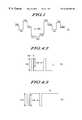
- the dynamic type of DC offsetsare more critical in zero IF baseband receivers. Dynamic offsets result from the same LO leakage described with respect to the static DC offsets. However, in the case of TDMA receivers, the LO leakage signal which appears at the RF port of the mixer can vary from timeslot to timeslot, producing a DC offset waveform at the output of the receiver as shown in FIG. 1 . As shown, the desired I or Q channel information waveform rides on top of the dynamic DC offset waveform. Consequently, from the perspective of any individual timeslot (TS0-TS7), there is a non zero DC offset above or below the 0 VDC reference voltage. Although AC coupled, the receiver typically has no way to reject this waveform.
- a GSM type cellular TDMA systemhas a timeslot duration of approximately 600 microseconds.
- the generated dynamic DC offset waveformmay have an effective frequency of less than 1 KHz. This waveform easily passes through the typical 90 KHz low pass filter response of the GSM baseband stages.
- the magnitude and phase of the LO vestige signals present at an RF port of the mixeris a function of gains and reflection coefficients throughout the IF portion of the receiver.
- AGCgain
- the problemis compounded by the fact that the gain settings for a given timeslot are also time variant as the mobile transmitting units move closer and further from the base station and as call traffic comes and goes. Therefore, the dynamic DC offset wave not only changes from timeslot to timeslot, but also from frame to frame.
- the presence of dynamic DC offset voltages as visible to a detector stage of a receiverhas been shown to degrade BER performance.
- a zero IF TDMA base station receivershould have a combined I channel DC offset and Q channel DC offset of less than 3% of the full scale input of an A/D converter that converts the analog signal to digital signal for the detector.
- the DC offsetcan produce less than 0.5 dB degradation of BER performance, hence, it would be desirable to remove or substantially reduce the undesirable dynamic DC offset prior to channel equalization to reduce BER.
- Conventional DC offset correction methodsgenerally include placing the LO signal trace on one side of a circuit board and placing the IF signal trace on another side of the PC board to help reduce the radiation impact of the signals.
- metal shieldingis typically placed around the LO to further help isolate the LO radiation from interfering with other receiver circuitry. Such methods can not typically be applied to integrated circuits due to the small size and location of the signal traces on the IC and other factors, particularly when the quadrature down converter and baseband circuitry is on one integrated circuit.
- Another method of reducing DC offsetsis to lower the IF frequency prior to the baseband stage through a triple conversion receiver where three IF stages (including the baseband stage) are used and the IF stage prior to the baseband stage has a lower LO frequency because it has been scaled down.
- the LO signalmay be at a lower frequency thereby being less prone to radiation, which in turn causes less offset.
- triple conversion filtersrequires additional components on an integrated circuit and adds complexity resulting in higher costs.
- FIG. 1is an illustration showing the effects of dynamic DC offsets in a TDMA base station receiver having a zero IF receiver
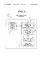
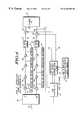
- FIG. 2is a block diagram generally depicting a cellular TDMA base station zero IF receiver with DC offset correction in accordance with one embodiment of the invention
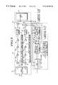
- FIG. 3is a block diagram depicting in more detail the embodiment of the cellular TDMA base station zero IF receiver with DC offset correction shown in FIG. 2;
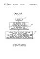
- FIG. 4.1is a flow diagram generally depicting the operation of the predictive DC offset correction stage of the cellular TDMA base station receiver shown in FIG. 2;
- FIGS. 4.2 and 4 . 3graphically illustrate a method for determining a component of a receiver calibration correction value in accordance with one embodiment of the invention
- FIG. 5is a general flow diagram depicting the steps carried out by a digital signal processor in the cellular TDMA base station zero IF receiver with DC offset correction to perform closed loop DC offset correction in accordance with the invention
- FIG. 6is a block diagram generally depicting another embodiment of the invention using only predictive DC offset correction as the basis for correcting for dynamic DC offset;
- FIG. 7is another embodiment of the invention utilizing a closed loop DC offset correction block as the basis for removing dynamic DC offset.
- the disclosed cellular TDMA base station receiver having an AC coupled baseband receivercorrects for the dynamic DC offsets by utilizing an open loop predictive signal processing method to respond instantly to changes in AGC settings on a timeslot by timeslot basis.
- the systemtakes into account not only an automatic gain control state of a timeslot of interest, but predicts DC offset as a function of all other AGC states of all timeslots in the frame.
- the base station receivermay also, if desired utilize separately or in combination, a closed loop error correction method that may be slower than the open loop predictive method, but can reduce the BER degradation or substantially cancel residual error left by the open loop predictive method when used in combination with the open loop predictive method.
- the closed loop error correctionaverages DC offset of a given timeslot over a series of frames to determine residual undesired DC offset and continually corrects for the detected DC offset accordingly.
- the disclosed TDMA base station receivermay find particular use in cellular TDMA base station zero-IF receivers, but it may be used in any suitable RF TDMA based system.
- FIG. 2shows a cellular TDMA base station receiver 10 with DC offset correction having a zero IF quadrature down converter and baseband integrated circuit (IC) 12 for receiving cellular TDMA frames, such as GSM formatted frames, through antenna 14 .
- the receiver 10is shown for one receiver branch. The receiver 10 shown would be duplicated for a diversity receiver.
- the cellular TMDA base station receiver 10also includes digital signal processor IC 16 , such as a Motorola Inc. DSP model number 56305, that has a predictive DC offset correction stage 18 and a closed loop DC offset correction stage 20 .
- the cellular TDMA base station receiver 10also includes memory 22 for storing receiver calibration offset data representing a receiver calibration offset voltage value in the form of two calibration look-up tables. One look-up table contains I channel receiver calibration offset data 24 and the other look-up table contains Q channel calibration offset data 26 . Each entry in a table corresponds to a different automatic gain control (AGC) setting for a given timeslot in a frame.
- AGCautomatic gain control
- the predictive DC offset correction stage 18predicts a predictive DC offset correction value for a selected timeslot using not only the stored receiver calibration data 24 and 26 corresponding to an automatic gain control (AGC) state of the selected timeslot, but also using an average of stored calibration offset data corresponding to AGC states for all timeslots in a given frame. Therefore, where a frame includes eight timeslots, the predictive DC offset correction stage determines the predictive DC offset prediction value for one timeslot as a function of AGC settings for the remaining seven timeslots. This dynamic DC offset correction prediction is done for each timeslot.
- AGCautomatic gain control
- the closed loop DC offset correction stage 20provides a closed loop DC correction value on a per timeslot basis by determining a combined DC offset value consisting of a natural DC offset level and an undesired DC offset level for the selected timeslot and by determining the undesired DC offset level by averaging the combined DC offset value for the selected timeslot over a number of frames to facilitate correction for detected DC offsets.
- the closed loop DC offset correction stage 20utilizes GSM type formats where a natural DC offset of a same timeslot over a range of frames is zero even though the natural offset for one timeslot may be non-zero.
- the predictive DC offset correction stage 18serves as an open loop dynamic DC offset correction circuit and the closed loop DC offset correction stage 20 serves as a closed loop correction stage to remove residual offset components not fully eliminated by the predictive DC offset correction stage 18 .
- any non-zero result from long term averaging by the closed loop DC offset correction stage 20is subtracted from corrected received data prior to demodulation.
- the receiver calibration correction data 24 for the received in-phase channel datais receiver calibration offset voltage values for each automatic gain control state determined relative to a known reference value for an in-phase signal.
- the receiver calibration correction data 26 for the received quadrature channel datais preferably receiver calibration offset voltage values for each automatic gain control state determined relative to a known reference value for a quadrature signal.
- Memory 22may be any suitable non-volatile memory.
- FIG. 3shows in more detail, the zero IF quadrature down converter and baseband IC 12 having conventional baseband in-phase channel mixing circuit 30 and a baseband quadrature phase channel mixing circuit 32 each coupled to receive and mix a local oscillator (LO) frequency signal 34 output by local oscillator circuit 36 .
- the baseband in-phase channel mixing circuit, the baseband quadrature phase mixing circuit and the local oscillatorare all located on the same integrated circuit.
- the IF frequencyis 167 MHz and the local oscillator frequency 34 is also 167 MHz thereby creating a zero IF receiver with a relatively high IF frequency.
- the LO generatorcan be any suitable frequency.
- the zero IF quadrature down converter and baseband IC 12is preferably a dual conversion type receiver to minimize complexity and cost. However, it will be recognized that a triple conversion receiver or other configuration may also be used if desired.
- the mixing circuits 30 and 32also receive the phase adjusted RF signals from quadrature splitter 38 as known in the art.
- An AGC controlled variable gain amplifier 39provides the quadrature splitter 38 with an amplified received signal also as known in the art.
- LO leakagecan enter an input of the amplifier 39 causing dynamic DC variations between timeslots depending on the gain of the amplifier 39 for a given timeslot.
- the zero IF quadrature down converter and baseband IC 12also includes a series of gain stages 40 A through 40 F. Between the gain stages 40 A- 40 F are a series of static DC offset correction networks indicated as 42 and 44 . The static offsets are addressed by the offset correction networks 42 and 44 as known in the art. By virtue of the offset correction networks 42 and 44 , the zero IF quadrature down converter and baseband IC 12 is an AC coupled receiver.
- the I channel data output from the gain stages 40 A through 40 Cserves as input data to an 8 bit analog to digital (A/D) converter 46 as known in the art.
- the I channel data output from the gain stages 40 D through 40 Fhaving been passed through the static DC offset collection network 44 , serves as Q channel data input to another 8 bit A/D 48 as also known in the art.
- Uncorrected baseband I and Q channel digitized signals 50 and 52 output from the A/D converters 46 and 48is corrected for dynamic DC offset voltages through summing network 54 and 56 respectively.
- Resulting DC offset corrected baseband digitized signals 58 and 60serve as input signal data to a channel equalizer 70 where conventional signal processing is performed to determine the information received through the quadrature down converter and baseband IC 12 .
- the channel equalizer 70is a conventional equalizer and includes a matched filter and MLSE Viterbi algorithm.
- AGC controller 72samples the DC offset corrected baseband digitized signal 58 for the I channel and the DC offset corrected baseband digitized signal 60 for the Q channel to determine the proper automatic gain control for the variable gain amplifier 39 on a per timeslot basis.
- the AGC control valueis based on the power level at the channel equalizer 70 input (I2+Q2)1/2, and is performed independently for each timeslot.
- the AGC controller 72attempts to maintain the mean value of the received signal at one half of the A/D converter full scale.
- the AGC controller 72will integrate the short term Rayleigh variation, as it follows the long term log-normal variation.
- the I and Q inputs, of DC offset corrected baseband digitized signals 58 and 60 to the AGC algorithmare taken after the I and Q composite correction values 86 and 88 are applied.
- the AGC controller settingsare retrieved by the predictive DC offset correction stage 18 .
- the predictive DC offset correction stage 18also receives the I channel and Q channel DC offset calibration values 24 and 26 from the lookup tables to determine predictive offset correction values 74 for each timeslot of the I channel and predictive offset correction values 76 for each timeslot of the Q channel.
- the closed loop DC offset correction stage 20receives the corrected baseband I and Q channel digitized signals 58 and 60 and analyzes the corrected baseband I and Q channel digitized signals 58 and 60 for the combined natural and undesired dynamic DC components.
- the natural DC offsetrefers to the inherent, non-zero, DC value of the burst or timeslot.
- the GSM systemas a GMSK based system, has these characteristics. It has been found that with random modulation, there is greater than 40% probability that the natural DC offset (of I or Q) will exceed 1.5% of full scale. To remove the natural offset would have the same degradation affects as adding an erroneous offset of equal amplitude. Therefore, a viable DC offset solution should have the ability to distinguish between the natural DC offsets, and the undesired DC offsets, and remove only the undesired term.
- the closed loop DC offset correction stage 20generates an I channel closed loop DC correction value 78 and also generates a Q channel closed loop DC correction value 80 on a per timeslot basis.
- the combination of these I and Q closed loop DC correction values 78 and 80may be considered to be a closed loop DC correction vector.
- An I channel DC correction value summing stage 82sums the predictive DC offset correction value 74 with closed loop DC correction value 78 on a per timeslot basis to generate an I channel composite offset correction value 86 .
- the closed loop DC correction value 78is determined by averaging the same timeslot over a series of eight or ten frames.
- DC offset correction value summer 84sums the Q channel predictive offset correction value 76 with the closed loop DC correction value 80 to generate a Q channel composite offset correction value 88 .
- the Q channel summer 56receives the composite offset correction value 88 and subtracts the composite offset correction value 88 from the uncorrected Q channel baseband digitized signal 52 to generate the Q channel DC offset corrected baseband digitized signal 60 .
- summer 54receives the I channel composite offset correction value 86 and subtracts this value from the uncorrected baseband I channel digitized signal 50 to generate the DC offset corrected baseband digitized signal 58 for use by the channel equalizer 70 .
- all signal processing tasksare performed by the same digital signal processor 16 which performs channel equalization. However, a separate processor may be used if desired.
- the receiver 10is powered up during the manufacturing process as shown in block 100 .
- the DSP 16operates to determine and store the receiver calibration correction data 24 and 26 in the tables. This calibration data is taken at room temperature. Consequently, the predictive DC offset correction stage may be susceptible to some error resulting from temperature drift. The closed loop DC offset correction stage compensates for this residual error.
- the receiver 10may also be modified to evaluate temperature increases from a thermal monitoring device in the base station. In this way, the receiver 10 can automatically provide additional dynamic DC offset correction.
- the DSP 16generates the predictive DC offset correction values 74 and 76 by first obtaining I channel and Q channel calibration table data stored in memory 22 . This is shown in block 102 .
- the DSP 16obtains receiver calibration offset data 24 and 26 , representing a receiver calibration offset voltage value for each automatic gain control state for I channel and Q channel determined to a relative known reference value, by setting 7 AGC settings to full gain and measuring an output of the DC voltage at the A /D 46 and 48 of the 8th slot. This is shown in block 102 A.
- the DSPmeasures and stores the voltage difference between each AGC setting, and the reference setting.
- the reference settingis preferably full gain.
- the DSPconfigures seven of the eight timeslots at the reference setting (full gain).
- the DSPthen configures the 8th timeslot at the AGC setting to be calibrated (n).
- a DC offset waveformwill be produced in both I and Q channel.
- the DC voltage value of the 8th timeslotis measured by the channel equalizer 70 by averaging several samples per timeslot over multiple successive frames.
- the peak voltage value measured from a 0 V reference(or other suitable reference voltage) serves as the base for determining the calibration offset data.
- the DC value V(n) of the eighth timeslotis ⁇ fraction (8/7) ⁇ ths of the DC offset waveform. Therefore, it is ⁇ fraction (8/7) ⁇ ths of the DC value of the eighth timeslot voltage which is stored in the calibration table for this AGC setting.
- Vni and Vnqdenote the offset voltage values which are stored for the nth AGC state, for I and Q respectively.
- the Vni and Vnqcan have either a positive, or negative value. This calibration process is repeated for each of the AGC settings as shown in block 102 b.
- the receiver calibration offset voltage valuesare stored after being measured for each AGC setting as a separate I channel table and as a separate Q channel table in memory 22 .
- the receiver calibration offset data stored in non-volatile memory 22 as tables,is accessed every timeslot by the DSP 16 and used to calculate the appropriate dynamic predictive DC offset correction value 74 and 76 .
- the tableconsists of offset values, corresponding to each possible AGC state. An example of the data in the tables is shown below in columns (a), (b) and (c) where columns (a) and (b) form the I table and columns (a) and (c) form the Q table.
- receiver calibration offset voltage values (columns (b) and (c)) stored in the I table and Q tablesbe interpolated for the first 30 dB range of AGC settings. Thereafter the remaining receiver calibration offset voltage values may be extrapolated from selected measurements to save time during the manufacturing process. For each frame, (N), each of the eight timeslots have corresponding AGC settings, and calibration parameters, as above.
- the AGC controller 72determines the AGC settings for each timeslot in a current frame as shown in block 104 .
- the predictive DC offset correction stage 18retrieves the DC offset values corresponding to that AGC setting from the I and Q tables as shown in block 106 .
- the predictive DC offset correction stage 18then separately determines the predicted DC offset correction values 74 and 76 (undesired offset values for I and Q channel).
- the DC offsetsare produced from a linear process, and therefore, superposition can be applied to describe and predict the composite DC output waveform.
- the DC offset correction networks 42 and 44 ACcouple the gain stages, it is only the apparent DC voltage for any one timeslot that can be non-zero.
- Ipredict(ts)is the predicted DC offset in the I channel for the (ts) timeslot.
- Qpredict(ts)is the predicted DC offset in the Q channel for the (ts) timeslot.
- Ioffset(ts)is the stored receiver calibration offset data (offset voltage value) for the I channel corresponding to the (ts) timeslot.
- Qoffset(ts)is the stored receiver calibration offset data (offset voltage value) for the Q channel corresponding to the (ts) timeslot.
- Ioffset(x)is the stored receiver calibration offset data for the I channel corresponding to each of the 8 timeslots (x between zero and 7).
- Qoffset(x)is the stored receiver calibration offset data for the Q channel corresponding to each of the 8 timeslots (x between zero and 7).
- FIG. 5shows the steps used by the closed loop DC offset correction stage 20 which examines the long term DC value of each timeslot, over the course of multiple TDMA frames.
- the long term averageshould approach zero. Therefore, any deviation from zero is used to augment the correction values determined by the predictive DC offset correction stage 18 .
- the closed loop DC offset correction stage 20samples the corrected baseband I and Q channel digitized signals 58 and 60 as shown in block 114 .
- the DC offset correction stage 20under control of the DSP 16 , measures a combined DC offset value consisting of both the natural DC offset level and undesired DC offset level over a given timeslot by taking 500 samples of the signal for each timeslot.
- offsets in I and Q channelsare independent. Offsets in consecutive TDMA frames (for a given timeslot) are not independent; this results from the significant deterministic content of the GSM burst (midamble, tail bits, etc.).
- the magnitude of the DC offsetsfollow a Gaussian distribution, and are essentially bounded by +12% of full scale. Where corrected baseband I and Q channel digitized signal 58 and 60 are independently averaged over eight consecutive bursts, there is 90% confidence that the average value of I+Q is less than 1.5% of full scale. This figure is generally considered acceptably close to zero. Therefore, averaging over 8-10 TDMA frames is recommended. This will permit convergence in 8 TDMA frames (one speech frame) and will help insure (with 90% confidence) less than 1.5% residual DC offset.
- the closed loop DC offset correction stage 20determines the combined DC offset value by determining the undesired DC offset level by averaging the combined DC offset value for the selected timeslot over a plurality of frames. If the average combined DC offset value for the same timeslot is zero, then there is only natural DC offset and no undesired term exists. If the combined DC offset value is not zero, then an undesired DC offset exists and this amount is added to the predictive DC offset value 74 or 76 respectively. In this way, the summers 80 and 82 provide a composite offset correction value 86 and 88 by summing the predictive DC correction value 74 and the closed loop DC correction value 76 on a timeslot by timeslot basis to obtain a composite DC offset correction value 86 and 88 . Where no predictive DC offset correction stage 18 is used, the DSP 16 subtracts the undesired amount from each of the 500 samples.
- DC offsets for a given timeslotare predicted by the disclosed receiver.
- the predictionis based on calibration data pertaining to the timeslot in question, and also the conditions pertaining to each of the other seven timeslots in the TDMA frame.
- the receiveralso utilizes information about the inherent or natural DC value of a TDMA timeslot, or GSM burst, by taking into account the finding that a timeslot may have a non-zero DC offset but the long term average of consecutive bursts is zero.
- FIG. 6shows a receiver using only the predictive DC offset correction block 18 without the closed loop DC offset correction stage 20 .
- the predicted DC offset valuesare subtracted from the uncorrected baseband I channel digitized signal 50 and the uncorrected baseband Q channel digitized signal 52 (see FIG. 6) by the DSP 16 .
- the correction values determined by the closed loop correction stage 20are also subtracted from the uncorrected baseband I channel digitized signal 50 and the uncorrected baseband Q channel digitized signal 52 .
- FIG. 7is another embodiment of a receiver using only the closed loop DC offset correction stage 20 for correcting for the dynamic DC offset.
- the closed loop DC offset valuesare subtracted from the uncorrected baseband I channel digitized signal 50 and the uncorrected baseband Q channel digitized signal 52 by the DSP 16 .
Landscapes
- Engineering & Computer Science (AREA)
- Power Engineering (AREA)
- Computer Networks & Wireless Communication (AREA)
- Signal Processing (AREA)
- Digital Transmission Methods That Use Modulated Carrier Waves (AREA)
Abstract
Description
| (a) | (b) | (c) | |
| Timeslot | AGC State | Ioffset (from cal) | Qoffset (from cal) |
| 0 | n0 | Vn0I | Vn0Q |
| 1 | n1 | Vn1I | Vn1Q |
| 2 | n2 | Vn2I | Vn2Q |
| 3 | n3 | Vn3I | Vn3Q |
| 4 | n4 | Vn4I | Vn4Q |
| 5 | n5 | Vn5I | Vn5Q |
| 6 | n6 | Vn6I | Vn6Q |
| 7 | n7 | Vn7I | Vn7Q |

Claims (10)
Priority Applications (1)
| Application Number | Priority Date | Filing Date | Title |
|---|---|---|---|
| US08/904,398US6240100B1 (en) | 1997-07-31 | 1997-07-31 | Cellular TDMA base station receiver with dynamic DC offset correction |
Applications Claiming Priority (1)
| Application Number | Priority Date | Filing Date | Title |
|---|---|---|---|
| US08/904,398US6240100B1 (en) | 1997-07-31 | 1997-07-31 | Cellular TDMA base station receiver with dynamic DC offset correction |
Publications (1)
| Publication Number | Publication Date |
|---|---|
| US6240100B1true US6240100B1 (en) | 2001-05-29 |
Family
ID=25419083
Family Applications (1)
| Application Number | Title | Priority Date | Filing Date |
|---|---|---|---|
| US08/904,398Expired - LifetimeUS6240100B1 (en) | 1997-07-31 | 1997-07-31 | Cellular TDMA base station receiver with dynamic DC offset correction |
Country Status (1)
| Country | Link |
|---|---|
| US (1) | US6240100B1 (en) |
Cited By (56)
| Publication number | Priority date | Publication date | Assignee | Title |
|---|---|---|---|---|
| US20020048267A1 (en)* | 2000-10-19 | 2002-04-25 | Interdigital Technology Corporation | Selectively activated AGC signal measurement unit |
| US6381260B1 (en)* | 1997-10-17 | 2002-04-30 | Siemens Aktiengesellschaft | Method and radio station for data transmission |
| US20020123320A1 (en)* | 2001-01-02 | 2002-09-05 | Layne Lisenbee | Apparatus and method for canceling DC offset in communications signals |
| US6459889B1 (en)* | 2000-02-29 | 2002-10-01 | Motorola, Inc. | DC offset correction loop for radio receiver |
| US20030021333A1 (en)* | 2001-07-26 | 2003-01-30 | Luca Blessent | Noise gain control |
| US6539215B1 (en)* | 1999-05-27 | 2003-03-25 | Sony Corporation | Down converter and demodulator using a three port junction |
| US20030064697A1 (en)* | 2001-09-28 | 2003-04-03 | Twomey Gerald J. | Analog baseband signal processing system and method |
| US6556635B1 (en)* | 1999-11-09 | 2003-04-29 | Lsi Logic Corporation | Communications receiver having adaptive dynamic range |
| US6654593B1 (en)* | 2000-10-30 | 2003-11-25 | Research In Motion Limited | Combined discrete automatic gain control (AGC) and DC estimation |
| WO2003044949A3 (en)* | 2001-11-16 | 2004-02-12 | Renesas Tech Corp | A communication semiconductor integrated circuit device and a wireless communication system |
| US20040053596A1 (en)* | 2001-01-09 | 2004-03-18 | Lars Svensson | Radio receiver |
| US6753727B2 (en)* | 2002-06-13 | 2004-06-22 | Skyworks Solutions, Inc. | Sequential DC offset correction for amplifier chain |
| US20040176055A1 (en)* | 2003-03-03 | 2004-09-09 | Nokia Corporation | Method and apparatus for compensating DC level in an adaptive radio receiver |
| US20040198261A1 (en)* | 2002-06-28 | 2004-10-07 | Wei Xiong | Method of self-calibration in a wireless transmitter |
| US20040247046A1 (en)* | 2003-06-09 | 2004-12-09 | Yung-Sheng Hsiao | Device for wlan baseband processing with dc offset reduction |
| WO2005002074A1 (en)* | 2003-06-06 | 2005-01-06 | Interdigital Technology Corporation | Method and system for continuously compensating for phase variations introduced into a communication signal by automatic gain control adjustments |
| US20050009493A1 (en)* | 2003-06-17 | 2005-01-13 | Baoguo Yang | DC offset correction for very low intermediate frequency receiver |
| US20050020226A1 (en)* | 2002-09-05 | 2005-01-27 | Rishi Mohindra | DC offset cancellation in a zero if receiver |
| US20050026584A1 (en)* | 2003-08-01 | 2005-02-03 | Michael Lewis | Low-latency DC compensation |
| US6868128B1 (en)* | 2000-07-05 | 2005-03-15 | Rfmd Wpan, Inc. | Method and apparatus for calibrating DC-offsets in a direct conversion receiver |
| US20050056334A1 (en)* | 2003-09-17 | 2005-03-17 | Groz-Beckert Kg | Shaft drive system for power loom shafts |
| EP1517440A3 (en)* | 2003-09-16 | 2005-06-15 | Sony Ericsson Mobile Communications Japan, Inc. | Variable gain control circuit and receiver apparatus using the circuit |
| US20050141656A1 (en)* | 2003-11-22 | 2005-06-30 | Lg Electronics Inc. | Apparatus and method for enhancing a reception rate of a receiver |
| US20050208916A1 (en)* | 2001-02-16 | 2005-09-22 | Peterzell Paul E | Direct conversion receiver architecture |
| US20050239428A1 (en)* | 2004-04-13 | 2005-10-27 | Maxlinear, Inc. | Dual conversion receiver with programmable intermediate frequency and channel selection |
| US20050277396A1 (en)* | 2004-06-09 | 2005-12-15 | Spyros Pipilos | Apparatus and methods for eliminating DC offset in a wireless communication device |
| US20060045206A1 (en)* | 2004-08-30 | 2006-03-02 | Brent Keeth | Method and system for generating reference voltages for signal receivers |
| US20060079193A1 (en)* | 2003-07-25 | 2006-04-13 | Tadahiro Sato | Radio receiver and gain control method |
| US20060078069A1 (en)* | 2004-10-12 | 2006-04-13 | Maxlinear, Inc. | Hybrid receiver architecture using upconversion followed by direct downconversion |
| US20060083335A1 (en)* | 2004-10-12 | 2006-04-20 | Maxlinear, Inc. | Receiver architecture with digitally generated intermediate frequency |
| US7065164B1 (en)* | 2000-07-17 | 2006-06-20 | Mitsubishi Denki Kabushiki Kaisha | Automatic gain control and wireless communication device |
| US20060189290A1 (en)* | 2000-09-18 | 2006-08-24 | Broadcom Corporation | Direct conversion tuner |
| US20060199552A1 (en)* | 2005-03-02 | 2006-09-07 | Cisco Technology, Inc. | Method and system for self-calibrating transmit power |
| US20060222117A1 (en)* | 2005-04-04 | 2006-10-05 | Mahibur Rahman | DC offset correction system for a receiver with baseband gain control |
| US20060280268A1 (en)* | 2005-06-14 | 2006-12-14 | Freescale Semiconductor, Inc. | DC offset correction for constant envelope signals |
| US20070072571A1 (en)* | 2005-09-28 | 2007-03-29 | Runhua Sun | DC offset cancellation circuit for a receiver |
| US20070230622A1 (en)* | 2006-03-31 | 2007-10-04 | Joseph Brian C | UWB radio interface with DC offset |
| US20070242599A1 (en)* | 2006-04-14 | 2007-10-18 | Freescale Semiconductor Inc | Mitigation of DC distortion in OFDM receivers |
| US20070259638A1 (en)* | 2006-05-06 | 2007-11-08 | Jae-Wan Kim | Elimination of DC offset in analog baseband circuit with minimized transients |
| US20070275678A1 (en)* | 2006-04-07 | 2007-11-29 | Rohde & Schwarz Gmbh & Co. Kg | Method and Apparatus for Leveling an Increasing or Decreasing Slope of an AM Modulated Receiving Signal |
| US20070293180A1 (en)* | 2006-06-14 | 2007-12-20 | Freescale Semiconductor, Inc. | DC offset correction for direct conversion receivers |
| US20080270170A1 (en)* | 2002-07-18 | 2008-10-30 | Parkervision, Inc. | Networking Methods and Systems |
| CN100431273C (en)* | 2003-06-06 | 2008-11-05 | 美商内数位科技公司 | Communication device for continuously compensating phase variations of an incoming communication signal |
| US20080293369A1 (en)* | 2007-05-22 | 2008-11-27 | Atmel Germany Gmbh | Signal processing device and signal processing method |
| US20090264090A1 (en)* | 2008-04-21 | 2009-10-22 | Freescale Semiconductor, Inc. | Dc offset calibration in a direct conversion receiver |
| US20100003943A1 (en)* | 2004-12-10 | 2010-01-07 | Maxlinear, Inc. | Harmonic Reject Receiver Architecture and Mixer |
| US20100086086A1 (en)* | 2001-11-09 | 2010-04-08 | Parkervision, Inc. | Gain control in a communication channel |
| US20100144303A1 (en)* | 2008-12-05 | 2010-06-10 | Motorola, Inc. | Method and apparatus for removing dc offset in a direct conversion receiver |
| US20110151979A1 (en)* | 2009-12-23 | 2011-06-23 | Aristocrat Technologies Australia Pty Limited | Method of enabling restoration of games and a method of restoring games |
| US8340618B2 (en) | 1998-10-21 | 2012-12-25 | Parkervision, Inc. | Method and system for down-converting an electromagnetic signal, and transforms for same, and aperture relationships |
| US8396173B2 (en) | 2007-10-01 | 2013-03-12 | Maxlinear, Inc. | I/Q calibration techniques |
| US8406724B2 (en) | 1998-10-21 | 2013-03-26 | Parkervision, Inc. | Applications of universal frequency translation |
| US8571135B2 (en) | 1999-04-16 | 2013-10-29 | Parkervision, Inc. | Method, system and apparatus for balanced frequency up-conversion of a baseband signal |
| US8588725B2 (en) | 2000-04-14 | 2013-11-19 | Parkervision, Inc. | Apparatus, system, and method for down converting and up-converting electromagnetic signals |
| US8594228B2 (en) | 1999-04-16 | 2013-11-26 | Parkervision, Inc. | Apparatus and method of differential IQ frequency up-conversion |
| US10310999B2 (en)* | 1999-10-19 | 2019-06-04 | Rambus Inc. | Flash memory controller with calibrated data communication |
Citations (3)
| Publication number | Priority date | Publication date | Assignee | Title |
|---|---|---|---|---|
| US5204977A (en)* | 1991-04-01 | 1993-04-20 | Motorola, Inc. | Apparatus and method of automatic gain control in a receiver |
| US5212826A (en)* | 1990-12-20 | 1993-05-18 | Motorola, Inc. | Apparatus and method of dc offset correction for a receiver |
| US5422889A (en)* | 1992-10-28 | 1995-06-06 | Alcatel N.V. | Offset correction circuit |
- 1997
- 1997-07-31USUS08/904,398patent/US6240100B1/ennot_activeExpired - Lifetime
Patent Citations (3)
| Publication number | Priority date | Publication date | Assignee | Title |
|---|---|---|---|---|
| US5212826A (en)* | 1990-12-20 | 1993-05-18 | Motorola, Inc. | Apparatus and method of dc offset correction for a receiver |
| US5204977A (en)* | 1991-04-01 | 1993-04-20 | Motorola, Inc. | Apparatus and method of automatic gain control in a receiver |
| US5422889A (en)* | 1992-10-28 | 1995-06-06 | Alcatel N.V. | Offset correction circuit |
Cited By (126)
| Publication number | Priority date | Publication date | Assignee | Title |
|---|---|---|---|---|
| US6381260B1 (en)* | 1997-10-17 | 2002-04-30 | Siemens Aktiengesellschaft | Method and radio station for data transmission |
| US8340618B2 (en) | 1998-10-21 | 2012-12-25 | Parkervision, Inc. | Method and system for down-converting an electromagnetic signal, and transforms for same, and aperture relationships |
| US8660513B2 (en) | 1998-10-21 | 2014-02-25 | Parkervision, Inc. | Method and system for down-converting an electromagnetic signal, and transforms for same, and aperture relationships |
| US8594607B2 (en) | 1998-10-21 | 2013-11-26 | Parkervision, Inc. | Methods and systems for down-converting a signal using a complementary transistor structure |
| US8406724B2 (en) | 1998-10-21 | 2013-03-26 | Parkervision, Inc. | Applications of universal frequency translation |
| US8594228B2 (en) | 1999-04-16 | 2013-11-26 | Parkervision, Inc. | Apparatus and method of differential IQ frequency up-conversion |
| US8571135B2 (en) | 1999-04-16 | 2013-10-29 | Parkervision, Inc. | Method, system and apparatus for balanced frequency up-conversion of a baseband signal |
| US6539215B1 (en)* | 1999-05-27 | 2003-03-25 | Sony Corporation | Down converter and demodulator using a three port junction |
| US10310999B2 (en)* | 1999-10-19 | 2019-06-04 | Rambus Inc. | Flash memory controller with calibrated data communication |
| US6556635B1 (en)* | 1999-11-09 | 2003-04-29 | Lsi Logic Corporation | Communications receiver having adaptive dynamic range |
| US6459889B1 (en)* | 2000-02-29 | 2002-10-01 | Motorola, Inc. | DC offset correction loop for radio receiver |
| US8588725B2 (en) | 2000-04-14 | 2013-11-19 | Parkervision, Inc. | Apparatus, system, and method for down converting and up-converting electromagnetic signals |
| US6868128B1 (en)* | 2000-07-05 | 2005-03-15 | Rfmd Wpan, Inc. | Method and apparatus for calibrating DC-offsets in a direct conversion receiver |
| US7065164B1 (en)* | 2000-07-17 | 2006-06-20 | Mitsubishi Denki Kabushiki Kaisha | Automatic gain control and wireless communication device |
| US7636558B2 (en)* | 2000-09-18 | 2009-12-22 | Broadcom Corporation | Direct conversion tuner |
| US20060189290A1 (en)* | 2000-09-18 | 2006-08-24 | Broadcom Corporation | Direct conversion tuner |
| US20100093295A1 (en)* | 2000-09-18 | 2010-04-15 | Broadcom Corporation | Direct conversion tuner |
| US8467755B2 (en) | 2000-09-18 | 2013-06-18 | Broadcom Corporation | Direct conversion tuner |
| US20020048267A1 (en)* | 2000-10-19 | 2002-04-25 | Interdigital Technology Corporation | Selectively activated AGC signal measurement unit |
| US7085255B2 (en)* | 2000-10-19 | 2006-08-01 | Interdigital Technology Corporation | Selectively activated AGC signal measurement unit |
| US20060229044A1 (en)* | 2000-10-30 | 2006-10-12 | Sean Simmons | Combined discrete automatic gain control (AGC) and DC estimation |
| US20040053586A1 (en)* | 2000-10-30 | 2004-03-18 | Sean Simmons | Combined discrete automatic gain control (AGC) and DC estimation |
| US7295823B2 (en) | 2000-10-30 | 2007-11-13 | Research In Motion Limited | Combined discrete automatic gain control (AGC) and DC estimation |
| US7062243B2 (en) | 2000-10-30 | 2006-06-13 | Research In Motion Limited | Combined discrete automatic gain control (AGC) and DC estimation |
| US6654593B1 (en)* | 2000-10-30 | 2003-11-25 | Research In Motion Limited | Combined discrete automatic gain control (AGC) and DC estimation |
| US20080043887A1 (en)* | 2000-10-30 | 2008-02-21 | Sean Simmons | Combined discrete automatic gain control (agc) and dc estimation |
| US7653369B2 (en) | 2000-10-30 | 2010-01-26 | Research In Motion Limited | Combined discrete automatic gain control (AGC) and DC estimation |
| US6907235B2 (en)* | 2001-01-02 | 2005-06-14 | Texas Instruments Incorporated | Apparatus and method for canceling DC offset in communications signals |
| US20020123320A1 (en)* | 2001-01-02 | 2002-09-05 | Layne Lisenbee | Apparatus and method for canceling DC offset in communications signals |
| US20040053596A1 (en)* | 2001-01-09 | 2004-03-18 | Lars Svensson | Radio receiver |
| US20080014895A1 (en)* | 2001-02-16 | 2008-01-17 | Qualcomm Incorporated | Direct conversion receiver architecture |
| US8626099B2 (en) | 2001-02-16 | 2014-01-07 | Qualcomm Incorporated | Direct conversion receiver architecture |
| US8634790B2 (en) | 2001-02-16 | 2014-01-21 | Qualcomm Incorporated | Direct conversion receiver architecture with digital fine resolution variable gain amplification |
| US20050208916A1 (en)* | 2001-02-16 | 2005-09-22 | Peterzell Paul E | Direct conversion receiver architecture |
| US8615212B2 (en)* | 2001-02-16 | 2013-12-24 | Qualcomm Incorporated | Direct conversion receiver architecture |
| US6947472B2 (en)* | 2001-07-26 | 2005-09-20 | Qualcomm Incorporated | Noise gain control |
| US20030021333A1 (en)* | 2001-07-26 | 2003-01-30 | Luca Blessent | Noise gain control |
| US7027791B2 (en)* | 2001-09-28 | 2006-04-11 | International Business Machines Corporation | Analog baseband signal processing system and method |
| US20030064697A1 (en)* | 2001-09-28 | 2003-04-03 | Twomey Gerald J. | Analog baseband signal processing system and method |
| US8446994B2 (en)* | 2001-11-09 | 2013-05-21 | Parkervision, Inc. | Gain control in a communication channel |
| US20100086086A1 (en)* | 2001-11-09 | 2010-04-08 | Parkervision, Inc. | Gain control in a communication channel |
| WO2003044949A3 (en)* | 2001-11-16 | 2004-02-12 | Renesas Tech Corp | A communication semiconductor integrated circuit device and a wireless communication system |
| US20050107056A1 (en)* | 2001-11-16 | 2005-05-19 | Akira Okasaka | Communication semiconductor integrated circuit device and a wireless communication system |
| WO2003107543A3 (en)* | 2002-06-13 | 2004-12-02 | Skyworks Solutions Inc | Sequential dc offset correction for amplifier chain |
| KR100976904B1 (en) | 2002-06-13 | 2010-08-18 | 스카이워크스 솔루션즈 인코포레이티드 | Sequential DC Offset Correction Method for Amplifier Chains |
| US6753727B2 (en)* | 2002-06-13 | 2004-06-22 | Skyworks Solutions, Inc. | Sequential DC offset correction for amplifier chain |
| US20040198261A1 (en)* | 2002-06-28 | 2004-10-07 | Wei Xiong | Method of self-calibration in a wireless transmitter |
| US20050159116A1 (en)* | 2002-06-28 | 2005-07-21 | Wei Xiong | Method of self-calibration in a wireless transmitter |
| US20080270170A1 (en)* | 2002-07-18 | 2008-10-30 | Parkervision, Inc. | Networking Methods and Systems |
| US8407061B2 (en) | 2002-07-18 | 2013-03-26 | Parkervision, Inc. | Networking methods and systems |
| US7110734B2 (en)* | 2002-09-05 | 2006-09-19 | Maxim Integrated Products Inc. | DC offset cancellation in a zero if receiver |
| US20060246842A1 (en)* | 2002-09-05 | 2006-11-02 | Maxim Integrated Products | DC offset cancellation in a zero IF receiver |
| US7532873B2 (en) | 2002-09-05 | 2009-05-12 | Maxim Integrated Products, Inc. | DC offset cancellation in a zero IF receiver |
| US20050020226A1 (en)* | 2002-09-05 | 2005-01-27 | Rishi Mohindra | DC offset cancellation in a zero if receiver |
| US7684775B2 (en)* | 2003-03-03 | 2010-03-23 | Nokia Corporation | Method and apparatus for compensating DC level in an adaptive radio receiver |
| US20040176055A1 (en)* | 2003-03-03 | 2004-09-09 | Nokia Corporation | Method and apparatus for compensating DC level in an adaptive radio receiver |
| US7139542B2 (en)* | 2003-03-03 | 2006-11-21 | Nokia Corporation | Method and apparatus for compensating DC level in an adaptive radio receiver |
| AU2004253071B2 (en)* | 2003-06-06 | 2007-05-24 | Interdigital Technology Corporation | Method and system for continuously compensating for phase variations introduced into a communication signal by automatic gain control adjustments |
| CN100431273C (en)* | 2003-06-06 | 2008-11-05 | 美商内数位科技公司 | Communication device for continuously compensating phase variations of an incoming communication signal |
| WO2005002074A1 (en)* | 2003-06-06 | 2005-01-06 | Interdigital Technology Corporation | Method and system for continuously compensating for phase variations introduced into a communication signal by automatic gain control adjustments |
| US20060183451A1 (en)* | 2003-06-06 | 2006-08-17 | Interdigital Technology Corporation | Method and system for continuously compensating for phase variations introduced into a communication signal by automatic gain control adjustments |
| US20040247046A1 (en)* | 2003-06-09 | 2004-12-09 | Yung-Sheng Hsiao | Device for wlan baseband processing with dc offset reduction |
| US7215722B2 (en) | 2003-06-09 | 2007-05-08 | Ali Corporation | Device for WLAN baseband processing with DC offset reduction |
| US7277688B2 (en)* | 2003-06-17 | 2007-10-02 | Broadcom Corporation | DC offset correction for very low intermediate frequency receiver |
| US20050009493A1 (en)* | 2003-06-17 | 2005-01-13 | Baoguo Yang | DC offset correction for very low intermediate frequency receiver |
| US7593705B2 (en)* | 2003-07-25 | 2009-09-22 | Fujitsu Limited | Radio receiver and gain control method |
| US20060079193A1 (en)* | 2003-07-25 | 2006-04-13 | Tadahiro Sato | Radio receiver and gain control method |
| US7313374B2 (en)* | 2003-08-01 | 2007-12-25 | Infineon Technologies Ag | Low-latency DC compensation |
| US20050026584A1 (en)* | 2003-08-01 | 2005-02-03 | Michael Lewis | Low-latency DC compensation |
| EP1517440A3 (en)* | 2003-09-16 | 2005-06-15 | Sony Ericsson Mobile Communications Japan, Inc. | Variable gain control circuit and receiver apparatus using the circuit |
| US7231195B2 (en) | 2003-09-16 | 2007-06-12 | Sony Ericsson Mobile Communications Japan, Inc. | Variable gain control circuit and receiver apparatus using the circuit |
| US20050056334A1 (en)* | 2003-09-17 | 2005-03-17 | Groz-Beckert Kg | Shaft drive system for power loom shafts |
| US20050141656A1 (en)* | 2003-11-22 | 2005-06-30 | Lg Electronics Inc. | Apparatus and method for enhancing a reception rate of a receiver |
| US7602865B2 (en) | 2003-11-22 | 2009-10-13 | Lg Electronics Inc. | Apparatus and method for enhancing a reception rate of a receiver |
| US20050239428A1 (en)* | 2004-04-13 | 2005-10-27 | Maxlinear, Inc. | Dual conversion receiver with programmable intermediate frequency and channel selection |
| US7532870B2 (en) | 2004-04-13 | 2009-05-12 | Maxlinear, Inc. | Method and apparatus for DC offset removal |
| US20110081877A1 (en)* | 2004-04-13 | 2011-04-07 | Maxlinear, Inc. | Dual conversion receiver with programmable intermediate frequency and channel selection |
| US8718584B2 (en) | 2004-04-13 | 2014-05-06 | Maxlinear, Inc. | Dual conversion receiver with programmable intermediate frequency and channel selection |
| US20050248478A1 (en)* | 2004-04-13 | 2005-11-10 | Maxlinear, Inc. | Method and apparatus for DC offset removal |
| US7778613B2 (en) | 2004-04-13 | 2010-08-17 | Maxlinear, Inc. | Dual conversion receiver with programmable intermediate frequency and channel selection |
| WO2005101671A3 (en)* | 2004-04-13 | 2006-01-12 | Maxlinear Inc | Method and apparatus for dc offset removal |
| US20050277396A1 (en)* | 2004-06-09 | 2005-12-15 | Spyros Pipilos | Apparatus and methods for eliminating DC offset in a wireless communication device |
| US7577212B2 (en) | 2004-08-30 | 2009-08-18 | Micron Technology, Inc. | Method and system for generating reference voltages for signal receivers |
| US7746959B2 (en) | 2004-08-30 | 2010-06-29 | Micron Technology, Inc. | Method and system for generating reference voltages for signal receivers |
| US20060203938A1 (en)* | 2004-08-30 | 2006-09-14 | Brent Keeth | Method and system for generating reference voltages for signal receivers |
| US20060045206A1 (en)* | 2004-08-30 | 2006-03-02 | Brent Keeth | Method and system for generating reference voltages for signal receivers |
| US20110009080A1 (en)* | 2004-10-12 | 2011-01-13 | Maxlinear, Inc. | Receiver architecture with digitally generated intermediate frequency |
| US20060078069A1 (en)* | 2004-10-12 | 2006-04-13 | Maxlinear, Inc. | Hybrid receiver architecture using upconversion followed by direct downconversion |
| US20060083335A1 (en)* | 2004-10-12 | 2006-04-20 | Maxlinear, Inc. | Receiver architecture with digitally generated intermediate frequency |
| US20100271558A1 (en)* | 2004-10-12 | 2010-10-28 | Maxlinear, Inc. | Hybrid receiver architecture using upconversion followed by direct downconversion |
| US8306157B2 (en) | 2004-10-12 | 2012-11-06 | Maxlinear, Inc. | Receiver architecture with digitally generated intermediate frequency |
| US8311156B2 (en) | 2004-10-12 | 2012-11-13 | Maxlinear, Inc. | Hybrid receiver architecture using upconversion followed by direct downconversion |
| US8285240B2 (en) | 2004-12-10 | 2012-10-09 | Maxlinear, Inc. | Harmonic reject receiver architecture and mixer |
| US20100003943A1 (en)* | 2004-12-10 | 2010-01-07 | Maxlinear, Inc. | Harmonic Reject Receiver Architecture and Mixer |
| US7515884B2 (en)* | 2005-03-02 | 2009-04-07 | Cisco Technology, Inc. | Method and system for self-calibrating transmit power |
| US20060199552A1 (en)* | 2005-03-02 | 2006-09-07 | Cisco Technology, Inc. | Method and system for self-calibrating transmit power |
| US20060222117A1 (en)* | 2005-04-04 | 2006-10-05 | Mahibur Rahman | DC offset correction system for a receiver with baseband gain control |
| US7899431B2 (en)* | 2005-04-04 | 2011-03-01 | Freescale Semiconductor, Inc. | DC offset correction system for a receiver with baseband gain control |
| US7693242B2 (en)* | 2005-06-14 | 2010-04-06 | Freescale Semiconductor, Inc. | DC offset correction for constant envelope signals |
| US20060280268A1 (en)* | 2005-06-14 | 2006-12-14 | Freescale Semiconductor, Inc. | DC offset correction for constant envelope signals |
| US20070072571A1 (en)* | 2005-09-28 | 2007-03-29 | Runhua Sun | DC offset cancellation circuit for a receiver |
| US8036622B2 (en)* | 2005-09-28 | 2011-10-11 | Qualcomm, Incorporated | DC offset cancellation circuit for a receiver |
| US7903761B2 (en)* | 2006-03-31 | 2011-03-08 | Qualcomm Incorporated | UWB radio interface with DC offset |
| US20070230622A1 (en)* | 2006-03-31 | 2007-10-04 | Joseph Brian C | UWB radio interface with DC offset |
| WO2007115128A3 (en)* | 2006-03-31 | 2007-11-29 | Wiquest Communications Inc | Uwb radio interface with dc offset |
| US7734268B2 (en) | 2006-04-07 | 2010-06-08 | Rohde & Schwarz Gmbh & Co. Kg | Method and apparatus for leveling an increasing or decreasing slope of an AM modulated receiving signal |
| US20070275678A1 (en)* | 2006-04-07 | 2007-11-29 | Rohde & Schwarz Gmbh & Co. Kg | Method and Apparatus for Leveling an Increasing or Decreasing Slope of an AM Modulated Receiving Signal |
| US20070242599A1 (en)* | 2006-04-14 | 2007-10-18 | Freescale Semiconductor Inc | Mitigation of DC distortion in OFDM receivers |
| US7675983B2 (en)* | 2006-04-14 | 2010-03-09 | Freescale Semiconductor, Inc. | Mitigation of DC distortion in OFDM receivers |
| US7760824B2 (en) | 2006-05-06 | 2010-07-20 | Samsung Electronics Co., Ltd. | Elimination of DC offset in analog baseband circuit with minimized transients |
| US20070259638A1 (en)* | 2006-05-06 | 2007-11-08 | Jae-Wan Kim | Elimination of DC offset in analog baseband circuit with minimized transients |
| US7603094B2 (en)* | 2006-06-14 | 2009-10-13 | Freescale Semiconductor Inc. | DC offset correction for direct conversion receivers |
| US20070293180A1 (en)* | 2006-06-14 | 2007-12-20 | Freescale Semiconductor, Inc. | DC offset correction for direct conversion receivers |
| US8107911B2 (en)* | 2007-05-22 | 2012-01-31 | Atmel Corporation | Signal processing device and signal processing method |
| US20080293369A1 (en)* | 2007-05-22 | 2008-11-27 | Atmel Germany Gmbh | Signal processing device and signal processing method |
| US8396173B2 (en) | 2007-10-01 | 2013-03-12 | Maxlinear, Inc. | I/Q calibration techniques |
| US9680674B2 (en) | 2007-10-01 | 2017-06-13 | Maxlinear, Inc. | I/Q calibration techniques |
| US20090264090A1 (en)* | 2008-04-21 | 2009-10-22 | Freescale Semiconductor, Inc. | Dc offset calibration in a direct conversion receiver |
| US8150360B2 (en) | 2008-04-21 | 2012-04-03 | Freescale Semiconductor, Inc. | DC offset calibration in a direct conversion receiver |
| US8010077B2 (en)* | 2008-04-21 | 2011-08-30 | Freescale Semiconductor, Inc. | DC offset calibration in a direct conversion receiver |
| US20100144303A1 (en)* | 2008-12-05 | 2010-06-10 | Motorola, Inc. | Method and apparatus for removing dc offset in a direct conversion receiver |
| WO2010065281A3 (en)* | 2008-12-05 | 2010-08-26 | Motorola, Inc. | Method and apparatus for removing dc offset in a direct conversion receiver |
| US8027651B2 (en) | 2008-12-05 | 2011-09-27 | Motorola Solutions, Inc. | Method and apparatus for removing DC offset in a direct conversion receiver |
| US20110151979A1 (en)* | 2009-12-23 | 2011-06-23 | Aristocrat Technologies Australia Pty Limited | Method of enabling restoration of games and a method of restoring games |
| US11100754B2 (en) | 2009-12-23 | 2021-08-24 | Aristocrat Technologies Australia Pty Limited | Method of enabling restoration of games and a method of restoring games |
| US11881080B2 (en) | 2009-12-23 | 2024-01-23 | Aristocrat Technologies Australia Pty Limited | Method of enabling restoration of games and a method of restoring games |
Similar Documents
| Publication | Publication Date | Title |
|---|---|---|
| US6240100B1 (en) | Cellular TDMA base station receiver with dynamic DC offset correction | |
| FI112740B (en) | Method and apparatus for controlling automatic gain and elimination of DC offset in a quadrature receiver | |
| US5907798A (en) | Wireless telephone intermodulation performance enhancement techniques | |
| US6208849B1 (en) | Receiver with suppressed intermodulation distortion and method for operating the same | |
| US5809400A (en) | Intermodulation performance enhancement by dynamically controlling RF amplifier current | |
| FI115267B (en) | Method and apparatus for automatic gain control in a digital receiver | |
| US5909645A (en) | Receiver with dynamic attenuation control for adaptive intermodulation performance enhancement | |
| EP2055013B1 (en) | Adaptive predistortion for controlling an open loop power amplifier | |
| EP1869785B1 (en) | System and method for dc offset correction in transmit baseband | |
| EP0673125B1 (en) | Automatic gain control apparatus and method for a spread spectrum signal receiver | |
| US7133644B2 (en) | Digital baseband system and process for compensating for analog radio transmitter impairments | |
| US6741867B1 (en) | Non-linear distortion compensation circuit, transmitter device to be employed in the same and mobile communication unit | |
| US20030207674A1 (en) | Method and apparatus for reducing intermodulation distortion in a low current drain automatic gain control system | |
| US6766156B1 (en) | Radio transmitter-receiver, high-frequency radio receiver, and control unit | |
| CA2098993C (en) | Intermodulation compensation in a receiver | |
| EP2149984A1 (en) | Automatic gain control for a wireless receiver | |
| US9118377B2 (en) | Method for interference and carrier power estimation and its application to automatic gain control and signal-to-interference-and-noise-ratio computation | |
| US6667965B1 (en) | Communication method, transmission power control method and mobile station | |
| JPH08330986A (en) | Equipment and method for optimizing quality of receiving signal in radio receiver | |
| US7239856B2 (en) | Apparatus and method for compensating gain of an automatic gain controller | |
| US6982594B2 (en) | System for developing a secondary control signal in a power amplifier control loop | |
| EP4369615A1 (en) | Interference cancellation circuit and operating method thereof | |
| US6904268B2 (en) | Low noise linear transmitter using cartesian feedback | |
| JP2004064505A (en) | Semiconductor integrated circuit device, wireless lan system, and automatic gain control system | |
| US8068804B2 (en) | Receiver local oscillator leakage compensation in the presence of an interferer |
Legal Events
| Date | Code | Title | Description |
|---|---|---|---|
| AS | Assignment | Owner name:MOTOROLA, INC., ILLINOIS Free format text:ASSIGNMENT OF ASSIGNORS INTEREST;ASSIGNORS:RIORDAN, KENNETH B.;PEPLINSKI, NEIL;ANDERSON, DAVID J.;REEL/FRAME:009014/0084 Effective date:19971112 | |
| STCF | Information on status: patent grant | Free format text:PATENTED CASE | |
| FPAY | Fee payment | Year of fee payment:4 | |
| FPAY | Fee payment | Year of fee payment:8 | |
| AS | Assignment | Owner name:MOTOROLA MOBILITY, INC, ILLINOIS Free format text:ASSIGNMENT OF ASSIGNORS INTEREST;ASSIGNOR:MOTOROLA, INC;REEL/FRAME:025673/0558 Effective date:20100731 | |
| AS | Assignment | Owner name:MOTOROLA MOBILITY LLC, ILLINOIS Free format text:CHANGE OF NAME;ASSIGNOR:MOTOROLA MOBILITY, INC.;REEL/FRAME:029216/0282 Effective date:20120622 | |
| FPAY | Fee payment | Year of fee payment:12 | |
| AS | Assignment | Owner name:GOOGLE TECHNOLOGY HOLDINGS LLC, CALIFORNIA Free format text:ASSIGNMENT OF ASSIGNORS INTEREST;ASSIGNOR:MOTOROLA MOBILITY LLC;REEL/FRAME:034304/0001 Effective date:20141028 |