US6238978B1 - Use of etch to blunt gate corners - Google Patents
Use of etch to blunt gate cornersDownload PDFInfo
- Publication number
- US6238978B1 US6238978B1US09/476,584US47658400AUS6238978B1US 6238978 B1US6238978 B1US 6238978B1US 47658400 AUS47658400 AUS 47658400AUS 6238978 B1US6238978 B1US 6238978B1
- Authority
- US
- United States
- Prior art keywords
- gate
- layer
- substrate
- floating gate
- region
- Prior art date
- Legal status (The legal status is an assumption and is not a legal conclusion. Google has not performed a legal analysis and makes no representation as to the accuracy of the status listed.)
- Expired - Lifetime
Links
- 238000007667floatingMethods0.000claimsabstractdescription55
- 238000004519manufacturing processMethods0.000claimsabstractdescription19
- 238000000034methodMethods0.000claimsdescription45
- 239000000758substrateSubstances0.000claimsdescription37
- 230000008569processEffects0.000claimsdescription31
- -1phosphorus ionsChemical class0.000claimsdescription25
- 229910052785arsenicInorganic materials0.000claimsdescription23
- 229910052698phosphorusInorganic materials0.000claimsdescription21
- 239000011574phosphorusSubstances0.000claimsdescription21
- RQNWIZPPADIBDY-UHFFFAOYSA-Narsenic atomChemical compound[As]RQNWIZPPADIBDY-UHFFFAOYSA-N0.000claimsdescription10
- OAICVXFJPJFONN-UHFFFAOYSA-NPhosphorusChemical compound[P]OAICVXFJPJFONN-UHFFFAOYSA-N0.000claimsdescription9
- 238000005530etchingMethods0.000claimsdescription7
- 230000001590oxidative effectEffects0.000claimsdescription5
- 125000006850spacer groupChemical group0.000claimsdescription5
- 230000008439repair processEffects0.000claimsdescription4
- 239000007943implantSubstances0.000claimsdescription3
- 238000000151depositionMethods0.000claimsdescription2
- 230000009467reductionEffects0.000abstractdescription4
- 238000013461designMethods0.000abstractdescription3
- 238000004904shorteningMethods0.000abstract1
- 239000010410layerSubstances0.000description45
- 230000005641tunnelingEffects0.000description12
- 239000004065semiconductorSubstances0.000description10
- 230000003647oxidationEffects0.000description9
- 238000007254oxidation reactionMethods0.000description9
- 230000001965increasing effectEffects0.000description7
- 230000005684electric fieldEffects0.000description6
- 238000002513implantationMethods0.000description6
- 230000008901benefitEffects0.000description5
- 230000000694effectsEffects0.000description5
- BHEPBYXIRTUNPN-UHFFFAOYSA-Nhydridophosphorus(.) (triplet)Chemical compound[PH]BHEPBYXIRTUNPN-UHFFFAOYSA-N0.000description5
- 238000005468ion implantationMethods0.000description5
- 229910021420polycrystalline siliconInorganic materials0.000description5
- 229920005591polysiliconPolymers0.000description5
- 230000005689Fowler Nordheim tunnelingEffects0.000description4
- VYPSYNLAJGMNEJ-UHFFFAOYSA-NSilicium dioxideChemical compoundO=[Si]=OVYPSYNLAJGMNEJ-UHFFFAOYSA-N0.000description4
- XUIMIQQOPSSXEZ-UHFFFAOYSA-NSiliconChemical compound[Si]XUIMIQQOPSSXEZ-UHFFFAOYSA-N0.000description4
- 238000009792diffusion processMethods0.000description4
- 239000002784hot electronSubstances0.000description4
- 150000002500ionsChemical class0.000description4
- 238000012986modificationMethods0.000description4
- 230000004048modificationEffects0.000description4
- 229910052710siliconInorganic materials0.000description4
- 239000010703siliconSubstances0.000description4
- 229910052814silicon oxideInorganic materials0.000description4
- 230000008878couplingEffects0.000description3
- 238000010168coupling processMethods0.000description3
- 238000005859coupling reactionMethods0.000description3
- 239000000463materialSubstances0.000description3
- KRHYYFGTRYWZRS-UHFFFAOYSA-NFluoraneChemical compoundFKRHYYFGTRYWZRS-UHFFFAOYSA-N0.000description2
- 229910052581Si3N4Inorganic materials0.000description2
- 238000004140cleaningMethods0.000description2
- 239000012459cleaning agentSubstances0.000description2
- 230000001627detrimental effectEffects0.000description2
- 238000009826distributionMethods0.000description2
- 239000002019doping agentSubstances0.000description2
- 229910000040hydrogen fluorideInorganic materials0.000description2
- HQVNEWCFYHHQES-UHFFFAOYSA-Nsilicon nitrideChemical compoundN12[Si]34N5[Si]62N3[Si]51N64HQVNEWCFYHHQES-UHFFFAOYSA-N0.000description2
- 238000013459approachMethods0.000description1
- 230000004888barrier functionEffects0.000description1
- 238000007796conventional methodMethods0.000description1
- 230000003247decreasing effectEffects0.000description1
- 230000008030eliminationEffects0.000description1
- 238000003379elimination reactionMethods0.000description1
- 238000005516engineering processMethods0.000description1
- 239000012535impuritySubstances0.000description1
- 230000001939inductive effectEffects0.000description1
- 238000002347injectionMethods0.000description1
- 239000007924injectionSubstances0.000description1
- 150000004767nitridesChemical class0.000description1
- 239000007800oxidant agentSubstances0.000description1
- 238000012856packingMethods0.000description1
- 239000011253protective coatingSubstances0.000description1
- 239000011241protective layerSubstances0.000description1
Images


Classifications
- H—ELECTRICITY
- H10—SEMICONDUCTOR DEVICES; ELECTRIC SOLID-STATE DEVICES NOT OTHERWISE PROVIDED FOR
- H10D—INORGANIC ELECTRIC SEMICONDUCTOR DEVICES
- H10D30/00—Field-effect transistors [FET]
- H10D30/01—Manufacture or treatment
- H10D30/021—Manufacture or treatment of FETs having insulated gates [IGFET]
- H10D30/0411—Manufacture or treatment of FETs having insulated gates [IGFET] of FETs having floating gates
- H—ELECTRICITY
- H10—SEMICONDUCTOR DEVICES; ELECTRIC SOLID-STATE DEVICES NOT OTHERWISE PROVIDED FOR
- H10D—INORGANIC ELECTRIC SEMICONDUCTOR DEVICES
- H10D30/00—Field-effect transistors [FET]
- H10D30/60—Insulated-gate field-effect transistors [IGFET]
- H10D30/68—Floating-gate IGFETs
- H10D30/6891—Floating-gate IGFETs characterised by the shapes, relative sizes or dispositions of the floating gate electrode
Definitions
- This inventionrelates generally to floating gate semiconductor memory devices such as EEPROMs. More specifically, this invention relates to a method of manufacturing floating gate semiconductor memory devices such as EEPROMs. Even more specifically, this invention relates to a method of manufacturing floating gate semiconductor memory devices such as EEPROMs that reduce the necessity for gate edge lifting.
- flash EEPROMElectrically Erasable Programmable Read Only Memory
- flash EEPROM memory cellsdo not contain a select transistor on a one-for-one basis with each floating gate memory cell.
- a select transistoris a transistor that allows the selection of an individual memory cell within the memory device and is used to selectively erase a specific memory cell.
- flash EEPROMsdo not have a select transistor for each floating gate transistor, flash EEPROM memory cells cannot be individually erased and therefore must be erased in bulk, either by erasing the entire chip or by erasing paged groups or banks of cells. Elimination of the select transistor allows for smaller cell size and gives the flash EEPROM an advantage in terms of manufacturing yield (in terms of memory capacity) over comparably sized standard EEPROMs.
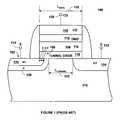
- FIG. 1illustrates a single conventional flash EEPROM memory cell having a double-diffused source region.
- flash memory cell 100is formed on a p-type substrate 110 and includes an n type double-diffused source region 102 and an n+ drain region 104 .
- the drain region 104 and the source region 102are spaced apart from each other forming a channel region 122 .
- a source electrode 114 and a drain electrode 112are connected to the source region 102 and the drain region 104 , respectively.
- the double-diffused source region 102is formed of a lightly doped n region 128 (phosphorous doped) and a more heavily doped but shallower n+ region 130 (arsenic doped) embedded within the deep n region 128 .
- the phosphorus doping within n region 128reduces the horizontal electric field between the source region 102 and the substrate 110 .
- the floating gate 106is disposed a short distance above the source region 102 , the drain region 104 and the channel region 122 over a dielectric layer 118 , which is also known as a tunnel oxide region.
- a control gate 108Above the floating gate 106 and disposed over the dielectric layer 116 is a control gate 108 .
- the dielectric layer 116is typically formed of an oxide/nitride/oxide layer known in the semiconductor manufacturing art as an ONO layer.
- a control gate electrode 120is attached to control gate 108 .
- the dimension L GATE 132represents the gate length for the gates contained in flash memory cell 100 .
- the programming of a flash EEPROM memory cellis achieved by inducing “hot electron” injection from a section of the channel 122 near the drain 104 into the floating gate 106 .
- the injected electronscause the floating gate 106 to carry a negative charge.
- Grounding the source region 102 , biasing the control gate 108 to a relatively high positive voltage and biasing the drain region 104 to a moderate positive voltageinduce the hot electrons.
- the source electrode 114is connected to ground, the drain electrode 112 is connected to a relatively high voltage (typically +4 volts to +9 volts) and the control gate electrode 120 is connected to a relatively high voltage level (typically +8 volts to +12 volts). Electrons are accelerated from source region 102 to drain region 104 via the channel 122 and the “hot electrons” are generated near the drain region 104 . Some of the hot electrons are injected through he relatively thin gate dielectric layer 118 and become trapped in the floating gate 106 thereby giving floating gate 106 a negative potential.
- the negative potential of floating gate 106raises the threshold voltage of the stacked gate transistor and inhibits current flow through the channel 122 during a subsequent “read” mode.
- the magnitude of the read currentis used to determine whether a memory cell has been programmed.
- electronsare typically driven out of the floating gate 106 by biasing the control gate 108 to a large negative voltage and biasing the source region 102 to a low positive voltage in order to produce a sufficiently large vertical electric field in the tunnel oxide.
- the large vertical field 136 in the tunnel oxideproduces Fowler-Nordheim (F-N) tunneling of electrons stored in the floating gate 106 through the tunnel oxide into the source region 102 .
- Arrows 105indicate the tunneling of the electrons from the floating gate 106 to the source region 102 .
- the charge removed from the floating gate 106produces a threshold voltage shift.
- a relatively low positive voltagetypically from +0.5 volts to +5 volts
- a relatively large negative voltagetypically from ⁇ 7 volts to ⁇ 13 volts
- the voltage of the substrate electrode 126is grounded and the drain electrode 112 is allowed to float.
- the vertical electric filed established between the control gate 108 and the source region 102induces electrons previously stored in floating gate 106 to pass through dielectric layer 118 and into source region 102 by way of Fowler-Nordheim tunneling.
- V FG⁇ CG ( V CG ⁇ V T )+ ⁇ S V S + ⁇ B V B
- V FGthe floating gate voltage
- V CGthe control gate voltage
- V Sthe source voltage
- V Bthe substrate or p-well bias
- ⁇ V Tthe threshold voltage difference arising from negative charge added to the floating gate as measured from the control gate
- ⁇ CGthe capacitive coupling coefficient from the control gate to the floating gate
- ⁇ Sthe capacitive coupling coefficient between the source and the floating gate
- ⁇ Bthe capacitive coupling coefficient between the substrate or p-well and the floating gate.
- the memory cellsare typically scaled down in size, for example the reduction in overall footprint of the device, is accomplished by reducing the gate length (L GATE ) 132 .
- L GATEgate length
- a problem with reducing the length of the memory cell gatesis that the distance L CHHANNEL 122 between the source region 102 and the drain region 104 must also be reduced.
- the lateral diffusion of the phosphorous in the source region 128causes a leakage between the source region 102 and the drain region 104 resulting in detrimental short channel effects. Short channel effects produce serious problems in the flash memory cells and are typically evident when the gate length (L GATE ) 132 is reduced below 0.4 microns.
- One method for reducing the short-channel effectwould be to eliminate the double-diffused phosphorous region 128 .
- the phosphorous diffusion overlap distance L DD 124would no longer present and the short channel effect problem would be significantly reduced. Eliminating the phosphorous diffusion overlap distance L DD 124 would allow for a gate length (L GATE ) reduction below 0.4 microns and would provide for an increased packing density of the memory cells.
- J b-t-bA b-t-b ⁇ ( E )e ⁇ (B b-t-b /E)
- J b-t-bband-to-band current density (amps/cm 2 )
- ESQRT (E V 2 +E H 2 ) (the tunneling field in the junction).
- band-to-band currentsalso known as Zener currents
- the band-to-band currentsare normally several orders of magnitude larger than the Fowler-Nordheim current. This band-to-band current is hard to sustain from a circuit design point of view and is also believed to generate detrimental reliability problems such as hole trapping in the tunnel oxide.
- One barrier to further decrease the size of flash memory cellsis that during manufacture of the flash memory cells, there is a phenomenon called gate-edge lifting that occurs during oxidation procedures. Gate edge lifting causes the tunnel oxide to thicken at each end and is a particular problem at the source end of the tunnel oxide through which the electrons must tunnel during Fowler-Nordheim erasure. Because the gate edge lifting is not the same for each memory cell, the erase characteristics of each memory cell may differ and as a result the erase procedure has to be extended to ensure that all memory cells are erased. In addition, in order for each memory cell to be erased at the lowest possible voltage the source region has to be extended under the gate region until the heavily doped region of the double diffused source region reaches a region under the tunnel oxide that has not been thickened. This ensures that the erase characteristics for all the memory cells are the same. However, the extension of the source region under the gate until the heavily doped region reaches a non-thickened portion under the tunnel region prevents the memory cell from being shortened.
- a gate stackis formed on a substrate wherein the gate stack comprises a layer of tunnel oxide, a floating gate, a layer of ONO and a control gate. Portions of the tunnel oxide are etched forming cavities underneath each end of the floating gate thus exposing corners of each end of the floating gate. In the same process, the corners of the floating gate are oxidized and etched thus blunting the comers of the floating gate.
- a layer of oxideis anisotropically deposited on the surfaces of the gate stack that fill the cavities.
- the layer of oxideis etched to form spacers on the side of the gate stack.
- a double diffused source region and a drain regionare formed in the substrate.
- the described method of manufacturing a flash memory cellthus provides a flash memory cell having blunted corners on the floating gate thus allowing less required gate edge lifting.
- FIG. 1shows the structure of a typical flash memory cell
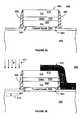
- FIGS. 2A-2Dillustrate a portion of a prior art process for the manufacture of flash memory devices
- FIG. 2Ashows a portion of a flash memory device including a substrate, a layer of tunnel oxide formed on the substrate and a “gate stack” formed on the layer of tunnel oxide comprising a floating gate, a layer of ONO and a control gate;
- FIG. 2Bshows the portion of the flash memory device as shown in FIG. 2A after an oxidation process to form a thin layer of oxide on the gate stack to protect the gate stack from a subsequent ion implantation process;
- FIG. 2Cshows the portion of the flash memory device as shown in FIG. 2B undergoing an ion implantation to form source and drain regions;
- FIG. 2Dshows the portion of the flash memory device as shown in FIG. 2C after an anneal process to drive the implanted ions into the substrate to form the source and drain regions;
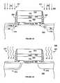
- FIG. 2Eshows the Fowler-Nordheim tunneling paths of electrons during erase in a memory cell with no gate edge lifting
- FIG. 2Fshows the Fowler-Nordheim tunneling paths of electrons during erase in a memory cell with gate edge lifting
- FIGS. 3A-3Gillustrate a portion of a process for the manufacture of flash memory devices in accordance with the present invention
- FIG. 3Ashows a portion of a flash memory device including a substrate, a layer of tunnel oxide formed on the substrate and a “gate stack” formed on the layer of tunnel oxide comprising a floating gate, a layer of ONO and a control gate;
- FIG. 3Bshows the portion of the flash memory device as shown in FIG. 3A after a hydrogen fluoride cleaning/oxidizing process that etches a portion of the layer of tunnel oxide under the floating gate forming cavities in the tunnel oxide and blunts the corners of the gate edges;
- FIG. 3Cshows the portion of the flash memory device as shown in FIG. 3B after an oxide has been anisotropically deposited on the flash memory device and etched to form a protective coating on the sides of the gate stack and that fills the cavities formed in the tunnel oxide;
- FIG. 3Dshows the portion of the flash memory device as shown in FIG. 3C with a patterned mask formed on the surface of the flash memory device and being implanted with phosphorus ions that will form the phosphorus implanted region of the double diffused source;
- FIG. 3Eshows the portion of the flash memory device as shown in FIG. 3D being implanted with arsenic ions to form the arsenic implanted region of the double diffused source and the drain region;
- FIG. 3Fshows the portion of the flash memory device as shown in FIG. 3E undergoing an anneal process to drive the implanted ions into the substrate and to repair damage caused by the implantation process.
- FIG. 3Gshows the portion of the flash memory device as shown in FIG. 3F undergoing an anneal procedure.
- FIGS. 2A-2Dillustrate a portion of a prior art process for the manufacture of flash memory devices.
- FIG. 2Ashows a portion 200 of a flash memory cell that includes a substrate 202 with a layer 204 of tunnel oxide formed on the surface of the substrate 202 .
- a structure 206 known as a gate stackis formed on the layer 204 of tunnel oxide.
- the gate stack 206 structureis formed by forming a layer of polysilicon that will be the floating gate 208 , layer 210 of ONO, which is a thin layer of silicon oxide, a thin layer of silicon nitride, and a thin layer of silicon oxide, and a layer of polysilicon that will be the control gate 212 .
- an etch processforms the gate stack as shown in FIG. 2 A.
- FIG. 2Bshows the portion 200 of the flash memory device as shown in FIG. 2A after an oxidation process that serves to form a protective layer 214 of oxide on the gate stack to specifically protect the exposed ends of the polysilicon material that will form the floating gate 208 and the control gate 212 by forming the thin layer of oxide 214 that forms on exposed silicon surfaces.
- the oxidation processcauses gate edge lifting as shown at 216 and causes oxide to form underneath a portion of the layer 204 of tunnel oxide as indicated at 218 .
- the substratewhich is formed from lightly doped silicon, will oxidize as shown by the solid lines 220 and 222 .
- the dashed lines 224show the original outline of the silicon substrate 202 .
- the dashed lines 226show the original outline of the tunnel oxide 204 .
- FIG. 2Cshows the portion 200 of the flash memory device as shown in FIG. 2B with arrows 228 representing various ion implantations into the substrate 202 that will form the double diffused source region and the drain region.
- arrows 228representing various ion implantations into the substrate 202 that will form the double diffused source region and the drain region.
- FIG. 2Dshows the portion 200 of the flash memory device as shown in FIG. 2C after an anneal process to drive the phosphorus and arsenic ions into the substrate 202 to form the phosphorus implanted source region 230 and the arsenic implanted source region 232 .
- the anneal processcauses further oxidation, which causes the layer of oxide to increase in thickness.
- the anneal processis an oxidizing process in order to repair the damage done during the implantation of dopant ions. This oxidation causes increased gate edge lifting because the oxidation is enhanced by the high impurity concentration of dopants from the implantations.
- the dashed line 238indicates the original thickness of the oxide layer 214 resulting from the first oxidation and the line 240 indicates the outline of the increased thickness of the layer of oxide.
- the anneal processalso causes increased gate edge lifting as indicated at 242 .
- phosphorus ionsmigrate more readily than arsenic ions and a single anneal in a region that contain both phosphorus ions and arsenic ions can result in a double diffused region as shown by regions 230 and 232 .
- the tunnel oxide at the source endhas been thickened in the region at which the electrons indicated at 236 must tunnel from the floating gate 204 to the source region 232 across the tunnel oxide 204 during the Fowler-Nordheim erase procedure.
- the electronstunnel across the tunnel oxide 204 to the portion of the double diffused source region that has arsenic ions implanted.
- the electronshave to tunnel through a thicker tunnel oxide, which as also discussed above, may vary from memory cell to memory cell and may cause each memory cell to have differing erase characteristics.
- the phosphorus implanted region of the double diffused source regionmust be driven further under the tunnel oxide and to maintain the minimum required channel length the size of the memory cell cannot be decreased. Therefore, it should be obvious that a process that does not include the second anneal/oxidation process would allow shorter memory cells and less gate edge lifting.
- FIG. 2Eillustrates the path taken by electrons during a Fowler-Nordheim erase in a memory cell with no gate edge lifting.
- the regions 230 and 232are the phosphorus and arsenic doped regions of the double diffused source.
- the boundary line 250denotes the extent of the phosphorus-doped region.
- the boundary line 252denotes the extent of the arsenic-doped region and the lines 254 , 256 and 258 denote increasing concentration profiles in the arsenic-doped region. Without gate edge lifting the thickness of the tunnel oxide 204 is the same in the region of the arsenic doped region 232 .
- the electronstend to tunnel from the floating gate 208 to the highest concentration regions of the arsenic doped region 232 . This tendency is indicated by the thick dashed arrow 260 , the medium dashed arrow 262 , and the thin dashed arrow 264 .
- the tunnelingfalls off exponentially in the direction of the arrow 266 .
- the problem with the majority of the tunneling occurring from the corner 267is that the tunnel oxide in that region becomes stressed and can cause early failure of the device.
- FIG. 2Fshows the Fowler-Nordheim tunneling paths of electrons during erase in a memory cell with gate edge lifting.
- the gate edge liftingis indicated at 242 both above and below the tunnel oxide 204 .
- the arrow 266indicates the falling off exponentially of electron tunneling as described above in FIG. 2 E.
- the arrow 268indicates the falling off exponentially of electron tunneling as the thickness increases.
- FIGS. 3A-3Gillustrate a portion of a process for the manufacture of flash memory devices in accordance with the present invention.
- FIG. 3Ashows a portion 300 of a flash memory device that includes a substrate 302 with a layer 304 of tunnel oxide formed on the surface of the substrate 302 .
- a structure 306 known as a gate stackis formed on the layer 304 of tunnel oxide.
- the gate stack 306 structureis formed by forming a layer of polysilicon that will be the floating gate 308 , layer 310 of ONO, which is a thin layer of silicon oxide, a thin layer of silicon nitride, and a thin layer of silicon oxide, and a layer of polysilicon that will be the control gate 312 .
- an etch processforms the gate stack as shown in FIG. 3 A.
- FIG. 3Bshows the portion 300 of the flash memory device as shown in FIG. 3A after a process that removes portions of the layer 304 forming cavities 301 in the tunnel oxide underneath the floating gate 308 .
- the process that forms the cavities 301 in the tunnel oxidecan be a process such as a hydrogen fluoride cleaning process or other isotropic etch process suitable for etching oxide.
- a weak oxidizing agentis added to the cleaning agent that oxidizes the surface of the floating gate 308 , which is then attacked by the cleaning agent.
- the combined oxidizing/etching processcauses the corner 309 of the floating gate 308 to be “blunted” or rounded.
- the portion of the flash memory device within dashed circle 311is shown enlarged in FIG. 3 C.
- FIG. 3Cshows the corner 309 of the floating gate 308 , the cavity 301 and the shape 313 of the corner 309 after the combined oxidizing/etching process.
- FIG. 3Dshows the portion 300 of the flash memory device as shown in FIG. 3B after a process of isotropically depositing oxide on the flash memory device and anisotropically etching the oxide to form spacers 305 and 307 as shown in FIG. 3 D.
- FIG. 3Eshows the portion 300 of the flash memory device as shown in FIG. 3D being implanted with phosphorus (P) ions as indicated by arrows 311 .
- a patterned mask layer 313protects portions of the flash memory device that are not to receive phosphorus ions.
- the phosphorus ionsare to form the phosphorus implanted region of the double diffused source region of the device.
- the phosphorus ionsare implanted beneath the surface of the substrate 302 and initially are concentrated generally in a region indicated by the dashed shape 315 . It is noted that the spacer 305 protects the ends of the control gate 312 and floating gate 308 from damage that would be caused by the implantation of the phosphorus ions.
- FIG. 3Fshows the portion 300 of the flash memory device as shown in FIG. 3E with the mask layer 313 removed and being implanted with arsenic ions (As) as indicated by arrows 317 .
- the arsenic ionsare to form the arsenic implanted region of the double diffused source region and to form the drain region of the flash memory device.
- the arsenic ionsare implanted beneath the surface of the substrate 302 and initially are concentrated generally in regions indicated by the dashed shapes 319 . It is noted that the spacers 305 and 307 protects the ends of the control gate 312 and floating gate 308 from damage that would be caused by the implantation of the arsenic ions.
- FIG. 3Gshows the portion 300 of the flash memory device as shown in FIG. 3F undergoing an anneal procedure, indicated by the wavy arrows 321 , the purpose of which is to drive the implanted arsenic ions and phosphorus ions into the substrate 302 to form the double diffused source region 323 and the drain region 325 .
- the anneal procedurealso repairs damage to the substrate caused by the implantation procedure.
- the present inventionovercomes the limitations of the prior art and fulfills the need for a flash memory cell that provides blunted corners on the floating gate thus allowing less required gate edge lifting.
Landscapes
- Non-Volatile Memory (AREA)
Abstract
Description
Claims (5)
Priority Applications (1)
| Application Number | Priority Date | Filing Date | Title |
|---|---|---|---|
| US09/476,584US6238978B1 (en) | 1999-11-05 | 2000-01-03 | Use of etch to blunt gate corners |
Applications Claiming Priority (2)
| Application Number | Priority Date | Filing Date | Title |
|---|---|---|---|
| US16376199P | 1999-11-05 | 1999-11-05 | |
| US09/476,584US6238978B1 (en) | 1999-11-05 | 2000-01-03 | Use of etch to blunt gate corners |
Publications (1)
| Publication Number | Publication Date |
|---|---|
| US6238978B1true US6238978B1 (en) | 2001-05-29 |
Family
ID=26859922
Family Applications (1)
| Application Number | Title | Priority Date | Filing Date |
|---|---|---|---|
| US09/476,584Expired - LifetimeUS6238978B1 (en) | 1999-11-05 | 2000-01-03 | Use of etch to blunt gate corners |
Country Status (1)
| Country | Link |
|---|---|
| US (1) | US6238978B1 (en) |
Cited By (29)
| Publication number | Priority date | Publication date | Assignee | Title |
|---|---|---|---|---|
| US20020123180A1 (en)* | 2001-03-01 | 2002-09-05 | Peter Rabkin | Transistor and memory cell with ultra-short gate feature and method of fabricating the same |
| US6509612B2 (en)* | 2001-05-04 | 2003-01-21 | International Business Machines Corporation | High dielectric constant materials as gate dielectrics (insulators) |
| US6627498B2 (en)* | 2002-02-07 | 2003-09-30 | Infineon Technologies Ag | Memory cell fabrication method and memory cell configuration |
| US20050087819A1 (en)* | 2003-10-28 | 2005-04-28 | Fujitsu Limited | Semiconductor device and manufacturing method thereof |
| US20050119938A1 (en)* | 2003-11-17 | 2005-06-02 | Smith Richard T. | Method for providing consumer benefits using a club program |
| US20060019436A1 (en)* | 2004-07-21 | 2006-01-26 | Hynix Semiconductor Inc. | Transistor of semiconductor device and method of manufacturing the same |
| US20080061359A1 (en)* | 2006-02-04 | 2008-03-13 | Chungho Lee | Dual charge storage node with undercut gate oxide for deep sub-micron memory cell |
| US20080203542A1 (en)* | 1998-09-03 | 2008-08-28 | Micron Technology, Inc. | Ion-assisted oxidation methods and the resulting structures |
| US20100207188A1 (en)* | 2006-09-26 | 2010-08-19 | Kabushiki Kaisha Toshiba | Semiconductor device and method of fabricating the same |
| WO2012003301A2 (en) | 2010-06-30 | 2012-01-05 | Sandisk Technologies Inc. | Ultrahigh density vertical nand memory device and method of making thereof |
| US8187936B2 (en) | 2010-06-30 | 2012-05-29 | SanDisk Technologies, Inc. | Ultrahigh density vertical NAND memory device and method of making thereof |
| US8193054B2 (en) | 2010-06-30 | 2012-06-05 | SanDisk Technologies, Inc. | Ultrahigh density vertical NAND memory device and method of making thereof |
| US8198672B2 (en) | 2010-06-30 | 2012-06-12 | SanDisk Technologies, Inc. | Ultrahigh density vertical NAND memory device |
| US8349681B2 (en) | 2010-06-30 | 2013-01-08 | Sandisk Technologies Inc. | Ultrahigh density monolithic, three dimensional vertical NAND memory device |
| US8928061B2 (en) | 2010-06-30 | 2015-01-06 | SanDisk Technologies, Inc. | Three dimensional NAND device with silicide containing floating gates |
| US9105736B2 (en) | 2009-03-19 | 2015-08-11 | Samsung Electronics Co., Ltd. | Three-dimensional nonvolatile memory devices including interposed floating gates |
| US9159739B2 (en) | 2010-06-30 | 2015-10-13 | Sandisk Technologies Inc. | Floating gate ultrahigh density vertical NAND flash memory |
| US9524779B2 (en) | 2014-06-24 | 2016-12-20 | Sandisk Technologies Llc | Three dimensional vertical NAND device with floating gates |
| US9553146B2 (en) | 2014-06-05 | 2017-01-24 | Sandisk Technologies Llc | Three dimensional NAND device having a wavy charge storage layer |
| US9552991B2 (en) | 2014-04-30 | 2017-01-24 | Sandisk Technologies Llc | Trench vertical NAND and method of making thereof |
| US9576966B1 (en) | 2015-09-21 | 2017-02-21 | Sandisk Technologies Llc | Cobalt-containing conductive layers for control gate electrodes in a memory structure |
| US9646975B2 (en) | 2015-09-21 | 2017-05-09 | Sandisk Technologies Llc | Lateral stack of cobalt and a cobalt-semiconductor alloy for control gate electrodes in a memory structure |
| US9780182B2 (en) | 2015-02-04 | 2017-10-03 | Sandisk Technologies Llc | Molybdenum-containing conductive layers for control gate electrodes in a memory structure |
| US9806089B2 (en) | 2015-09-21 | 2017-10-31 | Sandisk Technologies Llc | Method of making self-assembling floating gate electrodes for a three-dimensional memory device |
| US9984963B2 (en) | 2015-02-04 | 2018-05-29 | Sandisk Technologies Llc | Cobalt-containing conductive layers for control gate electrodes in a memory structure |
| US10128261B2 (en) | 2010-06-30 | 2018-11-13 | Sandisk Technologies Llc | Cobalt-containing conductive layers for control gate electrodes in a memory structure |
| US10276583B2 (en) | 2015-10-29 | 2019-04-30 | Sandisk Technologies Llc | Three-dimensional memory device containing composite word lines including a metal silicide and an elemental metal and method of making thereof |
| US10622368B2 (en) | 2015-06-24 | 2020-04-14 | Sandisk Technologies Llc | Three-dimensional memory device with semicircular metal-semiconductor alloy floating gate electrodes and methods of making thereof |
| US10741572B2 (en) | 2015-02-04 | 2020-08-11 | Sandisk Technologies Llc | Three-dimensional memory device having multilayer word lines containing selectively grown cobalt or ruthenium and method of making the same |
Citations (5)
| Publication number | Priority date | Publication date | Assignee | Title |
|---|---|---|---|---|
| JPS53979A (en)* | 1976-06-25 | 1978-01-07 | Hitachi Ltd | Preparation of semiconductor device |
| JPS5933873A (en)* | 1982-08-20 | 1984-02-23 | Hitachi Ltd | Method for manufacturing semiconductor devices |
| JPS63302566A (en)* | 1987-06-02 | 1988-12-09 | Sanyo Electric Co Ltd | Manufacture of mos semiconductor device |
| US6015736A (en)* | 1997-12-19 | 2000-01-18 | Advanced Micro Devices, Inc. | Method and system for gate stack reoxidation control |
| US6025240A (en)* | 1997-12-18 | 2000-02-15 | Advanced Micro Devices, Inc. | Method and system for using a spacer to offset implant damage and reduce lateral diffusion in flash memory devices |
- 2000
- 2000-01-03USUS09/476,584patent/US6238978B1/ennot_activeExpired - Lifetime
Patent Citations (5)
| Publication number | Priority date | Publication date | Assignee | Title |
|---|---|---|---|---|
| JPS53979A (en)* | 1976-06-25 | 1978-01-07 | Hitachi Ltd | Preparation of semiconductor device |
| JPS5933873A (en)* | 1982-08-20 | 1984-02-23 | Hitachi Ltd | Method for manufacturing semiconductor devices |
| JPS63302566A (en)* | 1987-06-02 | 1988-12-09 | Sanyo Electric Co Ltd | Manufacture of mos semiconductor device |
| US6025240A (en)* | 1997-12-18 | 2000-02-15 | Advanced Micro Devices, Inc. | Method and system for using a spacer to offset implant damage and reduce lateral diffusion in flash memory devices |
| US6015736A (en)* | 1997-12-19 | 2000-01-18 | Advanced Micro Devices, Inc. | Method and system for gate stack reoxidation control |
Cited By (58)
| Publication number | Priority date | Publication date | Assignee | Title |
|---|---|---|---|---|
| US8790982B2 (en) | 1998-09-03 | 2014-07-29 | Micron Technology, Inc. | Methods for reoxidizing an oxide and for fabricating semiconductor devices |
| US8492851B2 (en)* | 1998-09-03 | 2013-07-23 | Micron Technology, Inc. | Structures including an at least partially reoxidized oxide material |
| US20080203542A1 (en)* | 1998-09-03 | 2008-08-28 | Micron Technology, Inc. | Ion-assisted oxidation methods and the resulting structures |
| US20020123180A1 (en)* | 2001-03-01 | 2002-09-05 | Peter Rabkin | Transistor and memory cell with ultra-short gate feature and method of fabricating the same |
| US8288219B2 (en) | 2001-03-01 | 2012-10-16 | Hynix Semiconductor, Inc. | Method of forming a non-volatile memory cell using off-set spacers |
| US20080166844A1 (en)* | 2001-03-01 | 2008-07-10 | Hynix Semiconductor, Inc. | Method of Forming a Non-volatile Memory Cell Using Off-set Spacers |
| US8946003B2 (en) | 2001-03-01 | 2015-02-03 | SK Hynix Inc. | Method of forming transistors with ultra-short gate feature |
| US20070148873A1 (en)* | 2001-03-01 | 2007-06-28 | Hynix Semiconductor, Inc. | Method of Forming Transistors with Ultra-short Gate Feature |
| US6509612B2 (en)* | 2001-05-04 | 2003-01-21 | International Business Machines Corporation | High dielectric constant materials as gate dielectrics (insulators) |
| US6627498B2 (en)* | 2002-02-07 | 2003-09-30 | Infineon Technologies Ag | Memory cell fabrication method and memory cell configuration |
| US7235470B2 (en)* | 2003-10-28 | 2007-06-26 | Fujitsu Limited | Semiconductor device and manufacturing method thereof |
| US20050087819A1 (en)* | 2003-10-28 | 2005-04-28 | Fujitsu Limited | Semiconductor device and manufacturing method thereof |
| US20050119938A1 (en)* | 2003-11-17 | 2005-06-02 | Smith Richard T. | Method for providing consumer benefits using a club program |
| US20070114595A1 (en)* | 2004-07-21 | 2007-05-24 | Hynix Semiconductor Inc. | Transistor of a semiconductor device |
| US7189618B2 (en)* | 2004-07-21 | 2007-03-13 | Hynix Semiconductor Inc. | Method of manufacturing a transistor of a semiconductor device |
| US7564090B2 (en) | 2004-07-21 | 2009-07-21 | Hynix Semiconductor Inc. | Transistor of a semiconductor device |
| US20060019436A1 (en)* | 2004-07-21 | 2006-01-26 | Hynix Semiconductor Inc. | Transistor of semiconductor device and method of manufacturing the same |
| US20080061359A1 (en)* | 2006-02-04 | 2008-03-13 | Chungho Lee | Dual charge storage node with undercut gate oxide for deep sub-micron memory cell |
| US20100207188A1 (en)* | 2006-09-26 | 2010-08-19 | Kabushiki Kaisha Toshiba | Semiconductor device and method of fabricating the same |
| US9105736B2 (en) | 2009-03-19 | 2015-08-11 | Samsung Electronics Co., Ltd. | Three-dimensional nonvolatile memory devices including interposed floating gates |
| US9190533B2 (en) | 2009-03-19 | 2015-11-17 | Samsung Electronics Co., Ltd. | Three-dimensional nonvolatile memory devices including interposed floating gates |
| US9337351B2 (en) | 2009-03-19 | 2016-05-10 | Samsung Electronics Co., Ltd. | Three-dimensional nonvolatile memory devices including interposed floating gates |
| US10037888B2 (en) | 2009-03-19 | 2018-07-31 | Samsung Electronics Co., Ltd. | Three-dimensional nonvolatile memory devices including interposed floating gates |
| US8461000B2 (en) | 2010-06-30 | 2013-06-11 | Sandisk Technologies Inc. | Method of making ultrahigh density vertical NAND memory device |
| US8187936B2 (en) | 2010-06-30 | 2012-05-29 | SanDisk Technologies, Inc. | Ultrahigh density vertical NAND memory device and method of making thereof |
| US8450791B2 (en) | 2010-06-30 | 2013-05-28 | Sandisk Technologies Inc. | Ultrahigh density vertical NAND memory device |
| US8461641B2 (en) | 2010-06-30 | 2013-06-11 | Sandisk Technologies Inc. | Ultrahigh density vertical NAND memory device and method of making thereof |
| US8349681B2 (en) | 2010-06-30 | 2013-01-08 | Sandisk Technologies Inc. | Ultrahigh density monolithic, three dimensional vertical NAND memory device |
| US8330208B2 (en) | 2010-06-30 | 2012-12-11 | Sandisk Technologies Inc. | Ultrahigh density monolithic three dimensional vertical NAND string memory device and method of making thereof |
| US8580639B2 (en) | 2010-06-30 | 2013-11-12 | Sandisk Technologies Inc. | Method of making ultrahigh density vertical NAND memory device |
| US8765543B2 (en) | 2010-06-30 | 2014-07-01 | SanDisk Technologies, Inc. | Method of making an ultrahigh density vertical NAND memory device with shielding wings |
| US8283228B2 (en) | 2010-06-30 | 2012-10-09 | Sandisk Technologies Inc. | Method of making ultrahigh density vertical NAND memory device |
| US8829591B2 (en) | 2010-06-30 | 2014-09-09 | Sandisk Technologies Inc. | Ultrahigh density vertical NAND memory device |
| US8928061B2 (en) | 2010-06-30 | 2015-01-06 | SanDisk Technologies, Inc. | Three dimensional NAND device with silicide containing floating gates |
| US8946810B2 (en) | 2010-06-30 | 2015-02-03 | Sandisk Technologies Inc. | Ultrahigh density vertical NAND memory device |
| US8198672B2 (en) | 2010-06-30 | 2012-06-12 | SanDisk Technologies, Inc. | Ultrahigh density vertical NAND memory device |
| US8193054B2 (en) | 2010-06-30 | 2012-06-05 | SanDisk Technologies, Inc. | Ultrahigh density vertical NAND memory device and method of making thereof |
| CN102959693B (en)* | 2010-06-30 | 2015-08-19 | 桑迪士克科技股份有限公司 | Ultra-high density vertical and non-memory device and method of manufacturing the same |
| US9159739B2 (en) | 2010-06-30 | 2015-10-13 | Sandisk Technologies Inc. | Floating gate ultrahigh density vertical NAND flash memory |
| US9165940B2 (en) | 2010-06-30 | 2015-10-20 | Sandisk Technologies Inc. | Three dimensional NAND device with silicide containing floating gates and method of making thereof |
| CN102959693A (en)* | 2010-06-30 | 2013-03-06 | 桑迪士克科技股份有限公司 | Ultra-high density vertical and non-memory device and method of manufacturing the same |
| US9230976B2 (en) | 2010-06-30 | 2016-01-05 | Sandisk Technologies Inc. | Method of making ultrahigh density vertical NAND memory device |
| WO2012003301A3 (en)* | 2010-06-30 | 2012-04-19 | Sandisk Technologies Inc. | Ultrahigh density vertical nand memory device and method of making thereof |
| US9484358B2 (en) | 2010-06-30 | 2016-11-01 | Sandisk Technologies Llc | Ultrahigh density vertical NAND memory device and method of making thereof |
| US10128261B2 (en) | 2010-06-30 | 2018-11-13 | Sandisk Technologies Llc | Cobalt-containing conductive layers for control gate electrodes in a memory structure |
| WO2012003301A2 (en) | 2010-06-30 | 2012-01-05 | Sandisk Technologies Inc. | Ultrahigh density vertical nand memory device and method of making thereof |
| US9831268B2 (en) | 2010-06-30 | 2017-11-28 | Sandisk Technologies Llc | Ultrahigh density vertical NAND memory device and method of making thereof |
| US9552991B2 (en) | 2014-04-30 | 2017-01-24 | Sandisk Technologies Llc | Trench vertical NAND and method of making thereof |
| US9553146B2 (en) | 2014-06-05 | 2017-01-24 | Sandisk Technologies Llc | Three dimensional NAND device having a wavy charge storage layer |
| US9524779B2 (en) | 2014-06-24 | 2016-12-20 | Sandisk Technologies Llc | Three dimensional vertical NAND device with floating gates |
| US9780182B2 (en) | 2015-02-04 | 2017-10-03 | Sandisk Technologies Llc | Molybdenum-containing conductive layers for control gate electrodes in a memory structure |
| US9984963B2 (en) | 2015-02-04 | 2018-05-29 | Sandisk Technologies Llc | Cobalt-containing conductive layers for control gate electrodes in a memory structure |
| US10741572B2 (en) | 2015-02-04 | 2020-08-11 | Sandisk Technologies Llc | Three-dimensional memory device having multilayer word lines containing selectively grown cobalt or ruthenium and method of making the same |
| US10622368B2 (en) | 2015-06-24 | 2020-04-14 | Sandisk Technologies Llc | Three-dimensional memory device with semicircular metal-semiconductor alloy floating gate electrodes and methods of making thereof |
| US9576966B1 (en) | 2015-09-21 | 2017-02-21 | Sandisk Technologies Llc | Cobalt-containing conductive layers for control gate electrodes in a memory structure |
| US9646975B2 (en) | 2015-09-21 | 2017-05-09 | Sandisk Technologies Llc | Lateral stack of cobalt and a cobalt-semiconductor alloy for control gate electrodes in a memory structure |
| US9806089B2 (en) | 2015-09-21 | 2017-10-31 | Sandisk Technologies Llc | Method of making self-assembling floating gate electrodes for a three-dimensional memory device |
| US10276583B2 (en) | 2015-10-29 | 2019-04-30 | Sandisk Technologies Llc | Three-dimensional memory device containing composite word lines including a metal silicide and an elemental metal and method of making thereof |
Similar Documents
| Publication | Publication Date | Title |
|---|---|---|
| US6238978B1 (en) | Use of etch to blunt gate corners | |
| US6255165B1 (en) | Nitride plug to reduce gate edge lifting | |
| US5652447A (en) | Flash EEPROM memory with reduced column leakage current | |
| US6885590B1 (en) | Memory device having A P+ gate and thin bottom oxide and method of erasing same | |
| US6744675B1 (en) | Program algorithm including soft erase for SONOS memory device | |
| US6287917B1 (en) | Process for fabricating an MNOS flash memory device | |
| US5574685A (en) | Self-aligned buried channel/junction stacked gate flash memory cell | |
| WO2005048269A2 (en) | Flash memory programming using gate induced junction leakage current | |
| JPH07221209A (en) | Flash EEPROM cell with gap between floating gate and drain for high hot electron injection efficiency for programming | |
| US6294430B1 (en) | Nitridization of the pre-ddi screen oxide | |
| JP4419699B2 (en) | Nonvolatile semiconductor memory device and operation method thereof | |
| US6207978B1 (en) | Flash memory cells having a modulation doped heterojunction structure | |
| US6049479A (en) | Operational approach for the suppression of bi-directional tunnel oxide stress of a flash cell | |
| JP3968107B2 (en) | Method for forming a non-volatile memory structure having a floating gate | |
| US6329273B1 (en) | Solid-source doping for source/drain to eliminate implant damage | |
| US6894932B1 (en) | Dual cell memory device having a top dielectric stack | |
| US6008089A (en) | Method of fabricating a split gate flash memory device | |
| JP2008047726A (en) | Split-gate nonvolatile memory and its manufacturing method | |
| EP0700097B1 (en) | A self-aligned buried channel/junction stacked gate flash memory cell | |
| JP2005525695A (en) | Method for manufacturing a memory cell | |
| US6518072B1 (en) | Deposited screen oxide for reducing gate edge lifting | |
| US6303454B1 (en) | Process for a snap-back flash EEPROM cell | |
| US6862221B1 (en) | Memory device having a thin top dielectric and method of erasing same | |
| US6188101B1 (en) | Flash EPROM cell with reduced short channel effect and method for providing same | |
| US6868014B1 (en) | Memory device with reduced operating voltage having dielectric stack |
Legal Events
| Date | Code | Title | Description |
|---|---|---|---|
| AS | Assignment | Owner name:ADVANCED MICRO DEVICES,, CALIFORNIA Free format text:ASSIGNMENT OF ASSIGNORS INTEREST;ASSIGNOR:HUSTER, CARL ROBERT;REEL/FRAME:010487/0313 Effective date:19991102 | |
| STCF | Information on status: patent grant | Free format text:PATENTED CASE | |
| FPAY | Fee payment | Year of fee payment:4 | |
| AS | Assignment | Owner name:SPANSION INC., CALIFORNIA Free format text:ASSIGNMENT OF ASSIGNORS INTEREST;ASSIGNOR:ADVANCED MICRO DEVICES, INC.;REEL/FRAME:019028/0656 Effective date:20070131 | |
| AS | Assignment | Owner name:SPANSION LLC, CALIFORNIA Free format text:ASSIGNMENT OF ASSIGNORS INTEREST;ASSIGNOR:SPANSION INC.;REEL/FRAME:019069/0094 Effective date:20070131 | |
| FPAY | Fee payment | Year of fee payment:8 | |
| AS | Assignment | Owner name:BARCLAYS BANK PLC,NEW YORK Free format text:SECURITY AGREEMENT;ASSIGNORS:SPANSION LLC;SPANSION INC.;SPANSION TECHNOLOGY INC.;AND OTHERS;REEL/FRAME:024522/0338 Effective date:20100510 Owner name:BARCLAYS BANK PLC, NEW YORK Free format text:SECURITY AGREEMENT;ASSIGNORS:SPANSION LLC;SPANSION INC.;SPANSION TECHNOLOGY INC.;AND OTHERS;REEL/FRAME:024522/0338 Effective date:20100510 | |
| FPAY | Fee payment | Year of fee payment:12 | |
| AS | Assignment | Owner name:SPANSION INC., CALIFORNIA Free format text:RELEASE BY SECURED PARTY;ASSIGNOR:BARCLAYS BANK PLC;REEL/FRAME:035201/0159 Effective date:20150312 Owner name:SPANSION LLC, CALIFORNIA Free format text:RELEASE BY SECURED PARTY;ASSIGNOR:BARCLAYS BANK PLC;REEL/FRAME:035201/0159 Effective date:20150312 Owner name:SPANSION TECHNOLOGY LLC, CALIFORNIA Free format text:RELEASE BY SECURED PARTY;ASSIGNOR:BARCLAYS BANK PLC;REEL/FRAME:035201/0159 Effective date:20150312 | |
| AS | Assignment | Owner name:MORGAN STANLEY SENIOR FUNDING, INC., NEW YORK Free format text:SECURITY INTEREST;ASSIGNORS:CYPRESS SEMICONDUCTOR CORPORATION;SPANSION LLC;REEL/FRAME:035240/0429 Effective date:20150312 | |
| AS | Assignment | Owner name:CYPRESS SEMICONDUCTOR CORPORATION, CALIFORNIA Free format text:ASSIGNMENT OF ASSIGNORS INTEREST;ASSIGNOR:SPANSION, LLC;REEL/FRAME:036030/0001 Effective date:20150601 | |
| AS | Assignment | Owner name:CYPRESS SEMICONDUCTOR CORPORATION, CALIFORNIA Free format text:PARTIAL RELEASE OF SECURITY INTEREST IN PATENTS;ASSIGNOR:MORGAN STANLEY SENIOR FUNDING, INC., AS COLLATERAL AGENT;REEL/FRAME:039708/0001 Effective date:20160811 Owner name:SPANSION LLC, CALIFORNIA Free format text:PARTIAL RELEASE OF SECURITY INTEREST IN PATENTS;ASSIGNOR:MORGAN STANLEY SENIOR FUNDING, INC., AS COLLATERAL AGENT;REEL/FRAME:039708/0001 Effective date:20160811 | |
| AS | Assignment | Owner name:MONTEREY RESEARCH, LLC, CALIFORNIA Free format text:ASSIGNMENT OF ASSIGNORS INTEREST;ASSIGNOR:CYPRESS SEMICONDUCTOR CORPORATION;REEL/FRAME:040911/0238 Effective date:20160811 | |
| AS | Assignment | Owner name:MORGAN STANLEY SENIOR FUNDING, INC., NEW YORK Free format text:CORRECTIVE ASSIGNMENT TO CORRECT THE 8647899 PREVIOUSLY RECORDED ON REEL 035240 FRAME 0429. ASSIGNOR(S) HEREBY CONFIRMS THE SECURITY INTERST;ASSIGNORS:CYPRESS SEMICONDUCTOR CORPORATION;SPANSION LLC;REEL/FRAME:058002/0470 Effective date:20150312 |