US6236593B1 - Method for simultaneously programming plural flash memories having invalid blocks - Google Patents
Method for simultaneously programming plural flash memories having invalid blocksDownload PDFInfo
- Publication number
- US6236593B1 US6236593B1US09/558,561US55856100AUS6236593B1US 6236593 B1US6236593 B1US 6236593B1US 55856100 AUS55856100 AUS 55856100AUS 6236593 B1US6236593 B1US 6236593B1
- Authority
- US
- United States
- Prior art keywords
- blocks
- programming
- memory device
- memory
- status information
- Prior art date
- Legal status (The legal status is an assumption and is not a legal conclusion. Google has not performed a legal analysis and makes no representation as to the accuracy of the status listed.)
- Expired - Lifetime
Links
Images


Classifications
- G—PHYSICS
- G06—COMPUTING OR CALCULATING; COUNTING
- G06F—ELECTRIC DIGITAL DATA PROCESSING
- G06F9/00—Arrangements for program control, e.g. control units
- G06F9/06—Arrangements for program control, e.g. control units using stored programs, i.e. using an internal store of processing equipment to receive or retain programs
- G—PHYSICS
- G11—INFORMATION STORAGE
- G11C—STATIC STORES
- G11C16/00—Erasable programmable read-only memories
- G11C16/02—Erasable programmable read-only memories electrically programmable
- G11C16/06—Auxiliary circuits, e.g. for writing into memory
- G11C16/10—Programming or data input circuits
Definitions
- the present inventionrelates to a method for programming an integrated circuit memory device, and more particularly to a method for performing parallel programming for a plurality of flash memories each of which has at least one invalid block.
- a flash memorycontains a memory cell array which is divided into multiple blocks (or referred to as “a sector”) each of which comprises plural memory cells. In such a flash memory, an erasing operation is performed on a block-by-block basis.
- the flash memorymay contain up to, for example, 20 invalid blocks.
- the invalid blocksare defined as blocks that contain one or more invalid bits (or memory cells).
- the flash memories with one or more invalid blockshave the same quality level and AC and DC characteristics as a flash memory with all valid blocks.
- the invalid blocksdo not affect the performance of valid blocks, because the invalid blocks are isolated from the bit line and the common source line (CSL) by a select transistor.
- All blocks of the flash memoryare erased (e.g. written to hexadecimal value ffh) prior to shipping.
- a flash memory with one or more invalid blockswill be programmed with complementary data, e.g. 00h (hereinafter referred to as “block status information”) within the first page, the second page, or all pages of the one or more invalid blocks. These pages may or may not contain the invalid memory cells.
- the block status informationidentifies a block containing invalid memory cells so that the block may be avoided when the flash memory is programmed.
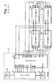
- FIG. 1there is a block diagram showing the structure of a PROM writer system 10 and the flow of signals between the system and plural flash memories 60 .
- An example of the PROM writer systemis described in U.S. Pat. No. 4,783,737, entitled PROM WRITER ADAPTED TO ACCEPT NEW WRITING ALGORITHM, the disclosure of which is hereby incorporated by reference.
- the '737 patentdiscloses a PROM writer system capable of writing data in a PROM via a writing algorithm stored in a memory that is different from the system program memory (so that the algorithm may be changed without change to the system program itself).
- the system 10(hereinafter referred to as “a PROM writer”) is composed of a control unit 20 , e.g. a central processing unit (CPU); a ROM unit 30 for storing a system program and a programming algorithm; a RAM unit 40 for storing data to be programmed in the flash memories 60 a to 60 d ; and an interface unit 50 .
- the control unit 20reads the system program and the programming algorithm stored in the ROM unit 30 and writes the data stored in the RAM unit 40 to the flash memories 60 a to 60 d via the interface unit 50 .
- the data bus for transmitting the data D 0 to Diis shared by the flash memories 60 a to 60 d .
- the address bus for transmitting the address signals A 0 to Aiis shared by the flash memories 60 a to 60 d.
- a read enable signal ⁇ overscore (RE) ⁇ and a write enable signal ⁇ overscore (WE) ⁇ from the PROM writer 10 writerare driven in common to the four flash memories 60 a to 60 d , but the flash memories 60 a , 60 b , 60 c and 60 d are selected independently from each other when corresponding chip select signals ⁇ overscore (CS 0 ) ⁇ , ⁇ overscore (CS 1 ) ⁇ , ⁇ overscore (CS 2 ) ⁇ and ⁇ overscore (CS 3 ) ⁇ are activated, respectively.
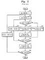
- FIG. 2is a prior art flow chart showing the process of writing the same data in each of the plural flash memories 60 a to 60 d , under the control of the PROM writer 10 illustrated in FIG. 1 .
- FIG. 3shows a memory map of each flash memory illustrated in FIG. 1 .
- the data stored in the RAM unit 40may be written in remaining blocks BLK 3 to BLKn (n: an integer) except for first and second blocks BLK 1 and BLK 2 of each flash memory 60 a to 60 d.
- a first flash memory 60 ais selected by setting a variable DEVICE to ‘1’. That is, a first chip select signal ⁇ overscore (CS 0 ) ⁇ from the PROM writer 10 becomes low (active).
- CS 0chip select signal
- one block BLK 3 of multiple blocks BLK 3 to BLKn of the selected flash memory 60 ais selected by setting a variable BLOCK to ‘3’. Successively, in order to check whether the selected block BLK 3 of the selected flash memory 60 a is valid, block status information is read out from the selected block BLK 3 of the selected flash memory 60 a (step S 13 ).
- the read block status information corresponding to the selected block BLK 3 of the selected flash memory 60 ais stored in the PROM writer 10 , for example, in the RAM unit 40 of the PROM writer 10 (step S 14 ) And then, the data stored in the RAM unit 40 is programmed in the selected block BLK 3 of the selected flash memory 60 a through the interface unit 50 .
- the processproceeds to step S 16 without programming for the selected block BLK 3 after storing the block status information of the selected block BLK 3 . In other words, the programming operation for the selected block BLK 3 is skipped.
- step S 16the control unit 20 of the PROM writer 10 checks whether the selected block BLK 3 is a last block to be programmed. If the selected block BLK 3 is not a last block, the process proceeds to step S 18 , in which the variable BLOCK is increased by one so as to assign a next block. The process from step S 13 to step SI 8 is repeated until a selected block is determined as a last block to be programmed.
- file allocation table (FAT) datain accordance with the block status information, which has been stored temporarily in the RAM unit 40 , is programmed in the first or second block BLK 1 or BLK 2 of the selected flash memory 60 a (step S 19 ).
- file allocation tablemay also be referred to as a “flash file system”.
- flash file systemA suitable flash file system is more fully described in U.S. Pat. No. 5,404,485, entitled FLASH FILE SYSTEM, the disclosure of which is hereby incorporated by reference.
- step S 12 to step S 18is repeated until the remaining flash memories 60 b to 60 d are programmed with the same data as stored in the RAM unit 40 , via the process of steps S 20 and S 21 .
- each of the flash memories 60 a to 60 dis illustrated by the memory map of FIG. 4 .
- the data to be programmed in an invalid blockis stored instead in a next valid block, as indicated by curved arrows.
- the flash memories 60 a to 60 dwhich may have one or more invalid blocks are programmed by means of a serial programming process, thereby increasing the time required for the programming process, according to the prior art.
- a method for programming plural flash memories having one or more invalid blocksEach of the flash memories has a memory cell array which is divided into plural blocks of memory cells. Each of the blocks stores their block status information indicating whether it is valid.
- the programming for the flash memories according to the present inventionis performed under the control of a system, which comprises a control unit, a ROM unit for storing a system program and a program algorithm, a RAM unit for storing program data to be written in the flash memories and an interface unit.
- the block status informationis read out from each memory device, and then is stored in the RAM unit.
- the plural blocks of each memory deviceare divided into first, second and third storage regions in accordance with the stored block status information. Blocks of the second storage regions of the respective memory devices are selected by the system. After selecting memory devices having the selected blocks which are valid, the selected valid blocks of the selected memory devices simultaneously are programmed. If the selected blocks are not the last blocks of the respective second storage regions, a next location of each memory device is designated by the system. The above-described process continues until the selected blocks are determined to be the last blocks of the respective second storage regions.
- the process for programming flash memories having one or more invalid blockscomprises selecting one of the memory devices with at least one invalid block; programming at least one block of the third storage region of the selected memory device instead of the at least one invalid block thereof; programming the stored block status information of the selected memory device in the first storage region of the selected memory device; selecting a next memory device when the selected device is not the last device to be programmed; and continuing to perform the above-described programming process until the selected device is determined to be a last memory device to be programmed.
- a parallel-programming processis performed for valid blocks of all of the flash memories.
- a serial-programming processis performed for flash memories with invalid blocks.
- the time required for programming flash memories with one or more invalid blockscan be reduced by use of the programming algorithm of the present invention.
- FIG. 1is a block diagram showing the structure of a conventional PROM writer system and the flow of signals between the system and flash memories to be programmed;
- FIG. 2is a prior art flow chart showing the process of writing the same data in each of plural flash memories under the control of a system illustrated in FIG. 1;
- FIG. 3shows a memory map of each flash memory illustrated in FIG. 1;
- FIG. 4shows a memory map for each of flash memories when the prior art programming process is finished
- FIG. 6is a memory map for each of flash memories when the programming process of the present invention is finished.
- a programming process of the present inventionwill be performed under the control of a system 10 , e.g. a PROM writer system such as is illustrated in FIG. 1 .
- a system 10e.g. a PROM writer system such as is illustrated in FIG. 1 .
- system 10In order to avoid repetition, further description of system 10 is omitted.
- ROM unit 30 of the system 10there is stored a programming algorithm according to the present invention instead of the programming algorithm according to the prior art.
- the data bus for transmitting the data DO to Diis shared by the flash memories 60 a , 60 b , 60 c and 60 d
- the address bus for transmitting the address signals A 0 to Aiis shared by the flash memories 60 a - 60 d .
- a read enable signal ⁇ overscore (RE) ⁇ and a write enable signal ⁇ overscore (WE) ⁇ from the system 10 of FIG. 1are collectively provided into the flash memories 60 a , 60 b , 60 c and 60 d .
- the flash memories 60 a to 60 dare selected independently from each other when corresponding chip select signals ⁇ overscore (CS 0 ) ⁇ , ⁇ overscore (CS 1 ) ⁇ , ⁇ overscore (CS 2 ) ⁇ and ⁇ overscore (CS 3 ) ⁇ are activated, respectively. They are simultaneously selected when corresponding chip select signals ⁇ overscore (CS 0 ) ⁇ , ⁇ overscore (CS 1 ) ⁇ , ⁇ overscore (CS 2 ) ⁇ and ⁇ overscore (CS 3 ) ⁇ are contemporaneously activated.
- FIG. 5A flow chart showing a programming algorithm of the present invention is illustrated in FIG. 5, which in turn comprises FIGS. 5A and 5B.
- FIGS. 5A and 5BA flow chart showing a programming algorithm of the present invention is illustrated in FIG. 5, which in turn comprises FIGS. 5A and 5B.
- the programming process of the present inventionwill be more fully described with reference to FIGS. 1, 5 and 6 .
- step S 101block status information is read out from all blocks BLK 0 to BLKn of each flash memory 60 a to 60 d , and the block status information is stored in the RAM unit 40 of the system 10 .
- step S 102all of the blocks BLK 0 to BLKn of each flash memory 60 a to 60 d are divided into three storage regions in accordance with the block status information stored in the RAM unit 40 .
- a first storage regionis designated as a portion for storing file allocation table (FAT) information
- a second storage regionas a portion for storing data information to be written in the flash memories 60 a to 60 d (e.g. an application program)
- a third storage regionas the remaining portion.
- a first location of each second storage regionis designated (step S 102 ).
- first and second blocks BLK 1 and BLK 2 of each flash memory 60 a to 60 dare set to the first storage region
- third to mth blocks BLK 3 to BLKm of each flash memory 60 a to 60 dare set to the second storage region
- remaining blocks BLK(m+1) to BLKn (m ⁇ n) of each flash memory 60 a to 60 dare set to the third storage region, as illustrated in FIG. 6 to be more fully explained below.
- the first, second and third storage regions of the respective flash memories 60 a to 60 dare divided so as to have the same number of blocks. It is appreciated by ones skilled in the art that flash memories having different capacity from each other nevertheless may be programmed in accordance with the invention.
- blocks of the second storage regions of the respective memory devices 60 a , 60 b , 60 c and 60 dare selected by sequentially activating chip select signals ⁇ overscore (CS 0 ) ⁇ , ⁇ overscore (CS 1 ) ⁇ , ⁇ overscore (CS 2 ) ⁇ and ⁇ overscore (CS 3 ) ⁇ from the system 10 (step S 103 ).
- the control unit 20 of the system 10checks to see whether the selected blocks BLK 3 of the flash memories 60 a to 60 d are valid, depending on the stored block status information in the RAM unit 40 (step S 104 ).
- the first flash memory 60 ais determined as a device to be programmed. Otherwise, the first flash memory 60 a is designated as a device not to be programmed. The process continues to be performed until it is checked whether the selected blocks BLK 3 of remaining flash memories 60 b to 60 d are valid.
- the selected valid blocks of the selected flash memoriesare simultaneously programmed at step S 104 .
- chip select signals CS 1 and CS 2may be activated which correspond to the flash memories 60 b and 60 c having the selected valid blocks BLK 3 .
- chip select signals ⁇ overscore (CS 0 ) ⁇ and ⁇ overscore (CS 3 ) ⁇ corresponding to the flash memories 60 a and 60 d having invalid blocks BLK 3are inactivated.
- the data stored in the RAM unit 40is simultaneously programmed in the selected blocks BLK 3 of only the second and third flash memories 60 b and 60 c under the control of the system 10 in what is referred to herein as a parallel-programming fashion.
- the invalid blocks BLK 3 of the first and fourth flash memories 60 a and 60 dare prevented from being programmed in accordance with this example via inactivation of their corresponding chip select signals ⁇ overscore (CS 0 ) ⁇ and ⁇ overscore (CS 3 ) ⁇ .
- PROM writer system 10checks whether the selected blocks are the last blocks of the respective second storage regions. So long as the selected blocks are not the last blocks, the process proceeds to step S 106 , in which a next location will be designated. The process from step S 103 to step S 106 is repeated until selected blocks are determined to be the last blocks of the respective second storage regions.
- FIG. 6illustrates a memory map of the contents of the flash memories 60 a to 60 d when the programming process for valid blocks is finished, (see first and second storage regions, so designated).
- blocks BLK 3 of the second storage regions in the first and fourth flash memories 60 a and 60 dare invalid blocks, nevertheless valid blocks BLK 3 of the second and third flash memories 60 b and 60 c are programmed with data DATA 1 at the same time (the parallel-programming). In contrast, no data is written in the invalid blocks BLK 3 corresponding to the first and fourth flash memories 60 a and 60 d .
- blocks BLK 5 of the second storage regions in the second and third flash memories 60 b and 60 care invalid blocks, nevertheless valid blocks BLK 5 corresponding to the first and fourth flash memories 60 a and 60 d are programmed simultaneously with data DATA 3 .
- the system 10selects one of the flash memories 60 a to 60 d with one or more invalid blocks, depending on the block status information stored in the RAM unit 40 .
- Data to be written in the one or more invalid blocksis programmed in blocks of the third storage region of the selected flash memory (step S 108 ). For example, returning to FIG. 6, the data DATAL to be written in the invalid block BLK 3 of the first flash memory 60 a is programmed in (m+1)th block BLK(m+1) of the first flash memory 60 a.
- the stored block status information data in the RAM unit 40is programmed as file allocation table (FAT) data in the first storage region of the selected flash memory (the first flash memory 60 a ).
- FATfile allocation table
- step S 110the system 10 checks whether the selected flash memory is a last flash memory device, having invalid blocks, to be programmed. So long as the selected flash memory is not a last flash memory, the process proceeds to step S 111 , in which a next flash memory will be selected. The process from step S 108 to step S 111 continues to be performed until all the flash memories 60 a to 60 d having one or more invalid blocks have been selected and programmed. In accordance with the immediately above-described serial-programming process, the data corresponding to invalid block(s) of other flash memories 60 b , 60 c and 60 d will be programmed in blocks of corresponding flash memories 60 b to 60 d as shown in FIG. 6 .
- the programming for valid blocks of all the flash memories 60 a to 60 dis performed in parallel.
- the time required for the above-described parallel-programming process for the plural flash memoriesis less than or equal to that required for the process of programming only one flash memory.
- flash memories 60 a to 60 d with one or more invalid blocksare selected and programmed in sequence.
- the time required for programming the plural flash memories with one or more invalid blockscan be significantly reduced by the amount of time saved in programming the more typically valid blocks in parallel while using sequential programming for the less typical invalid blocks.
- flash memory programming timeis reduced.
Landscapes
- Engineering & Computer Science (AREA)
- Software Systems (AREA)
- Theoretical Computer Science (AREA)
- Physics & Mathematics (AREA)
- General Engineering & Computer Science (AREA)
- General Physics & Mathematics (AREA)
- Read Only Memory (AREA)
- Techniques For Improving Reliability Of Storages (AREA)
Abstract
Description
The present invention relates to a method for programming an integrated circuit memory device, and more particularly to a method for performing parallel programming for a plurality of flash memories each of which has at least one invalid block.
As is well known to those skilled in the art, a flash memory contains a memory cell array which is divided into multiple blocks (or referred to as “a sector”) each of which comprises plural memory cells. In such a flash memory, an erasing operation is performed on a block-by-block basis.
The flash memory may contain up to, for example,20 invalid blocks. The invalid blocks are defined as blocks that contain one or more invalid bits (or memory cells). The flash memories with one or more invalid blocks have the same quality level and AC and DC characteristics as a flash memory with all valid blocks. The invalid blocks do not affect the performance of valid blocks, because the invalid blocks are isolated from the bit line and the common source line (CSL) by a select transistor.
All blocks of the flash memory are erased (e.g. written to hexadecimal value ffh) prior to shipping. However, a flash memory with one or more invalid blocks will be programmed with complementary data, e.g. 00h (hereinafter referred to as “block status information”) within the first page, the second page, or all pages of the one or more invalid blocks. These pages may or may not contain the invalid memory cells. The block status information identifies a block containing invalid memory cells so that the block may be avoided when the flash memory is programmed.
Referring to FIG. 1, there is a block diagram showing the structure of aPROM writer system 10 and the flow of signals between the system and plural flash memories60. An example of the PROM writer system is described in U.S. Pat. No. 4,783,737, entitled PROM WRITER ADAPTED TO ACCEPT NEW WRITING ALGORITHM, the disclosure of which is hereby incorporated by reference. The '737 patent discloses a PROM writer system capable of writing data in a PROM via a writing algorithm stored in a memory that is different from the system program memory (so that the algorithm may be changed without change to the system program itself).
The system10 (hereinafter referred to as “a PROM writer”) is composed of acontrol unit 20, e.g. a central processing unit (CPU); aROM unit 30 for storing a system program and a programming algorithm; aRAM unit 40 for storing data to be programmed in theflash memories 60ato60d; and aninterface unit 50. Thecontrol unit 20 reads the system program and the programming algorithm stored in theROM unit 30 and writes the data stored in theRAM unit 40 to theflash memories 60ato60dvia theinterface unit 50. The data bus for transmitting the data D0 to Di is shared by theflash memories 60ato60d. Similarly, the address bus for transmitting the address signals A0 to Ai is shared by theflash memories 60ato60d.
As shown in FIG. 1, a read enable signal {overscore (RE)} and a write enable signal {overscore (WE)} from thePROM writer 10 writer are driven in common to the fourflash memories 60ato60d, but theflash memories
FIG. 2 is a prior art flow chart showing the process of writing the same data in each of theplural flash memories 60ato60d, under the control of thePROM writer 10 illustrated in FIG.1. FIG. 3 shows a memory map of each flash memory illustrated in FIG.1. In FIG. 3, the data stored in theRAM unit 40 may be written in remaining blocks BLK3 to BLKn (n: an integer) except for first and second blocks BLK1 and BLK2 of eachflash memory 60ato60d.
The programming process according to the prior art will be expressed below with reference to the accompanying drawings, with particular reference to FIG.2.
At step S11, afirst flash memory 60ais selected by setting a variable DEVICE to ‘1’. That is, a first chip select signal {overscore (CS0)} from thePROM writer 10 becomes low (active). At step S12, one block BLK3 of multiple blocks BLK3 to BLKn of theselected flash memory 60ais selected by setting a variable BLOCK to ‘3’. Successively, in order to check whether the selected block BLK3 of theselected flash memory 60ais valid, block status information is read out from the selected block BLK3 of theselected flash memory 60a(step S13).
When the selected block BLK3 is determined to be a valid block by means of thecontrol unit 20 of thePROM writer 10, the read block status information corresponding to the selected block BLK3 of theselected flash memory 60ais stored in thePROM writer 10, for example, in theRAM unit 40 of the PROM writer10 (step S14) And then, the data stored in theRAM unit 40 is programmed in the selected block BLK3 of theselected flash memory 60athrough theinterface unit 50. When the selected block BLK3 is determined to be an invalid block by means of thecontrol unit 20, the process proceeds to step S16 without programming for the selected block BLK3 after storing the block status information of the selected block BLK3. In other words, the programming operation for the selected block BLK3 is skipped.
At step S16, thecontrol unit 20 of thePROM writer 10 checks whether the selected block BLK3 is a last block to be programmed. If the selected block BLK3 is not a last block, the process proceeds to step S18, in which the variable BLOCK is increased by one so as to assign a next block. The process from step S13 to stepSI 8 is repeated until a selected block is determined as a last block to be programmed.
When a selected block is discriminated as a last block, file allocation table (FAT) data in accordance with the block status information, which has been stored temporarily in theRAM unit 40, is programmed in the first or second block BLK1 or BLK2 of the selectedflash memory 60a(step S19).
The term “file allocation table” may also be referred to as a “flash file system”. A suitable flash file system is more fully described in U.S. Pat. No. 5,404,485, entitled FLASH FILE SYSTEM, the disclosure of which is hereby incorporated by reference.
The process from step S12 to step S18 is repeated until theremaining flash memories 60bto60dare programmed with the same data as stored in theRAM unit 40, via the process of steps S20 and S21.
When the programming process is finished, the contents of each of theflash memories 60ato60dis illustrated by the memory map of FIG.4. As seen in FIG. 4, the data to be programmed in an invalid block is stored instead in a next valid block, as indicated by curved arrows.
As set forth above, theflash memories 60ato60dwhich may have one or more invalid blocks are programmed by means of a serial programming process, thereby increasing the time required for the programming process, according to the prior art.
It is therefore an object of the present invention to provide a method for simultaneously programming plural flash memories which have at least one invalid block, thereby reducing the programming time on average.
In order to attain the above objects, according to an aspect of the present invention, there is provided a method for programming plural flash memories having one or more invalid blocks. Each of the flash memories has a memory cell array which is divided into plural blocks of memory cells. Each of the blocks stores their block status information indicating whether it is valid. The programming for the flash memories according to the present invention is performed under the control of a system, which comprises a control unit, a ROM unit for storing a system program and a program algorithm, a RAM unit for storing program data to be written in the flash memories and an interface unit.
In the programming algorithm according to the present invention, first, the block status information is read out from each memory device, and then is stored in the RAM unit. The plural blocks of each memory device are divided into first, second and third storage regions in accordance with the stored block status information. Blocks of the second storage regions of the respective memory devices are selected by the system. After selecting memory devices having the selected blocks which are valid, the selected valid blocks of the selected memory devices simultaneously are programmed. If the selected blocks are not the last blocks of the respective second storage regions, a next location of each memory device is designated by the system. The above-described process continues until the selected blocks are determined to be the last blocks of the respective second storage regions.
The process for programming flash memories having one or more invalid blocks comprises selecting one of the memory devices with at least one invalid block; programming at least one block of the third storage region of the selected memory device instead of the at least one invalid block thereof; programming the stored block status information of the selected memory device in the first storage region of the selected memory device; selecting a next memory device when the selected device is not the last device to be programmed; and continuing to perform the above-described programming process until the selected device is determined to be a last memory device to be programmed.
According to the programming method of the present invention, first, a parallel-programming process is performed for valid blocks of all of the flash memories. Then, a serial-programming process is performed for flash memories with invalid blocks. As compared with the prior art which uses only a serial-programming process, the time required for programming flash memories with one or more invalid blocks can be reduced by use of the programming algorithm of the present invention.
The present invention will be described by way of exemplary embodiments, but not limitations, illustrated in the accompanying drawings in which like references denote similar elements, and in which:
FIG. 1 is a block diagram showing the structure of a conventional PROM writer system and the flow of signals between the system and flash memories to be programmed;
FIG. 2 is a prior art flow chart showing the process of writing the same data in each of plural flash memories under the control of a system illustrated in FIG. 1;
FIG. 3 shows a memory map of each flash memory illustrated in FIG. 1;
FIG. 4 shows a memory map for each of flash memories when the prior art programming process is finished;
FIG. 5 including sections5A and5A, is a flow chart showing a programming algorithm according to the present invention; and
FIG. 6 is a memory map for each of flash memories when the programming process of the present invention is finished.
A preferred embodiment of the present invention will be more fully described below with reference to the accompanying drawings. A programming process of the present invention will be performed under the control of asystem 10, e.g. a PROM writer system such as is illustrated in FIG.1. In order to avoid repetition, further description ofsystem 10 is omitted. Importantly, however, in theROM unit 30 of thesystem 10, there is stored a programming algorithm according to the present invention instead of the programming algorithm according to the prior art.
Similarly to the prior art set forth in FIG. 1, the data bus for transmitting the data DO to Di is shared by theflash memories system 10 of FIG. 1 are collectively provided into theflash memories flash memories 60ato60dare selected independently from each other when corresponding chip select signals {overscore (CS0)}, {overscore (CS1)}, {overscore (CS2)} and {overscore (CS3)} are activated, respectively. They are simultaneously selected when corresponding chip select signals {overscore (CS0)}, {overscore (CS1)}, {overscore (CS2)} and {overscore (CS3)} are contemporaneously activated.
A flow chart showing a programming algorithm of the present invention is illustrated in FIG. 5, which in turn comprises FIGS. 5A and 5B. Hereinafter, the programming process of the present invention will be more fully described with reference to FIGS. 1,5 and6.
Referring to FIG. 5A, it may be seen that at step S101, block status information is read out from all blocks BLK0 to BLKn of eachflash memory 60ato60d, and the block status information is stored in theRAM unit 40 of thesystem 10.
At step S102, all of the blocks BLK0 to BLKn of eachflash memory 60ato60dare divided into three storage regions in accordance with the block status information stored in theRAM unit 40. In particular, a first storage region is designated as a portion for storing file allocation table (FAT) information, a second storage region as a portion for storing data information to be written in theflash memories 60ato60d(e.g. an application program), and a third storage region as the remaining portion. A first location of each second storage region is designated (step S102).
For example, first and second blocks BLK1 and BLK2 of eachflash memory 60ato60dare set to the first storage region, third to mth blocks BLK3 to BLKm of eachflash memory 60ato60dare set to the second storage region, and remaining blocks BLK(m+1) to BLKn (m<n) of eachflash memory 60ato60dare set to the third storage region, as illustrated in FIG. 6 to be more fully explained below. As a result, under the condition where theflash memories 60ato60dhave the same memory capacity, the first, second and third storage regions of therespective flash memories 60ato60dare divided so as to have the same number of blocks. It is appreciated by ones skilled in the art that flash memories having different capacity from each other nevertheless may be programmed in accordance with the invention.
And then, to be designated at step S102, blocks of the second storage regions of therespective memory devices control unit 20 of thesystem 10 checks to see whether the selected blocks BLK3 of theflash memories 60ato60dare valid, depending on the stored block status information in the RAM unit40 (step S104).
For example, if the selected block BLK3 of thefirst flash memory 60ais valid, thefirst flash memory 60ais determined as a device to be programmed. Otherwise, thefirst flash memory 60ais designated as a device not to be programmed. The process continues to be performed until it is checked whether the selected blocks BLK3 of remainingflash memories 60bto60dare valid.
After selecting flash memories designated as the device to be programmed at step S104, i.e. flash memories having valid selected blocks BLK3, the selected valid blocks of the selected flash memories are simultaneously programmed at step S104. For example, at step S104, chip select signals CS1 and CS2 may be activated which correspond to theflash memories flash memories RAM unit 40 is simultaneously programmed in the selected blocks BLK3 of only the second andthird flash memories system 10 in what is referred to herein as a parallel-programming fashion. The invalid blocks BLK3 of the first andfourth flash memories
At step S105,PROM writer system 10 checks whether the selected blocks are the last blocks of the respective second storage regions. So long as the selected blocks are not the last blocks, the process proceeds to step S106, in which a next location will be designated. The process from step S103 to step S106 is repeated until selected blocks are determined to be the last blocks of the respective second storage regions. FIG. 6 illustrates a memory map of the contents of theflash memories 60ato60dwhen the programming process for valid blocks is finished, (see first and second storage regions, so designated).
As seen in FIG. 6, although blocks BLK3 of the second storage regions in the first andfourth flash memories third flash memories fourth flash memories third flash memories fourth flash memories third flash memories fourth flash memories 60ato60dare invalid blocks, the blocks BLK4 of theflash memories 60ato60dare nevertheless simultaneously programmed with the same data DATA2.
The process of programming invalid block(s) of each of theflash memories 60ato60dwill be more fully described below with reference to section FIG. 5B of FIG.5.
At step S107, thesystem 10 selects one of theflash memories 60ato60dwith one or more invalid blocks, depending on the block status information stored in theRAM unit 40. Data to be written in the one or more invalid blocks is programmed in blocks of the third storage region of the selected flash memory (step S108). For example, returning to FIG. 6, the data DATAL to be written in the invalid block BLK3 of thefirst flash memory 60ais programmed in (m+1)th block BLK(m+1) of thefirst flash memory 60a.
At step S109, the stored block status information data in theRAM unit 40 is programmed as file allocation table (FAT) data in the first storage region of the selected flash memory (thefirst flash memory 60a).
At step S110, thesystem 10 checks whether the selected flash memory is a last flash memory device, having invalid blocks, to be programmed. So long as the selected flash memory is not a last flash memory, the process proceeds to step S111, in which a next flash memory will be selected. The process from step S108 to step S111 continues to be performed until all theflash memories 60ato60dhaving one or more invalid blocks have been selected and programmed. In accordance with the immediately above-described serial-programming process, the data corresponding to invalid block(s) ofother flash memories flash memories 60bto60das shown in FIG.6.
According to the embodiment of the present invention, first, the programming for valid blocks of all theflash memories 60ato60dis performed in parallel. The time required for the above-described parallel-programming process for the plural flash memories is less than or equal to that required for the process of programming only one flash memory. And then,flash memories 60ato60dwith one or more invalid blocks are selected and programmed in sequence. As a result, the time required for programming the plural flash memories with one or more invalid blocks can be significantly reduced by the amount of time saved in programming the more typically valid blocks in parallel while using sequential programming for the less typical invalid blocks. On average, then, flash memory programming time is reduced.
The invention has been described using exemplary preferred embodiments. However, it is to be understood that the scope of the invention is not limited to the disclosed embodiments. On the contrary, it is intended to cover various modifications and similar arrangements. The scope of the claims, therefore, should be accorded the broadest interpretation so as to encompass all such modifications and similar arrangements.
Claims (8)
1. A method for programming a plurality of electrically programmable nonvolatile memory devices each having a memory cell array divided into plural blocks of memory cells, wherein each of the blocks stores block status information indicating whether it is valid or not, the method comprising the steps of:
(a) reading the block status information from each memory device and storing the block status information in a data storage unit;
(b) dividing the plural blocks of each memory device into first, second and third storage regions in accordance with the stored block status information and designating a first location of each second storage region;
(c) selecting blocks, at the designated location, of the second storage regions of the respective memory devices;
(d) after selecting memory devices having the selected blocks which are valid, simultaneously programming the selected valid blocks of the selected memory devices;
(e) designating a next location of each memory device when the selected blocks are not the last blocks of the respective second storage regions; and
(f) performing the steps (c) through (e) repeatedly until the selected blocks are determined to be the last blocks of the respective second storage regions.
2. The method according to claim1, further comprising the steps of:
(g) selecting one of the memory devices with at least one invalid block;
(h) programming at least one block of the third storage region of the selected memory device instead of the at least one invalid block thereof;
(i) programming the stored block status information of the selected memory device in the first storage region of the selected memory device;
(j) selecting a next memory device when the selected device is not last; and
(k) performing the steps (h) through (j) until the selected device is determined to be a last memory device.
3. The method according to claim1, wherein the data storage unit is a random access memory installed in a system for controlling the programming for plural memory devices.
4. A method for programming electrically programmable nonvolatile memory devices sharing data and address buses, under the control of a system which comprises a central processing unit, an interface unit, a RAM unit, and a ROM unit, wherein each memory device has a memory cell array divided into plural blocks of memory cells, and wherein each of the blocks stores block status information indicating whether it is valid or not, the method comprising the steps of:
(a) reading the block status information from each memory device and storing the block status information in the RAM unit;
(b) dividing the plural blocks of each memory device into first, second and third storage regions in accordance with the stored block status information and designating a first location of each memory device;
(c) selecting blocks, at the designated location, of the second storage regions of the respective memory devices;
(d) after selecting memory devices having the selected blocks which are valid, simultaneously programming the selected valid blocks of the selected memory devices;
(e) checking whether the selected blocks are the last blocks of the respective second storage regions;
(f) designating a next location of each memory device when the selected blocks are not last;
(g) performing the steps (c) through (f) repeatedly until the selected blocks are determined to be the last blocks of the respective second storage regions; and
(h) sequentially programming the memory devices having one or more invalid blocks.
5. The method according to claim4, whererin the step (h) comprises the steps of:
(i) selecting one of the memory devices with at least one invalid block;
(j) programming at least one block of the third storage region of the selected memory device instead of the at least one invalid block thereof;
(k) programming the stored block status information, as the file allocation table data, of the selected memory device in the first storage region of the selected memory device;
(l) selecting a next memory device when the selected device is not last; and
(m) performing the steps (j) through (l) until the selected device is determined to be a last memory device.
6. A method for programming a plurality of flash memory devices each having a memory cell array divided into plural blocks of memory cells, wherein each of the blocks stores block status information indicating whether it is valid or not, the method comprising the steps of:
(a) reading the block status information from each flash memory device and storing the block status information in a data storage unit;
(b) dividing the plural blocks of each flash memory device into first, second and third storage regions in accordance with the stored block status information and designating a first location of each second storage region;
(c) selecting blocks, at the designated location, of the second storage regions of the respective memory devices;
(d) after selecting memory devices having the selected blocks which are valid, simultaneously programming the selected valid blocks of the selected memory devices; and
(e) checking whether the selected blocks are the last blocks of the respective second storage regions;
(f) designating a next location of each memory device when the selected blocks are not last;
(g) performing the steps (c) through (f) repeatedly until the selected blocks are determined to be the last blocks of the respective second storage regions;
(h) selecting one of the memory devices with at least one invalid block;
(i) programming at least one block of the third storage region of the selected memory device instead of the at least one invalid block thereof;
(j) programming the stored block status information of the selected memory device in the first storage region of the selected memory device;
(k) checking whether the selected device is the last device to be programmed;
(l) selecting a next memory device so long as the selected device is not the last device to be programmed; and
(m) performing the steps (i) through (l) until the selected device is determined to be the last memory device to be programmed.
7. The method according to claim6, wherein the memory devices share common data and address buses.
8. The method according to claim6, wherein the method for programming the flash memory devices is performed under the control of a system which comprises a central processing unit, a RAM unit, a ROM unit and an interface unit, wherein the block status information is stored in the RAM unit of the system.
Applications Claiming Priority (2)
| Application Number | Priority Date | Filing Date | Title |
|---|---|---|---|
| KR99-15073 | 1999-04-27 | ||
| KR1019990015073AKR100330164B1 (en) | 1999-04-27 | 1999-04-27 | A method for simultaneously programming plural flash memories having invalid blocks |
Publications (1)
| Publication Number | Publication Date |
|---|---|
| US6236593B1true US6236593B1 (en) | 2001-05-22 |
Family
ID=19582471
Family Applications (1)
| Application Number | Title | Priority Date | Filing Date |
|---|---|---|---|
| US09/558,561Expired - LifetimeUS6236593B1 (en) | 1999-04-27 | 2000-04-26 | Method for simultaneously programming plural flash memories having invalid blocks |
Country Status (3)
| Country | Link |
|---|---|
| US (1) | US6236593B1 (en) |
| JP (1) | JP3842519B2 (en) |
| KR (1) | KR100330164B1 (en) |
Cited By (117)
| Publication number | Priority date | Publication date | Assignee | Title |
|---|---|---|---|---|
| US6570785B1 (en)* | 2000-10-31 | 2003-05-27 | Sandisk Corporation | Method of reducing disturbs in non-volatile memory |
| US6584553B2 (en)* | 2000-07-31 | 2003-06-24 | Exatron, Inc. | Method and system for sequentially programming memory-containing integrated circuits |
| US6587915B1 (en)* | 1999-09-29 | 2003-07-01 | Samsung Electronics Co., Ltd. | Flash memory having data blocks, spare blocks, a map block and a header block and a method for controlling the same |
| US20040027865A1 (en)* | 2000-10-31 | 2004-02-12 | Mangan John S. | Method of reducing disturbs in non-volatile memory |
| US20040103241A1 (en)* | 2002-10-28 | 2004-05-27 | Sandisk Corporation | Method and apparatus for effectively enabling an out of sequence write process within a non-volatile memory system |
| US20040153590A1 (en)* | 2001-06-12 | 2004-08-05 | Andre Roger | Method for programming/parallel programming of onboard flash memory by multiple acces bus |
| US20040186962A1 (en)* | 2003-03-18 | 2004-09-23 | American Megatrends, Inc. | Method, system, and computer-readable medium for updating memory devices in a computer system |
| US20040210729A1 (en)* | 2001-07-23 | 2004-10-21 | Renesas Technology Corp. | Nonvolatile memory |
| US20050188148A1 (en)* | 2004-02-20 | 2005-08-25 | Nec Electronics Corporation | Data access controlling method in flash memory and data access controlling program |
| US20050193233A1 (en)* | 2004-02-03 | 2005-09-01 | Paul Magliocco | Method for testing and programming memory devices and system for same |
| US20060224821A1 (en)* | 2005-04-01 | 2006-10-05 | Mediatek Incorporation | System for parallel updating flash memory and method for the same |
| US7185162B1 (en)* | 2000-10-26 | 2007-02-27 | Cypress Semiconductor Corporation | Method and apparatus for programming a flash memory |
| US20070080436A1 (en)* | 2005-03-22 | 2007-04-12 | Ibm Corporation | System and Method for Noise Reduction in Multi-Layer Ceramic Packages |
| US20070101054A1 (en)* | 2005-09-28 | 2007-05-03 | Muthian Sivathanu | Computer storage device providing implicit detection of block liveness |
| US20080040559A1 (en)* | 2006-08-14 | 2008-02-14 | Barry Joe Wolford | Method and Apparatus to Enable the Cooperative Signaling of a Shared Bus Interrupt in a Multi-Rank Memory Subsystem |
| US20080068883A1 (en)* | 2006-09-15 | 2008-03-20 | Samsung Electronics Co. Ltd. | Flash memory devices and programming methods for the same |
| US20080089138A1 (en)* | 2006-10-11 | 2008-04-17 | Barry Joe Wolford | Concurrent Status Register Read |
| US20080140910A1 (en)* | 2006-12-06 | 2008-06-12 | David Flynn | Apparatus, system, and method for managing data in a storage device with an empty data token directive |
| US20080195854A1 (en)* | 2007-02-13 | 2008-08-14 | Samsung Electronics Company, Ltd. | Electronic Systems Using Flash Memory Modules as Main Storage and Related System Booting Methods |
| US20080263305A1 (en)* | 2007-04-19 | 2008-10-23 | Microsoft Corporation | Remove-on-delete technologies for solid state drive optimization |
| US20090254772A1 (en)* | 2008-04-08 | 2009-10-08 | International Business Machines Corporation | Extending and Scavenging Super-Capacitor Capacity |
| US20090307291A1 (en)* | 2006-03-23 | 2009-12-10 | Beijing Watch Data System Co., Ltd | Smart card storage system and file management method therein |
| US20090327578A1 (en)* | 2008-06-25 | 2009-12-31 | International Business Machines Corporation | Flash Sector Seeding to Reduce Program Times |
| US20090323452A1 (en)* | 2008-06-25 | 2009-12-31 | International Business Machines Corporation | Dual Mode Memory System for Reducing Power Requirements During Memory Backup Transition |
| US20100052625A1 (en)* | 2008-09-04 | 2010-03-04 | International Business Machines Corporation | In Situ Verification of Capacitive Power Support |
| US7737724B2 (en) | 2007-04-17 | 2010-06-15 | Cypress Semiconductor Corporation | Universal digital block interconnection and channel routing |
| US7761845B1 (en) | 2002-09-09 | 2010-07-20 | Cypress Semiconductor Corporation | Method for parameterizing a user module |
| US7765095B1 (en) | 2000-10-26 | 2010-07-27 | Cypress Semiconductor Corporation | Conditional branching in an in-circuit emulation system |
| US7770113B1 (en) | 2001-11-19 | 2010-08-03 | Cypress Semiconductor Corporation | System and method for dynamically generating a configuration datasheet |
| US7774190B1 (en) | 2001-11-19 | 2010-08-10 | Cypress Semiconductor Corporation | Sleep and stall in an in-circuit emulation system |
| US7825688B1 (en) | 2000-10-26 | 2010-11-02 | Cypress Semiconductor Corporation | Programmable microcontroller architecture(mixed analog/digital) |
| US7844437B1 (en) | 2001-11-19 | 2010-11-30 | Cypress Semiconductor Corporation | System and method for performing next placements and pruning of disallowed placements for programming an integrated circuit |
| US7893724B2 (en) | 2004-03-25 | 2011-02-22 | Cypress Semiconductor Corporation | Method and circuit for rapid alignment of signals |
| US20110060887A1 (en)* | 2009-09-09 | 2011-03-10 | Fusion-io, Inc | Apparatus, system, and method for allocating storage |
| US20110066808A1 (en)* | 2009-09-08 | 2011-03-17 | Fusion-Io, Inc. | Apparatus, System, and Method for Caching Data on a Solid-State Storage Device |
| US8026739B2 (en) | 2007-04-17 | 2011-09-27 | Cypress Semiconductor Corporation | System level interconnect with programmable switching |
| US8037380B2 (en) | 2008-07-08 | 2011-10-11 | International Business Machines Corporation | Verifying data integrity of a non-volatile memory system during data caching process |
| US8040266B2 (en) | 2007-04-17 | 2011-10-18 | Cypress Semiconductor Corporation | Programmable sigma-delta analog-to-digital converter |
| US8049569B1 (en) | 2007-09-05 | 2011-11-01 | Cypress Semiconductor Corporation | Circuit and method for improving the accuracy of a crystal-less oscillator having dual-frequency modes |
| US8069428B1 (en) | 2001-10-24 | 2011-11-29 | Cypress Semiconductor Corporation | Techniques for generating microcontroller configuration information |
| US8067948B2 (en) | 2006-03-27 | 2011-11-29 | Cypress Semiconductor Corporation | Input/output multiplexer bus |
| US8069436B2 (en) | 2004-08-13 | 2011-11-29 | Cypress Semiconductor Corporation | Providing hardware independence to automate code generation of processing device firmware |
| US8069405B1 (en) | 2001-11-19 | 2011-11-29 | Cypress Semiconductor Corporation | User interface for efficiently browsing an electronic document using data-driven tabs |
| US8078894B1 (en) | 2007-04-25 | 2011-12-13 | Cypress Semiconductor Corporation | Power management architecture, method and configuration system |
| US8078970B1 (en) | 2001-11-09 | 2011-12-13 | Cypress Semiconductor Corporation | Graphical user interface with user-selectable list-box |
| US8085067B1 (en) | 2005-12-21 | 2011-12-27 | Cypress Semiconductor Corporation | Differential-to-single ended signal converter circuit and method |
| US8085100B2 (en) | 2005-02-04 | 2011-12-27 | Cypress Semiconductor Corporation | Poly-phase frequency synthesis oscillator |
| US8089461B2 (en) | 2005-06-23 | 2012-01-03 | Cypress Semiconductor Corporation | Touch wake for electronic devices |
| US8092083B2 (en) | 2007-04-17 | 2012-01-10 | Cypress Semiconductor Corporation | Temperature sensor with digital bandgap |
| US8103497B1 (en) | 2002-03-28 | 2012-01-24 | Cypress Semiconductor Corporation | External interface for event architecture |
| US8103496B1 (en) | 2000-10-26 | 2012-01-24 | Cypress Semicondutor Corporation | Breakpoint control in an in-circuit emulation system |
| US8120408B1 (en) | 2005-05-05 | 2012-02-21 | Cypress Semiconductor Corporation | Voltage controlled oscillator delay cell and method |
| US8130025B2 (en) | 2007-04-17 | 2012-03-06 | Cypress Semiconductor Corporation | Numerical band gap |
| US8149048B1 (en) | 2000-10-26 | 2012-04-03 | Cypress Semiconductor Corporation | Apparatus and method for programmable power management in a programmable analog circuit block |
| US8160864B1 (en) | 2000-10-26 | 2012-04-17 | Cypress Semiconductor Corporation | In-circuit emulator and pod synchronized boot |
| US8176296B2 (en) | 2000-10-26 | 2012-05-08 | Cypress Semiconductor Corporation | Programmable microcontroller architecture |
| US8286125B2 (en) | 2004-08-13 | 2012-10-09 | Cypress Semiconductor Corporation | Model for a hardware device-independent method of defining embedded firmware for programmable systems |
| US20120317649A1 (en)* | 2010-11-05 | 2012-12-13 | Atc Logistics & Electronics, Inc. | System and method for remotely flashing a wireless device |
| US8402313B1 (en) | 2002-05-01 | 2013-03-19 | Cypress Semiconductor Corporation | Reconfigurable testing system and method |
| US8499270B1 (en) | 2007-04-25 | 2013-07-30 | Cypress Semiconductor Corporation | Configuration of programmable IC design elements |
| US8516025B2 (en) | 2007-04-17 | 2013-08-20 | Cypress Semiconductor Corporation | Clock driven dynamic datapath chaining |
| US8527693B2 (en) | 2010-12-13 | 2013-09-03 | Fusion IO, Inc. | Apparatus, system, and method for auto-commit memory |
| US8527949B1 (en) | 2001-11-19 | 2013-09-03 | Cypress Semiconductor Corporation | Graphical user interface for dynamically reconfiguring a programmable device |
| US8601222B2 (en) | 2010-05-13 | 2013-12-03 | Fusion-Io, Inc. | Apparatus, system, and method for conditional and atomic storage operations |
| TWI420388B (en)* | 2005-11-15 | 2013-12-21 | Samsung Electronics Co Ltd | Method and apparatus for booting a microprocessor system using boot code stored on a serial flash memory array having a random-access interface |
| US8725934B2 (en) | 2011-12-22 | 2014-05-13 | Fusion-Io, Inc. | Methods and appratuses for atomic storage operations |
| US8756375B2 (en) | 2006-12-06 | 2014-06-17 | Fusion-Io, Inc. | Non-volatile cache |
| US8825937B2 (en) | 2011-02-25 | 2014-09-02 | Fusion-Io, Inc. | Writing cached data forward on read |
| US8874823B2 (en) | 2011-02-15 | 2014-10-28 | Intellectual Property Holdings 2 Llc | Systems and methods for managing data input/output operations |
| US8935302B2 (en) | 2006-12-06 | 2015-01-13 | Intelligent Intellectual Property Holdings 2 Llc | Apparatus, system, and method for data block usage information synchronization for a non-volatile storage volume |
| US8966191B2 (en) | 2011-03-18 | 2015-02-24 | Fusion-Io, Inc. | Logical interface for contextual storage |
| US8984216B2 (en) | 2010-09-09 | 2015-03-17 | Fusion-Io, Llc | Apparatus, system, and method for managing lifetime of a storage device |
| US9003104B2 (en) | 2011-02-15 | 2015-04-07 | Intelligent Intellectual Property Holdings 2 Llc | Systems and methods for a file-level cache |
| US9047178B2 (en) | 2010-12-13 | 2015-06-02 | SanDisk Technologies, Inc. | Auto-commit memory synchronization |
| US9058123B2 (en) | 2012-08-31 | 2015-06-16 | Intelligent Intellectual Property Holdings 2 Llc | Systems, methods, and interfaces for adaptive persistence |
| US9116812B2 (en) | 2012-01-27 | 2015-08-25 | Intelligent Intellectual Property Holdings 2 Llc | Systems and methods for a de-duplication cache |
| US9122579B2 (en) | 2010-01-06 | 2015-09-01 | Intelligent Intellectual Property Holdings 2 Llc | Apparatus, system, and method for a storage layer |
| US9201677B2 (en) | 2011-05-23 | 2015-12-01 | Intelligent Intellectual Property Holdings 2 Llc | Managing data input/output operations |
| US9208071B2 (en) | 2010-12-13 | 2015-12-08 | SanDisk Technologies, Inc. | Apparatus, system, and method for accessing memory |
| US9213594B2 (en) | 2011-01-19 | 2015-12-15 | Intelligent Intellectual Property Holdings 2 Llc | Apparatus, system, and method for managing out-of-service conditions |
| US9218278B2 (en) | 2010-12-13 | 2015-12-22 | SanDisk Technologies, Inc. | Auto-commit memory |
| US9223514B2 (en) | 2009-09-09 | 2015-12-29 | SanDisk Technologies, Inc. | Erase suspend/resume for memory |
| US9251086B2 (en) | 2012-01-24 | 2016-02-02 | SanDisk Technologies, Inc. | Apparatus, system, and method for managing a cache |
| US9274937B2 (en) | 2011-12-22 | 2016-03-01 | Longitude Enterprise Flash S.A.R.L. | Systems, methods, and interfaces for vector input/output operations |
| US9305610B2 (en) | 2009-09-09 | 2016-04-05 | SanDisk Technologies, Inc. | Apparatus, system, and method for power reduction management in a storage device |
| US9448964B2 (en) | 2009-05-04 | 2016-09-20 | Cypress Semiconductor Corporation | Autonomous control in a programmable system |
| EP2024840A4 (en)* | 2006-06-08 | 2016-11-23 | Coriant Oy | METHOD AND ARRANGEMENT FOR PROCESSING TRANSACTIONS IN A FLASH TYPE MEMORY DEVICE |
| US9519540B2 (en) | 2007-12-06 | 2016-12-13 | Sandisk Technologies Llc | Apparatus, system, and method for destaging cached data |
| US9564902B2 (en) | 2007-04-17 | 2017-02-07 | Cypress Semiconductor Corporation | Dynamically configurable and re-configurable data path |
| US9563555B2 (en) | 2011-03-18 | 2017-02-07 | Sandisk Technologies Llc | Systems and methods for storage allocation |
| US9600184B2 (en) | 2007-12-06 | 2017-03-21 | Sandisk Technologies Llc | Apparatus, system, and method for coordinating storage requests in a multi-processor/multi-thread environment |
| US9612966B2 (en) | 2012-07-03 | 2017-04-04 | Sandisk Technologies Llc | Systems, methods and apparatus for a virtual machine cache |
| US9640264B2 (en) | 2013-04-01 | 2017-05-02 | Samsung Electronics Co., Ltd. | Memory system responsive to flush command to store data in fast memory and method of operating memory system |
| US9678874B2 (en) | 2011-01-31 | 2017-06-13 | Sandisk Technologies Llc | Apparatus, system, and method for managing eviction of data |
| US9720805B1 (en) | 2007-04-25 | 2017-08-01 | Cypress Semiconductor Corporation | System and method for controlling a target device |
| US9767032B2 (en) | 2012-01-12 | 2017-09-19 | Sandisk Technologies Llc | Systems and methods for cache endurance |
| US9792104B2 (en) | 2010-11-05 | 2017-10-17 | FedEx Supply Chain Logistics & Electronics, Inc. | System and method for flashing a wireless device |
| US9842053B2 (en) | 2013-03-15 | 2017-12-12 | Sandisk Technologies Llc | Systems and methods for persistent cache logging |
| US9842128B2 (en) | 2013-08-01 | 2017-12-12 | Sandisk Technologies Llc | Systems and methods for atomic storage operations |
| US9910777B2 (en) | 2010-07-28 | 2018-03-06 | Sandisk Technologies Llc | Enhanced integrity through atomic writes in cache |
| US9946607B2 (en) | 2015-03-04 | 2018-04-17 | Sandisk Technologies Llc | Systems and methods for storage error management |
| US10009438B2 (en) | 2015-05-20 | 2018-06-26 | Sandisk Technologies Llc | Transaction log acceleration |
| US10019352B2 (en) | 2013-10-18 | 2018-07-10 | Sandisk Technologies Llc | Systems and methods for adaptive reserve storage |
| US10019320B2 (en) | 2013-10-18 | 2018-07-10 | Sandisk Technologies Llc | Systems and methods for distributed atomic storage operations |
| US10068663B1 (en)* | 2017-05-30 | 2018-09-04 | Seagate Technology Llc | Data storage device with rewriteable in-place memory |
| US10073630B2 (en) | 2013-11-08 | 2018-09-11 | Sandisk Technologies Llc | Systems and methods for log coordination |
| TWI637399B (en)* | 2015-01-23 | 2018-10-01 | 慧榮科技股份有限公司 | Memory system and memory-control method with a programming status |
| US10102144B2 (en) | 2013-04-16 | 2018-10-16 | Sandisk Technologies Llc | Systems, methods and interfaces for data virtualization |
| US10133663B2 (en) | 2010-12-17 | 2018-11-20 | Longitude Enterprise Flash S.A.R.L. | Systems and methods for persistent address space management |
| US10133662B2 (en) | 2012-06-29 | 2018-11-20 | Sandisk Technologies Llc | Systems, methods, and interfaces for managing persistent data of atomic storage operations |
| US10318495B2 (en) | 2012-09-24 | 2019-06-11 | Sandisk Technologies Llc | Snapshots for a non-volatile device |
| US10339056B2 (en) | 2012-07-03 | 2019-07-02 | Sandisk Technologies Llc | Systems, methods and apparatus for cache transfers |
| US10509776B2 (en) | 2012-09-24 | 2019-12-17 | Sandisk Technologies Llc | Time sequence data management |
| US10558561B2 (en) | 2013-04-16 | 2020-02-11 | Sandisk Technologies Llc | Systems and methods for storage metadata management |
| US10698662B2 (en) | 2001-11-15 | 2020-06-30 | Cypress Semiconductor Corporation | System providing automatic source code generation for personalization and parameterization of user modules |
| US10817502B2 (en) | 2010-12-13 | 2020-10-27 | Sandisk Technologies Llc | Persistent memory management |
| US10817421B2 (en) | 2010-12-13 | 2020-10-27 | Sandisk Technologies Llc | Persistent data structures |
Families Citing this family (11)
| Publication number | Priority date | Publication date | Assignee | Title |
|---|---|---|---|---|
| JP3822081B2 (en) | 2001-09-28 | 2006-09-13 | 東京エレクトロンデバイス株式会社 | Data writing apparatus, data writing control method, and program |
| KR20030000017A (en)* | 2002-11-29 | 2003-01-03 | (주) 라모스테크놀러지 | Apparatus and Method for controlling flash memories |
| US20050144516A1 (en)* | 2003-12-30 | 2005-06-30 | Gonzalez Carlos J. | Adaptive deterministic grouping of blocks into multi-block units |
| US8122193B2 (en) | 2004-12-21 | 2012-02-21 | Samsung Electronics Co., Ltd. | Storage device and user device including the same |
| KR100684887B1 (en) | 2005-02-04 | 2007-02-20 | 삼성전자주식회사 | Data storage device including flash memory and its merge method |
| KR100703727B1 (en)* | 2005-01-12 | 2007-04-05 | 삼성전자주식회사 | Non-volatile memory, mapping control device and method therefor |
| JP2006223598A (en)* | 2005-02-17 | 2006-08-31 | Daiman:Kk | Game machine |
| JP4859402B2 (en)* | 2005-07-04 | 2012-01-25 | 株式会社アドバンテスト | Test apparatus and manufacturing method |
| KR101336258B1 (en)* | 2007-05-29 | 2013-12-03 | 삼성전자 주식회사 | Apparatus and method of processing data of non-volatile memory |
| JP4720891B2 (en)* | 2008-09-30 | 2011-07-13 | Tdk株式会社 | MEMORY CONTROLLER, FLASH MEMORY SYSTEM HAVING MEMORY CONTROLLER, AND FLASH MEMORY CONTROL METHOD |
| JP5165081B2 (en)* | 2011-05-09 | 2013-03-21 | 株式会社大一商会 | Game machine |
Citations (5)
| Publication number | Priority date | Publication date | Assignee | Title |
|---|---|---|---|---|
| US4783737A (en) | 1985-12-25 | 1988-11-08 | Ando Electric Co., Ltd. | PROM writer adapted to accept new writing algorithm |
| US5404485A (en) | 1993-03-08 | 1995-04-04 | M-Systems Flash Disk Pioneers Ltd. | Flash file system |
| US5479638A (en)* | 1993-03-26 | 1995-12-26 | Cirrus Logic, Inc. | Flash memory mass storage architecture incorporation wear leveling technique |
| US6000006A (en)* | 1997-08-25 | 1999-12-07 | Bit Microsystems, Inc. | Unified re-map and cache-index table with dual write-counters for wear-leveling of non-volatile flash RAM mass storage |
| US6131139A (en)* | 1996-01-25 | 2000-10-10 | Tokyo Electron Limited | Apparatus and method of simultaneously reading and writing data in a semiconductor device having a plurality of flash memories |
- 1999
- 1999-04-27KRKR1019990015073Apatent/KR100330164B1/ennot_activeExpired - Fee Related
- 2000
- 2000-04-25JPJP2000124728Apatent/JP3842519B2/ennot_activeExpired - Fee Related
- 2000-04-26USUS09/558,561patent/US6236593B1/ennot_activeExpired - Lifetime
Patent Citations (5)
| Publication number | Priority date | Publication date | Assignee | Title |
|---|---|---|---|---|
| US4783737A (en) | 1985-12-25 | 1988-11-08 | Ando Electric Co., Ltd. | PROM writer adapted to accept new writing algorithm |
| US5404485A (en) | 1993-03-08 | 1995-04-04 | M-Systems Flash Disk Pioneers Ltd. | Flash file system |
| US5479638A (en)* | 1993-03-26 | 1995-12-26 | Cirrus Logic, Inc. | Flash memory mass storage architecture incorporation wear leveling technique |
| US6131139A (en)* | 1996-01-25 | 2000-10-10 | Tokyo Electron Limited | Apparatus and method of simultaneously reading and writing data in a semiconductor device having a plurality of flash memories |
| US6000006A (en)* | 1997-08-25 | 1999-12-07 | Bit Microsystems, Inc. | Unified re-map and cache-index table with dual write-counters for wear-leveling of non-volatile flash RAM mass storage |
Cited By (183)
| Publication number | Priority date | Publication date | Assignee | Title |
|---|---|---|---|---|
| US6587915B1 (en)* | 1999-09-29 | 2003-07-01 | Samsung Electronics Co., Ltd. | Flash memory having data blocks, spare blocks, a map block and a header block and a method for controlling the same |
| US6584553B2 (en)* | 2000-07-31 | 2003-06-24 | Exatron, Inc. | Method and system for sequentially programming memory-containing integrated circuits |
| US8176296B2 (en) | 2000-10-26 | 2012-05-08 | Cypress Semiconductor Corporation | Programmable microcontroller architecture |
| US7825688B1 (en) | 2000-10-26 | 2010-11-02 | Cypress Semiconductor Corporation | Programmable microcontroller architecture(mixed analog/digital) |
| US8103496B1 (en) | 2000-10-26 | 2012-01-24 | Cypress Semicondutor Corporation | Breakpoint control in an in-circuit emulation system |
| US10725954B2 (en) | 2000-10-26 | 2020-07-28 | Monterey Research, Llc | Microcontroller programmable system on a chip |
| US8149048B1 (en) | 2000-10-26 | 2012-04-03 | Cypress Semiconductor Corporation | Apparatus and method for programmable power management in a programmable analog circuit block |
| US8160864B1 (en) | 2000-10-26 | 2012-04-17 | Cypress Semiconductor Corporation | In-circuit emulator and pod synchronized boot |
| US10020810B2 (en) | 2000-10-26 | 2018-07-10 | Cypress Semiconductor Corporation | PSoC architecture |
| US8358150B1 (en) | 2000-10-26 | 2013-01-22 | Cypress Semiconductor Corporation | Programmable microcontroller architecture(mixed analog/digital) |
| US8555032B2 (en) | 2000-10-26 | 2013-10-08 | Cypress Semiconductor Corporation | Microcontroller programmable system on a chip with programmable interconnect |
| US10261932B2 (en) | 2000-10-26 | 2019-04-16 | Cypress Semiconductor Corporation | Microcontroller programmable system on a chip |
| US8736303B2 (en) | 2000-10-26 | 2014-05-27 | Cypress Semiconductor Corporation | PSOC architecture |
| US9766650B2 (en) | 2000-10-26 | 2017-09-19 | Cypress Semiconductor Corporation | Microcontroller programmable system on a chip with programmable interconnect |
| US9843327B1 (en) | 2000-10-26 | 2017-12-12 | Cypress Semiconductor Corporation | PSOC architecture |
| US10248604B2 (en) | 2000-10-26 | 2019-04-02 | Cypress Semiconductor Corporation | Microcontroller programmable system on a chip |
| US7765095B1 (en) | 2000-10-26 | 2010-07-27 | Cypress Semiconductor Corporation | Conditional branching in an in-circuit emulation system |
| US7185162B1 (en)* | 2000-10-26 | 2007-02-27 | Cypress Semiconductor Corporation | Method and apparatus for programming a flash memory |
| US7145804B2 (en) | 2000-10-31 | 2006-12-05 | Sandisk Corporation | Method of reducing disturbs in non-volatile memory |
| US6717851B2 (en) | 2000-10-31 | 2004-04-06 | Sandisk Corporation | Method of reducing disturbs in non-volatile memory |
| US20040027865A1 (en)* | 2000-10-31 | 2004-02-12 | Mangan John S. | Method of reducing disturbs in non-volatile memory |
| US20060023507A1 (en)* | 2000-10-31 | 2006-02-02 | Sandisk Corporation | Method of reducing disturbs in non-volatile memory |
| US20070076510A1 (en)* | 2000-10-31 | 2007-04-05 | Mangan John S | Method of Reducing Disturbs in Non-Volatile Memory |
| US6977844B2 (en) | 2000-10-31 | 2005-12-20 | Sandisk Corporation | Method of reducing disturbs in non-volatile memory |
| US7468915B2 (en) | 2000-10-31 | 2008-12-23 | Sandisk Corporation | Method of reducing disturbs in non-volatile memory |
| US6570785B1 (en)* | 2000-10-31 | 2003-05-27 | Sandisk Corporation | Method of reducing disturbs in non-volatile memory |
| US6888752B2 (en) | 2000-10-31 | 2005-05-03 | Sandisk Corporation | Method of reducing disturbs in non-volatile memory |
| US20040153590A1 (en)* | 2001-06-12 | 2004-08-05 | Andre Roger | Method for programming/parallel programming of onboard flash memory by multiple acces bus |
| US7102383B2 (en)* | 2001-06-12 | 2006-09-05 | Stmicroelectronics Sa | Method for programming/parallel programming of onboard flash memory by multiple access bus |
| US20040210729A1 (en)* | 2001-07-23 | 2004-10-21 | Renesas Technology Corp. | Nonvolatile memory |
| US10466980B2 (en) | 2001-10-24 | 2019-11-05 | Cypress Semiconductor Corporation | Techniques for generating microcontroller configuration information |
| US8793635B1 (en) | 2001-10-24 | 2014-07-29 | Cypress Semiconductor Corporation | Techniques for generating microcontroller configuration information |
| US8069428B1 (en) | 2001-10-24 | 2011-11-29 | Cypress Semiconductor Corporation | Techniques for generating microcontroller configuration information |
| US8078970B1 (en) | 2001-11-09 | 2011-12-13 | Cypress Semiconductor Corporation | Graphical user interface with user-selectable list-box |
| US10698662B2 (en) | 2001-11-15 | 2020-06-30 | Cypress Semiconductor Corporation | System providing automatic source code generation for personalization and parameterization of user modules |
| US8533677B1 (en) | 2001-11-19 | 2013-09-10 | Cypress Semiconductor Corporation | Graphical user interface for dynamically reconfiguring a programmable device |
| US7844437B1 (en) | 2001-11-19 | 2010-11-30 | Cypress Semiconductor Corporation | System and method for performing next placements and pruning of disallowed placements for programming an integrated circuit |
| US8069405B1 (en) | 2001-11-19 | 2011-11-29 | Cypress Semiconductor Corporation | User interface for efficiently browsing an electronic document using data-driven tabs |
| US8370791B2 (en) | 2001-11-19 | 2013-02-05 | Cypress Semiconductor Corporation | System and method for performing next placements and pruning of disallowed placements for programming an integrated circuit |
| US7770113B1 (en) | 2001-11-19 | 2010-08-03 | Cypress Semiconductor Corporation | System and method for dynamically generating a configuration datasheet |
| US7774190B1 (en) | 2001-11-19 | 2010-08-10 | Cypress Semiconductor Corporation | Sleep and stall in an in-circuit emulation system |
| US8527949B1 (en) | 2001-11-19 | 2013-09-03 | Cypress Semiconductor Corporation | Graphical user interface for dynamically reconfiguring a programmable device |
| US8103497B1 (en) | 2002-03-28 | 2012-01-24 | Cypress Semiconductor Corporation | External interface for event architecture |
| US8402313B1 (en) | 2002-05-01 | 2013-03-19 | Cypress Semiconductor Corporation | Reconfigurable testing system and method |
| US7761845B1 (en) | 2002-09-09 | 2010-07-20 | Cypress Semiconductor Corporation | Method for parameterizing a user module |
| US7526599B2 (en)* | 2002-10-28 | 2009-04-28 | Sandisk Corporation | Method and apparatus for effectively enabling an out of sequence write process within a non-volatile memory system |
| US20040103241A1 (en)* | 2002-10-28 | 2004-05-27 | Sandisk Corporation | Method and apparatus for effectively enabling an out of sequence write process within a non-volatile memory system |
| US7711891B1 (en) | 2003-03-18 | 2010-05-04 | American Megatrends, Inc. | Method, system, and computer-readable medium for updating memory devices in a computer system |
| US7353323B2 (en)* | 2003-03-18 | 2008-04-01 | American Megatrends, Inc. | Method, system, and computer-readable medium for updating memory devices in a computer system |
| US20040186962A1 (en)* | 2003-03-18 | 2004-09-23 | American Megatrends, Inc. | Method, system, and computer-readable medium for updating memory devices in a computer system |
| US7861059B2 (en)* | 2004-02-03 | 2010-12-28 | Nextest Systems Corporation | Method for testing and programming memory devices and system for same |
| US20050193233A1 (en)* | 2004-02-03 | 2005-09-01 | Paul Magliocco | Method for testing and programming memory devices and system for same |
| US7590793B2 (en)* | 2004-02-20 | 2009-09-15 | Nec Electronics Corporation | Data access controlling method in flash memory and data access controlling program |
| US20050188148A1 (en)* | 2004-02-20 | 2005-08-25 | Nec Electronics Corporation | Data access controlling method in flash memory and data access controlling program |
| US7893724B2 (en) | 2004-03-25 | 2011-02-22 | Cypress Semiconductor Corporation | Method and circuit for rapid alignment of signals |
| US8069436B2 (en) | 2004-08-13 | 2011-11-29 | Cypress Semiconductor Corporation | Providing hardware independence to automate code generation of processing device firmware |
| US8286125B2 (en) | 2004-08-13 | 2012-10-09 | Cypress Semiconductor Corporation | Model for a hardware device-independent method of defining embedded firmware for programmable systems |
| US8085100B2 (en) | 2005-02-04 | 2011-12-27 | Cypress Semiconductor Corporation | Poly-phase frequency synthesis oscillator |
| US20070080436A1 (en)* | 2005-03-22 | 2007-04-12 | Ibm Corporation | System and Method for Noise Reduction in Multi-Layer Ceramic Packages |
| US20060224821A1 (en)* | 2005-04-01 | 2006-10-05 | Mediatek Incorporation | System for parallel updating flash memory and method for the same |
| US8120408B1 (en) | 2005-05-05 | 2012-02-21 | Cypress Semiconductor Corporation | Voltage controlled oscillator delay cell and method |
| US8089461B2 (en) | 2005-06-23 | 2012-01-03 | Cypress Semiconductor Corporation | Touch wake for electronic devices |
| US7536521B2 (en)* | 2005-09-28 | 2009-05-19 | Wisconsin Alumni Research Foundation | Computer storage device providing implicit detection of block liveness |
| US20070101054A1 (en)* | 2005-09-28 | 2007-05-03 | Muthian Sivathanu | Computer storage device providing implicit detection of block liveness |
| TWI420388B (en)* | 2005-11-15 | 2013-12-21 | Samsung Electronics Co Ltd | Method and apparatus for booting a microprocessor system using boot code stored on a serial flash memory array having a random-access interface |
| US8085067B1 (en) | 2005-12-21 | 2011-12-27 | Cypress Semiconductor Corporation | Differential-to-single ended signal converter circuit and method |
| US20090307291A1 (en)* | 2006-03-23 | 2009-12-10 | Beijing Watch Data System Co., Ltd | Smart card storage system and file management method therein |
| US8717042B1 (en) | 2006-03-27 | 2014-05-06 | Cypress Semiconductor Corporation | Input/output multiplexer bus |
| US8067948B2 (en) | 2006-03-27 | 2011-11-29 | Cypress Semiconductor Corporation | Input/output multiplexer bus |
| EP2024840A4 (en)* | 2006-06-08 | 2016-11-23 | Coriant Oy | METHOD AND ARRANGEMENT FOR PROCESSING TRANSACTIONS IN A FLASH TYPE MEMORY DEVICE |
| US20080040559A1 (en)* | 2006-08-14 | 2008-02-14 | Barry Joe Wolford | Method and Apparatus to Enable the Cooperative Signaling of a Shared Bus Interrupt in a Multi-Rank Memory Subsystem |
| US9262326B2 (en) | 2006-08-14 | 2016-02-16 | Qualcomm Incorporated | Method and apparatus to enable the cooperative signaling of a shared bus interrupt in a multi-rank memory subsystem |
| US7539063B2 (en)* | 2006-09-15 | 2009-05-26 | Samsung Electronics Co., Ltd. | Flash memory devices and programming methods for the same |
| US20080068883A1 (en)* | 2006-09-15 | 2008-03-20 | Samsung Electronics Co. Ltd. | Flash memory devices and programming methods for the same |
| US7593279B2 (en)* | 2006-10-11 | 2009-09-22 | Qualcomm Incorporated | Concurrent status register read |
| US20080089138A1 (en)* | 2006-10-11 | 2008-04-17 | Barry Joe Wolford | Concurrent Status Register Read |
| US11640359B2 (en) | 2006-12-06 | 2023-05-02 | Unification Technologies Llc | Systems and methods for identifying storage resources that are not in use |
| US8756375B2 (en) | 2006-12-06 | 2014-06-17 | Fusion-Io, Inc. | Non-volatile cache |
| US8261005B2 (en) | 2006-12-06 | 2012-09-04 | Fusion-Io, Inc. | Apparatus, system, and method for managing data in a storage device with an empty data token directive |
| US9734086B2 (en) | 2006-12-06 | 2017-08-15 | Sandisk Technologies Llc | Apparatus, system, and method for a device shared between multiple independent hosts |
| US8296337B2 (en) | 2006-12-06 | 2012-10-23 | Fusion-Io, Inc. | Apparatus, system, and method for managing data from a requesting device with an empty data token directive |
| US11960412B2 (en) | 2006-12-06 | 2024-04-16 | Unification Technologies Llc | Systems and methods for identifying storage resources that are not in use |
| US20080140909A1 (en)* | 2006-12-06 | 2008-06-12 | David Flynn | Apparatus, system, and method for managing data from a requesting device with an empty data token directive |
| US8935302B2 (en) | 2006-12-06 | 2015-01-13 | Intelligent Intellectual Property Holdings 2 Llc | Apparatus, system, and method for data block usage information synchronization for a non-volatile storage volume |
| US11573909B2 (en) | 2006-12-06 | 2023-02-07 | Unification Technologies Llc | Apparatus, system, and method for managing commands of solid-state storage using bank interleave |
| US8762658B2 (en) | 2006-12-06 | 2014-06-24 | Fusion-Io, Inc. | Systems and methods for persistent deallocation |
| US20080140910A1 (en)* | 2006-12-06 | 2008-06-12 | David Flynn | Apparatus, system, and method for managing data in a storage device with an empty data token directive |
| US8533406B2 (en) | 2006-12-06 | 2013-09-10 | Fusion-Io, Inc. | Apparatus, system, and method for identifying data that is no longer in use |
| US11847066B2 (en) | 2006-12-06 | 2023-12-19 | Unification Technologies Llc | Apparatus, system, and method for managing commands of solid-state storage using bank interleave |
| US20080195854A1 (en)* | 2007-02-13 | 2008-08-14 | Samsung Electronics Company, Ltd. | Electronic Systems Using Flash Memory Modules as Main Storage and Related System Booting Methods |
| US7861074B2 (en)* | 2007-02-13 | 2010-12-28 | Samsung Electronics Co., Ltd. | Electronic systems using flash memory modules as main storage and related system booting methods |
| US8516025B2 (en) | 2007-04-17 | 2013-08-20 | Cypress Semiconductor Corporation | Clock driven dynamic datapath chaining |
| US7737724B2 (en) | 2007-04-17 | 2010-06-15 | Cypress Semiconductor Corporation | Universal digital block interconnection and channel routing |
| US8476928B1 (en) | 2007-04-17 | 2013-07-02 | Cypress Semiconductor Corporation | System level interconnect with programmable switching |
| US8040266B2 (en) | 2007-04-17 | 2011-10-18 | Cypress Semiconductor Corporation | Programmable sigma-delta analog-to-digital converter |
| US8130025B2 (en) | 2007-04-17 | 2012-03-06 | Cypress Semiconductor Corporation | Numerical band gap |
| US8026739B2 (en) | 2007-04-17 | 2011-09-27 | Cypress Semiconductor Corporation | System level interconnect with programmable switching |
| US8092083B2 (en) | 2007-04-17 | 2012-01-10 | Cypress Semiconductor Corporation | Temperature sensor with digital bandgap |
| US9564902B2 (en) | 2007-04-17 | 2017-02-07 | Cypress Semiconductor Corporation | Dynamically configurable and re-configurable data path |
| US10156988B2 (en) | 2007-04-19 | 2018-12-18 | Microsoft Technology Licensing, Llc | Composite solid state drive identification and optimization technologies |
| US9696907B2 (en) | 2007-04-19 | 2017-07-04 | Microsoft Technology Licensing, Llc | Remove-on-delete technologies for solid state drive optimization |
| US9207876B2 (en) | 2007-04-19 | 2015-12-08 | Microsoft Technology Licensing, Llc | Remove-on-delete technologies for solid state drive optimization |
| US20080263305A1 (en)* | 2007-04-19 | 2008-10-23 | Microsoft Corporation | Remove-on-delete technologies for solid state drive optimization |
| US8078894B1 (en) | 2007-04-25 | 2011-12-13 | Cypress Semiconductor Corporation | Power management architecture, method and configuration system |
| US8499270B1 (en) | 2007-04-25 | 2013-07-30 | Cypress Semiconductor Corporation | Configuration of programmable IC design elements |
| US8909960B1 (en) | 2007-04-25 | 2014-12-09 | Cypress Semiconductor Corporation | Power management architecture, method and configuration system |
| US9720805B1 (en) | 2007-04-25 | 2017-08-01 | Cypress Semiconductor Corporation | System and method for controlling a target device |
| US8049569B1 (en) | 2007-09-05 | 2011-11-01 | Cypress Semiconductor Corporation | Circuit and method for improving the accuracy of a crystal-less oscillator having dual-frequency modes |
| US9519540B2 (en) | 2007-12-06 | 2016-12-13 | Sandisk Technologies Llc | Apparatus, system, and method for destaging cached data |
| US9600184B2 (en) | 2007-12-06 | 2017-03-21 | Sandisk Technologies Llc | Apparatus, system, and method for coordinating storage requests in a multi-processor/multi-thread environment |
| US20090254772A1 (en)* | 2008-04-08 | 2009-10-08 | International Business Machines Corporation | Extending and Scavenging Super-Capacitor Capacity |
| US8161310B2 (en) | 2008-04-08 | 2012-04-17 | International Business Machines Corporation | Extending and scavenging super-capacitor capacity |
| US20090323452A1 (en)* | 2008-06-25 | 2009-12-31 | International Business Machines Corporation | Dual Mode Memory System for Reducing Power Requirements During Memory Backup Transition |
| US20090327578A1 (en)* | 2008-06-25 | 2009-12-31 | International Business Machines Corporation | Flash Sector Seeding to Reduce Program Times |
| US8219740B2 (en)* | 2008-06-25 | 2012-07-10 | International Business Machines Corporation | Flash sector seeding to reduce program times |
| US8040750B2 (en) | 2008-06-25 | 2011-10-18 | International Business Machines Corporation | Dual mode memory system for reducing power requirements during memory backup transition |
| US8706956B2 (en) | 2008-06-25 | 2014-04-22 | International Business Machines Corporation | Flash sector seeding to reduce program times |
| US8037380B2 (en) | 2008-07-08 | 2011-10-11 | International Business Machines Corporation | Verifying data integrity of a non-volatile memory system during data caching process |
| US20100052625A1 (en)* | 2008-09-04 | 2010-03-04 | International Business Machines Corporation | In Situ Verification of Capacitive Power Support |
| US8093868B2 (en) | 2008-09-04 | 2012-01-10 | International Business Machines Corporation | In situ verification of capacitive power support |
| US9448964B2 (en) | 2009-05-04 | 2016-09-20 | Cypress Semiconductor Corporation | Autonomous control in a programmable system |
| US8719501B2 (en) | 2009-09-08 | 2014-05-06 | Fusion-Io | Apparatus, system, and method for caching data on a solid-state storage device |
| US20110066808A1 (en)* | 2009-09-08 | 2011-03-17 | Fusion-Io, Inc. | Apparatus, System, and Method for Caching Data on a Solid-State Storage Device |
| US9015425B2 (en) | 2009-09-09 | 2015-04-21 | Intelligent Intellectual Property Holdings 2, LLC. | Apparatus, systems, and methods for nameless writes |
| US9251062B2 (en) | 2009-09-09 | 2016-02-02 | Intelligent Intellectual Property Holdings 2 Llc | Apparatus, system, and method for conditional and atomic storage operations |
| US20110060887A1 (en)* | 2009-09-09 | 2011-03-10 | Fusion-io, Inc | Apparatus, system, and method for allocating storage |
| US8578127B2 (en) | 2009-09-09 | 2013-11-05 | Fusion-Io, Inc. | Apparatus, system, and method for allocating storage |
| US9305610B2 (en) | 2009-09-09 | 2016-04-05 | SanDisk Technologies, Inc. | Apparatus, system, and method for power reduction management in a storage device |
| US9223514B2 (en) | 2009-09-09 | 2015-12-29 | SanDisk Technologies, Inc. | Erase suspend/resume for memory |
| US9122579B2 (en) | 2010-01-06 | 2015-09-01 | Intelligent Intellectual Property Holdings 2 Llc | Apparatus, system, and method for a storage layer |
| US8601222B2 (en) | 2010-05-13 | 2013-12-03 | Fusion-Io, Inc. | Apparatus, system, and method for conditional and atomic storage operations |
| US9910777B2 (en) | 2010-07-28 | 2018-03-06 | Sandisk Technologies Llc | Enhanced integrity through atomic writes in cache |
| US10013354B2 (en) | 2010-07-28 | 2018-07-03 | Sandisk Technologies Llc | Apparatus, system, and method for atomic storage operations |
| US8984216B2 (en) | 2010-09-09 | 2015-03-17 | Fusion-Io, Llc | Apparatus, system, and method for managing lifetime of a storage device |
| US10387135B2 (en)* | 2010-11-05 | 2019-08-20 | FedEx Supply Chain Logistics & Electronics, Inc. | System and method for remotely flashing a wireless device |
| US9792104B2 (en) | 2010-11-05 | 2017-10-17 | FedEx Supply Chain Logistics & Electronics, Inc. | System and method for flashing a wireless device |
| US20120317649A1 (en)* | 2010-11-05 | 2012-12-13 | Atc Logistics & Electronics, Inc. | System and method for remotely flashing a wireless device |
| US9218278B2 (en) | 2010-12-13 | 2015-12-22 | SanDisk Technologies, Inc. | Auto-commit memory |
| US10817421B2 (en) | 2010-12-13 | 2020-10-27 | Sandisk Technologies Llc | Persistent data structures |
| US10817502B2 (en) | 2010-12-13 | 2020-10-27 | Sandisk Technologies Llc | Persistent memory management |
| US9223662B2 (en) | 2010-12-13 | 2015-12-29 | SanDisk Technologies, Inc. | Preserving data of a volatile memory |
| US9047178B2 (en) | 2010-12-13 | 2015-06-02 | SanDisk Technologies, Inc. | Auto-commit memory synchronization |
| US9767017B2 (en) | 2010-12-13 | 2017-09-19 | Sandisk Technologies Llc | Memory device with volatile and non-volatile media |
| US9208071B2 (en) | 2010-12-13 | 2015-12-08 | SanDisk Technologies, Inc. | Apparatus, system, and method for accessing memory |
| US9772938B2 (en) | 2010-12-13 | 2017-09-26 | Sandisk Technologies Llc | Auto-commit memory metadata and resetting the metadata by writing to special address in free space of page storing the metadata |
| US8527693B2 (en) | 2010-12-13 | 2013-09-03 | Fusion IO, Inc. | Apparatus, system, and method for auto-commit memory |
| US10133663B2 (en) | 2010-12-17 | 2018-11-20 | Longitude Enterprise Flash S.A.R.L. | Systems and methods for persistent address space management |
| US9213594B2 (en) | 2011-01-19 | 2015-12-15 | Intelligent Intellectual Property Holdings 2 Llc | Apparatus, system, and method for managing out-of-service conditions |
| US9678874B2 (en) | 2011-01-31 | 2017-06-13 | Sandisk Technologies Llc | Apparatus, system, and method for managing eviction of data |
| US8874823B2 (en) | 2011-02-15 | 2014-10-28 | Intellectual Property Holdings 2 Llc | Systems and methods for managing data input/output operations |
| US9003104B2 (en) | 2011-02-15 | 2015-04-07 | Intelligent Intellectual Property Holdings 2 Llc | Systems and methods for a file-level cache |
| US8825937B2 (en) | 2011-02-25 | 2014-09-02 | Fusion-Io, Inc. | Writing cached data forward on read |
| US9141527B2 (en) | 2011-02-25 | 2015-09-22 | Intelligent Intellectual Property Holdings 2 Llc | Managing cache pools |
| US9563555B2 (en) | 2011-03-18 | 2017-02-07 | Sandisk Technologies Llc | Systems and methods for storage allocation |
| US9250817B2 (en) | 2011-03-18 | 2016-02-02 | SanDisk Technologies, Inc. | Systems and methods for contextual storage |
| US8966191B2 (en) | 2011-03-18 | 2015-02-24 | Fusion-Io, Inc. | Logical interface for contextual storage |
| US9201677B2 (en) | 2011-05-23 | 2015-12-01 | Intelligent Intellectual Property Holdings 2 Llc | Managing data input/output operations |
| US9274937B2 (en) | 2011-12-22 | 2016-03-01 | Longitude Enterprise Flash S.A.R.L. | Systems, methods, and interfaces for vector input/output operations |
| US8725934B2 (en) | 2011-12-22 | 2014-05-13 | Fusion-Io, Inc. | Methods and appratuses for atomic storage operations |
| US9767032B2 (en) | 2012-01-12 | 2017-09-19 | Sandisk Technologies Llc | Systems and methods for cache endurance |
| US9251086B2 (en) | 2012-01-24 | 2016-02-02 | SanDisk Technologies, Inc. | Apparatus, system, and method for managing a cache |
| US9116812B2 (en) | 2012-01-27 | 2015-08-25 | Intelligent Intellectual Property Holdings 2 Llc | Systems and methods for a de-duplication cache |
| US10133662B2 (en) | 2012-06-29 | 2018-11-20 | Sandisk Technologies Llc | Systems, methods, and interfaces for managing persistent data of atomic storage operations |
| US9612966B2 (en) | 2012-07-03 | 2017-04-04 | Sandisk Technologies Llc | Systems, methods and apparatus for a virtual machine cache |
| US10339056B2 (en) | 2012-07-03 | 2019-07-02 | Sandisk Technologies Llc | Systems, methods and apparatus for cache transfers |
| US10346095B2 (en) | 2012-08-31 | 2019-07-09 | Sandisk Technologies, Llc | Systems, methods, and interfaces for adaptive cache persistence |
| US10359972B2 (en) | 2012-08-31 | 2019-07-23 | Sandisk Technologies Llc | Systems, methods, and interfaces for adaptive persistence |
| US9058123B2 (en) | 2012-08-31 | 2015-06-16 | Intelligent Intellectual Property Holdings 2 Llc | Systems, methods, and interfaces for adaptive persistence |
| US10509776B2 (en) | 2012-09-24 | 2019-12-17 | Sandisk Technologies Llc | Time sequence data management |
| US10318495B2 (en) | 2012-09-24 | 2019-06-11 | Sandisk Technologies Llc | Snapshots for a non-volatile device |
| US9842053B2 (en) | 2013-03-15 | 2017-12-12 | Sandisk Technologies Llc | Systems and methods for persistent cache logging |
| US9640264B2 (en) | 2013-04-01 | 2017-05-02 | Samsung Electronics Co., Ltd. | Memory system responsive to flush command to store data in fast memory and method of operating memory system |
| US10558561B2 (en) | 2013-04-16 | 2020-02-11 | Sandisk Technologies Llc | Systems and methods for storage metadata management |
| US10102144B2 (en) | 2013-04-16 | 2018-10-16 | Sandisk Technologies Llc | Systems, methods and interfaces for data virtualization |
| US9842128B2 (en) | 2013-08-01 | 2017-12-12 | Sandisk Technologies Llc | Systems and methods for atomic storage operations |
| US10019320B2 (en) | 2013-10-18 | 2018-07-10 | Sandisk Technologies Llc | Systems and methods for distributed atomic storage operations |
| US10019352B2 (en) | 2013-10-18 | 2018-07-10 | Sandisk Technologies Llc | Systems and methods for adaptive reserve storage |
| US10073630B2 (en) | 2013-11-08 | 2018-09-11 | Sandisk Technologies Llc | Systems and methods for log coordination |
| TWI637399B (en)* | 2015-01-23 | 2018-10-01 | 慧榮科技股份有限公司 | Memory system and memory-control method with a programming status |
| US9946607B2 (en) | 2015-03-04 | 2018-04-17 | Sandisk Technologies Llc | Systems and methods for storage error management |
| US10009438B2 (en) | 2015-05-20 | 2018-06-26 | Sandisk Technologies Llc | Transaction log acceleration |
| US10834224B2 (en) | 2015-05-20 | 2020-11-10 | Sandisk Technologies Llc | Transaction log acceleration |
| US10068663B1 (en)* | 2017-05-30 | 2018-09-04 | Seagate Technology Llc | Data storage device with rewriteable in-place memory |
Also Published As
| Publication number | Publication date |
|---|---|
| JP2000330876A (en) | 2000-11-30 |
| KR100330164B1 (en) | 2002-03-28 |
| KR20000067341A (en) | 2000-11-15 |
| JP3842519B2 (en) | 2006-11-08 |
Similar Documents
| Publication | Publication Date | Title |
|---|---|---|
| US6236593B1 (en) | Method for simultaneously programming plural flash memories having invalid blocks | |
| EP0818731B1 (en) | Memory board, memory access method and memory access device | |
| US8644065B2 (en) | Memory system with user configurable density/performance option | |
| US7472331B2 (en) | Memory systems including defective block management and related methods | |
| EP1242868B1 (en) | Organization of blocks within a nonvolatile memory unit to effectively decrease sector write operation time | |
| US7672172B2 (en) | Memory configuration of a composite memory device | |
| US7937523B2 (en) | Memory system with nonvolatile semiconductor memory | |
| US8902649B2 (en) | Nonvolatile memory device and related method of operation | |
| JPH0574178A (en) | Nonvolatile ic memory | |
| US20090055575A1 (en) | Flash memory with small data programming capability | |
| US20080209161A1 (en) | Storage device and method of mapping a nonvolatile memory based on a map history | |
| US6493260B2 (en) | Nonvolatile memory device, having parts with different access time, reliability, and capacity | |
| EP1253598A2 (en) | Flash memory capable of changing bank configuration | |
| US20070118719A1 (en) | Semiconductor memory and method for controlling the same | |
| EP3057100B1 (en) | Memory device and operating method of same | |
| KR100837273B1 (en) | Flash memory device | |
| US6549468B2 (en) | Non-volatile memory with address descrambling | |
| US6587383B1 (en) | Erase block architecture for non-volatile memory | |
| JP2000322894A (en) | Semiconductor storage device | |
| JPH10134588A (en) | Semiconductor nonvolatile memory device and writing method thereof | |
| JPH06162786A (en) | Information processor using flash memory | |
| JP2003331585A (en) | Nonvolatile semiconductor memory device | |
| JPH07111092A (en) | Control method for non-volatile semiconductor storage device | |
| JPS63239697A (en) | semiconductor integrated circuit |
Legal Events
| Date | Code | Title | Description |
|---|---|---|---|
| AS | Assignment | Owner name:SAMSUNG ELECTRONICS CO., LTD., KOREA, REPUBLIC OF Free format text:ASSIGNMENT OF ASSIGNORS INTEREST;ASSIGNORS:HONG, SUNG-IN;CHOI, YOUNG-JUN;REEL/FRAME:010768/0363 Effective date:20000210 | |
| STCF | Information on status: patent grant | Free format text:PATENTED CASE | |
| FEPP | Fee payment procedure | Free format text:PAYOR NUMBER ASSIGNED (ORIGINAL EVENT CODE: ASPN); ENTITY STATUS OF PATENT OWNER: LARGE ENTITY | |
| CC | Certificate of correction | ||
| FPAY | Fee payment | Year of fee payment:4 | |
| FPAY | Fee payment | Year of fee payment:8 | |
| FPAY | Fee payment | Year of fee payment:12 |