US6234608B1 - Magnetically actuated ink jet printing device - Google Patents
Magnetically actuated ink jet printing deviceDownload PDFInfo
- Publication number
- US6234608B1 US6234608B1US08/869,946US86994697AUS6234608B1US 6234608 B1US6234608 B1US 6234608B1US 86994697 AUS86994697 AUS 86994697AUS 6234608 B1US6234608 B1US 6234608B1
- Authority
- US
- United States
- Prior art keywords
- diaphragm
- substrate
- ink
- electrode
- printing device
- Prior art date
- Legal status (The legal status is an assumption and is not a legal conclusion. Google has not performed a legal analysis and makes no representation as to the accuracy of the status listed.)
- Expired - Lifetime
Links
- 238000007641inkjet printingMethods0.000titleclaimsabstractdescription33
- 239000000758substrateSubstances0.000claimsabstractdescription65
- 238000007639printingMethods0.000claimsabstractdescription60
- XUIMIQQOPSSXEZ-UHFFFAOYSA-NSiliconChemical compound[Si]XUIMIQQOPSSXEZ-UHFFFAOYSA-N0.000claimsabstractdescription52
- 229910052710siliconInorganic materials0.000claimsabstractdescription52
- 239000010703siliconSubstances0.000claimsabstractdescription52
- 239000012528membraneSubstances0.000claimsabstractdescription18
- 238000005530etchingMethods0.000claimsabstractdescription8
- 239000000976inkSubstances0.000claimsdescription137
- 239000010410layerSubstances0.000claimsdescription54
- 238000000034methodMethods0.000claimsdescription26
- 239000000463materialSubstances0.000claimsdescription18
- 238000004519manufacturing processMethods0.000claimsdescription15
- 239000004642PolyimideSubstances0.000claimsdescription10
- 229920001721polyimidePolymers0.000claimsdescription10
- 238000000059patterningMethods0.000claimsdescription9
- 238000000151depositionMethods0.000claimsdescription8
- 238000003491arrayMethods0.000claimsdescription7
- 229910052581Si3N4Inorganic materials0.000claimsdescription6
- 229910052751metalInorganic materials0.000claimsdescription6
- 239000002184metalSubstances0.000claimsdescription6
- HQVNEWCFYHHQES-UHFFFAOYSA-Nsilicon nitrideChemical groupN12[Si]34N5[Si]62N3[Si]51N64HQVNEWCFYHHQES-UHFFFAOYSA-N0.000claimsdescription6
- 239000011241protective layerSubstances0.000claimsdescription5
- 239000000654additiveSubstances0.000claimsdescription3
- 230000000996additive effectEffects0.000claimsdescription3
- 238000013519translationMethods0.000claimsdescription2
- 239000003086colorantSubstances0.000claims2
- 239000002210silicon-based materialSubstances0.000abstract1
- 230000008569processEffects0.000description15
- XLYOFNOQVPJJNP-UHFFFAOYSA-NwaterSubstancesOXLYOFNOQVPJJNP-UHFFFAOYSA-N0.000description10
- 238000006073displacement reactionMethods0.000description6
- 230000003247decreasing effectEffects0.000description5
- 238000005516engineering processMethods0.000description5
- -1such asSubstances0.000description5
- 230000008859changeEffects0.000description4
- 229910052782aluminiumInorganic materials0.000description3
- XAGFODPZIPBFFR-UHFFFAOYSA-NaluminiumChemical compound[Al]XAGFODPZIPBFFR-UHFFFAOYSA-N0.000description3
- 229910052796boronInorganic materials0.000description3
- 239000000919ceramicSubstances0.000description3
- 230000008021depositionEffects0.000description3
- 239000011521glassSubstances0.000description3
- 238000010438heat treatmentMethods0.000description3
- 239000002245particleSubstances0.000description3
- VYPSYNLAJGMNEJ-UHFFFAOYSA-NSilicium dioxideChemical compoundO=[Si]=OVYPSYNLAJGMNEJ-UHFFFAOYSA-N0.000description2
- 230000008602contractionEffects0.000description2
- 238000013461designMethods0.000description2
- QSHDDOUJBYECFT-UHFFFAOYSA-NmercuryChemical compound[Hg]QSHDDOUJBYECFT-UHFFFAOYSA-N0.000description2
- 229910052753mercuryInorganic materials0.000description2
- 229920002120photoresistant polymerPolymers0.000description2
- 230000001681protective effectEffects0.000description2
- 238000005086pumpingMethods0.000description2
- 238000000926separation methodMethods0.000description2
- 229910052814silicon oxideInorganic materials0.000description2
- 238000004804windingMethods0.000description2
- KWYUFKZDYYNOTN-UHFFFAOYSA-MPotassium hydroxideChemical compound[OH-].[K+]KWYUFKZDYYNOTN-UHFFFAOYSA-M0.000description1
- 230000009471actionEffects0.000description1
- 230000008901benefitEffects0.000description1
- ONRPGGOGHKMHDT-UHFFFAOYSA-Nbenzene-1,2-diol;ethane-1,2-diamineChemical compoundNCCN.OC1=CC=CC=C1OONRPGGOGHKMHDT-UHFFFAOYSA-N0.000description1
- KPLQYGBQNPPQGA-UHFFFAOYSA-Ncobalt samariumChemical compound[Co].[Sm]KPLQYGBQNPPQGA-UHFFFAOYSA-N0.000description1
- 238000004891communicationMethods0.000description1
- 239000002131composite materialSubstances0.000description1
- 239000004020conductorSubstances0.000description1
- 238000009826distributionMethods0.000description1
- 239000002019doping agentSubstances0.000description1
- 230000005520electrodynamicsEffects0.000description1
- 239000012530fluidSubstances0.000description1
- 230000004907fluxEffects0.000description1
- 230000000977initiatory effectEffects0.000description1
- 230000003993interactionEffects0.000description1
- 150000002500ionsChemical class0.000description1
- 238000000608laser ablationMethods0.000description1
- 239000007788liquidSubstances0.000description1
- 230000007246mechanismEffects0.000description1
- 238000001465metallisationMethods0.000description1
- 238000000465mouldingMethods0.000description1
- 238000002161passivationMethods0.000description1
- 238000012545processingMethods0.000description1
- 239000003380propellantSubstances0.000description1
- 229910052761rare earth metalInorganic materials0.000description1
- 150000002910rare earth metalsChemical class0.000description1
- 230000003014reinforcing effectEffects0.000description1
- 230000004044responseEffects0.000description1
- 239000004065semiconductorSubstances0.000description1
- 239000000126substanceSubstances0.000description1
- 230000001052transient effectEffects0.000description1
- 239000002918waste heatSubstances0.000description1
Images


Classifications
- B—PERFORMING OPERATIONS; TRANSPORTING
- B41—PRINTING; LINING MACHINES; TYPEWRITERS; STAMPS
- B41J—TYPEWRITERS; SELECTIVE PRINTING MECHANISMS, i.e. MECHANISMS PRINTING OTHERWISE THAN FROM A FORME; CORRECTION OF TYPOGRAPHICAL ERRORS
- B41J2/00—Typewriters or selective printing mechanisms characterised by the printing or marking process for which they are designed
- B41J2/005—Typewriters or selective printing mechanisms characterised by the printing or marking process for which they are designed characterised by bringing liquid or particles selectively into contact with a printing material
- B41J2/01—Ink jet
- B41J2/135—Nozzles
- B41J2/16—Production of nozzles
- B41J2/1621—Manufacturing processes
- B41J2/1626—Manufacturing processes etching
- B41J2/1629—Manufacturing processes etching wet etching
- B—PERFORMING OPERATIONS; TRANSPORTING
- B41—PRINTING; LINING MACHINES; TYPEWRITERS; STAMPS
- B41J—TYPEWRITERS; SELECTIVE PRINTING MECHANISMS, i.e. MECHANISMS PRINTING OTHERWISE THAN FROM A FORME; CORRECTION OF TYPOGRAPHICAL ERRORS
- B41J2/00—Typewriters or selective printing mechanisms characterised by the printing or marking process for which they are designed
- B41J2/005—Typewriters or selective printing mechanisms characterised by the printing or marking process for which they are designed characterised by bringing liquid or particles selectively into contact with a printing material
- B41J2/01—Ink jet
- B41J2/135—Nozzles
- B41J2/14—Structure thereof only for on-demand ink jet heads
- B—PERFORMING OPERATIONS; TRANSPORTING
- B41—PRINTING; LINING MACHINES; TYPEWRITERS; STAMPS
- B41J—TYPEWRITERS; SELECTIVE PRINTING MECHANISMS, i.e. MECHANISMS PRINTING OTHERWISE THAN FROM A FORME; CORRECTION OF TYPOGRAPHICAL ERRORS
- B41J2/00—Typewriters or selective printing mechanisms characterised by the printing or marking process for which they are designed
- B41J2/005—Typewriters or selective printing mechanisms characterised by the printing or marking process for which they are designed characterised by bringing liquid or particles selectively into contact with a printing material
- B41J2/01—Ink jet
- B41J2/135—Nozzles
- B41J2/16—Production of nozzles
- B41J2/1621—Manufacturing processes
- B41J2/1631—Manufacturing processes photolithography
- B—PERFORMING OPERATIONS; TRANSPORTING
- B41—PRINTING; LINING MACHINES; TYPEWRITERS; STAMPS
- B41J—TYPEWRITERS; SELECTIVE PRINTING MECHANISMS, i.e. MECHANISMS PRINTING OTHERWISE THAN FROM A FORME; CORRECTION OF TYPOGRAPHICAL ERRORS
- B41J2/00—Typewriters or selective printing mechanisms characterised by the printing or marking process for which they are designed
- B41J2/005—Typewriters or selective printing mechanisms characterised by the printing or marking process for which they are designed characterised by bringing liquid or particles selectively into contact with a printing material
- B41J2/01—Ink jet
- B41J2/135—Nozzles
- B41J2/16—Production of nozzles
- B41J2/1621—Manufacturing processes
- B41J2/1635—Manufacturing processes dividing the wafer into individual chips
- B—PERFORMING OPERATIONS; TRANSPORTING
- B41—PRINTING; LINING MACHINES; TYPEWRITERS; STAMPS
- B41J—TYPEWRITERS; SELECTIVE PRINTING MECHANISMS, i.e. MECHANISMS PRINTING OTHERWISE THAN FROM A FORME; CORRECTION OF TYPOGRAPHICAL ERRORS
- B41J2/00—Typewriters or selective printing mechanisms characterised by the printing or marking process for which they are designed
- B41J2/005—Typewriters or selective printing mechanisms characterised by the printing or marking process for which they are designed characterised by bringing liquid or particles selectively into contact with a printing material
- B41J2/01—Ink jet
- B41J2/135—Nozzles
- B41J2/16—Production of nozzles
- B41J2/1621—Manufacturing processes
- B41J2/1637—Manufacturing processes molding
- B41J2/1639—Manufacturing processes molding sacrificial molding
- B—PERFORMING OPERATIONS; TRANSPORTING
- B41—PRINTING; LINING MACHINES; TYPEWRITERS; STAMPS
- B41J—TYPEWRITERS; SELECTIVE PRINTING MECHANISMS, i.e. MECHANISMS PRINTING OTHERWISE THAN FROM A FORME; CORRECTION OF TYPOGRAPHICAL ERRORS
- B41J2/00—Typewriters or selective printing mechanisms characterised by the printing or marking process for which they are designed
- B41J2/005—Typewriters or selective printing mechanisms characterised by the printing or marking process for which they are designed characterised by bringing liquid or particles selectively into contact with a printing material
- B41J2/01—Ink jet
- B41J2/135—Nozzles
- B41J2/16—Production of nozzles
- B41J2/1621—Manufacturing processes
- B41J2/164—Manufacturing processes thin film formation
- B41J2/1645—Manufacturing processes thin film formation thin film formation by spincoating
- B—PERFORMING OPERATIONS; TRANSPORTING
- B41—PRINTING; LINING MACHINES; TYPEWRITERS; STAMPS
- B41J—TYPEWRITERS; SELECTIVE PRINTING MECHANISMS, i.e. MECHANISMS PRINTING OTHERWISE THAN FROM A FORME; CORRECTION OF TYPOGRAPHICAL ERRORS
- B41J2/00—Typewriters or selective printing mechanisms characterised by the printing or marking process for which they are designed
- B41J2/005—Typewriters or selective printing mechanisms characterised by the printing or marking process for which they are designed characterised by bringing liquid or particles selectively into contact with a printing material
- B41J2/01—Ink jet
- B41J2/135—Nozzles
- B41J2/16—Production of nozzles
- B41J2/1621—Manufacturing processes
- B41J2/164—Manufacturing processes thin film formation
- B41J2/1646—Manufacturing processes thin film formation thin film formation by sputtering
- B—PERFORMING OPERATIONS; TRANSPORTING
- B41—PRINTING; LINING MACHINES; TYPEWRITERS; STAMPS
- B41J—TYPEWRITERS; SELECTIVE PRINTING MECHANISMS, i.e. MECHANISMS PRINTING OTHERWISE THAN FROM A FORME; CORRECTION OF TYPOGRAPHICAL ERRORS
- B41J2/00—Typewriters or selective printing mechanisms characterised by the printing or marking process for which they are designed
- B41J2/005—Typewriters or selective printing mechanisms characterised by the printing or marking process for which they are designed characterised by bringing liquid or particles selectively into contact with a printing material
- B41J2/01—Ink jet
- B41J2/015—Ink jet characterised by the jet generation process
- B41J2/04—Ink jet characterised by the jet generation process generating single droplets or particles on demand
- B41J2002/041—Electromagnetic transducer
- B—PERFORMING OPERATIONS; TRANSPORTING
- B41—PRINTING; LINING MACHINES; TYPEWRITERS; STAMPS
- B41J—TYPEWRITERS; SELECTIVE PRINTING MECHANISMS, i.e. MECHANISMS PRINTING OTHERWISE THAN FROM A FORME; CORRECTION OF TYPOGRAPHICAL ERRORS
- B41J2/00—Typewriters or selective printing mechanisms characterised by the printing or marking process for which they are designed
- B41J2/005—Typewriters or selective printing mechanisms characterised by the printing or marking process for which they are designed characterised by bringing liquid or particles selectively into contact with a printing material
- B41J2/01—Ink jet
- B41J2/135—Nozzles
- B41J2/14—Structure thereof only for on-demand ink jet heads
- B41J2002/14387—Front shooter
- B—PERFORMING OPERATIONS; TRANSPORTING
- B41—PRINTING; LINING MACHINES; TYPEWRITERS; STAMPS
- B41J—TYPEWRITERS; SELECTIVE PRINTING MECHANISMS, i.e. MECHANISMS PRINTING OTHERWISE THAN FROM A FORME; CORRECTION OF TYPOGRAPHICAL ERRORS
- B41J2202/00—Embodiments of or processes related to ink-jet or thermal heads
- B41J2202/01—Embodiments of or processes related to ink-jet heads
- B41J2202/13—Heads having an integrated circuit
Definitions
- This inventionrelates to ink jet printheads and more particularly to droplet-on-demand ink jet printheads having magnetically actuated means for ejecting ink droplets.
- the droplet-on-demand type of ink jet printheadsare generally categorized by the means used to eject the ink droplets; viz., thermal ink jet or bubble jet, piezoelectric ink jet, and acoustic ink jet.
- thermal ink jeta water based ink is used and a heating element adjacent a nozzle momentarily vaporizes the ink in contact with the heating element in response to electric pulses applied to the heating element.
- the vapor bubble expansion and contractioninitiates a drop ejection process which continues independently of any additional electrical control signals, and thus there is no mechanism for control of the drop volume as might be desirable for variable drop-size greyscale control, except for varying the printhead or ink temperature which is difficult to control.
- thermal ink jet printheadsrefer to U.S. Pat. No. 4,638,337.
- the piezoelectric ink jet printheadshave piezoelectric devices which expand or contract when an electric signal is applied to produce the pressure required to eject a droplet or refill the chamber.
- a piezoelectric printheadUnlike the thermal ink jet drop ejector, the expansion and contraction of the chamber volume of a piezoelectric printhead is under continuous electrical control, which allows for controlling the drop volume enabling variable drop-size greyscale printing.
- a piezoelectric printheadrefer to U.S. Pat. No. 4,584,590.
- An acoustic ink jet printheadrequires the use of an RF power supply to generate the acoustic energy necessary to eject a droplet. Such an RF power supply is costly and can lead to undesirable RF emissions.
- the acoustic energymust be tightly focused on the ink surface in order to eject an ink droplet, which leads to very tight tolerances in the design of the printhead, and makes the printhead difficult to manufacture.
- an acoustic ink jet printheadrefer to U.S. Pat. No. 4,751,530.
- thermal ink jet printheadsrequire about 5-10 ⁇ J of energy supplied over a 2.7 ⁇ sec time period, and thus 3.5 Watts of power, in order to eject a 20 pL droplet at 10 m/sec. Such a droplet would have 1 nJ of kinetic energy and 0.2 nJ of surface energy, and thus 99.98% of the drop ejection energy goes into waste heat.
- the thermal inefficiency of thermal ink jet printheadsleads to a number of performance limitations; e.g., thermal management becomes a major issue and this problem gets larger as the arrays of nozzles increase. There are also problems with heat management with respect to image quality.
- thermal ink jet printheadheats up, the properties on the ink change (e.g., ink viscosity), leading to changes in the ejected droplet size, thus affecting image quality.
- thermal ink jet printheadsAnother limitation on thermal ink jet printheads is the restriction to water based inks, because a water vapor bubble is used as the propellant for the ink droplets.
- Water based inkslimit ink latitude which leads to print or image quality limitations, including image permanence, water fastness, smear, and color gamut.
- Piezoelectric droplet ejectorsare currently fabricated one-by-one, using non-integrated circuit batch fabrication techniques, so that their cost per nozzle is very expensive relative to droplet ejectors fabricated by integrated circuit batch fabrication techniques, such as that used by thermal ink jet devices.
- Acoustic ink jet printingrequires the use of a RF power supply to generate the acoustic energy necessary to eject an ink droplet, and such RF power supplies are expensive.
- the RF power distribution on the droplet ejector headsis difficult to control.
- acoustic ink jet devicesuse non-standard fabrication processes and materials, with mechanical tolerances on the order of micrometers in all three dimensions which must be uniform over large areas, and thus do not benefit from the economies of silicon or integrated circuit batch fabrication techniques.
- An electro-mechanically actuated ink jet printheadis disclosed in the article entitled “An Ink Jet Head Using a Diaphragm Microactuator,” by Susumu Hirata et al, Proceedings of the Ninth Annual International Workshop on Micro Electro Mechanical Systems, San Diego, Calif., February 1996, pgs. 418-423.
- This deviceuses heat to expand and deform a diaphragm to eject ink droplets.
- the required energywas 80 ⁇ J and is less energy efficient than thermal ink jet devices which use about 10 ⁇ J.
- U.S. Pat. No. 5,402,163discloses an ink jet printhead which uses an electric current conductive ink and a current conductive bar to create an electro-dynamic force to eject ink droplets.
- this devicerequires a current conductive ink and thus has limitations on ink latitude, among other disadvantages.
- U.S. Pat. No. 4,983,883discloses an ink jet printhead which uses a magnetic force generating member to act upon a magnetic ink to eject droplets. Since the ink must be magnetic, this requirement imposes serious limitations on ink latitude, among other disadvantages of such a printhead.
- U.S. Pat. No. 4,845,517discloses an ink jet printhead in which a conductive mercury thread is positioned in each ink channel and a magnetic field is applied orthogonally to the channel. A flow of current through the thread causes an electromagnetic deformation of the thread and thereby eject a droplet. An apparent limitation on this concept is the exposure of the ink to the mercury thread which would lead to ink latitude problems.
- U.S. Pat. No. 4,620,201; U.S. Pat. No. 4,633,267; and U.S. Pat. No. 4,544,933disclose a magnetic driver for an ink jet printing device in which many current loops, each with a discharge nozzle, are lying in a common ink chamber.
- the current loopsare moveable under the influence of a magnetic field and act to displace droplets.
- the current loopsact on a common ink chamber, there can be interactions between the different current loops, thus leading to cross talk between droplet ejectors.
- the chamber walls in this designare very distant from the nozzles, and there are low compliance gaps between the nozzles, the mechanical efficiency of the current loops for ejecting liquid droplets is limited.
- U.S. Pat. No. 4,455,127discloses a compact size plunger pump in which pistons are driven to reciprocate by a plunger associated with an electromagnetic solenoid. Since this concept uses an electromagnetic solenoid, it does not lend itself to integrated circuit batch fabrication technology, thus this concept it not economically practical for use in an ink jet printhead environment.
- U.S. Pat. No. 4,415,910discloses an ink jet droplet ejector in which pressurized ink is released on demand by action of an electromagnet operating to unseat a magnetic ball seated on a printhead nozzle.
- This conceptuses a magnetically actuated valve which is not suitable for integrated circuit batch fabrication technology and, thus, this concept is not considered economically practical for use in an ink jet printhead environment.
- U.S. Pat. No. 4,057,807 and U.S. Pat. No. 4,032,929disclose an ink jet printhead comprised of a plurality of ink chambers, each with a nozzle, each chamber has a diaphragm as an outer wall, and an electromagnet which may be selectively energized confronts each diaphragm. When exposed to a magnet field, the diaphragm deforms to decrease the chamber volume and eject a droplet from the nozzles.
- This conceptis not amenable to the silicon integrated circuit batch fabrication technology, so that it is not very cost effective to manufacture, nor is it amenable to the microelectromechanical technology which is so important in a practical, cost effective ink jet printing device.
- a magnetically actuated ink jet printing devicefor use in an ink jet printer, comprising: a substrate having parallel opposing sides and first and second parallel surfaces, the second substrate surface having at least one recess with a bottom surface substantially parallel to the first substrate surface, the recess bottom surface and the first substrate surface being spaced apart by a predetermined distance and defining a diaphragm; at least one electrode formed on the substrate first surface, a portion of the at least one electrode being aligned with and on the at least one diaphragm, the electrode portion overlying the at least one diaphragm being flexible; a patternable member formed on the first substrate surface and having at least one internal cavity opening against the first substrate surface which forms a part thereof, the cavity serving as an ink reservoir and containing the portion of the electrode overlying the diaphragm, cavity having a nozzle and an ink inlet, the nozzle being aligned with the diaphragm; at least one magnetic field generating means being located
- the current directionmay be reversed immediately after an initial current to cause the diaphragm to deform in the opposite direction away from the nozzle, thereby increasing the volume of ink contained within the chamber.
- a continuous current through the electrode overlying the diaphragm while the electrode is in a magnetic fieldcauses the generation of a force on the diaphragm which keeps the diaphragm deformed towards the nozzle, but ejection of droplets occur when the current is increased and then decreased towards zero current.
- FIG. 1is a partially shown, schematic, isometric view of a printer having the magnetic actuatuted ink jet printing devices of the present invention
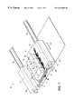
- FIG. 2is an isometric view of a silicon wafer containing on the surface thereof a plurality of the magnetic actuated ink jet printing devices of FIG. 1, and showing the dicing lines for separating the devices;
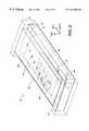
- FIG. 3is a single magnetic actuated ink jet printing device shown in isometric view after separation from the wafer in FIG. 2;
- FIGS. 4-6show the fabrication process of only one of the plurality of magnetic actuated ink jet printing devices in the wafer of FIG. 2 in cross-sectional view;
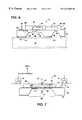
- FIG. 7is a schematic cross-sectional view of a magnetic actuated ink jet printing device disclosing the operating principal thereof;
- FIG. 8is a bottom view of a magnetic actuated ink jet printing device
- FIG. 9is a top view of a magnetic actuated ink jet printing device
- FIG. 10is a cross-sectional view of another embodiment of the magnetic actuated ink jet printing device similar to the view shown in FIG. 6;
- FIG. 11is an isometric view of a multicolor magnetic actuated ink jet printing device, wherein four arrays of nozzles are fabricated in a single printing device;
- FIG. 12is a bottom view of the magnetic actuated ink jet printing device of FIG. 11;
- FIG. 13is a plan view of an alternate embodiment of the electrode covering the diaphragm of the magnetic actuated ink jet printing device which actuates the device and ejects the droplet;
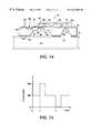
- FIG. 14is a cross-sectional view of an alternate embodiment of the magnetic actuated ink jet printing device and is similar to the cross-sectional view of FIG. 6;
- FIG. 15is a waveform of the current through the electrode on the diaphragm in one embodiment of the magnetic actuated ink jet printing device, showing a continuous current which is increased and decreased to eject an ink droplet.
- FIG. 1a schematic isometric view of a multicolor ink jet printer 10 is partially shown having the magnetic actuated ink jet printing devices 12 of the present invention shown in dashed line.
- the multicolor printercomprises four print cartridges 14 , one for each color and each with an integral printing device 12 , releasably mounted on a translatable carriage 16 .
- the print cartridgeshave an ink supply manifold 18 and ink inlet connectors 20 for the attachment of ink supply tubes (not shown) which provide means for maintaining the manifolds filled with ink from a main supply (not shown) located elsewhere in the printer.
- the carriagehas a frame 22 on which the cartridges are mounted with slidable guides 24 that travel along guide rails 26 under control of a printer controller (not shown) in the back and forth direction of arrow 27 .
- the printing devices or printheadsprint swaths of images on a recording medium 28 , such as paper, with droplets 30 of ink ejected from the printing device nozzles, not shown in this view.
- the recording mediumis held stationary while each swath of image is being printed and then the recording medium is stepped the distance generally equal to the height of the printed swath of image in a direction orthogonal to the carriage translation direction as depicted by arrow 29 .
- the printing deviceseject droplets on demand via ribbon cables 31 from the printer controller.
- the printheadcan be enlarged to cover an entire pagewidth by increasing the number of droplet ejectors.
- the printhead(not shown) can be held stationary while the medium is moved at a constant velocity past it. Such a pagewidth array greatly increases the productivity of the printer.
- the printing device 12comprises a silicon plate 32 having two parallel surfaces 33 , 34 .
- the silicon plateis a portion of a (100) silicon wafer having a thickness of about 20 mils or 500 ⁇ m and is anisotropically etched from the surface 34 to provide a recess 36 therein.
- a glass or ceramic laminate(not shown) could be used instead of the silicon wafer and the recess 36 therein provided by an appropriate process, including, for example, by molding or laser ablation.
- the recess 36has a bottom surface 37 which is substantially parallel to the silicon plate surface 33 and spaced a predetermined distance therefrom, preferably about 1 ⁇ m, in order to form a relatively thin silicon membrane for use as a diaphragm 38 .
- the surface area of the recess bottom surface and thus the area surface of the diaphragmis predetermined to permit the appropriate deformation, and in the preferred embodiment is about 320 ⁇ m square or, if circular, about 320 ⁇ m in diameter.
- the silicon plate top surface 33has an aluminum electrode 40 deposited thereon and aligned so that a portion of the electrode lies over the diaphragm.
- the electrodecould be deposited on the silicon plate bottom surface 34 and recess 36 and aligned so that a portion of the electrode lies on the underside of the diaphragm.
- a nozzle plate 44is formed on silicon plate surface 33 which has an internal cavity 49 therein. The cavity is open against the silicon plate surface and is aligned with the diaphragm and overlying or underlying electrode.
- the nozzle platehas a nozzle 46 which is centrally aligned with the diaphragm.
- the cavityis filled with ink 43 through an inlet (not shown).
- First electric current pulses “I”are selectively applied to the electrode 40 via a transistor 42 which may be integrally formed on the silicon plate surface.
- a predetermined magnetic field B(not shown), which has a field direction extending upward from the surface of the drawing in FIG. 7, causes a force F to be generated whenever a predetermined current passes through the electrode from left to right in FIG. 7, as illustrated by the X,Y,Z coordinates, wherein the force F is the Y direction, the current I is the X direction, and the magnet field B is the Z direction.
- the generated force Fdeforms the diaphragm in the upward direction towards nozzle 46 , as shown in dashed line, thereby increasing the pressure on the ink in the cavity, which serves as an ink reservoir, initiating the ink ejection process.
- a droplet 30is ejected from nozzle 46 when, after the diaphragm moves toward the nozzle, the diaphragm moves in direction away from the nozzle, as when current is removed from the electrode.
- the droplet volume or sizemay by varied by applying an appropriately timed current pulse in the opposite direction via a second transistor 45 in order to drive the diaphragm in the direction away from the nozzle by an oppositely directed force, thereby immediately increasing the chamber volume rather than decreasing it.
- the basic principal on which this invention is basedis the well known law of physics that a force is generated when a current is passed through a conductor which lies in a magnetic field.
- greyscaleis achieved by increasing the volume of ink in the printhead cavity 49 for larger ejected droplets. This is accomplished by first placing a current pulse through the electrode in a direction to create a force on the diaphragm which deforms the diaphragm away from the nozzle. Thus, the cavity is momentarily enlarged and then a current pulse in the opposite direction produces a force on the diaphragm which deforms the diaphragm towards the nozzle. As the ink moves through the nozzle, the current is removed or its direction reversed to enable the diaphragm to return to its original position or be driven back.
- the required pumping pressure at the nozzle 46is given by the following formula:
- the printing devices 12are fabricated using a silicon integrated circuit batch fabrication technique. As shown in FIG. 2, a plurality of magnetic actuated ink jet printing devices or printheads 12 are shown prior to separation into a plurality of individual printing devices. Alternatively, full width array printing devices can be fabricated on large substrates, such as, glass or ceramic composites. In this embodiment, the printing devices are fabricated from a (100) silicon wafer 48 and a layer 50 of photopatternable material, such as, for example, polyimide. The layer of photopatternable material is patterned to form elongated trenches 51 which expose the contact terminals for the electrodes (see FIG. 3 ). Each of the printing devices 12 have an array of nozzles 46 and mutually perpendicular dicing cut lines 52 , shown in dashed lines, which will be subsequently used to separate the printing devices.
- a silicon integrated circuit batch fabrication techniqueAs shown in FIG. 2, a plurality of magnetic actuated ink jet printing devices or printheads 12 are shown prior to separation into a
- a single printing device 12is shown in isometric view in FIG. 3 with two magnetic field generating means (shown in dashed lines), such as, for example, two magnets 54 of sufficient magnetic flux density or field strength on opposing sides thereof.
- Rare earth magnetssuch as cobalt samarium magnets, each having a magnetic field strength of 0.82 Tesla or 8,200 Gauss and located on opposite sides of the printing device with an orientation such that their fields are additive, are sufficient for generating the required droplet ejecting force F for a 600 spi pitch of 42 ⁇ m when electric current pulses of 250 mA are applied to the electrodes on the diaphragm 38 (see FIG. 7 ).
- the printing devicecomprises a portion of a silicon wafer referred to as a silicon plate 32 , electrodes 40 covering a diaphragm for each nozzle 46 , and a patterned layer 50 of photopatternable material, referred to as nozzle plate 44 .
- the cavities 49which serve as ink reservoirs for each nozzle, and a common ink manifold 56 connecting the cavities with inlet 58 are provided by a through etch in the silicon plate and are shown in dashed line.
- the electrode contact terminals 60 , 61 for input and common return, respectively,are shown exposed by the patterning of the nozzle plate.
- a coordinate systemis provided showing the X,Y,Z coordinates as the current I, the force generated direction F, and magnetic field B, respectively.
- FIGS. 4-6show the integrated circuit batch fabrication process for the magnetic actuated ink jet printing devices 12 . Although the fabrication process is on the wafer scale, the portion of the wafer 48 (see FIG. 2) depicted is a cross-sectional view of only one printing device for ease of explanation. In FIG.
- the portion of a n-type (100) silicon waferhereinafter referred to as the silicon plate 32 , has a thickness of about 20 mils (500 ⁇ m) and one surface 33 is doped through one or more masks to form a patterned p-type etch stop 62 for each printing device nozzle having a surface dimension of 320 ⁇ m ⁇ 320 ⁇ m or 320 ⁇ m in diameter and a concentration of about 10 19 Boron ions/cc to a depth of about lam.
- an electrochemical etch stopwhich is well known in the industry, can be used with a much smaller concentration of dopant ions in order to avoid the high stress that is generated in the membrane or diaphragm by a high concentration of Boron ions.
- etch stops 62will subsequently define the flexible diaphragms 38 (see FIGS. 6 and 7) which will be used to eject ink droplets.
- a second area 66 encompassing and surrounding all of the diaphragm etch stops 62is also p-doped to the same concentration, but to a larger depth, namely, 18 ⁇ m. For an eight nozzle printing device, second p-doped area 66 would have a surface area of about 2700 ⁇ m ⁇ 650 ⁇ m.
- a protective, etch resistant layer 63such as, for example, silicon nitride or silicon oxide, having a thickness of about 1000 angstrom to 1 ⁇ m.
- the etch resistant layer 69 on surface 33 of the silicon plateis shown only in the embodiment disclosed in FIG. 14 .
- an integral semiconductor transistor or CMOS switch 42could be formed on the surface 33 of the silicon plate during this stage of the process for use as the switch to selectively apply an electric current to a subsequently formed electrode.
- Metal electrodes 40such as aluminum, is patterned on the silicon plate surface 33 so that each electrode overlies an etch stop 62 and is oriented so that current must flow in a particular direction. In FIG.
- the current flow directionis either left to right or right to left.
- the electrodeis passivated with a passivation layer (not shown), except for the electrode ends used as contact terminals 60 , 61 (also see FIG. 9 ).
- a 20 to 30 ⁇ m thick sacrificial layer 64is deposited and patterned on the surface 33 of the silicon plate and the passivated electrodes 40 thereon.
- a low temperature processis required for the deposition of the sacrificial layer, so that the underlying metal electrodes are not attacked.
- suitable photoresistssuch as, for example, AZ4620TM a commercially available photoresist from Shipley, may be sputtered or spun on to the appropriate depth at a temperature of less than 400° C. which process temperature will not attack the metal electrodes.
- the other requirement of the sacrificial layeris that it must be selectively removed by chemicals which will not attack the nozzle plate material, which in the preferred embodiment is polyimide.
- This sacificial layeris then patterned to build the areas for the ink cavity 49 (see FIGS. 6 and 7) and ink flow passages such as the common manifold 56 (see FIG. 6) and passageways which interconnect the ink cavities 49 to the manifold.
- the next stepis the deposition of one or more layers of a material, such as, for example, a photosensitive polyimide layer 50 to a thickness of about two times that of the sacrificial layer or about 40 to 60 ⁇ m which will later be patterned using typical photolithographic steps to form the nozzle plate 44 .
- an etch resistant layermay be deposited over layer 50 to protect it from a subsequent anisotropic etch.
- the protective, etch resistant layer 63 on the back side surface 34 of the silicon plateis patterned to provide vias 65 therein and an anisotropic etchant is used, such as potassium hydroxide (KOH) or ethylenediamine pyrocatechol (EDP), to etch the recess 36 and through hole 58 with open bottom 59 .
- KOHpotassium hydroxide
- EDPethylenediamine pyrocatechol
- the etch stops 62 , 66prevent further etching.
- the etch stop 62provides the diaphragms 38 .
- the through hole 58will subsequently serve as an ink inlet to the common manifold provided by removal of the sacrificial layer.
- the next stepis to pattern the layer 50 to form the nozzles 46 and nozzle plate 44 and to remove the layer from above the electrode terminals 60 , 61 for access thereto.
- the patterningis done photolithographically by means well known in the industry.
- the sacrificial layer 64is removed using selective wet etch followed by curing the patterned layer 50 if necessary, to form the nozzle plate 44 as shown in FIG. 6 .
- a plurality of printing deviceswould be integrally formed on a four or five inch diameter silicon wafer and the wafer would be diced along the dicing lines 52 (see FIG. 2) to separate the printing devices into a plurality of individual printing devices.
- Each individual printing device 12is then bonded to an ink supply manifold 18 , shown in FIG. 6 in dashed line, with a manifold opening 67 in alignment with the etched through hole 58 , so that ink in the ink supply manifold is in fluid communication with the nozzles 46 in the nozzle plate 44 by way of a flow path through the common manifold 56 and thus to the cavities or ink reservoirs 49 which connect to the nozzles (see also FIG. 3 ).
- printing devices 12could be abutted or staggered for the desire length, or as mentioned above the diaphragm bearing substrate 32 and nozzle plate 44 could be pagewidth in length with the magnetic field generating means 54 spaced along the length of the printing device.
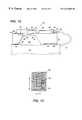
- FIG. 8a bottom view of the magnetic actuated ink jet printing device 12 is shown.
- This printing devicehas been fabricated in accordance with the fabricating process discussed above and as depicted in FIGS. 4-6. Although only eight diaphragms 38 are shown in the silicon plate 32 for clarity, an actual printing device would have many more in an array on a 600 spi spacing.
- the main anisotropically etched recess 36 through silicon plate surface 34is shown which has a depth defined by the etch stop 66 , so that the recess bottom surface 37 is formed at the 18 ⁇ m deep etch stop 66 .
- All of the diaphragms 38are defined by the etch stops 62 , each having the depth of 1 ⁇ m, so that the diaphragms are 1 ⁇ m thick.
- a few of the addressing electrodes 40 , integral transistors 42 , and input terminals 60are shown in dashed line.
- the common return terminal 61Located at one end of the silicon plate is the etched through recess 58 and open bottom 59 which serves as the inlet to the common manifold 56 of the nozzle plate 44 (see FIG. 3 ).
- FIG. 9A top view of the magnetic actuated ink jet printing device 12 is shown in FIG. 9 .
- the nozzles 46are spaced along a column by the center-to-center distance ‘b’ and off set from each other by the dimension ‘a’, so that the array is slightly inclined.
- the ‘b’ distanceis about 320 ⁇ m and the ‘a’ dimension is about 42 ⁇ m.
- the diaphragms 38are shown in dashed line below each nozzle.
- the layer 50 of nozzle plate material, such as polyimide,has been patterned to expose the terminals 60 , 61 on the surface 33 of the silicon plate 32 and to form the nozzles 46 is the nozzle plate 44 .
- the etched ink inlet 59is also shown in dashed line for clarity.
- the magnetic field generating means 54such as for example, permanent magnets are shown in dashed line with the orientation of the magnetic field B indicated by arrows.
- the magnetic field orientationmay be any planar direction, so long as the electrode portions adjacent the diaphragms are within the magnetic field and are perpendicular to the magnetic field direction.
- FIG. 10An alternate embodiment is shown in FIG. 10, which is similar to the cross-sectional view of FIG. 6 .
- the difference between the two embodimentsis that in FIG. 10, the etched through recess 58 with open bottom 59 is omitted and instead the sacrificial layer is patterned to open through the side of the layer 50 of nozzle plate material when it is patterned.
- an open passageway 68penetrates the side 57 of the nozzle plate 44 .
- a hose connection 70is bonded to the nozzle plate and a hose 72 is connected thereto.
- the surface 33 of the silicon plate 32is doped to form the etch stops 62 , 66 to a concentration of 10 19 Boron ions/cc to the respective depths of 1 ⁇ m and 18 ⁇ m.
- the etch resistant protective layer 63 of silicon nitride or silicon oxideis deposited on the bottom surface 34 of the silicon plate.
- the integral transistor or semiconductive switch 42may optionally be produced at this time in the top surface 33 of the silicon plate, followed by patterning the metal electrodes 40 and the deposition of the sacrificial layer 64 (see FIG. 5 ).
- the relatively thick layer of nozzle plate materialis deposited over surface 33 of the silicon plate including the sacrificial layer 64 , followed by the patterning of the protective layer 63 to produce vias 65 for anisotropic etching of the recess 36 which provide the diaphragms 38 .
- the final stepis the patterning of the layer 50 of nozzle plate material to expose the electrode terminals 60 , 61 and produce the nozzles 46 .
- the multicolor printer of FIG. 1has four printing devices of FIG. 3, one for each color of yellow, cyan, magenta, and black.
- FIG. 11shows an isometric view of a multicolor printing device 80 , which differs from that of the single array of nozzles in the printing device of FIG. 3, only in that the four arrays of nozzles are on a single plate 32 , so that alignment of the nozzles for each color is eliminated.
- the size of the plateis larger to accommodate the increased number of electrodes 40 and electrode terminals 60 , 61 and increased number of nozzles and the plate may be any suitable material such as ceramic or glass, but is preferably silicon.
- the nozzle plate material 50is patterned to provide the nozzle plate 44 and the four arrays of nozzles 46 and to expose all of the electrode terminals.
- the magnetic field generating means 54are shown in dashed line and a X,Y,Z coordinate system is shown to depict the orientation of the magnetic fields, the current direction in the electrodes over the diaphragms, and the resultant force F produced which deforms the diaphragms towards and then away from the nozzles to eject the ink droplets.
- FIG. 12A bottom view of the multicolor printing device of FIG. 11 is shown in FIG. 12 .
- four arrays of eight diaphragms eachare shown with each diaphragm 38 having a nozzle 46 shown in dashed line.
- the nozzleshave center-to-center spacings ‘b’ and ‘c’, where ‘b’ is about 320 ⁇ m and ‘c’ is about 640 ⁇ m.
- the off-set of the nozzles in each columnis depicted by the dimension ‘a’ which is the same as that of the single array of nozzles in the printing device of FIG. 3, viz., about 42 ⁇ m.
- the etched recess 36 which is etched to the doped etch stop 66contains in the floor 37 thereof, the arrays of etched recesses which are further etched to the etch stops 62 that define the thickness of the diaphragms 38 .
- the etch stop 66is 18 ⁇ m deep and the etch stop 62 is 1 ⁇ m deep, respectively, from the top surface 33 of the silicon plate 32 , so that the main recess floor 37 is spaced from the top surface of the silicon plate by the thickness of the etch stop 66 and the floor of the recesses which define the diaphragms 38 are spaced from the top surface of the silicon plate by the thickness of the etch stop 62 .
- Reinforcing ribs 86may optionally be provided in the recess 36 by using a separate via (not shown) in the etch resistant layer 63 for each array of diaphragms 38 , so that each array of diaphragms have a separate recess 36 .
- FIG. 13An alternate embodiment of the electrode which lies on the top or bottom of each diaphragm is shown in FIG. 13 .
- the electrodeis two separate coils 82 , 84 of wire patterned over the diaphragm 38 , so that each of the wires pass over the diaphragm several times and a current pulse through the coils of wire pass the current in the same direction.
- Such configuration of wire coilsis often referred to as a “voice coil”.
- the same wirepasses over the diaphragm ten times per pitch and the current in the wires over the diaphragm 38 pass in the same direction as indicated by an arrow representing current direction. Therefore, the current load through the coiled wire is reduced to about 50 mA. This current level is below the typical drive currents of 80 mA used for thermal ink jet printheads, so that current can be switched with transistors in the NMOS technology.
- the current requirementis reduced by a factor of two.
- the current requirementcan be further reduced by an additional factor of two by overlaying a second layer of windings (not shown) in a second layer of metallization (such as typically used in a CMOS process).
- Such an arrangementdoubles the number of wire windings in each pitch from 10 as shown in FIG. 13 to 20 wire crossings on the diaphragm, thus reducing the current requirement by an additional factor of two.
- the required current to eject a dropletcan be decreased to 12.5 mA.
- the current in such an arrangementcan be maintained at 50 mA, so that the force developed thereby is increased by a factor of four.
- the increase in force by a factor of fourwill lead to an increase the deformation of the diaphragm by a factor of four.
- Such an increase in diaphragm deformationmay be desirable to compensate for any low compliance in the walls that form the chamber volume which could lead to a decrease in the ejected drop volume.
- a sheet electrodeis used for simpler layout and processing.
- Bthe magnetic field in Tesla (T)
- ⁇the sheet current density in amps/m 2 .
- Tthe magnetic field in Tesla
- ⁇the sheet current density in amps/m 2
- the force per unit areais 3.33 ⁇ 10 3 N/m 2 .
- the diaphragmwould require an area of 1.5 ⁇ 10 ⁇ 8 m 2 .
- Ithe current
- Rthe resistance of the current carrying sheet.
- the resistance for an aluminum sheet that is about 0.5 ⁇ m thickis approximately 56 m ⁇ .
- EYoung's modulus for polyimide (5 GPa)
- vthe Poisson ratio for polyimide (0.35)
- Young's modulusis 165 GPa and the Poisson ratio is 0.28.
- Young's modulusis 270 GPa and the Poisson ratio is 0.27.
- the required displacementis 0.14 ⁇ m, assuming that the ratio of droplet volume/change in chamber volume equals 1.
- the size of the diaphragmcan be increased as necessary to compensate for any losses in ejected droplet volume due to compliance within the ejection chamber. A small change in the size of the diaphragm leads to a large change in the displacement of the diaphragm since the displacement varies as the fourth power of the size.
- the ejected droplet volumecan also be modulated for gray scale by variation of the magnitude or shape of the current pulse, to provide a larger or smaller diaphragm pressure P, and thus a larger or smaller diaphragm displacement w.
- Droplet modulationcan also be obtained as explained earlier by varying the sign of the current pulse, in order to deflect the diaphragm away from the nozzle in order to increase the chamber volume.
- FIG. 14Another embodiment of the magnetic actuated printing device 12 is shown in FIG. 14 .
- This embodimentis similar to the embodiment shown in FIG. 6, but differs in that the patterned etch stops 62 are omitted, and an etch resistant layer 69 such as silicon nitride, is deposited on the top surface 33 of the silicon plate 32 .
- the etch resistant layer 69is patterned to provide vias 79 to expose the top surface 33 in areas to be subsequently used for the integral transistors 42 and transistors 45 , if used, and the ink inlet 59 .
- the metal electrode 40is formed on the etch resistant layer 69 and exposed silicon plate surface 33 .
- the electrodeis passivated by, for example, a second etch resistant layer of silicon nitride (not shown) thereby sandwiching the electrode between electrically insulating layers.
- a second etch resistant layer of silicon nitride(not shown) thereby sandwiching the electrode between electrically insulating layers.
- the anisotropic etching of the recess 36enables the etching of a second recess 76 .
- the second recess 76is etched completely through the areas no longer protected by the patterned etch stops 62 , so that the diaphragms 38 are provided by the exposed etch resistant layers 69 .
- the etch resistant layermay be removed and replaced with a layer of polyimide or other suitable material for the diaphragm.
- FIG. 15An alternate embodiment of a current waveform is shown in FIG. 15 in which the current is continuous during the printing mode for the magnetic actuated ink jet printing device.
- the diaphragmsare always deformed towards the nozzles as shown in dashed line in FIG. 7 by a continuous current of 100 mA, but droplet ejection takes place only when the current is momentarily increased to, for example, 200 mA increasing the generated force and moving the diaphragm further towards the nozzle and then reduced to, for example, substantially zero, so that each of the diaphragms instantly move in a direction away from the nozzle.
- the ink containing cavities or reservoirs having respective nozzleshave their pressure selectively increased then decreased to expel an ink droplet of predetermined volume.
- the relative timing of increase and decrease of the currentprovides the modulation of the droplet volume and thus grey scale printing.
- the waveformis shown as simple square wave pulses for ease of explaining this embodiment of the invention, a more complex wave form is used in order to control the droplet ejection process.
Landscapes
- Engineering & Computer Science (AREA)
- Manufacturing & Machinery (AREA)
- Particle Formation And Scattering Control In Inkjet Printers (AREA)
Abstract
Description
Claims (27)
Priority Applications (4)
| Application Number | Priority Date | Filing Date | Title |
|---|---|---|---|
| US08/869,946US6234608B1 (en) | 1997-06-05 | 1997-06-05 | Magnetically actuated ink jet printing device |
| JP10151422AJPH10337868A (en) | 1997-06-05 | 1998-06-01 | Magnetic operation ink jet print device and manufacture thereof |
| EP98304334AEP0888888B1 (en) | 1997-06-05 | 1998-06-02 | A magnetically actuated ink jet printing device |
| DE69836519TDE69836519T2 (en) | 1997-06-05 | 1998-06-02 | Magnetically actuated inkjet printing device |
Applications Claiming Priority (1)
| Application Number | Priority Date | Filing Date | Title |
|---|---|---|---|
| US08/869,946US6234608B1 (en) | 1997-06-05 | 1997-06-05 | Magnetically actuated ink jet printing device |
Publications (1)
| Publication Number | Publication Date |
|---|---|
| US6234608B1true US6234608B1 (en) | 2001-05-22 |
Family
ID=25354493
Family Applications (1)
| Application Number | Title | Priority Date | Filing Date |
|---|---|---|---|
| US08/869,946Expired - LifetimeUS6234608B1 (en) | 1997-06-05 | 1997-06-05 | Magnetically actuated ink jet printing device |
Country Status (4)
| Country | Link |
|---|---|
| US (1) | US6234608B1 (en) |
| EP (1) | EP0888888B1 (en) |
| JP (1) | JPH10337868A (en) |
| DE (1) | DE69836519T2 (en) |
Cited By (65)
| Publication number | Priority date | Publication date | Assignee | Title |
|---|---|---|---|---|
| US6481833B1 (en)* | 1999-08-09 | 2002-11-19 | Seiko Epson Corporation | Inkjet printer |
| US20020180857A1 (en)* | 1997-07-15 | 2002-12-05 | Kia Silverbrook | Fluid-dispensing chip |
| US20030030703A1 (en)* | 2001-08-01 | 2003-02-13 | Seiko Epson Corporation | Piezo-electric device and ink cartridge having the same |
| WO2003020523A1 (en)* | 2001-09-04 | 2003-03-13 | Silverbrook Research Pty. Ltd. | Ink supply arrangement for a printer |
| US6629756B2 (en)* | 2001-02-20 | 2003-10-07 | Lexmark International, Inc. | Ink jet printheads and methods therefor |
| US6685302B2 (en) | 2001-10-31 | 2004-02-03 | Hewlett-Packard Development Company, L.P. | Flextensional transducer and method of forming a flextensional transducer |
| US20040027429A1 (en)* | 2000-09-15 | 2004-02-12 | Kia Silverbrook | Printhead assembly having two sets of fluid inlets |
| US20040207694A1 (en)* | 1999-11-15 | 2004-10-21 | Olivetti Tecnost S.P.A. | Monolithic printhead with built-in equipotential network and associated manufacturing method |
| US6821450B2 (en) | 2003-01-21 | 2004-11-23 | Hewlett-Packard Development Company, L.P. | Substrate and method of forming substrate for fluid ejection device |
| US20040239732A1 (en)* | 2001-11-26 | 2004-12-02 | Kia Silverbrook | Ink supply arrangement for a printer |
| US6883903B2 (en) | 2003-01-21 | 2005-04-26 | Martha A. Truninger | Flextensional transducer and method of forming flextensional transducer |
| US20050110842A1 (en)* | 1997-07-15 | 2005-05-26 | Kia Silverbrook | Printhead chip that incorporates micro-mechanical translating mechanisms |
| US20050110839A1 (en)* | 1997-07-15 | 2005-05-26 | Kia Silverbrook | Printhead chip incorporating electro-magnetically operable ink ejection mechanisms |
| US20050129568A1 (en)* | 2003-12-10 | 2005-06-16 | Xerox Corporation | Environmental system including a micromechanical dispensing device |
| US20050127206A1 (en)* | 2003-12-10 | 2005-06-16 | Xerox Corporation | Device and system for dispensing fluids into the atmosphere |
| US20050127207A1 (en)* | 2003-12-10 | 2005-06-16 | Xerox Corporation | Micromechanical dispensing device and a dispensing system including the same |
| US20050130747A1 (en)* | 2003-12-10 | 2005-06-16 | Xerox Corporation | Video game system including a micromechanical dispensing device |
| US20050134152A1 (en)* | 2003-12-18 | 2005-06-23 | Palo Alto Research Center Incorporated | Radially poled piezoelectric diaphragm structures |
| US20050134144A1 (en)* | 2003-12-18 | 2005-06-23 | Palo Alto Research Center Incorporated | Poling system for piezoelectric diaphragm structures |
| US20050134153A1 (en)* | 2003-12-18 | 2005-06-23 | Palo Alto Research Center Incorporated | Piezoelectric diaphragm structure with outer edge electrode |
| US20050168533A1 (en)* | 1997-07-15 | 2005-08-04 | Kia Silverbrook | Printer nozzle for ejecting ink |
| US7052117B2 (en) | 2002-07-03 | 2006-05-30 | Dimatix, Inc. | Printhead having a thin pre-fired piezoelectric layer |
| US20060261481A1 (en)* | 2005-05-19 | 2006-11-23 | Xerox Corporation | Fluid coupler and a device arranged with the same |
| CN1308147C (en)* | 2003-10-31 | 2007-04-04 | 飞赫科技股份有限公司 | How to make an inkjet print head |
| KR100718502B1 (en) | 2005-06-21 | 2007-05-16 | 고려대학교 산학협력단 | Structure of Ink Jet Actuator in Inkjet Printing Head |
| US20070109357A1 (en)* | 2003-06-05 | 2007-05-17 | Samsung Electronics Co., Ltd. | Method of manufacturing a monolithic ink-jet printhead |
| US20070157841A1 (en)* | 2005-12-29 | 2007-07-12 | Yoo Hong S | Patterning method and method for manufacturing liquid crystal display device using the same |
| CN100336663C (en)* | 2003-10-31 | 2007-09-12 | 飞赫科技股份有限公司 | Piezoelectric inkjet head and manufacturing method thereof |
| US20080061163A1 (en)* | 2006-08-28 | 2008-03-13 | Xerox Corporation | Device and system for dispensing fluids into the atmosphere |
| US20080088674A1 (en)* | 2006-10-12 | 2008-04-17 | Canon Kabushiki Kaisha | Ink jet print head and method of manufacturing ink jet print head |
| US20080136867A1 (en)* | 2006-12-12 | 2008-06-12 | Lebens John A | Liquid ejector having improved chamber walls |
| US20100321432A1 (en)* | 2009-06-23 | 2010-12-23 | Xerox Corporation | Ink jet printing systems and methods with pre-fill and dimple design |
| US7950777B2 (en) | 1997-07-15 | 2011-05-31 | Silverbrook Research Pty Ltd | Ejection nozzle assembly |
| US20110169892A1 (en)* | 1997-07-15 | 2011-07-14 | Silverbrook Research Pty Ltd | Inkjet nozzle incorporating actuator with magnetic poles |
| US7988247B2 (en) | 2007-01-11 | 2011-08-02 | Fujifilm Dimatix, Inc. | Ejection of drops having variable drop size from an ink jet printer |
| US8020970B2 (en) | 1997-07-15 | 2011-09-20 | Silverbrook Research Pty Ltd | Printhead nozzle arrangements with magnetic paddle actuators |
| US8025366B2 (en) | 1997-07-15 | 2011-09-27 | Silverbrook Research Pty Ltd | Inkjet printhead with nozzle layer defining etchant holes |
| US8029101B2 (en) | 1997-07-15 | 2011-10-04 | Silverbrook Research Pty Ltd | Ink ejection mechanism with thermal actuator coil |
| US8029102B2 (en) | 1997-07-15 | 2011-10-04 | Silverbrook Research Pty Ltd | Printhead having relatively dimensioned ejection ports and arms |
| US8061812B2 (en) | 1997-07-15 | 2011-11-22 | Silverbrook Research Pty Ltd | Ejection nozzle arrangement having dynamic and static structures |
| US8075104B2 (en) | 1997-07-15 | 2011-12-13 | Sliverbrook Research Pty Ltd | Printhead nozzle having heater of higher resistance than contacts |
| US8083326B2 (en) | 1997-07-15 | 2011-12-27 | Silverbrook Research Pty Ltd | Nozzle arrangement with an actuator having iris vanes |
| US8096642B2 (en) | 1997-08-11 | 2012-01-17 | Silverbrook Research Pty Ltd | Inkjet nozzle with paddle layer arranged between first and second wafers |
| US8102568B2 (en) | 1997-07-15 | 2012-01-24 | Silverbrook Research Pty Ltd | System for creating garments using camera and encoded card |
| US8113629B2 (en) | 1997-07-15 | 2012-02-14 | Silverbrook Research Pty Ltd. | Inkjet printhead integrated circuit incorporating fulcrum assisted ink ejection actuator |
| US8123336B2 (en) | 1997-07-15 | 2012-02-28 | Silverbrook Research Pty Ltd | Printhead micro-electromechanical nozzle arrangement with motion-transmitting structure |
| US8274665B2 (en) | 1997-07-15 | 2012-09-25 | Silverbrook Research Pty Ltd | Image sensing and printing device |
| US8285137B2 (en) | 1997-07-15 | 2012-10-09 | Silverbrook Research Pty Ltd | Digital camera system for simultaneous printing and magnetic recording |
| US8393714B2 (en) | 1997-07-15 | 2013-03-12 | Zamtec Ltd | Printhead with fluid flow control |
| US8421869B2 (en) | 1997-07-15 | 2013-04-16 | Google Inc. | Camera system for with velocity sensor and de-blurring processor |
| US20130097861A1 (en)* | 2011-10-21 | 2013-04-25 | Canon Kabushiki Kaisha | Method for manufacturing inkjet recording head |
| US8459768B2 (en) | 2004-03-15 | 2013-06-11 | Fujifilm Dimatix, Inc. | High frequency droplet ejection device and method |
| US8491076B2 (en) | 2004-03-15 | 2013-07-23 | Fujifilm Dimatix, Inc. | Fluid droplet ejection devices and methods |
| US20140096385A1 (en)* | 2012-10-10 | 2014-04-10 | Canon Kabushiki Kaisha | Method for producing liquid-ejection head |
| US8708441B2 (en) | 2004-12-30 | 2014-04-29 | Fujifilm Dimatix, Inc. | Ink jet printing |
| US8789925B1 (en) | 2013-02-01 | 2014-07-29 | Xerox Corporation | Method and apparatus for printing of magnetic inks |
| US8789939B2 (en) | 1998-11-09 | 2014-07-29 | Google Inc. | Print media cartridge with ink supply manifold |
| US8823823B2 (en) | 1997-07-15 | 2014-09-02 | Google Inc. | Portable imaging device with multi-core processor and orientation sensor |
| US8866923B2 (en) | 1999-05-25 | 2014-10-21 | Google Inc. | Modular camera and printer |
| US8896724B2 (en) | 1997-07-15 | 2014-11-25 | Google Inc. | Camera system to facilitate a cascade of imaging effects |
| US8902333B2 (en) | 1997-07-15 | 2014-12-02 | Google Inc. | Image processing method using sensed eye position |
| US20140356990A1 (en)* | 2013-05-31 | 2014-12-04 | Stmicroelectronics, Inc. | Methods of making inkjet print heads using a sacrificial substrate layer |
| US8908075B2 (en) | 1997-07-15 | 2014-12-09 | Google Inc. | Image capture and processing integrated circuit for a camera |
| US8936196B2 (en) | 1997-07-15 | 2015-01-20 | Google Inc. | Camera unit incorporating program script scanner |
| US20170028467A1 (en)* | 2015-07-28 | 2017-02-02 | Océ-Technologies B.V. | Jetting device |
Families Citing this family (9)
| Publication number | Priority date | Publication date | Assignee | Title |
|---|---|---|---|---|
| KR100213721B1 (en) | 1997-06-28 | 1999-08-02 | 윤종용 | Ink jet device |
| AUPR245401A0 (en)* | 2001-01-10 | 2001-02-01 | Silverbrook Research Pty Ltd | An apparatus (WSM07) |
| GB2375185A (en)* | 2001-05-04 | 2002-11-06 | Kymata Ltd | Thick wafer for MEMS fabrication |
| JP3991894B2 (en)* | 2002-03-18 | 2007-10-17 | セイコーエプソン株式会社 | Piezoelectric actuator manufacturing method, liquid jet head manufacturing method, and actuator base member |
| US6896360B2 (en)* | 2002-10-31 | 2005-05-24 | Hewlett-Packard Development Company, L.P. | Barrier feature in fluid channel |
| JP3912267B2 (en) | 2002-11-29 | 2007-05-09 | ソニー株式会社 | Droplet ejection apparatus, inspection chip processing apparatus, droplet ejection method, inspection chip processing method |
| GB0606685D0 (en) | 2006-04-03 | 2006-05-10 | Xaar Technology Ltd | Droplet Deposition Apparatus |
| JP2009073087A (en)* | 2007-09-21 | 2009-04-09 | Seiko Epson Corp | Actuator device and liquid jet head |
| US20090088618A1 (en) | 2007-10-01 | 2009-04-02 | Arneson Michael R | System and Method for Manufacturing a Swallowable Sensor Device |
Citations (9)
| Publication number | Priority date | Publication date | Assignee | Title |
|---|---|---|---|---|
| JPH04129745A (en) | 1990-09-21 | 1992-04-30 | Seiko Epson Corp | inkjet head |
| JPH04129744A (en) | 1990-09-21 | 1992-04-30 | Seiko Epson Corp | Ink jet head |
| JPH04327945A (en) | 1991-04-26 | 1992-11-17 | Rohm Co Ltd | Ink jet printing head |
| EP0580283A2 (en) | 1992-06-05 | 1994-01-26 | Seiko Epson Corporation | Ink jet head and method of manufacturing thereof |
| US5322594A (en) | 1993-07-20 | 1994-06-21 | Xerox Corporation | Manufacture of a one piece full width ink jet printing bar |
| WO1996032285A1 (en) | 1995-04-12 | 1996-10-17 | Eastman Kodak Company | A self-aligned construction and manufacturing process for monolithic print heads |
| US5818473A (en)* | 1993-07-14 | 1998-10-06 | Seiko Epson Corporation | Drive method for an electrostatic ink jet head for eliminating residual charge in the diaphragm |
| US5854644A (en)* | 1995-10-13 | 1998-12-29 | Samsung Electronics Co., Ltd. | Electromagnetic ink-jet printhead for image forming apparatus |
| US5889541A (en)* | 1996-10-09 | 1999-03-30 | Xerox Corporation | Two-dimensional print cell array apparatus and method for delivery of toner for printing images |
Family Cites Families (8)
| Publication number | Priority date | Publication date | Assignee | Title |
|---|---|---|---|---|
| DE3378966D1 (en) | 1982-05-28 | 1989-02-23 | Xerox Corp | Pressure pulse droplet ejector and array |
| DE3445720A1 (en) | 1984-12-14 | 1986-06-19 | Siemens AG, 1000 Berlin und 8000 München | ARRANGEMENT FOR THE EMISSION OF SINGLE DROPLES FROM THE SPLIT OPENINGS OF AN INK WRITING HEAD |
| DE3500985A1 (en) | 1985-01-14 | 1986-07-17 | Siemens AG, 1000 Berlin und 8000 München | ARRANGEMENT FOR PRODUCING SINGLE DROPLES IN INK WRITING DEVICES |
| US4638337A (en) | 1985-08-02 | 1987-01-20 | Xerox Corporation | Thermal ink jet printhead |
| US4751530A (en) | 1986-12-19 | 1988-06-14 | Xerox Corporation | Acoustic lens arrays for ink printing |
| US4845517A (en) | 1988-01-11 | 1989-07-04 | Am International, Inc. | Droplet deposition apparatus |
| US4983883A (en) | 1989-04-04 | 1991-01-08 | Roland George R | Automatic illumination circuit |
| RU1831438C (en) | 1991-02-22 | 1993-07-30 | С.Н.Максимовский и Г.А.Радуцкий | Jetting printing head |
- 1997
- 1997-06-05USUS08/869,946patent/US6234608B1/ennot_activeExpired - Lifetime
- 1998
- 1998-06-01JPJP10151422Apatent/JPH10337868A/enactivePending
- 1998-06-02EPEP98304334Apatent/EP0888888B1/ennot_activeExpired - Lifetime
- 1998-06-02DEDE69836519Tpatent/DE69836519T2/ennot_activeExpired - Lifetime
Patent Citations (9)
| Publication number | Priority date | Publication date | Assignee | Title |
|---|---|---|---|---|
| JPH04129745A (en) | 1990-09-21 | 1992-04-30 | Seiko Epson Corp | inkjet head |
| JPH04129744A (en) | 1990-09-21 | 1992-04-30 | Seiko Epson Corp | Ink jet head |
| JPH04327945A (en) | 1991-04-26 | 1992-11-17 | Rohm Co Ltd | Ink jet printing head |
| EP0580283A2 (en) | 1992-06-05 | 1994-01-26 | Seiko Epson Corporation | Ink jet head and method of manufacturing thereof |
| US5818473A (en)* | 1993-07-14 | 1998-10-06 | Seiko Epson Corporation | Drive method for an electrostatic ink jet head for eliminating residual charge in the diaphragm |
| US5322594A (en) | 1993-07-20 | 1994-06-21 | Xerox Corporation | Manufacture of a one piece full width ink jet printing bar |
| WO1996032285A1 (en) | 1995-04-12 | 1996-10-17 | Eastman Kodak Company | A self-aligned construction and manufacturing process for monolithic print heads |
| US5854644A (en)* | 1995-10-13 | 1998-12-29 | Samsung Electronics Co., Ltd. | Electromagnetic ink-jet printhead for image forming apparatus |
| US5889541A (en)* | 1996-10-09 | 1999-03-30 | Xerox Corporation | Two-dimensional print cell array apparatus and method for delivery of toner for printing images |
Cited By (201)
| Publication number | Priority date | Publication date | Assignee | Title |
|---|---|---|---|---|
| US8902340B2 (en) | 1997-07-12 | 2014-12-02 | Google Inc. | Multi-core image processor for portable device |
| US9544451B2 (en) | 1997-07-12 | 2017-01-10 | Google Inc. | Multi-core image processor for portable device |
| US9338312B2 (en) | 1997-07-12 | 2016-05-10 | Google Inc. | Portable handheld device with multi-core image processor |
| US8947592B2 (en) | 1997-07-12 | 2015-02-03 | Google Inc. | Handheld imaging device with image processor provided with multiple parallel processing units |
| US20100182379A1 (en)* | 1997-07-15 | 2010-07-22 | Silverbrook Research Pty Ltd | Fluid-ejecting integrated circuit utilizing electromagnetic displacement |
| US8908051B2 (en) | 1997-07-15 | 2014-12-09 | Google Inc. | Handheld imaging device with system-on-chip microcontroller incorporating on shared wafer image processor and image sensor |
| US9584681B2 (en) | 1997-07-15 | 2017-02-28 | Google Inc. | Handheld imaging device incorporating multi-core image processor |
| US9560221B2 (en) | 1997-07-15 | 2017-01-31 | Google Inc. | Handheld imaging device with VLIW image processor |
| US20020180857A1 (en)* | 1997-07-15 | 2002-12-05 | Kia Silverbrook | Fluid-dispensing chip |
| US9432529B2 (en) | 1997-07-15 | 2016-08-30 | Google Inc. | Portable handheld device with multi-core microcoded image processor |
| US9237244B2 (en) | 1997-07-15 | 2016-01-12 | Google Inc. | Handheld digital camera device with orientation sensing and decoding capabilities |
| US9219832B2 (en) | 1997-07-15 | 2015-12-22 | Google Inc. | Portable handheld device with multi-core image processor |
| US9197767B2 (en) | 1997-07-15 | 2015-11-24 | Google Inc. | Digital camera having image processor and printer |
| US9191529B2 (en) | 1997-07-15 | 2015-11-17 | Google Inc | Quad-core camera processor |
| US6820968B2 (en)* | 1997-07-15 | 2004-11-23 | Silverbrook Research Pty Ltd | Fluid-dispensing chip |
| US9191530B2 (en) | 1997-07-15 | 2015-11-17 | Google Inc. | Portable hand-held device having quad core image processor |
| US9185247B2 (en) | 1997-07-15 | 2015-11-10 | Google Inc. | Central processor with multiple programmable processor units |
| US9185246B2 (en) | 1997-07-15 | 2015-11-10 | Google Inc. | Camera system comprising color display and processor for decoding data blocks in printed coding pattern |
| US9179020B2 (en) | 1997-07-15 | 2015-11-03 | Google Inc. | Handheld imaging device with integrated chip incorporating on shared wafer image processor and central processor |
| US20050110842A1 (en)* | 1997-07-15 | 2005-05-26 | Kia Silverbrook | Printhead chip that incorporates micro-mechanical translating mechanisms |
| US20050110839A1 (en)* | 1997-07-15 | 2005-05-26 | Kia Silverbrook | Printhead chip incorporating electro-magnetically operable ink ejection mechanisms |
| US20050110837A1 (en)* | 1997-07-15 | 2005-05-26 | Kia Silverbrook | Micro-electromechanical device for dispensing fluid |
| US9168761B2 (en) | 1997-07-15 | 2015-10-27 | Google Inc. | Disposable digital camera with printing assembly |
| US9148530B2 (en) | 1997-07-15 | 2015-09-29 | Google Inc. | Handheld imaging device with multi-core image processor integrating common bus interface and dedicated image sensor interface |
| US9143636B2 (en) | 1997-07-15 | 2015-09-22 | Google Inc. | Portable device with dual image sensors and quad-core processor |
| US9143635B2 (en) | 1997-07-15 | 2015-09-22 | Google Inc. | Camera with linked parallel processor cores |
| US9137398B2 (en) | 1997-07-15 | 2015-09-15 | Google Inc. | Multi-core processor for portable device with dual image sensors |
| US9137397B2 (en) | 1997-07-15 | 2015-09-15 | Google Inc. | Image sensing and printing device |
| US9131083B2 (en) | 1997-07-15 | 2015-09-08 | Google Inc. | Portable imaging device with multi-core processor |
| US9124737B2 (en) | 1997-07-15 | 2015-09-01 | Google Inc. | Portable device with image sensor and quad-core processor for multi-point focus image capture |
| US9124736B2 (en) | 1997-07-15 | 2015-09-01 | Google Inc. | Portable hand-held device for displaying oriented images |
| US9060128B2 (en) | 1997-07-15 | 2015-06-16 | Google Inc. | Portable hand-held device for manipulating images |
| US9055221B2 (en) | 1997-07-15 | 2015-06-09 | Google Inc. | Portable hand-held device for deblurring sensed images |
| US8953061B2 (en) | 1997-07-15 | 2015-02-10 | Google Inc. | Image capture device with linked multi-core processor and orientation sensor |
| US8953178B2 (en) | 1997-07-15 | 2015-02-10 | Google Inc. | Camera system with color display and processor for reed-solomon decoding |
| US20050168533A1 (en)* | 1997-07-15 | 2005-08-04 | Kia Silverbrook | Printer nozzle for ejecting ink |
| US8953060B2 (en) | 1997-07-15 | 2015-02-10 | Google Inc. | Hand held image capture device with multi-core processor and wireless interface to input device |
| US8947679B2 (en) | 1997-07-15 | 2015-02-03 | Google Inc. | Portable handheld device with multi-core microcoded image processor |
| US8936196B2 (en) | 1997-07-15 | 2015-01-20 | Google Inc. | Camera unit incorporating program script scanner |
| US8937727B2 (en) | 1997-07-15 | 2015-01-20 | Google Inc. | Portable handheld device with multi-core image processor |
| US8934053B2 (en) | 1997-07-15 | 2015-01-13 | Google Inc. | Hand-held quad core processing apparatus |
| US8934027B2 (en) | 1997-07-15 | 2015-01-13 | Google Inc. | Portable device with image sensors and multi-core processor |
| US8928897B2 (en) | 1997-07-15 | 2015-01-06 | Google Inc. | Portable handheld device with multi-core image processor |
| US20060066680A1 (en)* | 1997-07-15 | 2006-03-30 | Silverbrook Research Pty Ltd | Micro-electromechanical liquid ejection device with motion amplification |
| US7040738B2 (en)* | 1997-07-15 | 2006-05-09 | Silverbrook Research Pty Ltd | Printhead chip that incorporates micro-mechanical translating mechanisms |
| US8922791B2 (en) | 1997-07-15 | 2014-12-30 | Google Inc. | Camera system with color display and processor for Reed-Solomon decoding |
| US8922670B2 (en) | 1997-07-15 | 2014-12-30 | Google Inc. | Portable hand-held device having stereoscopic image camera |
| US8913137B2 (en) | 1997-07-15 | 2014-12-16 | Google Inc. | Handheld imaging device with multi-core image processor integrating image sensor interface |
| US8913182B2 (en) | 1997-07-15 | 2014-12-16 | Google Inc. | Portable hand-held device having networked quad core processor |
| US7083264B2 (en)* | 1997-07-15 | 2006-08-01 | Silverbrook Research Pty Ltd | Micro-electromechanical liquid ejection device with motion amplification |
| US8913151B2 (en) | 1997-07-15 | 2014-12-16 | Google Inc. | Digital camera with quad core processor |
| US7097285B2 (en)* | 1997-07-15 | 2006-08-29 | Silverbrook Research Pty Ltd | Printhead chip incorporating electro-magnetically operable ink ejection mechanisms |
| US20060232631A1 (en)* | 1997-07-15 | 2006-10-19 | Silverbrook Research Pty Ltd | MEMS device with movement amplifying actuator |
| US8908075B2 (en) | 1997-07-15 | 2014-12-09 | Google Inc. | Image capture and processing integrated circuit for a camera |
| US7140723B2 (en) | 1997-07-15 | 2006-11-28 | Silverbrook Research Pty Ltd | Micro-electromechanical device for dispensing fluid |
| US20060273691A1 (en)* | 1997-07-15 | 2006-12-07 | Silverbrook Research Pty Ltd | Micro-electromechanical ink ejection mechanism utilizing through-wafer ink ejection |
| US8908069B2 (en) | 1997-07-15 | 2014-12-09 | Google Inc. | Handheld imaging device with quad-core image processor integrating image sensor interface |
| US8902357B2 (en) | 1997-07-15 | 2014-12-02 | Google Inc. | Quad-core image processor |
| US20070035585A1 (en)* | 1997-07-15 | 2007-02-15 | Silverbrook Research Pty Ltd | Fluid-ejecting integrated circuit utilizing electromagnetic displacement |
| US8902324B2 (en) | 1997-07-15 | 2014-12-02 | Google Inc. | Quad-core image processor for device with image display |
| US8902333B2 (en) | 1997-07-15 | 2014-12-02 | Google Inc. | Image processing method using sensed eye position |
| US8896720B2 (en) | 1997-07-15 | 2014-11-25 | Google Inc. | Hand held image capture device with multi-core processor for facial detection |
| US7201471B2 (en) | 1997-07-15 | 2007-04-10 | Silverbrook Research Pty Ltd | MEMS device with movement amplifying actuator |
| US8896724B2 (en) | 1997-07-15 | 2014-11-25 | Google Inc. | Camera system to facilitate a cascade of imaging effects |
| US8866926B2 (en) | 1997-07-15 | 2014-10-21 | Google Inc. | Multi-core processor for hand-held, image capture device |
| US7219982B2 (en)* | 1997-07-15 | 2007-05-22 | Silverbrook Research Pty Ltd | Printer nozzle for ejecting ink |
| US8836809B2 (en) | 1997-07-15 | 2014-09-16 | Google Inc. | Quad-core image processor for facial detection |
| US8823823B2 (en) | 1997-07-15 | 2014-09-02 | Google Inc. | Portable imaging device with multi-core processor and orientation sensor |
| US8421869B2 (en) | 1997-07-15 | 2013-04-16 | Google Inc. | Camera system for with velocity sensor and de-blurring processor |
| US20070171255A1 (en)* | 1997-07-15 | 2007-07-26 | Silverbrook Research Pty Ltd | Nozzle arrangement with thermally operated ink ejection piston |
| US8393714B2 (en) | 1997-07-15 | 2013-03-12 | Zamtec Ltd | Printhead with fluid flow control |
| US8287105B2 (en) | 1997-07-15 | 2012-10-16 | Zamtec Limited | Nozzle arrangement for an inkjet printhead having an ink ejecting roof structure |
| US8285137B2 (en) | 1997-07-15 | 2012-10-09 | Silverbrook Research Pty Ltd | Digital camera system for simultaneous printing and magnetic recording |
| US8274665B2 (en) | 1997-07-15 | 2012-09-25 | Silverbrook Research Pty Ltd | Image sensing and printing device |
| US8123336B2 (en) | 1997-07-15 | 2012-02-28 | Silverbrook Research Pty Ltd | Printhead micro-electromechanical nozzle arrangement with motion-transmitting structure |
| US8113629B2 (en) | 1997-07-15 | 2012-02-14 | Silverbrook Research Pty Ltd. | Inkjet printhead integrated circuit incorporating fulcrum assisted ink ejection actuator |
| US8102568B2 (en) | 1997-07-15 | 2012-01-24 | Silverbrook Research Pty Ltd | System for creating garments using camera and encoded card |
| US8083326B2 (en) | 1997-07-15 | 2011-12-27 | Silverbrook Research Pty Ltd | Nozzle arrangement with an actuator having iris vanes |
| US8075104B2 (en) | 1997-07-15 | 2011-12-13 | Sliverbrook Research Pty Ltd | Printhead nozzle having heater of higher resistance than contacts |
| US8061812B2 (en) | 1997-07-15 | 2011-11-22 | Silverbrook Research Pty Ltd | Ejection nozzle arrangement having dynamic and static structures |
| US8029102B2 (en) | 1997-07-15 | 2011-10-04 | Silverbrook Research Pty Ltd | Printhead having relatively dimensioned ejection ports and arms |
| US8029101B2 (en) | 1997-07-15 | 2011-10-04 | Silverbrook Research Pty Ltd | Ink ejection mechanism with thermal actuator coil |
| US8025366B2 (en) | 1997-07-15 | 2011-09-27 | Silverbrook Research Pty Ltd | Inkjet printhead with nozzle layer defining etchant holes |
| US8020970B2 (en) | 1997-07-15 | 2011-09-20 | Silverbrook Research Pty Ltd | Printhead nozzle arrangements with magnetic paddle actuators |
| US7988262B2 (en) | 1997-07-15 | 2011-08-02 | Silverbrook Research Pty Ltd | Fluid-ejecting integrated circuit utilizing electromagnetic displacement |
| US7387365B2 (en) | 1997-07-15 | 2008-06-17 | Silverbrook Research Pty Ltd | Nozzle for an inkjet printer incorporating a plunger assembly |
| US20080165226A1 (en)* | 1997-07-15 | 2008-07-10 | Silverbrook Research Pty Ltd | Nozzle assembly having a sprung electromagnetically operated plunger |
| US20110169892A1 (en)* | 1997-07-15 | 2011-07-14 | Silverbrook Research Pty Ltd | Inkjet nozzle incorporating actuator with magnetic poles |
| US7448728B2 (en) | 1997-07-15 | 2008-11-11 | Silverbrook Research Pty Ltd | Nozzle assembly having a sprung electromagnetically operated plunger |
| US7465026B2 (en) | 1997-07-15 | 2008-12-16 | Silverbrook Research Pty Ltd | Nozzle arrangement with thermally operated ink ejection piston |
| US7950777B2 (en) | 1997-07-15 | 2011-05-31 | Silverbrook Research Pty Ltd | Ejection nozzle assembly |
| US7934797B2 (en) | 1997-07-15 | 2011-05-03 | Silverbrook Research Pty Ltd | Printhead with reciprocating coils |
| US20090027448A1 (en)* | 1997-07-15 | 2009-01-29 | Silverbrook Research Pty Ltd | Printhead with reciprocating coils |
| US7695108B2 (en) | 1997-07-15 | 2010-04-13 | Silverbrook Research Pty Ltd | Fluid-ejecting integrated circuit utilizing electromagnetic displacement |
| US20090085976A1 (en)* | 1997-07-15 | 2009-04-02 | Silverbrook Research Pty Ltd | Nozzle arrangement for an inkjet printhead having an ink ejecting roof structure |
| US7549728B2 (en) | 1997-07-15 | 2009-06-23 | Silverbrook Research Pty Ltd | Micro-electromechanical ink ejection mechanism utilizing through-wafer ink ejection |
| US8096642B2 (en) | 1997-08-11 | 2012-01-17 | Silverbrook Research Pty Ltd | Inkjet nozzle with paddle layer arranged between first and second wafers |
| US8789939B2 (en) | 1998-11-09 | 2014-07-29 | Google Inc. | Print media cartridge with ink supply manifold |
| US8866923B2 (en) | 1999-05-25 | 2014-10-21 | Google Inc. | Modular camera and printer |
| US6481833B1 (en)* | 1999-08-09 | 2002-11-19 | Seiko Epson Corporation | Inkjet printer |
| US20040207694A1 (en)* | 1999-11-15 | 2004-10-21 | Olivetti Tecnost S.P.A. | Monolithic printhead with built-in equipotential network and associated manufacturing method |
| US7279111B2 (en)* | 1999-11-15 | 2007-10-09 | Telecom Italia S.P.A. | Monolithic printhead with built-in equipotential network and associated manufacturing method |
| US6652078B2 (en) | 2000-05-23 | 2003-11-25 | Silverbrook Research Pty Ltd | Ink supply arrangement for a printer |
| US8075112B2 (en) | 2000-05-23 | 2011-12-13 | Silverbrook Research Pty Ltd | Printhead assembly with air cleaning arrangement |
| US7044577B2 (en) | 2000-05-23 | 2006-05-16 | Silverbrook Research Pty Ltd | Printer having a rotary platen assembly for supporting print media |
| US6984016B2 (en) | 2000-05-23 | 2006-01-10 | Silverbrook Research Pty. Ltd. | Self-cleaning inkjet printhead assembly |
| US20050225611A1 (en)* | 2000-05-23 | 2005-10-13 | Silverbrook Research Pty Ltd. | Printer with a self-cleaning inkjet printhead assembly |
| US7467859B2 (en) | 2000-05-23 | 2008-12-23 | Silverbrook Research Pty Ltd | Pagewidth printhead assembly with ink distribution arrangement |
| US20050219307A1 (en)* | 2000-05-23 | 2005-10-06 | Silverbrook Research Pty Ltd | Printer having a rotary platen assembly for supporting print media |
| US7931358B2 (en) | 2000-05-23 | 2011-04-26 | Silverbrook Research Pty Ltd | Pagewidth printhead assembly with top-fed ink ducts |
| US7284817B2 (en) | 2000-05-23 | 2007-10-23 | Silverbrook Research Pty Ltd | Printer with a self-cleaning inkjet printhead assembly |
| US20090066765A1 (en)* | 2000-05-23 | 2009-03-12 | Silverbrook Research Pty Ltd | Pagewidth Printhead Assembly With Top-Fed Ink Ducts |
| US20040095424A1 (en)* | 2000-05-23 | 2004-05-20 | Silverbrook Research Pty Ltd | Ink jet printer that incorporates an ink distribution assembly |
| US20080018697A1 (en)* | 2000-05-23 | 2008-01-24 | Silverbrook Research Pty Ltd | Printhead assembly with air cleaning arrangement |
| US20040104960A1 (en)* | 2000-05-23 | 2004-06-03 | Silverbrook Research Pty Ltd | Self-cleaning inkjet printhead assembly |
| US7192125B2 (en) | 2000-05-23 | 2007-03-20 | Silverbrook Research Pty Ltd | Ink jet printer that incorporates an ink distribution assembly |
| US20080166171A1 (en)* | 2000-09-15 | 2008-07-10 | Silverbrook Research Pty Ltd | Printer with set spacing between a print engine and an exit roller assembly |
| US20040028445A1 (en)* | 2000-09-15 | 2004-02-12 | Kia Silverbrook | Elongate printhead assembly including multiple fluid supply galleries |
| US20090237481A1 (en)* | 2000-09-15 | 2009-09-24 | Silverbrook Research Pty Ltd | Printer Incorporating Partially Arcuate Printhead |
| US7364286B2 (en) | 2000-09-15 | 2008-04-29 | Silverbrook Research Pty Ltd | Print engine incorporating a quartet of printhead modules arranged in pairs |
| US20110199451A1 (en)* | 2000-09-15 | 2011-08-18 | Silverbrook Research Pty Ltd | Printer having arcuate printhead |
| US20080012902A1 (en)* | 2000-09-15 | 2008-01-17 | Silverbrook Research Pty Ltd | Stackable printer module for effecting double-sided printing |
| US8113650B2 (en) | 2000-09-15 | 2012-02-14 | Silverbrook Resesarch Pty Ltd | Printer having arcuate printhead |
| US20040027429A1 (en)* | 2000-09-15 | 2004-02-12 | Kia Silverbrook | Printhead assembly having two sets of fluid inlets |
| US20050140756A1 (en)* | 2000-09-15 | 2005-06-30 | Kia Silverbrook | Printhead assembly having modular ink distribution |
| US7771019B2 (en) | 2000-09-15 | 2010-08-10 | Silverbrook Research Pty Ltd | Stackable printer module for effecting double-sided printing |
| US7284822B2 (en) | 2000-09-15 | 2007-10-23 | Silverbrook Research Pty Ltd | Printhead assembly having modular ink distribution |
| US7222940B2 (en) | 2000-09-15 | 2007-05-29 | Silverbrook Research Pty Ltd | Print engine |
| US7222941B2 (en) | 2000-09-15 | 2007-05-29 | Silverbrook Research Pty Ltd | Printer for duplex printing with multiple printhead modules |
| US6966636B2 (en)* | 2000-09-15 | 2005-11-22 | Silverbrook Research Pty Ltd | Elongate printhead assembly including multiple fluid supply galleries |
| US20050157135A1 (en)* | 2000-09-15 | 2005-07-21 | Kia Silverbrook | Print engine |
| US6869172B2 (en)* | 2000-09-15 | 2005-03-22 | Silverbrook Research Pty Ltd | Printhead assembly having two sets of fluid inlets |
| US7556369B2 (en) | 2000-09-15 | 2009-07-07 | Silverbrook Research Pty Ltd | Printer with set spacing between a print engine and an exit roller assembly |
| US7472989B2 (en) | 2000-09-15 | 2009-01-06 | Silverbrook Research Pty Ltd | Print media loading mechanism having displaceable endless belts |
| US7946702B2 (en) | 2000-09-15 | 2011-05-24 | Silverbrook Research Pty Ltd | Printer incorporating partially arcuate printhead |
| US7901067B2 (en) | 2000-09-15 | 2011-03-08 | Silverbrook Research Pty Ltd. | Print media loading mechanism having displaceable endless belts |
| US20050275702A1 (en)* | 2000-09-15 | 2005-12-15 | Silverbrook Research Pty Ltd | Printer for duplex printing with multiple printhead modules |
| US6629756B2 (en)* | 2001-02-20 | 2003-10-07 | Lexmark International, Inc. | Ink jet printheads and methods therefor |
| US6921160B2 (en)* | 2001-08-01 | 2005-07-26 | Seiko Epson Corporation | Piezo-electric device and ink cartridge having the same |
| US20030030703A1 (en)* | 2001-08-01 | 2003-02-13 | Seiko Epson Corporation | Piezo-electric device and ink cartridge having the same |
| WO2003020523A1 (en)* | 2001-09-04 | 2003-03-13 | Silverbrook Research Pty. Ltd. | Ink supply arrangement for a printer |
| US6918647B2 (en) | 2001-09-04 | 2005-07-19 | Silverbrook Research Pty Ltd | Inkjet printhead assembly having a rotary platen assembly |
| US20040095423A1 (en)* | 2001-09-04 | 2004-05-20 | Silverbrook Research Pty Ltd | Inkjet printhead assembly having a rotary platen assembly |
| US20050110816A1 (en)* | 2001-09-04 | 2005-05-26 | Kia Silverbrook | Printhead-to-platen variable spacing mechanism |
| US7178892B2 (en) | 2001-09-04 | 2007-02-20 | Silverbrook Res Pty Ltd | Printhead-to-platen variable spacing mechanism |
| US6685302B2 (en) | 2001-10-31 | 2004-02-03 | Hewlett-Packard Development Company, L.P. | Flextensional transducer and method of forming a flextensional transducer |
| US20040239732A1 (en)* | 2001-11-26 | 2004-12-02 | Kia Silverbrook | Ink supply arrangement for a printer |
| US8162466B2 (en) | 2002-07-03 | 2012-04-24 | Fujifilm Dimatix, Inc. | Printhead having impedance features |
| US7052117B2 (en) | 2002-07-03 | 2006-05-30 | Dimatix, Inc. | Printhead having a thin pre-fired piezoelectric layer |
| US7303264B2 (en) | 2002-07-03 | 2007-12-04 | Fujifilm Dimatix, Inc. | Printhead having a thin pre-fired piezoelectric layer |
| US7018015B2 (en) | 2003-01-21 | 2006-03-28 | Hewlett-Packard Development Company, L.P. | Substrate and method of forming substrate for fluid ejection device |
| US7378030B2 (en) | 2003-01-21 | 2008-05-27 | Hewlett-Packard Development Company, L.P. | Flextensional transducer and method of forming flextensional transducer |
| US6821450B2 (en) | 2003-01-21 | 2004-11-23 | Hewlett-Packard Development Company, L.P. | Substrate and method of forming substrate for fluid ejection device |
| US20050157096A1 (en)* | 2003-01-21 | 2005-07-21 | Truninger Martha A. | Flextensional transducer and method of forming flextensional transducer |
| US6883903B2 (en) | 2003-01-21 | 2005-04-26 | Martha A. Truninger | Flextensional transducer and method of forming flextensional transducer |
| US20050088491A1 (en)* | 2003-01-21 | 2005-04-28 | Truninger Martha A. | Substrate and method of forming substrate for fluid ejection device |
| US20070109357A1 (en)* | 2003-06-05 | 2007-05-17 | Samsung Electronics Co., Ltd. | Method of manufacturing a monolithic ink-jet printhead |
| US7334335B2 (en)* | 2003-06-05 | 2008-02-26 | Samsung Electronics Co., Ltd. | Method of manufacturing a monolithic ink-jet printhead |
| CN1308147C (en)* | 2003-10-31 | 2007-04-04 | 飞赫科技股份有限公司 | How to make an inkjet print head |
| CN100336663C (en)* | 2003-10-31 | 2007-09-12 | 飞赫科技股份有限公司 | Piezoelectric inkjet head and manufacturing method thereof |
| US20060186220A1 (en)* | 2003-12-10 | 2006-08-24 | Xerox Corporation | Device and system for dispensing fluids into the atmosphere |
| US20050129568A1 (en)* | 2003-12-10 | 2005-06-16 | Xerox Corporation | Environmental system including a micromechanical dispensing device |
| US20050127206A1 (en)* | 2003-12-10 | 2005-06-16 | Xerox Corporation | Device and system for dispensing fluids into the atmosphere |
| US20050127207A1 (en)* | 2003-12-10 | 2005-06-16 | Xerox Corporation | Micromechanical dispensing device and a dispensing system including the same |
| US20050130747A1 (en)* | 2003-12-10 | 2005-06-16 | Xerox Corporation | Video game system including a micromechanical dispensing device |
| US20060289674A1 (en)* | 2003-12-10 | 2006-12-28 | Xerox Corporation | Device and system for dispensing fluids into the atmosphere |
| US20050134153A1 (en)* | 2003-12-18 | 2005-06-23 | Palo Alto Research Center Incorporated | Piezoelectric diaphragm structure with outer edge electrode |
| US7053532B2 (en) | 2003-12-18 | 2006-05-30 | Palo Alto Research Center Incorporated | Radially poled piezoelectric diaphragm structures |
| US20050200236A1 (en)* | 2003-12-18 | 2005-09-15 | Palo Alto Research Center Incorporated. | Method of fabricating an array of multi-electroded piezoelectric transducers for piezoelectric diaphragm structures |
| US7176600B2 (en) | 2003-12-18 | 2007-02-13 | Palo Alto Research Center Incorporated | Poling system for piezoelectric diaphragm structures |
| US7084555B2 (en) | 2003-12-18 | 2006-08-01 | Palo Alto Research Center Incorporated | Piezoelectric diaphragm structure with outer edge electrode |
| US20050134152A1 (en)* | 2003-12-18 | 2005-06-23 | Palo Alto Research Center Incorporated | Radially poled piezoelectric diaphragm structures |
| US20050134144A1 (en)* | 2003-12-18 | 2005-06-23 | Palo Alto Research Center Incorporated | Poling system for piezoelectric diaphragm structures |
| US7290336B2 (en) | 2003-12-18 | 2007-11-06 | Palo Alto Research Center Incorporated | Method of fabricating an array of multi-electroded piezoelectric transducers for piezoelectric diaphragm structures |
| US8459768B2 (en) | 2004-03-15 | 2013-06-11 | Fujifilm Dimatix, Inc. | High frequency droplet ejection device and method |
| US8491076B2 (en) | 2004-03-15 | 2013-07-23 | Fujifilm Dimatix, Inc. | Fluid droplet ejection devices and methods |
| US9381740B2 (en) | 2004-12-30 | 2016-07-05 | Fujifilm Dimatix, Inc. | Ink jet printing |
| US8708441B2 (en) | 2004-12-30 | 2014-04-29 | Fujifilm Dimatix, Inc. | Ink jet printing |
| US20060261481A1 (en)* | 2005-05-19 | 2006-11-23 | Xerox Corporation | Fluid coupler and a device arranged with the same |
| US7331655B2 (en) | 2005-05-19 | 2008-02-19 | Xerox Corporation | Fluid coupler and a device arranged with the same |
| KR100718502B1 (en) | 2005-06-21 | 2007-05-16 | 고려대학교 산학협력단 | Structure of Ink Jet Actuator in Inkjet Printing Head |
| US8893618B2 (en)* | 2005-12-29 | 2014-11-25 | Lg Display Co., Ltd. | Patterning method and method for manufacturing liquid crystal display device using the same |
| US20070157841A1 (en)* | 2005-12-29 | 2007-07-12 | Yoo Hong S | Patterning method and method for manufacturing liquid crystal display device using the same |
| US20080061163A1 (en)* | 2006-08-28 | 2008-03-13 | Xerox Corporation | Device and system for dispensing fluids into the atmosphere |
| US8562845B2 (en)* | 2006-10-12 | 2013-10-22 | Canon Kabushiki Kaisha | Ink jet print head and method of manufacturing ink jet print head |
| US20080088674A1 (en)* | 2006-10-12 | 2008-04-17 | Canon Kabushiki Kaisha | Ink jet print head and method of manufacturing ink jet print head |
| US7600856B2 (en) | 2006-12-12 | 2009-10-13 | Eastman Kodak Company | Liquid ejector having improved chamber walls |
| US20080136867A1 (en)* | 2006-12-12 | 2008-06-12 | Lebens John A | Liquid ejector having improved chamber walls |
| US7988247B2 (en) | 2007-01-11 | 2011-08-02 | Fujifilm Dimatix, Inc. | Ejection of drops having variable drop size from an ink jet printer |
| US20100321432A1 (en)* | 2009-06-23 | 2010-12-23 | Xerox Corporation | Ink jet printing systems and methods with pre-fill and dimple design |
| US8746848B2 (en) | 2009-06-23 | 2014-06-10 | Xerox Corporation | Ink jet printing systems and methods with pre-fill and dimple design |
| US8393713B2 (en)* | 2009-06-23 | 2013-03-12 | Xerox Corporation | Ink jet printing systems and methods with pre-fill and dimple design |
| US9211707B2 (en)* | 2011-10-21 | 2015-12-15 | Canon Kabushiki Kaisha | Method for manufacturing inkjet recording head |
| US20130097861A1 (en)* | 2011-10-21 | 2013-04-25 | Canon Kabushiki Kaisha | Method for manufacturing inkjet recording head |
| US9139003B2 (en)* | 2012-10-10 | 2015-09-22 | Canon Kabushiki Kaisha | Method for producing liquid-ejection head |
| US20140096385A1 (en)* | 2012-10-10 | 2014-04-10 | Canon Kabushiki Kaisha | Method for producing liquid-ejection head |
| US8789925B1 (en) | 2013-02-01 | 2014-07-29 | Xerox Corporation | Method and apparatus for printing of magnetic inks |
| US9340023B2 (en)* | 2013-05-31 | 2016-05-17 | Stmicroelectronics, Inc. | Methods of making inkjet print heads using a sacrificial substrate layer |
| US20140356990A1 (en)* | 2013-05-31 | 2014-12-04 | Stmicroelectronics, Inc. | Methods of making inkjet print heads using a sacrificial substrate layer |
| US20170028467A1 (en)* | 2015-07-28 | 2017-02-02 | Océ-Technologies B.V. | Jetting device |
| US10052689B2 (en)* | 2015-07-28 | 2018-08-21 | Océ-Technologies B.V. | Jetting device |
Also Published As
| Publication number | Publication date |
|---|---|
| EP0888888A2 (en) | 1999-01-07 |
| JPH10337868A (en) | 1998-12-22 |
| EP0888888A3 (en) | 2000-03-22 |
| EP0888888B1 (en) | 2006-11-29 |
| DE69836519T2 (en) | 2007-09-13 |
| DE69836519D1 (en) | 2007-01-11 |
Similar Documents
| Publication | Publication Date | Title |
|---|---|---|
| US6234608B1 (en) | Magnetically actuated ink jet printing device | |
| USRE32572E (en) | Thermal ink jet printhead and process therefor | |
| Chen et al. | A high-resolution silicon monolithic nozzle array for inkjet printing | |
| US4601777A (en) | Thermal ink jet printhead and process therefor | |
| EP1226944B1 (en) | Fabrication method | |
| US5534900A (en) | Ink-jet recording apparatus | |
| EP1652674B1 (en) | Nozzle plate unit, inkjet print head with the same and method of manufacturing the same | |
| US20020071003A1 (en) | Ink jet head, manufacturing method thereof, and ink jet printing apparatus | |
| EP2173559B1 (en) | Actuator | |
| EP1681169B1 (en) | Piezoelectric inkjet printhead and method of manufacturing the same | |
| JPH11320873A (en) | Inkjet head | |
| WO2003070467A2 (en) | Fluid pumping and droplet deposition apparatus | |
| JP2002254662A (en) | Two processes of trench etching for forming completely integrated thermal ink jet print head | |
| JP2002283580A (en) | Ink supply trench etching technique for completely integrated thermal ink-jet printing head | |
| JP2957562B2 (en) | Ink jet device | |
| JP2000141656A (en) | Ink jet head and method of manufacturing the same | |
| US20080122896A1 (en) | Inkjet printhead with backside power return conductor | |
| EP1393908B1 (en) | Fabricating liquid emission electrostatic device using symmetric mandrel | |
| EP1375149B1 (en) | Microinjector having drive circuit and method for making the same | |
| JP2003118114A (en) | Ink jet head and method of manufacturing the same | |
| JPH0447947A (en) | Ink jet jprinter head | |
| Lee et al. | A micromachined monolithic inkjet print head with dome shape chamber | |
| US7635179B2 (en) | Array printhead with three terminal switching elements | |
| JP2001010036A (en) | Ink jet head, method of manufacturing the same, and ink jet recording apparatus | |
| WO2003070469A1 (en) | Actuation device and use thereof in fluid pumping and droplet deposition |
Legal Events
| Date | Code | Title | Description |
|---|---|---|---|
| AS | Assignment | Owner name:XEROX CORPORATION, CONNECTICUT Free format text:ASSIGNMENT OF ASSIGNORS INTEREST;ASSIGNORS:GENOVESE, FRANK C.;KUBBY, JOEL A.;PEETERS, ERIC;AND OTHERS;REEL/FRAME:008610/0035;SIGNING DATES FROM 19970516 TO 19970522 | |
| STCF | Information on status: patent grant | Free format text:PATENTED CASE | |
| AS | Assignment | Owner name:BANK ONE, NA, AS ADMINISTRATIVE AGENT, ILLINOIS Free format text:SECURITY INTEREST;ASSIGNOR:XEROX CORPORATION;REEL/FRAME:013153/0001 Effective date:20020621 | |
| AS | Assignment | Owner name:JPMORGAN CHASE BANK, AS COLLATERAL AGENT, TEXAS Free format text:SECURITY AGREEMENT;ASSIGNOR:XEROX CORPORATION;REEL/FRAME:015134/0476 Effective date:20030625 Owner name:JPMORGAN CHASE BANK, AS COLLATERAL AGENT,TEXAS Free format text:SECURITY AGREEMENT;ASSIGNOR:XEROX CORPORATION;REEL/FRAME:015134/0476 Effective date:20030625 | |
| FPAY | Fee payment | Year of fee payment:4 | |
| FPAY | Fee payment | Year of fee payment:8 | |
| FPAY | Fee payment | Year of fee payment:12 | |
| AS | Assignment | Owner name:XEROX CORPORATION, CONNECTICUT Free format text:RELEASE BY SECURED PARTY;ASSIGNOR:JPMORGAN CHASE BANK, N.A. AS SUCCESSOR-IN-INTEREST ADMINISTRATIVE AGENT AND COLLATERAL AGENT TO JPMORGAN CHASE BANK;REEL/FRAME:066728/0193 Effective date:20220822 |