US6233046B1 - Method of measuring the thickness of a layer of silicon damaged by plasma etching - Google Patents
Method of measuring the thickness of a layer of silicon damaged by plasma etchingDownload PDFInfo
- Publication number
- US6233046B1 US6233046B1US09/343,207US34320799AUS6233046B1US 6233046 B1US6233046 B1US 6233046B1US 34320799 AUS34320799 AUS 34320799AUS 6233046 B1US6233046 B1US 6233046B1
- Authority
- US
- United States
- Prior art keywords
- silicon
- altered
- thickness
- quantities
- layer
- Prior art date
- Legal status (The legal status is an assumption and is not a legal conclusion. Google has not performed a legal analysis and makes no representation as to the accuracy of the status listed.)
- Expired - Lifetime
Links
- XUIMIQQOPSSXEZ-UHFFFAOYSA-NSiliconChemical compound[Si]XUIMIQQOPSSXEZ-UHFFFAOYSA-N0.000titleclaimsabstractdescription52
- 229910052710siliconInorganic materials0.000titleclaimsabstractdescription52
- 239000010703siliconSubstances0.000titleclaimsabstractdescription52
- 238000000034methodMethods0.000titleclaimsabstractdescription47
- 238000001020plasma etchingMethods0.000titleclaimsdescription9
- 238000005259measurementMethods0.000claimsabstractdescription23
- VYPSYNLAJGMNEJ-UHFFFAOYSA-NSilicium dioxideChemical compoundO=[Si]=OVYPSYNLAJGMNEJ-UHFFFAOYSA-N0.000claimsabstractdescription22
- 235000012239silicon dioxideNutrition0.000claimsabstractdescription11
- 239000000377silicon dioxideSubstances0.000claimsabstractdescription11
- 238000010521absorption reactionMethods0.000claimsabstractdescription5
- 238000004364calculation methodMethods0.000claimsabstractdescription4
- 230000001419dependent effectEffects0.000claimsabstract4
- 235000012431wafersNutrition0.000claimsdescription21
- 229910021421monocrystalline siliconInorganic materials0.000claimsdescription12
- 230000008569processEffects0.000claimsdescription11
- 229910021417amorphous siliconInorganic materials0.000claimsdescription7
- 229910021420polycrystalline siliconInorganic materials0.000claimsdescription7
- 230000003287optical effectEffects0.000claimsdescription6
- 238000012545processingMethods0.000claimsdescription2
- 239000010410layerSubstances0.000description36
- 238000005530etchingMethods0.000description9
- 238000004519manufacturing processMethods0.000description6
- 238000012360testing methodMethods0.000description6
- 230000000694effectsEffects0.000description5
- 230000005684electric fieldEffects0.000description4
- 230000010287polarizationEffects0.000description4
- 239000002344surface layerSubstances0.000description4
- 239000013078crystalSubstances0.000description3
- 239000000758substrateSubstances0.000description3
- 230000008859changeEffects0.000description2
- 229920002120photoresistant polymerPolymers0.000description2
- 238000009832plasma treatmentMethods0.000description2
- 230000004044responseEffects0.000description2
- 230000035945sensitivityEffects0.000description2
- 238000004627transmission electron microscopyMethods0.000description2
- 238000011282treatmentMethods0.000description2
- 238000001069Raman spectroscopyMethods0.000description1
- 230000002411adverseEffects0.000description1
- 238000005280amorphizationMethods0.000description1
- 238000004458analytical methodMethods0.000description1
- 230000005465channelingEffects0.000description1
- 230000006866deteriorationEffects0.000description1
- 230000008030eliminationEffects0.000description1
- 238000003379elimination reactionMethods0.000description1
- 238000000572ellipsometryMethods0.000description1
- 230000005284excitationEffects0.000description1
- 230000002349favourable effectEffects0.000description1
- 229920002313fluoropolymerPolymers0.000description1
- 229910052734heliumInorganic materials0.000description1
- 239000001307heliumSubstances0.000description1
- 239000000463materialSubstances0.000description1
- 230000007246mechanismEffects0.000description1
- 238000012986modificationMethods0.000description1
- 230000004048modificationEffects0.000description1
- 238000002310reflectometryMethods0.000description1
- 239000002356single layerSubstances0.000description1
- 239000007787solidSubstances0.000description1
- 230000003595spectral effectEffects0.000description1
- 238000001228spectrumMethods0.000description1
- 238000010561standard procedureMethods0.000description1
- 229910052724xenonInorganic materials0.000description1
- FHNFHKCVQCLJFQ-UHFFFAOYSA-Nxenon atomChemical compound[Xe]FHNFHKCVQCLJFQ-UHFFFAOYSA-N0.000description1
Images
Classifications
- G—PHYSICS
- G01—MEASURING; TESTING
- G01B—MEASURING LENGTH, THICKNESS OR SIMILAR LINEAR DIMENSIONS; MEASURING ANGLES; MEASURING AREAS; MEASURING IRREGULARITIES OF SURFACES OR CONTOURS
- G01B11/00—Measuring arrangements characterised by the use of optical techniques
- G01B11/02—Measuring arrangements characterised by the use of optical techniques for measuring length, width or thickness
- G01B11/06—Measuring arrangements characterised by the use of optical techniques for measuring length, width or thickness for measuring thickness ; e.g. of sheet material
- G01B11/0616—Measuring arrangements characterised by the use of optical techniques for measuring length, width or thickness for measuring thickness ; e.g. of sheet material of coating
- G01B11/0641—Measuring arrangements characterised by the use of optical techniques for measuring length, width or thickness for measuring thickness ; e.g. of sheet material of coating with measurement of polarization
- G—PHYSICS
- G01—MEASURING; TESTING
- G01N—INVESTIGATING OR ANALYSING MATERIALS BY DETERMINING THEIR CHEMICAL OR PHYSICAL PROPERTIES
- G01N21/00—Investigating or analysing materials by the use of optical means, i.e. using sub-millimetre waves, infrared, visible or ultraviolet light
- G01N21/17—Systems in which incident light is modified in accordance with the properties of the material investigated
- G01N21/21—Polarisation-affecting properties
- G01N21/211—Ellipsometry
Definitions
- the present inventionrelates to methods of investigating the effects of plasma treatments used in the manufacture of electronic devices on monocrystalline silicon and, more particularly, to a method of measuring the thickness of the surface layer of silicon altered by such a treatment.
- One of the most important mechanisms causing damage to the siliconis “amorphization” of the first layers of the monocrystalline silicon crystal lattice due to bombardment by the ionic species of the plasma.
- the extent of the damagedepends substantially on the intrinsic characteristics of the etching equipment and on the process parameters selected on the equipment.
- TWthermal wave
- ⁇ Rvariations in the reflectivity
- Rreflectivity
- ⁇ R/Ra correlation, in arbitrary units, between the damage and the effects on the devices, but is fairly inaccurate because it depends upon the time elapsing between the etching and the measurement, on the crystal excitation frequency, and on temperature.
- a method of measuring thicknesses with the use of an ellipsometer with a monochromatic light sourceis also known.
- the refractive index and the thickness of a layer which is transparent for the wavelength of the sourcecan be obtained with this method.
- For an opaque layerit is possible to obtain only the absorption coefficient (the imaginary portion of the refractive index), but not the thickness.
- This methodcan be used to measure a single layer on a larger substrate, that is, a substrate of a thickness much greater than the layer to be measured, such as a thin layer on a monocrystalline silicon wafer.
- One object of the present inventionis to provide a method of measuring the thickness of a surface layer of silicon damaged by plasma treatments.
- FIG. 1shows, in section, the structure of a surface portion of a silicon wafer according to a model on which the method of the invention is based.
- FIG. 2shows schematically a measurement taken with a spectroscopic ellipsometer in order to implement a method according to the invention.
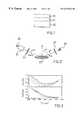
- FIG. 3is a graph showing how two ellipsometric quantities vary in dependence on the wavelength of the measurement light beam of a spectroscopic ellipsometer for different thicknesses of the altered silicon layer.
- FIG. 4is a graph showing the theoretical and experimental curves of two ellipsometric quantities as functions of the wavelength.
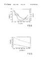
- FIG. 5is a graph which shows the variation of the thickness of a damaged silicon layer in dependence on a parameter of the plasma etching process.
- a monocrystalline silicon waferis preferably subjected to the same treatment to which a similar wafer intended for the manufacture of electronic devices is subjected.
- a layer to be etched with plasmafor example, a silicon dioxide layer, is deposited on the wafer.
- a further stepis carried out to more closely reproduce the actual process conditions precisely, a photoresist mask is formed on the oxide layer.
- the waferis then etched with the same equipment to be used for production wafers or for using test equipment and with the same parameters provided for during the etching of a wafer to be processed to produce actual devices. In particular, the duration of the over-etching will be the same as that provided for in the production process.
- the photoresistis then removed by a standard method, for example, by a first dry removal step and a second wet removal step. This latter step is performed to remove a layer of fluorocarbon polymer which is usually deposited on the silicon surface which has undergone the over-etching.
- the surface structure of the silicon subjected to over-etchingis similar to that shown in section in the model of FIG. 1 : an intact monocrystalline silicon substrate 10 , a damaged silicon layer 11 , and a thin (2-3 nm) native silicon dioxide layer 12 .
- This structureis subjected to measurement with a spectroscopic ellipsometer.
- This known devicemeasures the variation of the state of polarization of a light beam after reflection on the surface of the sample containing the surface layer or layers to be measured.
- the schematic configuration of a spectroscopic ellipsometeris shown in FIG. 2 .
- the light emitted by a white light source 20(usually a xenon lamp which has a fairly continuous spectrum) is polarized linearly by a first polarizer 21 .
- the polarizeris preferably rotated at constant speed.
- the light beam coming from the sourcestrikes the wafer 22 with an angle of incidence usually selected to be close to the Brewster angle of silicon (75°), and is reflected from the silicon with a change in polarization state, that is, a change from linear polarization to elliptical polarization.
- the reflected light beammay be passed through a second polarizer 23 which is mounted in a fixed position (or which, in some devices, is oriented for each wavelength in order to achieve a favourable signal-noise ratio).
- the light signalthen passes through a monochromator 24 in order finally to reach a detector 25 .
- the spectral range of the measurementsis preferably between near UV (about 240 nm) and the near infra-red (about 900 nm).
- r p and r sare reflection coefficients (complex) defined by the ratio between the incident electric field Ei and the reflected electric field Er in the directions parallel and perpendicular to the surface of the sample 22 , respectively.
- a background technical discussionis provided in a publication by R. M. A. Azzam, N. M. Bashara, Ellipsometry and polarized light, North-Holland Publishing Company (1977), with particular reference to pages 269-277.
- FIG. 3shows, for each of the two ellipsometric quantities, four experimental curves corresponding to four different thicknesses of the altered silicon layer 11 after plasma etching performed in different ways.
- the ellipsometric quantities tan ( ⁇ ) and cos ( ⁇ )depend on the refractive index, on the absorption coefficient, and on the thickness of the layer under test, or of each superimposed layer of the sample under test if there is more than one layer.
- the theoretical curves of the ellipsometric quantities with variations of the wavelength of the sourceare calculated from a model of the sample under test by iteration of Fresnel equations. This calculation method is described, in the art, for example, in R. M. A. Azzam, N. M. Bashara, Elliposometry and polarized light, North-Holland Publishing Company (1977), with particular reference to pages 332-340.
- the refractive indices and absorption coefficients of the respective layersare inserted in the Fresnel equations as known parameters.
- the refractive index of monocrystalline silicon and of silicon dioxideare known but the optical characteristics of the damaged silicon layer are not. According to a preferred embodiment of the method of the invention, the hypothesis is made that the damaged layer is described optically as a combination of amorphous silicon and polycrystalline silicon, two materials the refractive indices of which are known.
- ⁇ ais the dielectric function of the first component, in this case the amorphous silicon
- ⁇ pis that of the second component, that is, the polycrystalline silicon
- ⁇is the effective dielectric function of the combination.
- the quantity fis a coefficient which defines the weight of the first component relative to the second in the description of the optical properties of the damaged silicon.
- the theoretical curvesthus define the ellipsometric quantities in dependence on the wavelength of the light source and on three unknown parameters: the thickness of the damaged silicon layer, the thickness of the native oxide layer, and the coefficient f.
- the experimental and theoretical curvesare then compared by means of a “fitting” procedure, for example, the Levenberg-Marquard procedure, which is similar to the least squares method based on the minimization of the deviations with variations of the unknown parameters.
- This methodwhich is described, for example, in Press et al., Numerical recipes in C, The art of scientific computing, Cambridge University Press, New York (1988), can determine which values of these three unknowns render the theoretical and experimental curves superimposable within a given tolerance band.
- FIG. 4shows, by way of example, the experimental curves (dotted lines) of the two ellipsometric measured quantities tan ( ⁇ ) and cos ( ⁇ ) as functions of the wavelengths ⁇ , associated, after a fitting procedure, with the corresponding theoretical curves (continuous lines).
- the values determined for the unknownsare: the thickness of the native oxide layer: 5.1 nm, the thickness of the altered silicon layer: 5.4 nm, and the proportion of amorphous silicon (coefficient f): 62%.
- the measurementscan be taken for any silicon wafer using this technique.
- the measurementcan also be made over the entire surface of the silicon wafer in order to obtain a map of the damaged silicon thickness values.
- This measurement operationcan be performed by the structure and method according to the invention for a silicon wafer within time range on the order of one minute.
- the thickness of the damaged layeris related to a process parameter.
- the variation of the thickness dis shown as a function of the pressure p present in the reactor used for the plasma etching for two different powers.
- resultscan be reported thus very quickly. It can be determined if the quality is within an acceptable range. If analysis of the damage caused by different process steps is desired, it is possible to vary one or more selected process parameters and then perform the measurement on each variation. According to one embodiment, a plurality of wafers can be processed using variations in some parameters and then each tested. A preferred set of process parameters can then be selected which causes the least damage.
- the method according to the inventionhas also been found to be very accurate for measuring two or more superimposed layers and to have high sensitivity (0.1 nm).
- reflection and measurement equipmentcan be used to measure the optical qualities of the silicon stack as shown in FIG. 1, and the results used to determine the thickness of the altered silicon layer.
Landscapes
- Physics & Mathematics (AREA)
- General Physics & Mathematics (AREA)
- Length Measuring Devices By Optical Means (AREA)
Abstract
Description


Claims (7)
Applications Claiming Priority (2)
| Application Number | Priority Date | Filing Date | Title |
|---|---|---|---|
| IT1998MI001504AIT1306911B1 (en) | 1998-06-30 | 1998-06-30 | METHOD FOR MEASURING THE THICKNESS OF A DAMAGED SILICON LAYER WITH PLASMA ATTACHMENTS |
| ITMI98A1504 | 1998-06-30 |
Publications (1)
| Publication Number | Publication Date |
|---|---|
| US6233046B1true US6233046B1 (en) | 2001-05-15 |
Family
ID=11380357
Family Applications (1)
| Application Number | Title | Priority Date | Filing Date |
|---|---|---|---|
| US09/343,207Expired - LifetimeUS6233046B1 (en) | 1998-06-30 | 1999-06-29 | Method of measuring the thickness of a layer of silicon damaged by plasma etching |
Country Status (2)
| Country | Link |
|---|---|
| US (1) | US6233046B1 (en) |
| IT (1) | IT1306911B1 (en) |
Cited By (12)
| Publication number | Priority date | Publication date | Assignee | Title |
|---|---|---|---|---|
| US6411906B1 (en)* | 1998-02-06 | 2002-06-25 | Kabushiki Kaisha Toshiba | Method and system for inspecting polycrystalline semiconductor film |
| US6642066B1 (en) | 2002-05-15 | 2003-11-04 | Advanced Micro Devices, Inc. | Integrated process for depositing layer of high-K dielectric with in-situ control of K value and thickness of high-K dielectric layer |
| US6721051B2 (en)* | 2000-09-20 | 2004-04-13 | Synergetic Technologies, Inc. | Non-intrusive method and apparatus for characterizing particles based on scattering matrix elements measurements using elliptically polarized radiation |
| US20050007592A1 (en)* | 2002-02-18 | 2005-01-13 | Tokyo Electron Limited | Polarization analyzing method |
| US20050009213A1 (en)* | 2003-06-27 | 2005-01-13 | Xinming Wang | Substrate processing method and apparatus |
| US20050018171A1 (en)* | 2003-07-21 | 2005-01-27 | Pierre-Yves Guittet | Noninvasive method for characterizing and identifying embedded micropatterns |
| US20060007430A1 (en)* | 2004-07-09 | 2006-01-12 | Hans-Georg Lotz | Method of determining physical properties of an optical layer or layer system |
| US20070026541A1 (en)* | 2005-07-06 | 2007-02-01 | Fujitsu Limited | Method and system for manufacturing semiconductor device having less variation in electrical characteristics |
| US7179665B1 (en) | 2005-02-17 | 2007-02-20 | Midwest Research Institute | Optical method for determining the doping depth profile in silicon |
| CN102997852A (en)* | 2012-11-14 | 2013-03-27 | 彩虹(张家港)平板显示有限公司 | Glass baseplate bonding line measuring method |
| WO2013003122A3 (en)* | 2011-06-27 | 2013-06-06 | Kla-Tencor Corporation | Measurement of composition for thin films |
| US20230111160A1 (en)* | 2021-10-13 | 2023-04-13 | Changxin Memory Technologies, Inc. | Method for measuring element concentration of material |
Citations (3)
| Publication number | Priority date | Publication date | Assignee | Title |
|---|---|---|---|---|
| US5091320A (en)* | 1990-06-15 | 1992-02-25 | Bell Communications Research, Inc. | Ellipsometric control of material growth |
| US5665214A (en)* | 1995-05-03 | 1997-09-09 | Sony Corporation | Automatic film deposition control method and system |
| US5835221A (en)* | 1995-10-16 | 1998-11-10 | Lucent Technologies Inc. | Process for fabricating a device using polarized light to determine film thickness |
- 1998
- 1998-06-30ITIT1998MI001504Apatent/IT1306911B1/enactive
- 1999
- 1999-06-29USUS09/343,207patent/US6233046B1/ennot_activeExpired - Lifetime
Patent Citations (3)
| Publication number | Priority date | Publication date | Assignee | Title |
|---|---|---|---|---|
| US5091320A (en)* | 1990-06-15 | 1992-02-25 | Bell Communications Research, Inc. | Ellipsometric control of material growth |
| US5665214A (en)* | 1995-05-03 | 1997-09-09 | Sony Corporation | Automatic film deposition control method and system |
| US5835221A (en)* | 1995-10-16 | 1998-11-10 | Lucent Technologies Inc. | Process for fabricating a device using polarized light to determine film thickness |
Cited By (24)
| Publication number | Priority date | Publication date | Assignee | Title |
|---|---|---|---|---|
| US6411906B1 (en)* | 1998-02-06 | 2002-06-25 | Kabushiki Kaisha Toshiba | Method and system for inspecting polycrystalline semiconductor film |
| US6721051B2 (en)* | 2000-09-20 | 2004-04-13 | Synergetic Technologies, Inc. | Non-intrusive method and apparatus for characterizing particles based on scattering matrix elements measurements using elliptically polarized radiation |
| US20050007592A1 (en)* | 2002-02-18 | 2005-01-13 | Tokyo Electron Limited | Polarization analyzing method |
| US6950186B2 (en)* | 2002-02-18 | 2005-09-27 | Tokyo Electron Limited | Polarization analyzing method |
| US6642066B1 (en) | 2002-05-15 | 2003-11-04 | Advanced Micro Devices, Inc. | Integrated process for depositing layer of high-K dielectric with in-situ control of K value and thickness of high-K dielectric layer |
| US20090000549A1 (en)* | 2003-06-27 | 2009-01-01 | Xinming Wang | Substrate processing method and apparatus |
| US20050009213A1 (en)* | 2003-06-27 | 2005-01-13 | Xinming Wang | Substrate processing method and apparatus |
| US7407821B2 (en)* | 2003-06-27 | 2008-08-05 | Ebara Corporation | Substrate processing method |
| DE10333119B3 (en)* | 2003-07-21 | 2005-05-25 | Infineon Technologies Ag | Non-invasive method for the characterization and identification of embedded microstructures |
| US7262837B2 (en) | 2003-07-21 | 2007-08-28 | Infineon Technologies Ag | Noninvasive method for characterizing and identifying embedded micropatterns |
| US20050018171A1 (en)* | 2003-07-21 | 2005-01-27 | Pierre-Yves Guittet | Noninvasive method for characterizing and identifying embedded micropatterns |
| US7477385B2 (en) | 2004-07-09 | 2009-01-13 | Applied Materials Gmbh & Co. Kg | Method of determining physical properties of an optical layer or layer system |
| US20060007430A1 (en)* | 2004-07-09 | 2006-01-12 | Hans-Georg Lotz | Method of determining physical properties of an optical layer or layer system |
| KR100767749B1 (en)* | 2004-09-07 | 2007-10-18 | 어플라이드 매터리얼스 게엠베하 운트 컴퍼니 카게 | A method for determining physical properties of an optical layer or layer system |
| US7179665B1 (en) | 2005-02-17 | 2007-02-20 | Midwest Research Institute | Optical method for determining the doping depth profile in silicon |
| US20070026541A1 (en)* | 2005-07-06 | 2007-02-01 | Fujitsu Limited | Method and system for manufacturing semiconductor device having less variation in electrical characteristics |
| US7595261B2 (en)* | 2005-07-06 | 2009-09-29 | Fujitsu Microelectronics Limited | Method and system for manufacturing semiconductor device having less variation in electrical characteristics |
| US20090308536A1 (en)* | 2005-07-06 | 2009-12-17 | Fujitsu Microelectronics Limited | Method and system for manufacturing semiconductor device having less variation in electrical characteristics |
| US8206550B2 (en) | 2005-07-06 | 2012-06-26 | Fujitsu Semiconductor Limited | Method and system for manufacturing semiconductor device having less variation in electrical characteristics |
| WO2013003122A3 (en)* | 2011-06-27 | 2013-06-06 | Kla-Tencor Corporation | Measurement of composition for thin films |
| US9442063B2 (en) | 2011-06-27 | 2016-09-13 | Kla-Tencor Corporation | Measurement of composition for thin films |
| CN102997852A (en)* | 2012-11-14 | 2013-03-27 | 彩虹(张家港)平板显示有限公司 | Glass baseplate bonding line measuring method |
| US20230111160A1 (en)* | 2021-10-13 | 2023-04-13 | Changxin Memory Technologies, Inc. | Method for measuring element concentration of material |
| US12222281B2 (en)* | 2021-10-13 | 2025-02-11 | Changxin Memory Technologies, Inc. | Method for measuring element concentration of material |
Also Published As
| Publication number | Publication date |
|---|---|
| ITMI981504A1 (en) | 1999-12-30 |
| IT1306911B1 (en) | 2001-10-11 |
Similar Documents
| Publication | Publication Date | Title |
|---|---|---|
| US7301649B2 (en) | System for scatterometric measurements and applications | |
| JP5102329B2 (en) | Measurement of diffractive structures, broadband, polarization, ellipsometry and underlying structures | |
| JP4579423B2 (en) | System for nondestructive measurement of specimens | |
| US6784993B2 (en) | Apparatus for optical measurements of nitrogen concentration in thin films | |
| US6687002B2 (en) | Method and apparatus for ellipsometric metrology for a sample contained in a chamber or the like | |
| US20130245985A1 (en) | Calibration Of An Optical Metrology System For Critical Dimension Application Matching | |
| US6859281B2 (en) | Method for determining ion concentration and energy of shallow junction implants | |
| US6233046B1 (en) | Method of measuring the thickness of a layer of silicon damaged by plasma etching | |
| JP2003524748A (en) | Apparatus for analyzing multilayer thin film stack on semiconductor | |
| US6963401B2 (en) | Combination thermal wave and optical spectroscopy measurement systems | |
| US6104486A (en) | Fabrication process of a semiconductor device using ellipsometry | |
| US6894781B2 (en) | Monitoring temperature and sample characteristics using a rotating compensator ellipsometer | |
| Benson et al. | In-situ spectroscopic reflectometry for polycrystalline silicon thin film etch rate determination during reactive ion etchinc | |
| US5717490A (en) | Method for identifying order skipping in spectroreflective film measurement equipment | |
| Stutzman et al. | Two-channel spectroscopic reflectometry for in situ monitoring of blanket and patterned structures during reactive ion etching | |
| CN111076668A (en) | Differential Reflectance Spectroscopy Method for Nanometer Thickness SiO2 Thickness | |
| Li et al. | Interference fringe-free transmission spectroscopy of amorphous thin films | |
| US7414721B1 (en) | In-situ metrology system and method for monitoring metalization and other thin film formation | |
| US20240053280A1 (en) | Methods And Systems For Systematic Error Compensation Across A Fleet Of Metrology Systems Based On A Trained Error Evaluation Model | |
| Kim et al. | An evaluation of errors in determining the refractive index and thickness of thin SiO2 films using a rotating analyzer ellipsometer | |
| Vallon et al. | Improvements of Fourier transform phase‐modulated ellipsometry | |
| US6605482B2 (en) | Process for monitoring the thickness of layers in a microelectronic device | |
| US6472238B1 (en) | Evaluation of etching processes in semiconductors | |
| Ma et al. | Study on the influence of spot sizes on Optical critical dimension measurement | |
| Reinhardt et al. | Use of beam profile reflectometry to determine depth of silicon etch damage and contamination |
Legal Events
| Date | Code | Title | Description |
|---|---|---|---|
| AS | Assignment | Owner name:STMICROELECTRONICS S.R.L., ITALY Free format text:ASSIGNMENT OF ASSIGNORS INTEREST;ASSIGNORS:ALBA, SIMONE;SAVOIA, CLAUDIO;BELLANDI, ENRICO;AND OTHERS;REEL/FRAME:010087/0678;SIGNING DATES FROM 19990420 TO 19990421 | |
| FEPP | Fee payment procedure | Free format text:PAYOR NUMBER ASSIGNED (ORIGINAL EVENT CODE: ASPN); ENTITY STATUS OF PATENT OWNER: LARGE ENTITY | |
| STCF | Information on status: patent grant | Free format text:PATENTED CASE | |
| CC | Certificate of correction | ||
| FEPP | Fee payment procedure | Free format text:PAYER NUMBER DE-ASSIGNED (ORIGINAL EVENT CODE: RMPN); ENTITY STATUS OF PATENT OWNER: LARGE ENTITY Free format text:PAYOR NUMBER ASSIGNED (ORIGINAL EVENT CODE: ASPN); ENTITY STATUS OF PATENT OWNER: LARGE ENTITY | |
| REFU | Refund | Free format text:REFUND - PAYMENT OF MAINTENANCE FEE, 4TH YEAR, LARGE ENTITY (ORIGINAL EVENT CODE: R1551); ENTITY STATUS OF PATENT OWNER: LARGE ENTITY | |
| FPAY | Fee payment | Year of fee payment:4 | |
| FPAY | Fee payment | Year of fee payment:8 | |
| FPAY | Fee payment | Year of fee payment:12 | |
| AS | Assignment | Owner name:MICRON TECHNOLOGY, INC., IDAHO Free format text:ASSIGNMENT OF ASSIGNORS INTEREST;ASSIGNOR:STMICROELECTRONICS, S.R.L. (FORMERLY KNOWN AS SGS-THMSON MICROELECTRONICS S.R.L.);REEL/FRAME:031796/0348 Effective date:20120523 | |
| AS | Assignment | Owner name:U.S. BANK NATIONAL ASSOCIATION, AS COLLATERAL AGENT, CALIFORNIA Free format text:SECURITY INTEREST;ASSIGNOR:MICRON TECHNOLOGY, INC.;REEL/FRAME:038669/0001 Effective date:20160426 Owner name:U.S. BANK NATIONAL ASSOCIATION, AS COLLATERAL AGEN Free format text:SECURITY INTEREST;ASSIGNOR:MICRON TECHNOLOGY, INC.;REEL/FRAME:038669/0001 Effective date:20160426 | |
| AS | Assignment | Owner name:MORGAN STANLEY SENIOR FUNDING, INC., AS COLLATERAL AGENT, MARYLAND Free format text:PATENT SECURITY AGREEMENT;ASSIGNOR:MICRON TECHNOLOGY, INC.;REEL/FRAME:038954/0001 Effective date:20160426 Owner name:MORGAN STANLEY SENIOR FUNDING, INC., AS COLLATERAL Free format text:PATENT SECURITY AGREEMENT;ASSIGNOR:MICRON TECHNOLOGY, INC.;REEL/FRAME:038954/0001 Effective date:20160426 | |
| AS | Assignment | Owner name:U.S. BANK NATIONAL ASSOCIATION, AS COLLATERAL AGENT, CALIFORNIA Free format text:CORRECTIVE ASSIGNMENT TO CORRECT THE REPLACE ERRONEOUSLY FILED PATENT #7358718 WITH THE CORRECT PATENT #7358178 PREVIOUSLY RECORDED ON REEL 038669 FRAME 0001. ASSIGNOR(S) HEREBY CONFIRMS THE SECURITY INTEREST;ASSIGNOR:MICRON TECHNOLOGY, INC.;REEL/FRAME:043079/0001 Effective date:20160426 Owner name:U.S. BANK NATIONAL ASSOCIATION, AS COLLATERAL AGEN Free format text:CORRECTIVE ASSIGNMENT TO CORRECT THE REPLACE ERRONEOUSLY FILED PATENT #7358718 WITH THE CORRECT PATENT #7358178 PREVIOUSLY RECORDED ON REEL 038669 FRAME 0001. ASSIGNOR(S) HEREBY CONFIRMS THE SECURITY INTEREST;ASSIGNOR:MICRON TECHNOLOGY, INC.;REEL/FRAME:043079/0001 Effective date:20160426 | |
| AS | Assignment | Owner name:JPMORGAN CHASE BANK, N.A., AS COLLATERAL AGENT, ILLINOIS Free format text:SECURITY INTEREST;ASSIGNORS:MICRON TECHNOLOGY, INC.;MICRON SEMICONDUCTOR PRODUCTS, INC.;REEL/FRAME:047540/0001 Effective date:20180703 Owner name:JPMORGAN CHASE BANK, N.A., AS COLLATERAL AGENT, IL Free format text:SECURITY INTEREST;ASSIGNORS:MICRON TECHNOLOGY, INC.;MICRON SEMICONDUCTOR PRODUCTS, INC.;REEL/FRAME:047540/0001 Effective date:20180703 | |
| AS | Assignment | Owner name:MICRON TECHNOLOGY, INC., IDAHO Free format text:RELEASE BY SECURED PARTY;ASSIGNOR:U.S. BANK NATIONAL ASSOCIATION, AS COLLATERAL AGENT;REEL/FRAME:047243/0001 Effective date:20180629 | |
| AS | Assignment | Owner name:MICRON TECHNOLOGY, INC., IDAHO Free format text:RELEASE BY SECURED PARTY;ASSIGNOR:MORGAN STANLEY SENIOR FUNDING, INC., AS COLLATERAL AGENT;REEL/FRAME:050937/0001 Effective date:20190731 | |
| AS | Assignment | Owner name:MICRON TECHNOLOGY, INC., IDAHO Free format text:RELEASE BY SECURED PARTY;ASSIGNOR:JPMORGAN CHASE BANK, N.A., AS COLLATERAL AGENT;REEL/FRAME:051028/0001 Effective date:20190731 Owner name:MICRON SEMICONDUCTOR PRODUCTS, INC., IDAHO Free format text:RELEASE BY SECURED PARTY;ASSIGNOR:JPMORGAN CHASE BANK, N.A., AS COLLATERAL AGENT;REEL/FRAME:051028/0001 Effective date:20190731 |